EP4391380A1 - Co-packaged controlled overcurrent handling - Google Patents
Co-packaged controlled overcurrent handling Download PDFInfo
- Publication number
- EP4391380A1 EP4391380A1 EP22215124.3A EP22215124A EP4391380A1 EP 4391380 A1 EP4391380 A1 EP 4391380A1 EP 22215124 A EP22215124 A EP 22215124A EP 4391380 A1 EP4391380 A1 EP 4391380A1
- Authority
- EP
- European Patent Office
- Prior art keywords
- power switch
- assembly
- overcurrent
- terminal
- circuit
- Prior art date
- Legal status (The legal status is an assumption and is not a legal conclusion. Google has not performed a legal analysis and makes no representation as to the accuracy of the status listed.)
- Pending
Links
Images




Classifications
-
- H—ELECTRICITY
- H03—ELECTRONIC CIRCUITRY
- H03K—PULSE TECHNIQUE
- H03K17/00—Electronic switching or gating, i.e. not by contact-making and –breaking
- H03K17/08—Modifications for protecting switching circuit against overcurrent or overvoltage
- H03K17/082—Modifications for protecting switching circuit against overcurrent or overvoltage by feedback from the output to the control circuit
- H03K17/0822—Modifications for protecting switching circuit against overcurrent or overvoltage by feedback from the output to the control circuit in field-effect transistor switches
-
- H—ELECTRICITY
- H03—ELECTRONIC CIRCUITRY
- H03K—PULSE TECHNIQUE
- H03K17/00—Electronic switching or gating, i.e. not by contact-making and –breaking
- H03K17/08—Modifications for protecting switching circuit against overcurrent or overvoltage
- H03K17/082—Modifications for protecting switching circuit against overcurrent or overvoltage by feedback from the output to the control circuit
- H03K17/0826—Modifications for protecting switching circuit against overcurrent or overvoltage by feedback from the output to the control circuit in bipolar transistor switches
-
- H—ELECTRICITY
- H03—ELECTRONIC CIRCUITRY
- H03K—PULSE TECHNIQUE
- H03K17/00—Electronic switching or gating, i.e. not by contact-making and –breaking
- H03K17/08—Modifications for protecting switching circuit against overcurrent or overvoltage
- H03K17/081—Modifications for protecting switching circuit against overcurrent or overvoltage without feedback from the output circuit to the control circuit
- H03K17/0812—Modifications for protecting switching circuit against overcurrent or overvoltage without feedback from the output circuit to the control circuit by measures taken in the control circuit
-
- G—PHYSICS
- G01—MEASURING; TESTING
- G01R—MEASURING ELECTRIC VARIABLES; MEASURING MAGNETIC VARIABLES
- G01R19/00—Arrangements for measuring currents or voltages or for indicating presence or sign thereof
- G01R19/165—Indicating that current or voltage is either above or below a predetermined value or within or outside a predetermined range of values
- G01R19/16504—Indicating that current or voltage is either above or below a predetermined value or within or outside a predetermined range of values characterised by the components employed
-
- G—PHYSICS
- G01—MEASURING; TESTING
- G01R—MEASURING ELECTRIC VARIABLES; MEASURING MAGNETIC VARIABLES
- G01R19/00—Arrangements for measuring currents or voltages or for indicating presence or sign thereof
- G01R19/165—Indicating that current or voltage is either above or below a predetermined value or within or outside a predetermined range of values
- G01R19/16533—Indicating that current or voltage is either above or below a predetermined value or within or outside a predetermined range of values characterised by the application
-
- H—ELECTRICITY
- H02—GENERATION; CONVERSION OR DISTRIBUTION OF ELECTRIC POWER
- H02H—EMERGENCY PROTECTIVE CIRCUIT ARRANGEMENTS
- H02H9/00—Emergency protective circuit arrangements for limiting excess current or voltage without disconnection
- H02H9/02—Emergency protective circuit arrangements for limiting excess current or voltage without disconnection responsive to excess current
-
- H—ELECTRICITY
- H03—ELECTRONIC CIRCUITRY
- H03K—PULSE TECHNIQUE
- H03K17/00—Electronic switching or gating, i.e. not by contact-making and –breaking
- H03K17/08—Modifications for protecting switching circuit against overcurrent or overvoltage
- H03K17/081—Modifications for protecting switching circuit against overcurrent or overvoltage without feedback from the output circuit to the control circuit
- H03K17/0814—Modifications for protecting switching circuit against overcurrent or overvoltage without feedback from the output circuit to the control circuit by measures taken in the output circuit
-
- H—ELECTRICITY
- H03—ELECTRONIC CIRCUITRY
- H03K—PULSE TECHNIQUE
- H03K17/00—Electronic switching or gating, i.e. not by contact-making and –breaking
- H03K17/14—Modifications for compensating variations of physical values, e.g. of temperature
-
- H—ELECTRICITY
- H03—ELECTRONIC CIRCUITRY
- H03K—PULSE TECHNIQUE
- H03K17/00—Electronic switching or gating, i.e. not by contact-making and –breaking
- H03K17/14—Modifications for compensating variations of physical values, e.g. of temperature
- H03K17/145—Modifications for compensating variations of physical values, e.g. of temperature in field-effect transistor switches
-
- H—ELECTRICITY
- H03—ELECTRONIC CIRCUITRY
- H03K—PULSE TECHNIQUE
- H03K17/00—Electronic switching or gating, i.e. not by contact-making and –breaking
- H03K17/16—Modifications for eliminating interference voltages or currents
- H03K17/161—Modifications for eliminating interference voltages or currents in field-effect transistor switches
- H03K17/162—Modifications for eliminating interference voltages or currents in field-effect transistor switches without feedback from the output circuit to the control circuit
- H03K17/163—Soft switching
-
- H—ELECTRICITY
- H03—ELECTRONIC CIRCUITRY
- H03K—PULSE TECHNIQUE
- H03K17/00—Electronic switching or gating, i.e. not by contact-making and –breaking
- H03K17/08—Modifications for protecting switching circuit against overcurrent or overvoltage
- H03K2017/0806—Modifications for protecting switching circuit against overcurrent or overvoltage against excessive temperature
Definitions
- the invention generally relates to overcurrent protection of power switches and more precisely to overcurrent protection provided inside a power switch assembly.
- a power switch may encounter abnormally high load path currents, i.e. overcurrent or short circuit conditions, which can damage the power switch.
- overcurrent or short circuit conditions i.e. overcurrent or short circuit conditions
- various solutions external to and co-packaged with the power switch exist, which detect an overcurrent and turn off the power switch. Given the switching speed of modern power switches, the timeframe to detect an overcurrent can be very short so that high-speed detection logic must be used.
- present overcurrent detection handling solutions do not consider parasitic inductances in series with the load path of the power switch. Depending on the speed and the level to which the load current is reduced following detection of an overcurrent, such parasitic inductances may cause voltage surges at the power switch, which may inadvertently damage the power switch.
- the present invention provides a power switch assembly having an assembly control terminal, a first assembly load terminal and a second assembly load terminal, comprising a power switch having a control terminal coupled to the assembly control terminal, a first load terminal coupled to the first assembly load terminal and a second load terminal coupled to the second assembly load terminal and an overcurrent handling logic coupled between the assembly control terminal and the control terminal and between the second load terminal and the second assembly load terminal, including an overcurrent detection circuit coupled between the second load terminal and the second assembly load terminal and configured to detect an overcurrent of a load current of the power switch, and a discharge current generation circuit coupled to the overcurrent detection circuit, the control terminal and the second load terminal and configured to generate a discharge current to at least partially discharge the control terminal responsive to the temperature-compensated overcurrent detection signal.
- the present invention further provides a method for operating an overcurrent handling logic of a power switch assembly, the overcurrent handling logic comprising an overcurrent detection logic and a discharge current generation circuit, the method comprising detecting an overcurrent at a load a second load terminal of a power switch of the power switch assembly, generating a discharge current and at least partially discharging a control terminal of the power switch responsive to the overcurrent detection signal with the discharge current.
- the present disclosure generally provides a power switch assembly which includes a power switch and an overcurrent handling logic.
- the overcurrent handling logic is configured to detect an overcurrent through a load path of the power switch and to generate a discharge current.
- the discharge current at least partially discharges, in response to the overcurrent detection, a control terminal of the power switch.
- the discharge current is configured to quickly cause a reduction of the load current to a safe value while not discharging the control terminal too quickly to cause a voltage surge at parasitic inductances coupled in series with the power switch.
- an overcurrent detection circuit of the overcurrent handling logic may be temperature-compensated, i.e.
- the overcurrent detection may be configured to compensate a temperature coefficient of at least a part of the overcurrent detection circuit. Since the temperature compensation is not to impact the detection speed, at least a part of the overcurrent detection may be maintained in a linear operating region. This enables fast detection of an overcurrent while at the same time enabling compensation of a temperature coefficient of at least a part of the overcurrent detection circuit.
- Fig. 1 illustrating a typical application of the power switch assembly
- Fig. 2 providing a block diagram of the power switch assembly. Based on the block diagram of Fig. 2 , various exemplary implementation details of the blocks of the power switch assembly will be described in detail with regard to Figs. 3 to 8 , moving from left to right through Fig. 2 .
- Fig. 9 will provide a flow chart of the method performed by the overcurrent handling logic of the power switch assembly.
- FIG. 1 schematically illustrates a half-bridge topology formed by power switch assemblies 10H and 10L.
- High side power switch assembly 10H is coupled between a supply voltage DC+ and an output of the half-bridge, while low side power switch assembly 10L is coupled between the output of the half bridge and a supply voltage DC-.
- the half-bridge further includes parasitic inductances in series with power switch assemblies 10H and 10L, which may be due to wires or other conductors that are used to electrically couple the components and that carry the load current.
- an example parasitic inductance L par is shown between high-side switch assembly 10H and the output of the half-bridge.
- parasitic inductances may be also present between the output of the half-bridge and the low side switching assembly or between the respective switching assemblies and the supply voltages DC+ and DC-.
- L par may thus also be considered as the equivalent inductance of all parasitic inductances of the half-bridge.
- Gate drivers 20H and 20L may be any kind of gate driver configured to provide a control signal to a control terminal of a power switch.
- gate drivers 20H and 20L may for example be inverters coupled between a high logic supply voltage and a low logic supply voltage and configured to provide either one of the two logic supply voltages at an output of gate drivers 20H and 20L.
- the high logic supply voltage may be a voltage level higher than the threshold voltage of power switch 10.
- gate drivers 20H and 20L may include individually controlled switches coupling either one of the two logic supply voltages to the output of gate drivers 20H and 20L. It will be understood that gate drivers 20H and 20L need not be identical in structure.
- gate drivers 20H and 20L may be specially adapted to these different requirements and may thus differ in structure. Also, in some examples, gate drivers 20H and 20L may form a single half-bridge gate driver controlling both power switch assemblies 10H and 10L.
- each one of the power switch assemblies 10H and 10L includes a power switch 100 and an overcurrent handling logic 200, which will be discussed in detail with regard to Fig. 2 .
- the switches 100 of the power switch assemblies 10H and 10L may be the same or may be different to each other.
- Fig. 2 provides a block diagram of a power switch assembly 10, which is an example of the power switch assemblies 10H and 10L of Fig. 1 .
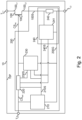
- power switch assembly 10 includes power switch 100 and overcurrent handling logic 200.
- Power switch assembly 10 has an assembly control terminal T C , a first assembly load terminal T L1 and a second assembly load terminal T L2 .
- Assembly control terminal T C , first assembly load terminal T L1 and second assembly load terminal T L2 may be comprised in a package 10P.
- Package 10P may thus enclose power switch 100 and overcurrent logic 200.
- Power switch 100 has a control terminal 100 C , a first load terminal 100 L1 and a second load terminal 100 L2 . These terminals are respectively coupled to assembly control terminal T C , first assembly load terminal T L1 and second assembly load terminal T L2 .
- the expression “coupled” refers to both direct connections and connections with intervening elements, the latter being the case for control terminal 100 C , first load terminal 100 L1 and second load terminal 100 L2 and assembly control terminal T C , first assembly load terminal T L1 and second assembly load terminal T L2 , respectively.
- Power switch 100 may be any kind of power switch configured to have a high voltage blocking capability.
- power switch 100 may be able to block voltages above at least 400V, such as 450V, 900V, 1200V or 1800V.
- power switch 10 may for example be a silicon or silicon carbide (SiC) metal oxide field effect transistor (MOSFET), a silicon or SiC insulated gate bipolar transistor (IGBT) or a Gallium nitride high electron mobility transistor (GaN-HEMT). It will be understood that both the voltage levels and the technology types discussed with regard to power switch 10 are merely provided as an example. The present disclosure may be practiced with other high voltage levels and other power switch technologies than those mentioned here.
- SiC silicon or silicon carbide
- MOSFET metal oxide field effect transistor
- IGBT silicon or SiC insulated gate bipolar transistor
- GaN-HEMT Gallium nitride high electron mobility transistor
- Power switch 100 may, in some implementations of the present disclosure, include current sense capability. That is, power switch 100 may be configured to provide a signal indicative of a load current I L of power switch 100, i.e. the current flowing between first load terminal 100 L1 and second load terminal 100 L2 , to overcurrent handling logic 200, for example.
- the current sense capability may for example be implemented by branching off a current flowing through some of the transistor cells forming power switch 100, such as 1 or 10 transistor cells. It will be understood that the current sense capability may also be provided in other ways and that in some examples of the present disclosure the current sense capability may not be present.
- load current may be directly used to detect an overcurrent condition.
- Overcurrent handling logic 200 is coupled between assembly control terminal T C and control terminal 100 C as well as between second load terminal 100 L2 and second assembly load terminal T L2 .
- assembly control terminal T C may be coupled to an external control signal line CS ext
- control terminal 100 C may be coupled to an internal control signal line CS int
- second load terminal 100 L2 may be coupled to a load current signal line 100S
- second assembly load terminal T L2 may be coupled to a ground signal line 200G.
- overcurrent detection circuit 200 is configured to detect an overcurrent condition of load current I L and to handle, i.e. to control, a voltage V CL2 between control terminal 100 C and second load terminal 100 L2 .
- overcurrent handling logic 200 can further be configured to detect the overcurrent condition in a temperature-compensated manner and further controls voltage V CL2 and thereby load current IL in a way which avoids voltage surges at power switch 100 at parasitic inductances, such as parasitic inductance L par.
- Overcurrent handling logic 200 includes an overcurrent detection circuit 240 and a discharge current generation circuit 230. Overcurrent handling logic 200 may further comprise a power supply generation circuit 210 and a control path control circuit 220. The various circuits of overcurrent handling logic 200 will be discussed in the following.
- Power supply generation circuit 210 may be configured to generate a power supply for at least one of overcurrent detection circuit 240, discharge current generation circuit 230 and control path control circuit 220 based on a voltage supplied by a gate driver, such as gate drivers 20H and 20L of Fig. 1 , coupled to assembly control terminal T C and second assembly load terminal T L2 .
- a gate driver such as gate drivers 20H and 20L of Fig. 1
- power supply generation circuit 210 may be coupled between external control signal line CS ext and ground signal line 200G.
- power supply generation circuit 210 uses a voltage difference between external control signal line CS ext and ground signal line 200G generated by an external gate driver to provide a power supply to components of overcurrent handling logic 200.
- Power supply generation circuit 210 may provide the generated power supply to the components of overcurrent handling logic 200 via power supply line 210S.
- Basing the generation of the power supply voltage of overcurrent handling logic 200 on the above-discussed voltage difference may ensure that power switch assembly 10 appears as a regular power switch when looking at the pin-out of power switch assembly 10, i.e. power switch assembly 10 has a pin-out like a power switch without any logic co-packaged with it. Further, such an arrangement may ensure that the internal control provided by overcurrent handling logic 200 cannot turn on power switch 100 if a gate driver controlling power switch assembly 10 provides a turn-off signal to power switch assembly 10.
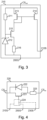
- power supply generation circuit 210 may include a resistor 211, a Zener diode 212, three transistors 213 to 215 and a resistor 216. Resistor 211, Zener diode 212, transistor 215 and resistor 216 are configured to generate a current based on the voltage difference between signal line CS ext and 200G. This current is then mirrored to power supply line 210S by a current mirror formed by transistors 213 and 214.
- the current mirror formed by transistors 213 and 214 may be used to amplify the current resistor 211, Zener diode 212, transistor 215 and resistor 216 if a gain of the current mirror formed by transistors 213 and 214 is larger than 1. This may for example be achieved by designing transistors 213 and 214 with different transistor parameters or by implementing transistors 213 and 214 as multiple transistors with identical transistor parameters respectively in parallel but with different numbers of parallel transistors.
- overcurrent handling logic 200 the functionality of power supply generation circuit 210 may be integrated into at least one of overcurrent detection circuit 240, discharge current generation circuit 230 and control path control circuit 220. That is, in such exemplary implementations, overcurrent handling logic 200 may not include power supply generation circuit 210. Instead, overcurrent detection circuit 240, discharge current generation circuit 230 and control path control circuit 220 may in such exemplary implementations implement their individual power supplies based on the voltage difference between control signal line CS ext and ground signal line 200G.
- overcurrent detection circuit 240, discharge current generation circuit 230 and control path control circuit 220 may not require a power supply and may be operated based on the detection of an overcurrent condition of load current I L .
- an overcurrent detection signal 240S which will be discussed later, may provide the power to operate overcurrent detection circuit 240, discharge current generation circuit 230 and control path control circuit 220.
- both approaches i.e. providing operating power to the components of overcurrent handling logic 200 based on the voltage difference between control signal line CS ext and ground signal line 200G and based on the load current I L may be mixed. That is, in some exemplary embodiments, some components of overcurrent handling logic 200 may be supplied by one of power supply generation circuit 210 or internal power supply and some components may be supplied by overcurrent detection signal 240S.
- Control path control circuit 220 may be coupled between assembly control terminal T C and control terminal 100 C and may be configured to switchably couple assembly control terminal T C to control terminal 100 C .
- switchably coupling may refer to the fact that control path control circuit 220 may be configured to switch between a variety of coupling states, which may for example include a decoupling state and a coupling state. In the decoupling state, control path control circuit 220 may provide a high impedance between assembly control terminal T C and control terminal 100 C while at the same time enabling sinking of a current from control terminal 100 C to assembly control terminal T C .
- control path control circuit 220 may provide a low impedance between assembly control terminal T C and control terminal 100 C , thereby enabling control of the control terminal 100 C via external control signal line CS ext .
- control path control circuit 220 may switchably couple external control signal line CS ext to internal control signal line CS in .
- Control path control circuit 220 may thereby enable overcurrent handling logic 200 to switch between external control via an external gate driver and internal control via overcurrent handling logic 200 following the detection of an overcurrent condition. Therefore, control path control circuit 220 may in some implementations be configured to decouple assembly control terminal T C from control terminal 100 C responsive to overcurrent detection signal 240S.
- Control path control circuit 220 may further be configured to keep assembly control terminal T C and thus external control signal line CS ext decoupled from control terminal 100 C (and thus internal control signal line CS int ) until a voltage supplied by an external gate driver coupled to assembly control terminal T C and second assembly load terminal T L2 falls below a threshold voltage of power switch 100 and/or until another predefined condition is met, such as when the detected overcurrent condition has passed. That is, control path control circuit 220 may keep power switch assembly 10 in an internal control state until an external gate driver stops to supply a turn-on signal to power switch assembly 10.
- control path control circuit 220 may include a control path switch 221, a diode 222, a resistor 223 and a gate driver 224.
- Control path switch 221 may, based on one of a signal from gate driver 224, control path modulation signal 230S or overcurrent detection signal 240S, switchably couple external control signal line CS ext to internal control signal line CS int .
- Gate driver 224 may be a gate driver similar to gate drivers 20H and 20L and may be configured to couple control path switch 221 to a voltage level causing control path switch 221 to be in a conductive state and to a voltage level causing control path switch 221 to be in a blocking state based on overcurrent detection signal 240S. These voltage level may for example correspond to power supply line 210S and to ground signal line 200G or may be derived by gate driver 224 from power supply line 210S and from ground signal line 200G (connection to ground signal line 200G not shown in Figs. 2 and 4 for simplicity).
- control path switch 221 may be directly coupled to overcurrent detection signal 240S in a manner ensuring that control path switch 221 decouples external control signal line CS ext from internal control signal line CS int if overcurrent detection signal 240S indicates an overcurrent condition.
- control path switch 221 may for example be a normally-on device or overcurrent detection signal 240S may be invertedly provided to control path switch 221.
- control path switch 221 may receive control path modulation signal 230S determined by overcurrent detection circuit 240, which will be discussed below. Accordingly, in some implementations of the present disclosure, control path control circuit 220 may be controlled by overcurrent detection circuit 240.
- Resistor 223 may, if control path switch 221 couples external control signal line CS ext to internal control signal line CS int , provide a current to control terminal 100 C based on the voltage applied by an external gate driver at assembly control terminal T C .
- Diode 222 is coupled in parallel with control path switch 221.
- the cathode of diode 222 is coupled to external control signal line CS ext and the anode of diode 222 is coupled to internal control signal line CS int .
- diode 222 is reverse biased while an external gate driver applies a voltage to assembly control terminal T C exceeding the voltage level of internal control signal line CS int .
- diode 222 may become forward biased and thus conductive if an external gate driver pulls a voltage applied at assembly control terminal T C below the voltage level of internal control signal line CS int .
- diode 222 may provide a path to sink current from control terminal 100 C if an external gate driver indicates that power switch assembly should be turned into a blocking state. This may expedite switching power switch 100 to the blocking state.
- Diode 222 may be a body diode of control path switch 221 or may be a freewheeling diode provided with control path switch 221. It will be understood that diode 222 may be omitted in implementations of the present disclosure which do not require the current sinking functionality provided by diode 222.
- Discharge current generation circuit 230 is coupled to overcurrent detection circuit 240, control terminal 100 C and second load terminal 100 L2 via ground signal line 200G. Based on this arrangement, discharge current generation circuit 230 is configured to generate a discharge current I dis to at least partially discharge control terminal 100 C responsive to overcurrent detection signal 240S. In other words, discharge current generation circuit 230 at least partially discharges control terminal 100. For example, discharge current generation circuit 230 may at least partially discharge a capacitance of power switch 100 at control terminal 100, by providing the discharge current I dis , which flows from control terminal 100 C to second load terminal 100 L2 .
- the discharge current I dis may be based on a fall time t fall , wherein fall time t fall defines a timeframe from the detection of the overcurrent condition of load current I L to a reduction of the load current I L to a safety current value I safe .
- Safety current value I safe may for example correspond to a safety voltage level V safe of voltage V CL2 . That is, timeframe t fall approximately determines a rate of change over time of load current I L . While this changing of load current I L may lead to a voltage surge due to parasitic inductance L par , timeframe t fall is determined such that such voltage surge is acceptable in light of a maximum blocking voltage of power switch 100.
- fall time t fall is determined based on a difference between the load current I L and safety current value I safe and based on the parasitic inductance L par and maximum blocking voltage of the power switch 100, such that a voltage across the first load terminal 100 L1 and second load terminal 100 L2 of the power switch 100, including a voltage surge caused by a change of the load current I L , does not exceed the maximum blocking voltage of the power switch 100.
- the upper signaling diagram of Fig. 6 illustrates load current I L and a voltage V L1L2 between first load terminal 100 L1 and second load terminal 100 L2 over time with regard to signal value levels I safe , I over , V DC+ and V over .
- load current I L increases to overcurrent detection level I over , at which point overcurrent detection circuit 240 detects the overcurrent condition of load current I L .
- overcurrent detection circuit 240 provides overcurrent detection signal 240S.
- discharge current generation circuit 230 provides the discharge current I dis , which causes load current I L to be reduced from overcurrent current level I over to safety current level I safe during fall time t fall .
- the reduction of load current I L from overcurrent current level I over to safety current level I safe may be referred to as ⁇ I L .
- voltage V L1L2 increases above V DC+ , i.e. the high voltage supply coupled to power switch assembly 10, to overcurrent voltage level V over .
- This increase is due to a voltage surge induced by parasitic inductance L par , which is a result of overcurrent handling logic 200 discharging control terminal 100 C after detecting the overcurrent condition. Since parasitic inductance L par is coupled in series with power switch 10, as shown in Fig.
- Safety load current value I safe may be a current value above 0 A but below a rated nominal current I nom of power switch 100 and may be selected based on the specific application in which the power switch assembly is to be employed. In other words, the discharge current I dis discharges the control terminal 100 C , for example a capacitance at control terminal 100 C , to a charge level corresponding to safety load current value I safe . Since safety load current value I safe may be a current value above 0 A, as shown in the upper signaling diagram of Fig.
- the discharge current may not fully discharge control terminal 100 C , for example the discharge current I dis may only partially discharge control terminal 100 C .
- safety load current value I safe may in some implementations be 0 A, in which case the discharge current I dis fully discharges control terminal 100 C .
- the lower signaling diagram of Fig. 6 illustrates a voltage V CL2 over time, i.e. the voltage between control terminal 100 C and 100 L2 .
- V CL2 the voltage between control terminal 100 C and 100 L2 .
- the discharge current I dis can thus be determined independent of the area of power switch 100.
- a current value of the discharge current I dis can be determined, which quickly discharges control terminal 100 C while avoiding voltage levels of overcurrent voltage V over which exceed the breakdown voltage of power switch 100.
- the value I dis determined using equation (8) represents a maximum value for a given parasitic inductance L par value to achieve fastest discharge of control terminal 100 C under the noted boundary conditions, and a lower value of I dis may be used to account for variations of the parameters entering into equation (8) to provide for a safety margin, for example.
- Discharge current I dis may for example be an essentially constant current having, as an upper limit, a value that is determined based on equation (8) above.
- Essentially constant is to be construed, in this case, as a current that does not drop more than up to a maximum predetermined fraction, for example up to 10%, up to 20%, up to 30%, up to 40%, or up to 50%, below a nominal value of discharge current I dis , excluding switching on or switching off transitions of the discharge current.
- discharge current I dis can be an essentially constant current having a value that is lower than the maximum value, for example a current value below the maximum value according to safety margin, such as 5% or 10% or 20% or up to 50% lower than the maximum value.
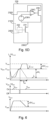
- Discharge current generation circuit 230 may be implemented in accordance with the above discussion as shown in Figs. 5A to 5D .
- the discharge current generation circuit 230 of Figs. 5A to 5D may include a discharge switch 231, which causes discharge current generation circuit 230 to discharge control terminal 100 C with the discharge current.
- Discharge switch 231 may be controlled by one of a gate driver 232 or directly by overcurrent detection signal 240S.
- Gate driver 232 may be similar to gate driver 224 of control path control circuit 220, i.e. it may couple discharge switch 231 to a supply voltage corresponding to a conducting state of discharge switch 231 and to a supply voltage corresponding to a blocking state of discharge switch 231.
- discharge current generation circuit 230 may in addition comprise a current source 233 and a voltage source 234.
- Current source 233 may provide the above-discussed discharge current.
- Voltage source 234 may provide voltage V safe discussed above. Since discharge current generation circuit 230 is coupled between control terminal 100 C and second load terminal 100 L2 when discharge switch 231 is in the conducting state, voltage source 234 may cause voltage V CL2 to be reduced to voltage V safe .
- Voltage source 234 may for example be implemented by a Zener diode 234, as shown in Fig. 5B .
- Current source 233 may be implemented as shown in Fig. 5C , that is with a current source switch 235, a diode 236, a Zener diode 238 and a biasing current source 237.
- switch 221 may be in a conducting state while switch 231 is in a blocking state and vice versa, as indicated by voltages V 221 and V 231 in the middle signal diagram of Fig. 6 .
- a control of switches 221 and 231 may be achieved based on overcurrent detection signal 240S.
- such a control of switches 221 and 231 may be achieved based on control path modulation signal 230S, which may be provided by discharge current generation circuit 230 of Fig. 5D .
- Discharge current generation circuit 230 of Fig. 5D may include voltage source 239V, a voltage comparator 239C and modulation switch 239. Modulation signal 230S is thus based on the voltage at a first load terminal of modulation switch 239. Modulation switch 239 is controlled by the result of the comparison of voltage comparator 239C with the voltage level of control path modulation signal 230S. Control path modulation signal 230S causes the impedance of switch 221 to vary to thereby vary voltage V CL2 , for example to reduce voltage V CL2 to voltage level V safe . In other words, control path modulation signal 230S may be used by overcurrent handling logic 200 to perform internal control of power switch 100 by modulating external control signal CS ext based on the impedance of switch 221.
- Overcurrent detection circuit 240 is coupled between second load terminal 100 L2 and second assembly load terminal T L2 and provides overcurrent detection signal 240S. As will be discussed in the following, overcurrent detection circuit 240 is configured to detect an overcurrent condition of load current I L and to compensate a temperature coefficient of overcurrent detection circuit 240 in order to prevent erroneous detections of overcurrent conditions. Overcurrent detection signal 240S may thus also be referred to as temperature-compensated overcurrent detection signal 240S.
- overcurrent detection circuit 240 needs to detect an overcurrent condition of load current I L in a short time frame, such as 100 ns.
- overcurrent detection circuit 240 is configured to maintain at least a part of overcurrent detection circuit 240 in a linear operating region during operation of power switch assembly 10.
- Power switch assembly 10 is in operation while an external gate driver applies a voltage across assembly control terminal T C and second assembly load terminal T L2 .
- the linear operating region refers to an operating region of a semiconductor device, such as a MOSFET or a bipolar junction transistor (BJT), in which the semiconductor device behaves like a voltage-controlled current source.
- a change of the gate voltage of the semiconductor device causes a proportional and essentially instant change of the current through the semiconductor device.
- a signal such as a signal indicative of load current I L .
- overcurrent detection circuit 240 With overcurrent detection circuit 240 maintaining at least a part of overcurrent detection circuit 240 in the linear operating mode, overcurrent detection circuit 240 is further configured to detect an overcurrent condition of load current I L in a manner complying with the detection speed requirement discussed above. This enables overcurrent detection circuit 240 to compensate a temperature coefficient of the overcurrent detection circuit to provide temperature-compensated overcurrent detection signal 240S while complying with the detection speed requirement. In other words, maintaining at least a part of overcurrent detection circuit 240 in the linear operating mode, enables overcurrent detection circuit 240 to compensate the temperature coefficient without delaying the detection of the overcurrent condition.
- overcurrent detection circuit 240 may comprise a current measurement resistor 242 resistor coupled between second load terminal 100 L2 and second assembly load terminal T L2 .
- Current measurement resistor 242 may have a current measurement temperature coefficient.
- current measurement resistor 242 may be a copper shunt with a temperature coefficient of 3.9*10 -3 1/°C.
- overcurrent detection circuit 240 may comprise a temperature compensation circuit 241, which is coupled to current measurement resistor 241.
- Temperature compensation circuit 241 may have a compensation temperature coefficient. The compensation temperature coefficient may be chosen to compensate the current measurement temperature coefficient.
- the compensation temperature coefficient may be of the same value but have a different sign than the current measurement temperature coefficient or may be of the same sign but arranged in a manner to counteract the current measurement temperature coefficient.
- overcurrent detection circuit 240 including temperature compensation circuit 241 and current measurement resistor 242, it is at least a part of temperature compensation circuit 241 which may be maintained in the linear operating region during operation of the power switch assembly.
- temperature compensation circuit 241 may comprise a temperature coefficient compensation circuit 241T, a linear region maintenance and conversion circuit 241L and an overcurrent signal output stage 2410.
- Temperature coefficient compensation circuit 241T may be coupled to current measurement resistor 242 and to linear region maintenance and conversion circuit 241L and may have the compensation temperature coefficient.
- Linear region maintenance and conversion circuit 241L may be coupled to temperature coefficient compensation circuit 241T and to overcurrent signal output stage 2410.
- Linear region maintenance and conversion circuit 241L may be configured to maintain at least a part of temperature coefficient compensation circuit 241 T in the linear operating region. Further, linear region maintenance and conversion circuit 241L may also be configured to increase a dynamic range of temperature-compensated overcurrent detection signal 240S.
- Overcurrent signal output stage 2410 may be coupled to linear region maintenance and conversion circuit 241L and may be configured to provide temperature-compensated overcurrent detection signal 240S based on a comparison of an output of linear region maintenance and conversion circuit 241L with an overcurrent threshold value.
- the overcurrent threshold value may for example be inherently generated by temperature coefficient compensation circuit 241T.
- overcurrent signal output stage 2410 may also be coupled to temperature coefficient compensation circuit 241T.
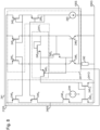
- Fig. 8 illustrates a detailed exemplary implementation of temperature compensation circuit 241 and thereby of temperature coefficient compensation circuit 241T, linear region maintenance and conversion circuit 241L and overcurrent signal output stage 2410, which are respectively indicated within Fig. 8 by dashed boxes.
- temperature coefficient compensation circuit 241T may include switches 245 1 to 245 5 , bipolar transistors 246 1 and 246 2 and a biasing current source 243.
- Bipolar transistors 246 1 and 246 2 may also be referred to as compensation transistors.
- Bipolar transistors 246 1 and 246 2 may be arranged to cause a voltage drop exhibiting the compensation temperature coefficient at current measurement resistor 242 caused by temperature coefficients of bipolar transistors 246 1 and 246 2 . This voltage drop may cancel out the current measurement temperature coefficient of resistor 242. Based on the voltage drop, the signal indicative of load current IL may thus be temperature-compensated, which may lead to overcurrent detection signal 240S being temperature-compensated.
- Linear region maintenance and conversion circuit 241L may comprise switches 245 6 and 245 7 .
- Switch 245 6 is arranged with regard to bipolar transistor 256 1 to maintain bipolar transistor 256 1 in the linear operating region.
- the temperature-compensated signal indicative of load current I L is initially provided as a voltage signal at the signal line between bipolar transistors 246 1 and 246 2 .
- Switch 245 7 may be arranged to convert this voltage signal to a current signal indicative of load current I L . Together with the conversion, switch 245 7 may increase the dynamic range of the temperature-compensated signal indicative of load current I L .
- Overcurrent signal output stage 2410 may comprise switches 245 8 to 245 12 and a biasing voltage source 244. Switches 245 11 and 245 12 may form a current mirror mirroring the current signal indicative of load current I L .
- Transistors 245 8 and 245 9 may be coupled to temperature coefficient compensation circuit 241T to receive the overcurrent threshold value and accordingly couple the output of overcurrent signal output stage 2410 to power supply line 210S if the current signal indicative of load current I L is indicative of an overcurrent condition of load current I L .
- Fig. 9 provides a flowchart of a method 300 for operating overcurrent handling logic 200. Optional steps of method 300 are illustrated as dashed boxes in Fig. 9 .
- step 310 method 300 may maintain at least a part of overcurrent detection logic 200 in the linear operating region during operation of power switch assembly 10.
- step 320 method 300 detects an overcurrent condition at second load terminal 100 L2 to provide overcurrent detection signal 240S.
- step 330 method 300 may compensate the temperature coefficient of overcurrent detection circuit 240 to provide temperature-compensated overcurrent detection signal 240S.
- step 340 method 300 generates the discharge current.
- step 350 method 300 at least partially discharges control terminal 100 C responsive to temperature-compensated overcurrent detection signal 240S with the discharge current.
- power switch assembly 10 may only include the temperature-compensated overcurrent detection and use other means of internally controlling power switch 100 upon detection of an overcurrent condition.
- power switch assembly 10 may only include the discharge current generation discussed herein and may rely on other means of internal overcurrent detection.
- the invention may further be illustrated by the following examples.
- a power switch assembly having an assembly control terminal, a first assembly load terminal and a second assembly load terminal, may comprise a power switch having a control terminal coupled to the assembly control terminal, a first load terminal coupled to the first assembly load terminal and a second load terminal coupled to the second assembly load terminal, and an overcurrent handling logic coupled between the assembly control terminal and the control terminal and between the second load terminal and the second assembly load terminal, including an overcurrent detection circuit coupled between the second load terminal and the second assembly load terminal and configured to provide an overcurrent detection signal indicative of an overcurrent condition of a load current of the power switch, and a discharge current generation circuit coupled to the overcurrent detection circuit and the control terminal and configured to generate a discharge current to at least partially discharge the control terminal responsive to the overcurrent detection signal.
- the power switch assembly may further comprise a package configured to enclose the overcurrent handling logic and the power switch, wherein the package comprises the assembly control terminal, the first assembly load terminal and the second assembly load terminal.
- the package exclusively comprises the assembly control terminal, the first assembly load terminal and the second assembly load terminal and no other or further terminals.
- the discharge current may be based on a fall time, wherein the fall time defines a timeframe from the detection of the overcurrent to a reduction of the load current to a safety load current value.
- the overcurrent handling logic may further comprise a control path control circuit coupled between the assembly control terminal and the control terminal, and the control path control circuit may further be configured to switchably couple the assembly control terminal to the control terminal.
- control path control circuit may be configured to decouple the assembly control terminal from the control terminal responsive to the overcurrent detection signal.
- control path control circuit may further be configured to keep the assembly control terminal decoupled from the control terminal until a voltage supplied by a gate driver coupled to the assembly control terminal and the second assembly load terminal falls below a threshold voltage of the power switch.
- the discharge current generation circuit may be configured to generate the discharge current such that the control terminal is discharged until the load current reaches or falls below a safety load current value.
- the overcurrent detection circuit may be configured to compensate a temperature coefficient of the overcurrent detection circuit to provide a temperature-compensated overcurrent detection signal.
- the overcurrent detection circuit may comprise a current measurement resistor coupled between the second load terminal and the second assembly load terminal having a current measurement temperature coefficient, and a temperature compensation circuit coupled to the current measurement resistor having a compensation temperature coefficient, wherein the compensation temperature coefficient may compensate the current measurement temperature coefficient.
- the overcurrent detection circuit may be configured to maintain at least a part of the overcurrent detection circuit in a linear operating region during operation of the power switch assembly.
- At least a part of the temperature compensation circuit may be maintained in the linear operating region during operation of the power switch assembly.
- the temperature compensation circuit may comprise a temperature coefficient compensation circuit having the compensation temperature coefficient; and a linear region maintenance and conversion circuit coupled to the temperature coefficient compensation circuit and configured to maintain at least a part of the temperature coefficient compensation circuit in the linear operating region.
- the temperature compensation circuit may further comprise an overcurrent signal output stage coupled to the linear region maintenance and conversion circuit and configured to provide the temperature-compensated overcurrent detection signal based on a comparison of an output of the linear region maintenance and conversion circuit with an overcurrent threshold value.
- the temperature coefficient compensation circuit may include at least one compensation transistor having the compensation temperature coefficient, and the at least one compensation switch may be maintained in the linear operating region.
- the linear region maintenance and conversion circuit may further be configured to increase a dynamic range of the temperature-compensated overcurrent detection signal.
- the overcurrent handling logic may further comprise a power supply generation circuit configured to generate a power supply for at least one of the overcurrent detection circuit, the discharge current generation circuit and the control path control circuit based on a voltage supplied by a gate driver coupled to the assembly control terminal and the second assembly load terminal.
- a method for operating an overcurrent handling logic of a power switch assembly comprising detecting an overcurrent condition at a second load terminal of a load current of the power switch to provide an overcurrent detection signal indicative of the overcurrent condition of the load current of the power switch, and generating a discharge current, and at least partially discharging a control terminal of the power switch responsive to the overcurrent detection signal with the discharge current.
- the method may further comprise maintaining at least a part of the overcurrent detection logic in a linear operating region during operation of the power switch assembly.
- the method may further comprise compensating a temperature coefficient of the overcurrent detection circuit to provide a temperature-compensated overcurrent detection signal.
- a power switch assembly having an assembly control terminal, a first assembly load terminal and a second assembly load terminal, may comprise a power switch having a control terminal coupled to the assembly control terminal, a first load terminal coupled to the first assembly load terminal and a second load terminal coupled to the second assembly load terminal, and an overcurrent handling logic coupled between the assembly control terminal and the control terminal and between the second load terminal and the second assembly load terminal, including an overcurrent detection circuit coupled between the second load terminal and the second assembly load terminal and configured to detect an overcurrent condition of a load current of the power switch, and compensate a temperature coefficient of the overcurrent detection circuit to provide a temperature-compensated overcurrent detection signal, wherein the compensation of the temperature coefficient does not delay the detection of the overcurrent condition, and a discharge current generation circuit coupled to the overcurrent detection circuit and the control terminal and configured to generate a discharge current to discharge the control terminal responsive to the temperature-compensated overcurrent detection signal.
- a power switch assembly having an assembly control terminal, a first assembly load terminal and a second assembly load terminal, may comprise a power switch having a control terminal coupled to the assembly control terminal, a first load terminal coupled to the first assembly load terminal and a second load terminal coupled to the second assembly load terminal, and an overcurrent handling logic coupled between the assembly control terminal and the control terminal and between the second load terminal and the second assembly load terminal, including an overcurrent detection circuit coupled between the second load terminal and the second assembly load terminal and configured to maintain at least a part of the overcurrent detection circuit in a linear operating region during operation of the power switch assembly, detect an overcurrent condition of a load current of the power switch, and compensate a temperature coefficient of the overcurrent detection circuit to provide a temperature-compensated overcurrent detection signal, and a control terminal control circuit coupled to the overcurrent detection circuit and the control terminal and configured to control the control terminal responsive to the temperature-compensated overcurrent detection signal.
- a power switch assembly having an assembly control terminal, a first assembly load terminal and a second assembly load terminal, comprises a power switch having a control terminal coupled to the assembly control terminal, a first load terminal coupled to the first assembly load terminal and a second load terminal coupled to the second assembly load terminal, and an overcurrent handling logic coupled between the assembly control terminal and the control terminal and between the second load terminal and the second assembly load terminal, including an overcurrent detection circuit coupled between the second load terminal and the second assembly load terminal and configured to maintain at least a part of the overcurrent detection circuit in a linear operating region during operation of the power switch assembly, detect an overcurrent condition of a load current of the power switch, and compensate a temperature coefficient of the overcurrent detection circuit to provide a temperature-compensated overcurrent detection signal, and a discharge current generation circuit coupled to the overcurrent detection circuit, the control terminal and the second load terminal and configured to generate a discharge current to at least partially discharge the control terminal responsive to the temperature-compensated overcurrent detection signal.
Landscapes
- Physics & Mathematics (AREA)
- General Physics & Mathematics (AREA)
- Engineering & Computer Science (AREA)
- Power Engineering (AREA)
- Emergency Protection Circuit Devices (AREA)
- Electronic Switches (AREA)
- Power Conversion In General (AREA)
Abstract
Description
- The invention generally relates to overcurrent protection of power switches and more precisely to overcurrent protection provided inside a power switch assembly.
- During operation, a power switch may encounter abnormally high load path currents, i.e. overcurrent or short circuit conditions, which can damage the power switch. To avoid damage to the power switch, various solutions external to and co-packaged with the power switch exist, which detect an overcurrent and turn off the power switch. Given the switching speed of modern power switches, the timeframe to detect an overcurrent can be very short so that high-speed detection logic must be used.
- In addition, present overcurrent detection handling solutions do not consider parasitic inductances in series with the load path of the power switch. Depending on the speed and the level to which the load current is reduced following detection of an overcurrent, such parasitic inductances may cause voltage surges at the power switch, which may inadvertently damage the power switch.
- Therefore, it is an objective of the present invention to improve the protection of power switches with regard to overcurrent or short-circuit conditions.
- To achieve this objective, the present invention provides a power switch assembly having an assembly control terminal, a first assembly load terminal and a second assembly load terminal, comprising a power switch having a control terminal coupled to the assembly control terminal, a first load terminal coupled to the first assembly load terminal and a second load terminal coupled to the second assembly load terminal and an overcurrent handling logic coupled between the assembly control terminal and the control terminal and between the second load terminal and the second assembly load terminal, including an overcurrent detection circuit coupled between the second load terminal and the second assembly load terminal and configured to detect an overcurrent of a load current of the power switch, and a discharge current generation circuit coupled to the overcurrent detection circuit, the control terminal and the second load terminal and configured to generate a discharge current to at least partially discharge the control terminal responsive to the temperature-compensated overcurrent detection signal.
- The present invention further provides a method for operating an overcurrent handling logic of a power switch assembly, the overcurrent handling logic comprising an overcurrent detection logic and a discharge current generation circuit, the method comprising detecting an overcurrent at a load a second load terminal of a power switch of the power switch assembly, generating a discharge current and at least partially discharging a control terminal of the power switch responsive to the overcurrent detection signal with the discharge current.
- Embodiments of the present invention will be described with reference to the following appended drawings, in which like reference signs refer to like elements.
-
FIG. 1 illustrates a half-bridge topology including power switch assemblies according to embodiments of the present invention. -
FIG. 2 provides a block diagram of the power switch assembly according to embodiments of the present invention. -
FIG. 3 illustrates an exemplary power supply of the overcurrent handling logic according to embodiments of the present invention. -
FIG. 4 illustrates an exemplary control path control circuit of the power switch assembly according to embodiments of the present invention. -
FIGS. 5A to 5D illustrate exemplary implementations of the discharge current generation circuit of the power switch assembly according to embodiments of the present invention. -
FIG. 6 illustrates various signals illustrating the operation of the discharge current generation circuit of the power switch assembly according to embodiments of the present invention. -
FIG. 7 provides a block diagram of the temperature compensation circuit of the power switch assembly according to embodiments of the present invention. -
FIG. 8 illustrates an exemplary implementation of the temperature compensation circuit of the power switch assembly according to embodiments of the present invention. -
Fig. 9 provides a flowchart of a method for operating an overcurrent handling logic of the power switch assembly according to embodiments of the present invention. - It should be understood that the above-identified drawings are in no way meant to limit the disclosure of the present invention. Rather, these drawings are provided to assist in understanding the invention. The person skilled in the art will readily understand that aspects of the present invention shown in one drawing may be combined with aspects in another drawing or may be omitted without departing from the scope of the present invention.
- The present disclosure generally provides a power switch assembly which includes a power switch and an overcurrent handling logic. The overcurrent handling logic is configured to detect an overcurrent through a load path of the power switch and to generate a discharge current. The discharge current at least partially discharges, in response to the overcurrent detection, a control terminal of the power switch. The discharge current is configured to quickly cause a reduction of the load current to a safe value while not discharging the control terminal too quickly to cause a voltage surge at parasitic inductances coupled in series with the power switch. Further, to avoid erroneous overcurrent detections, an overcurrent detection circuit of the overcurrent handling logic may be temperature-compensated, i.e. the overcurrent detection may be configured to compensate a temperature coefficient of at least a part of the overcurrent detection circuit. Since the temperature compensation is not to impact the detection speed, at least a part of the overcurrent detection may be maintained in a linear operating region. This enables fast detection of an overcurrent while at the same time enabling compensation of a temperature coefficient of at least a part of the overcurrent detection circuit.
- This general concept will be explained with reference to the appended drawings with
Fig. 1 illustrating a typical application of the power switch assembly andFig. 2 providing a block diagram of the power switch assembly. Based on the block diagram ofFig. 2 , various exemplary implementation details of the blocks of the power switch assembly will be described in detail with regard toFigs. 3 to 8 , moving from left to right throughFig. 2 . Finally,Fig. 9 will provide a flow chart of the method performed by the overcurrent handling logic of the power switch assembly. -
FIG. 1 schematically illustrates a half-bridge topology formed bypower switch assemblies power switch assembly 10H is coupled between a supply voltage DC+ and an output of the half-bridge, while low sidepower switch assembly 10L is coupled between the output of the half bridge and a supply voltage DC-. The half-bridge further includes parasitic inductances in series withpower switch assemblies side switch assembly 10H and the output of the half-bridge. It will be understood that parasitic inductances may be also present between the output of the half-bridge and the low side switching assembly or between the respective switching assemblies and the supply voltages DC+ and DC-. Lpar may thus also be considered as the equivalent inductance of all parasitic inductances of the half-bridge. -
Power switch assemblies gate drivers Gate drivers gate drivers gate drivers power switch 10. In a further example,gate drivers gate drivers gate drivers gate drivers gate drivers power switch assemblies - Finally, each one of the power switch assemblies 10H and 10L includes a
power switch 100 and anovercurrent handling logic 200, which will be discussed in detail with regard toFig. 2 . We note that theswitches 100 of the power switch assemblies 10H and 10L may be the same or may be different to each other. -
Fig. 2 provides a block diagram of apower switch assembly 10, which is an example of thepower switch assemblies Fig. 1 . Thus,power switch assembly 10 includespower switch 100 andovercurrent handling logic 200. -
Power switch assembly 10 has an assembly control terminal TC, a first assembly load terminal TL1 and a second assembly load terminal TL2. Assembly control terminal TC, first assembly load terminal TL1 and second assembly load terminal TL2 may be comprised in a package 10P. Package 10P may thus enclosepower switch 100 andovercurrent logic 200. -
Power switch 100 has acontrol terminal 100C, afirst load terminal 100L1 and asecond load terminal 100L2. These terminals are respectively coupled to assembly control terminal TC, first assembly load terminal TL1 and second assembly load terminal TL2. As can be seen inFig. 2 and as will be understood throughout this disclosure, the expression "coupled" refers to both direct connections and connections with intervening elements, the latter being the case forcontrol terminal 100C,first load terminal 100L1 andsecond load terminal 100L2 and assembly control terminal TC, first assembly load terminal TL1 and second assembly load terminal TL2, respectively. -
Power switch 100 may be any kind of power switch configured to have a high voltage blocking capability. For example,power switch 100 may be able to block voltages above at least 400V, such as 450V, 900V, 1200V or 1800V. To achieve such voltage blocking capabilities,power switch 10 may for example be a silicon or silicon carbide (SiC) metal oxide field effect transistor (MOSFET), a silicon or SiC insulated gate bipolar transistor (IGBT) or a Gallium nitride high electron mobility transistor (GaN-HEMT). It will be understood that both the voltage levels and the technology types discussed with regard topower switch 10 are merely provided as an example. The present disclosure may be practiced with other high voltage levels and other power switch technologies than those mentioned here. -
Power switch 100 may, in some implementations of the present disclosure, include current sense capability. That is,power switch 100 may be configured to provide a signal indicative of a load current IL ofpower switch 100, i.e. the current flowing betweenfirst load terminal 100L1 andsecond load terminal 100L2, to overcurrent handlinglogic 200, for example. The current sense capability may for example be implemented by branching off a current flowing through some of the transistor cells formingpower switch 100, such as 1 or 10 transistor cells. It will be understood that the current sense capability may also be provided in other ways and that in some examples of the present disclosure the current sense capability may not be present. For example, in some examples of the present disclosure, load current may be directly used to detect an overcurrent condition. -
Overcurrent handling logic 200 is coupled between assembly control terminal TC and control terminal 100C as well as betweensecond load terminal 100L2 and second assembly load terminal TL2. Withinovercurrent handling logic 200, assembly control terminal TC may be coupled to an external control signal line CSext,control terminal 100C may be coupled to an internal control signal line CSint,second load terminal 100L2 may be coupled to a loadcurrent signal line 100S and second assembly load terminal TL2 may be coupled to aground signal line 200G. - Based on the arrangement between
control terminal 100C and assembly control terminal TC as well as betweensecond load terminal 100L2 and second assembly load terminal TL2,overcurrent detection circuit 200 is configured to detect an overcurrent condition of load current IL and to handle, i.e. to control, a voltage VCL2 betweencontrol terminal 100C andsecond load terminal 100L2. As will be discussed in the following,overcurrent handling logic 200 can further be configured to detect the overcurrent condition in a temperature-compensated manner and further controls voltage VCL2 and thereby load current IL in a way which avoids voltage surges atpower switch 100 at parasitic inductances, such as parasitic inductance Lpar. -
Overcurrent handling logic 200 includes anovercurrent detection circuit 240 and a dischargecurrent generation circuit 230.Overcurrent handling logic 200 may further comprise a powersupply generation circuit 210 and a control path controlcircuit 220. The various circuits ofovercurrent handling logic 200 will be discussed in the following. - Power
supply generation circuit 210 may be configured to generate a power supply for at least one ofovercurrent detection circuit 240, dischargecurrent generation circuit 230 and control path controlcircuit 220 based on a voltage supplied by a gate driver, such asgate drivers Fig. 1 , coupled to assembly control terminal TC and second assembly load terminal TL2. To this end, powersupply generation circuit 210 may be coupled between external control signal line CSext andground signal line 200G. In other words, powersupply generation circuit 210 uses a voltage difference between external control signal line CSext andground signal line 200G generated by an external gate driver to provide a power supply to components ofovercurrent handling logic 200. Powersupply generation circuit 210 may provide the generated power supply to the components ofovercurrent handling logic 200 viapower supply line 210S. - Basing the generation of the power supply voltage of
overcurrent handling logic 200 on the above-discussed voltage difference may ensure thatpower switch assembly 10 appears as a regular power switch when looking at the pin-out ofpower switch assembly 10, i.e.power switch assembly 10 has a pin-out like a power switch without any logic co-packaged with it. Further, such an arrangement may ensure that the internal control provided byovercurrent handling logic 200 cannot turn onpower switch 100 if a gate driver controllingpower switch assembly 10 provides a turn-off signal topower switch assembly 10. - One example implementation of power
supply generation circuit 210 according to the present disclosure is shown inFig. 3 . Accordingly, powersupply generation circuit 210 may include a resistor 211, aZener diode 212, threetransistors 213 to 215 and aresistor 216. Resistor 211,Zener diode 212,transistor 215 andresistor 216 are configured to generate a current based on the voltage difference between signal line CSext and 200G. This current is then mirrored topower supply line 210S by a current mirror formed bytransistors transistors Zener diode 212,transistor 215 andresistor 216 if a gain of the current mirror formed bytransistors transistors transistors - It will be understood that in some exemplary implementations of
overcurrent handling logic 200, the functionality of powersupply generation circuit 210 may be integrated into at least one ofovercurrent detection circuit 240, dischargecurrent generation circuit 230 and control path controlcircuit 220. That is, in such exemplary implementations,overcurrent handling logic 200 may not include powersupply generation circuit 210. Instead, overcurrentdetection circuit 240, dischargecurrent generation circuit 230 and control path controlcircuit 220 may in such exemplary implementations implement their individual power supplies based on the voltage difference between control signal line CSext andground signal line 200G. Also, in some exemplary implementations ofovercurrent handling logic 200,overcurrent detection circuit 240, dischargecurrent generation circuit 230 and control path controlcircuit 220 may not require a power supply and may be operated based on the detection of an overcurrent condition of load current IL. In other words, in such exemplary implementations, anovercurrent detection signal 240S, which will be discussed later, may provide the power to operateovercurrent detection circuit 240, dischargecurrent generation circuit 230 and control path controlcircuit 220. It will further be understood that both approaches, i.e. providing operating power to the components ofovercurrent handling logic 200 based on the voltage difference between control signal line CSext andground signal line 200G and based on the load current IL may be mixed. That is, in some exemplary embodiments, some components ofovercurrent handling logic 200 may be supplied by one of powersupply generation circuit 210 or internal power supply and some components may be supplied byovercurrent detection signal 240S. - Control path control
circuit 220 may be coupled between assembly control terminal TC and control terminal 100C and may be configured to switchably couple assembly control terminal TC to controlterminal 100C. In the context of the present disclosure, switchably coupling may refer to the fact that control path controlcircuit 220 may be configured to switch between a variety of coupling states, which may for example include a decoupling state and a coupling state. In the decoupling state, control path controlcircuit 220 may provide a high impedance between assembly control terminal TC and control terminal 100C while at the same time enabling sinking of a current fromcontrol terminal 100C to assembly control terminal TC. In the coupling state, control path controlcircuit 220 may provide a low impedance between assembly control terminal TC and control terminal 100C, thereby enabling control of thecontrol terminal 100C via external control signal line CSext. In other words, control path controlcircuit 220 may switchably couple external control signal line CSext to internal control signal line CSin. Control path controlcircuit 220 may thereby enableovercurrent handling logic 200 to switch between external control via an external gate driver and internal control viaovercurrent handling logic 200 following the detection of an overcurrent condition. Therefore, control path controlcircuit 220 may in some implementations be configured to decouple assembly control terminal TC fromcontrol terminal 100C responsive toovercurrent detection signal 240S. - Control path control
circuit 220 may further be configured to keep assembly control terminal TC and thus external control signal line CSext decoupled from control terminal 100C (and thus internal control signal line CSint) until a voltage supplied by an external gate driver coupled to assembly control terminal TC and second assembly load terminal TL2 falls below a threshold voltage ofpower switch 100 and/or until another predefined condition is met, such as when the detected overcurrent condition has passed. That is, control path controlcircuit 220 may keeppower switch assembly 10 in an internal control state until an external gate driver stops to supply a turn-on signal topower switch assembly 10. - One example implementation of control path control
circuit 220 according to the present disclosure is shown inFig. 4 . Accordingly, control path controlcircuit 220 may include a control path switch 221, adiode 222, aresistor 223 and agate driver 224. - Control path switch 221 may, based on one of a signal from
gate driver 224, controlpath modulation signal 230S orovercurrent detection signal 240S, switchably couple external control signal line CSext to internal control signal line CSint. -
Gate driver 224 may be a gate driver similar togate drivers overcurrent detection signal 240S. These voltage level may for example correspond topower supply line 210S and to groundsignal line 200G or may be derived bygate driver 224 frompower supply line 210S and fromground signal line 200G (connection toground signal line 200G not shown inFigs. 2 and4 for simplicity). - Alternatively, control path switch 221 may be directly coupled to
overcurrent detection signal 240S in a manner ensuring that control path switch 221 decouples external control signal line CSext from internal control signal line CSint ifovercurrent detection signal 240S indicates an overcurrent condition. To this end, control path switch 221 may for example be a normally-on device orovercurrent detection signal 240S may be invertedly provided to control path switch 221. Further, control path switch 221 may receive controlpath modulation signal 230S determined byovercurrent detection circuit 240, which will be discussed below. Accordingly, in some implementations of the present disclosure, control path controlcircuit 220 may be controlled byovercurrent detection circuit 240. -
Resistor 223 may, if control path switch 221 couples external control signal line CSext to internal control signal line CSint, provide a current to control terminal 100C based on the voltage applied by an external gate driver at assembly control terminal TC. -
Diode 222 is coupled in parallel with control path switch 221. The cathode ofdiode 222 is coupled to external control signal line CSext and the anode ofdiode 222 is coupled to internal control signal line CSint. Accordingly,diode 222 is reverse biased while an external gate driver applies a voltage to assembly control terminal TC exceeding the voltage level of internal control signal line CSint. However,diode 222 may become forward biased and thus conductive if an external gate driver pulls a voltage applied at assembly control terminal TC below the voltage level of internal control signal line CSint. Based on this arrangement ofdiode 222,diode 222 may provide a path to sink current fromcontrol terminal 100C if an external gate driver indicates that power switch assembly should be turned into a blocking state. This may expedite switchingpower switch 100 to the blocking state.Diode 222 may be a body diode of control path switch 221 or may be a freewheeling diode provided with control path switch 221. It will be understood thatdiode 222 may be omitted in implementations of the present disclosure which do not require the current sinking functionality provided bydiode 222. - Discharge
current generation circuit 230 is coupled toovercurrent detection circuit 240,control terminal 100C andsecond load terminal 100L2 viaground signal line 200G. Based on this arrangement, dischargecurrent generation circuit 230 is configured to generate a discharge current Idis to at least partially dischargecontrol terminal 100C responsive toovercurrent detection signal 240S. In other words, dischargecurrent generation circuit 230 at least partially dischargescontrol terminal 100. For example, dischargecurrent generation circuit 230 may at least partially discharge a capacitance ofpower switch 100 atcontrol terminal 100, by providing the discharge current Idis, which flows fromcontrol terminal 100C tosecond load terminal 100L2. - The discharge current Idis may be based on a fall time tfall, wherein fall time tfall defines a timeframe from the detection of the overcurrent condition of load current IL to a reduction of the load current IL to a safety current value Isafe. Safety current value Isafe may for example correspond to a safety voltage level Vsafe of voltage VCL2. That is, timeframe tfall approximately determines a rate of change over time of load current IL. While this changing of load current IL may lead to a voltage surge due to parasitic inductance Lpar, timeframe tfall is determined such that such voltage surge is acceptable in light of a maximum blocking voltage of
power switch 100. In other words, for a given application, fall time tfall is determined based on a difference between the load current IL and safety current value Isafe and based on the parasitic inductance Lpar and maximum blocking voltage of thepower switch 100, such that a voltage across thefirst load terminal 100L1 andsecond load terminal 100L2 of thepower switch 100, including a voltage surge caused by a change of the load current IL, does not exceed the maximum blocking voltage of the power switch 100.This will be discussed in more detail in the following with regard to the upper signaling diagram ofFig. 6 . - The upper signaling diagram of
Fig. 6 illustrates load current IL and a voltage VL1L2 betweenfirst load terminal 100L1 andsecond load terminal 100L2 over time with regard to signal value levels Isafe, Iover, VDC+ and Vover. As can be seen, load current IL increases to overcurrent detection level Iover, at which pointovercurrent detection circuit 240 detects the overcurrent condition of load current IL. Accordingly,overcurrent detection circuit 240 providesovercurrent detection signal 240S. In response toovercurrent detection signal 240S, dischargecurrent generation circuit 230 provides the discharge current Idis, which causes load current IL to be reduced from overcurrent current level Iover to safety current level Isafe during fall time tfall. The reduction of load current IL from overcurrent current level Iover to safety current level Isafe may be referred to as ΔIL. At the same time, voltage VL1L2 increases above VDC+, i.e. the high voltage supply coupled topower switch assembly 10, to overcurrent voltage level Vover. This increase is due to a voltage surge induced by parasitic inductance Lpar, which is a result ofovercurrent handling logic 200 dischargingcontrol terminal 100C after detecting the overcurrent condition. Since parasitic inductance Lpar is coupled in series withpower switch 10, as shown inFig. 1 , the voltage VLpar at parasitic inductance Lpar can be determined as shown in equation (1) below:

first load terminal 100L1 from voltage level VDC+ to voltage level Vover and thus increases voltage VL1L2. InFig. 6 , the voltage surge is accordingly indicated by voltage difference ΔVL1L2. - As can be seen in the upper signaling diagram of
Fig. 6 , the discharge current Idis at least partially dischargescontrol terminal 100C until load current IL has reached safety load current value Isafe. Safety load current value Isafe may be a current value above 0 A but below a rated nominal current Inom ofpower switch 100 and may be selected based on the specific application in which the power switch assembly is to be employed. In other words, the discharge current Idis discharges thecontrol terminal 100C, for example a capacitance atcontrol terminal 100C, to a charge level corresponding to safety load current value Isafe. Since safety load current value Isafe may be a current value above 0 A, as shown in the upper signaling diagram ofFig. 6 , the discharge current may not fully dischargecontrol terminal 100C, for example the discharge current Idis may only partially dischargecontrol terminal 100C. It will be understood that based on the implementation ofpower switch assembly 10, safety load current value Isafe may in some implementations be 0 A, in which case the discharge current Idis fully dischargescontrol terminal 100C. - The lower signaling diagram of
Fig. 6 illustrates a voltage VCL2 over time, i.e. the voltage betweencontrol terminal Fig. 6 are aligned, it can be seen that the reduction of load current IL during fall time tfall also leads to a reduction of voltage VCL2 to safety voltage level Vsafe by a voltage difference ΔVCL2. - As can be seen from the above discussion of the upper signaling diagram of
Fig. 6 , fall time tfall needs to be determined based on the size of parasitic inductance Lpar, the maximum permissible overcurrent voltage level Vover in light of the maximum breakdown voltage ofpower switch 100 and the safety load current value Isafe. Accordingly, fall time tfall may be determined as shown in equation (2):
Fig. 6 . - ΔIL may also be expressed by the load current density ΔJL having the unit A/mm2, which is a technology parameter of
power switch 100. Accordingly, equation (2) can also be expressed based on the area Aa ofpower switch 100 as shown in equation (3) :
- The discharge current Idis of
power switch 100 may generally be approximated as shown in equation (4):
- In the above equation, gm denotes the transconductance of
power switch 100, which may be determined according to equation (5):
control terminal 100C by the fall time tfall. Therefore, the discharge current Idis may be calculated according to equation (6), which is based on equations (4) and (5) :
control terminal 100C can be expressed as the product of a control terminal capacitance density C100C,u, i.e. a technology parameter ofpower switch 100, and the area Aa ofpower switch 100, the discharge current Idis can be calculated by replacing capacitance C100C in equation (6) as shown in equation (7):
- Finally, inserting equation (3) for fall time tfall in the above equation for the discharge current Idis leads to the equation (8):

- As can be seen, area Aa of
power switch 100 cancels out. The discharge current Idis can thus be determined independent of the area ofpower switch 100. Thus, based on the fall time tfall, technology parameters ofpower switch 100 and parasitic inductance Lpar, a current value of the discharge current Idis can be determined, which quickly dischargescontrol terminal 100C while avoiding voltage levels of overcurrent voltage Vover which exceed the breakdown voltage ofpower switch 100. Note that the value Idis determined using equation (8) represents a maximum value for a given parasitic inductance Lpar value to achieve fastest discharge ofcontrol terminal 100C under the noted boundary conditions, and a lower value of Idis may be used to account for variations of the parameters entering into equation (8) to provide for a safety margin, for example. All parameters necessary to determine the discharge current Idis can be determined based on safety voltage level Vsafe, safety current value Isafe, technology parameters ofpower switch 100 and an approximation of parasitic inductance Lpar, for example based on the traces on a printed circuit board on whichpower switch assembly 10 is placed. Discharge current Idis may for example be an essentially constant current having, as an upper limit, a value that is determined based on equation (8) above. "Essentially constant" is to be construed, in this case, as a current that does not drop more than up to a maximum predetermined fraction, for example up to 10%, up to 20%, up to 30%, up to 40%, or up to 50%, below a nominal value of discharge current Idis, excluding switching on or switching off transitions of the discharge current. In embodiments, discharge current Idis can be an essentially constant current having a value that is lower than the maximum value, for example a current value below the maximum value according to safety margin, such as 5% or 10% or 20% or up to 50% lower than the maximum value. - Discharge
current generation circuit 230 may be implemented in accordance with the above discussion as shown inFigs. 5A to 5D . The dischargecurrent generation circuit 230 ofFigs. 5A to 5D may include adischarge switch 231, which causes dischargecurrent generation circuit 230 to dischargecontrol terminal 100C with the discharge current.Discharge switch 231 may be controlled by one of agate driver 232 or directly byovercurrent detection signal 240S.Gate driver 232 may be similar togate driver 224 of control path controlcircuit 220, i.e. it may coupledischarge switch 231 to a supply voltage corresponding to a conducting state ofdischarge switch 231 and to a supply voltage corresponding to a blocking state ofdischarge switch 231. - In the implementation of discharge
current generation circuit 230 shown inFig. 5A , dischargecurrent generation circuit 230 may in addition comprise acurrent source 233 and avoltage source 234.Current source 233 may provide the above-discussed discharge current.Voltage source 234 may provide voltage Vsafe discussed above. Since dischargecurrent generation circuit 230 is coupled betweencontrol terminal 100C andsecond load terminal 100L2 whendischarge switch 231 is in the conducting state,voltage source 234 may cause voltage VCL2 to be reduced to voltage Vsafe. Voltage source 234 may for example be implemented by aZener diode 234, as shown inFig. 5B .Current source 233 may be implemented as shown inFig. 5C , that is with acurrent source switch 235, adiode 236, aZener diode 238 and a biasingcurrent source 237. - As previously discussed, to enable
overcurrent handling logic 200 to control thepower switch 100 when an overcurrent condition of the load current IL is detected, control terminal 100C needs to be decoupled from assembly control terminal TC. To this end, switch 221 may be in a conducting state whileswitch 231 is in a blocking state and vice versa, as indicated by voltages V221 and V231 in the middle signal diagram ofFig. 6 . In some implementations of the present disclosure, such a control ofswitches overcurrent detection signal 240S. In some implementations, such a control ofswitches path modulation signal 230S, which may be provided by dischargecurrent generation circuit 230 ofFig. 5D . - Discharge
current generation circuit 230 ofFig. 5D may includevoltage source 239V, avoltage comparator 239C andmodulation switch 239.Modulation signal 230S is thus based on the voltage at a first load terminal ofmodulation switch 239.Modulation switch 239 is controlled by the result of the comparison ofvoltage comparator 239C with the voltage level of controlpath modulation signal 230S. Controlpath modulation signal 230S causes the impedance ofswitch 221 to vary to thereby vary voltage VCL2, for example to reduce voltage VCL2 to voltage level Vsafe. In other words, controlpath modulation signal 230S may be used byovercurrent handling logic 200 to perform internal control ofpower switch 100 by modulating external control signal CSext based on the impedance ofswitch 221. -
Overcurrent detection circuit 240 is coupled betweensecond load terminal 100L2 and second assembly load terminal TL2 and providesovercurrent detection signal 240S. As will be discussed in the following,overcurrent detection circuit 240 is configured to detect an overcurrent condition of load current IL and to compensate a temperature coefficient ofovercurrent detection circuit 240 in order to prevent erroneous detections of overcurrent conditions.Overcurrent detection signal 240S may thus also be referred to as temperature-compensatedovercurrent detection signal 240S. -
Power switch 100 may for example be switched at switching frequencies up to the kHz range or even above. Accordingly,overcurrent detection circuit 240 needs to detect an overcurrent condition of load current IL in a short time frame, such as 100 ns. In order to comply with such a detection speed requirement,overcurrent detection circuit 240 is configured to maintain at least a part ofovercurrent detection circuit 240 in a linear operating region during operation ofpower switch assembly 10.Power switch assembly 10 is in operation while an external gate driver applies a voltage across assembly control terminal TC and second assembly load terminal TL2. The linear operating region refers to an operating region of a semiconductor device, such as a MOSFET or a bipolar junction transistor (BJT), in which the semiconductor device behaves like a voltage-controlled current source. In other words, in the linear operating region a change of the gate voltage of the semiconductor device causes a proportional and essentially instant change of the current through the semiconductor device. Such a behavior enables fast response to a signal, such as a signal indicative of load current IL. - With
overcurrent detection circuit 240 maintaining at least a part ofovercurrent detection circuit 240 in the linear operating mode,overcurrent detection circuit 240 is further configured to detect an overcurrent condition of load current IL in a manner complying with the detection speed requirement discussed above. This enablesovercurrent detection circuit 240 to compensate a temperature coefficient of the overcurrent detection circuit to provide temperature-compensatedovercurrent detection signal 240S while complying with the detection speed requirement. In other words, maintaining at least a part ofovercurrent detection circuit 240 in the linear operating mode, enablesovercurrent detection circuit 240 to compensate the temperature coefficient without delaying the detection of the overcurrent condition. - For example, as shown in
Fig. 2 ,overcurrent detection circuit 240 may comprise acurrent measurement resistor 242 resistor coupled betweensecond load terminal 100L2 and second assembly load terminal TL2.Current measurement resistor 242 may have a current measurement temperature coefficient. For example,current measurement resistor 242 may be a copper shunt with a temperature coefficient of 3.9*10-3 1/°C. Further,overcurrent detection circuit 240 may comprise atemperature compensation circuit 241, which is coupled tocurrent measurement resistor 241.Temperature compensation circuit 241 may have a compensation temperature coefficient. The compensation temperature coefficient may be chosen to compensate the current measurement temperature coefficient. For example, the compensation temperature coefficient may be of the same value but have a different sign than the current measurement temperature coefficient or may be of the same sign but arranged in a manner to counteract the current measurement temperature coefficient. In the example ofovercurrent detection circuit 240 includingtemperature compensation circuit 241 andcurrent measurement resistor 242, it is at least a part oftemperature compensation circuit 241 which may be maintained in the linear operating region during operation of the power switch assembly. - As illustrated in
Fig. 7 ,temperature compensation circuit 241 may comprise a temperaturecoefficient compensation circuit 241T, a linear region maintenance andconversion circuit 241L and an overcurrentsignal output stage 2410. - Temperature
coefficient compensation circuit 241T may be coupled tocurrent measurement resistor 242 and to linear region maintenance andconversion circuit 241L and may have the compensation temperature coefficient. Linear region maintenance andconversion circuit 241L may be coupled to temperaturecoefficient compensation circuit 241T and to overcurrentsignal output stage 2410. - Linear region maintenance and
conversion circuit 241L may be configured to maintain at least a part of temperaturecoefficient compensation circuit 241 T in the linear operating region. Further, linear region maintenance andconversion circuit 241L may also be configured to increase a dynamic range of temperature-compensatedovercurrent detection signal 240S. - Overcurrent
signal output stage 2410 may be coupled to linear region maintenance andconversion circuit 241L and may be configured to provide temperature-compensatedovercurrent detection signal 240S based on a comparison of an output of linear region maintenance andconversion circuit 241L with an overcurrent threshold value. The overcurrent threshold value may for example be inherently generated by temperaturecoefficient compensation circuit 241T. In such implementations of the present disclosure, overcurrentsignal output stage 2410 may also be coupled to temperaturecoefficient compensation circuit 241T. -
Fig. 8 illustrates a detailed exemplary implementation oftemperature compensation circuit 241 and thereby of temperaturecoefficient compensation circuit 241T, linear region maintenance andconversion circuit 241L and overcurrentsignal output stage 2410, which are respectively indicated withinFig. 8 by dashed boxes. - Accordingly, temperature
coefficient compensation circuit 241T may includeswitches 2451 to 2455,bipolar transistors current source 243.Bipolar transistors Bipolar transistors current measurement resistor 242 caused by temperature coefficients ofbipolar transistors resistor 242. Based on the voltage drop, the signal indicative of load current IL may thus be temperature-compensated, which may lead toovercurrent detection signal 240S being temperature-compensated. - Linear region maintenance and
conversion circuit 241L may compriseswitches Switch 2456 is arranged with regard to bipolar transistor 2561 to maintain bipolar transistor 2561 in the linear operating region. In the implementation oftemperature compensation circuit 241 ofFig. 8 , the temperature-compensated signal indicative of load current IL is initially provided as a voltage signal at the signal line betweenbipolar transistors Switch 2457 may be arranged to convert this voltage signal to a current signal indicative of load current IL. Together with the conversion,switch 2457 may increase the dynamic range of the temperature-compensated signal indicative of load current IL. - Overcurrent
signal output stage 2410 may compriseswitches 2458 to 24512 and a biasingvoltage source 244.Switches coefficient compensation circuit 241T to receive the overcurrent threshold value and accordingly couple the output of overcurrentsignal output stage 2410 topower supply line 210S if the current signal indicative of load current IL is indicative of an overcurrent condition of load current IL. -
Fig. 9 provides a flowchart of amethod 300 for operatingovercurrent handling logic 200. Optional steps ofmethod 300 are illustrated as dashed boxes inFig. 9 . - In
step 310,method 300 may maintain at least a part ofovercurrent detection logic 200 in the linear operating region during operation ofpower switch assembly 10. - In
step 320,method 300 detects an overcurrent condition atsecond load terminal 100L2 to provideovercurrent detection signal 240S. - In
step 330,method 300 may compensate the temperature coefficient ofovercurrent detection circuit 240 to provide temperature-compensatedovercurrent detection signal 240S. - In
step 340,method 300 generates the discharge current. - In
step 350,method 300 at least partially dischargescontrol terminal 100C responsive to temperature-compensatedovercurrent detection signal 240S with the discharge current. - While the above discussion of
Figs. 2 to 9 has described overcurrent handling logic as comprising both the temperature compensation of the overcurrent detection signal and the discharge current generation providing a fast fall time tfall while avoiding a damaging voltage surge, it will be understood that both aspects may be practiced independently of one another. That is, in some implementations of the present disclosure,power switch assembly 10 may only include the temperature-compensated overcurrent detection and use other means of internally controllingpower switch 100 upon detection of an overcurrent condition. In some implementations of the present disclosure,power switch assembly 10 may only include the discharge current generation discussed herein and may rely on other means of internal overcurrent detection. - The invention may further be illustrated by the following examples.
- In an example, a power switch assembly having an assembly control terminal, a first assembly load terminal and a second assembly load terminal, may comprise a power switch having a control terminal coupled to the assembly control terminal, a first load terminal coupled to the first assembly load terminal and a second load terminal coupled to the second assembly load terminal, and an overcurrent handling logic coupled between the assembly control terminal and the control terminal and between the second load terminal and the second assembly load terminal, including an overcurrent detection circuit coupled between the second load terminal and the second assembly load terminal and configured to provide an overcurrent detection signal indicative of an overcurrent condition of a load current of the power switch, and a discharge current generation circuit coupled to the overcurrent detection circuit and the control terminal and configured to generate a discharge current to at least partially discharge the control terminal responsive to the overcurrent detection signal.
- In an example, the power switch assembly may further comprise a package configured to enclose the overcurrent handling logic and the power switch, wherein the package comprises the assembly control terminal, the first assembly load terminal and the second assembly load terminal. In an embodiment, the package exclusively comprises the assembly control terminal, the first assembly load terminal and the second assembly load terminal and no other or further terminals.
- In an example, the discharge current may be based on a fall time, wherein the fall time defines a timeframe from the detection of the overcurrent to a reduction of the load current to a safety load current value.
- In an example, the overcurrent handling logic may further comprise a control path control circuit coupled between the assembly control terminal and the control terminal, and the control path control circuit may further be configured to switchably couple the assembly control terminal to the control terminal.
- In an example, the control path control circuit may be configured to decouple the assembly control terminal from the control terminal responsive to the overcurrent detection signal.
- In an example, the control path control circuit may further be configured to keep the assembly control terminal decoupled from the control terminal until a voltage supplied by a gate driver coupled to the assembly control terminal and the second assembly load terminal falls below a threshold voltage of the power switch.
- In an example, the discharge current generation circuit may be configured to generate the discharge current such that the control terminal is discharged until the load current reaches or falls below a safety load current value.
- In an example, the overcurrent detection circuit may be configured to compensate a temperature coefficient of the overcurrent detection circuit to provide a temperature-compensated overcurrent detection signal.
- In an example, the overcurrent detection circuit may comprise a current measurement resistor coupled between the second load terminal and the second assembly load terminal having a current measurement temperature coefficient, and a temperature compensation circuit coupled to the current measurement resistor having a compensation temperature coefficient, wherein the compensation temperature coefficient may compensate the current measurement temperature coefficient.
- In an example, the overcurrent detection circuit may be configured to maintain at least a part of the overcurrent detection circuit in a linear operating region during operation of the power switch assembly.
- In an example, at least a part of the temperature compensation circuit may be maintained in the linear operating region during operation of the power switch assembly.
- In an example, the temperature compensation circuit may comprise a temperature coefficient compensation circuit having the compensation temperature coefficient; and a linear region maintenance and conversion circuit coupled to the temperature coefficient compensation circuit and configured to maintain at least a part of the temperature coefficient compensation circuit in the linear operating region.
- In an example, the temperature compensation circuit may further comprise an overcurrent signal output stage coupled to the linear region maintenance and conversion circuit and configured to provide the temperature-compensated overcurrent detection signal based on a comparison of an output of the linear region maintenance and conversion circuit with an overcurrent threshold value.
- In an example, the temperature coefficient compensation circuit may include at least one compensation transistor having the compensation temperature coefficient, and the at least one compensation switch may be maintained in the linear operating region.
- In an example, the linear region maintenance and conversion circuit may further be configured to increase a dynamic range of the temperature-compensated overcurrent detection signal.
- In an example, the overcurrent handling logic may further comprise a power supply generation circuit configured to generate a power supply for at least one of the overcurrent detection circuit, the discharge current generation circuit and the control path control circuit based on a voltage supplied by a gate driver coupled to the assembly control terminal and the second assembly load terminal.
- In an example, a method for operating an overcurrent handling logic of a power switch assembly, the overcurrent handling logic comprising an overcurrent detection logic and a discharge current generation circuit, the method comprising detecting an overcurrent condition at a second load terminal of a load current of the power switch to provide an overcurrent detection signal indicative of the overcurrent condition of the load current of the power switch, and generating a discharge current, and at least partially discharging a control terminal of the power switch responsive to the overcurrent detection signal with the discharge current.
- In an example, the method may further comprise maintaining at least a part of the overcurrent detection logic in a linear operating region during operation of the power switch assembly.
- In an example, the method may further comprise compensating a temperature coefficient of the overcurrent detection circuit to provide a temperature-compensated overcurrent detection signal.
- In an example, a power switch assembly having an assembly control terminal, a first assembly load terminal and a second assembly load terminal, may comprise a power switch having a control terminal coupled to the assembly control terminal, a first load terminal coupled to the first assembly load terminal and a second load terminal coupled to the second assembly load terminal, and an overcurrent handling logic coupled between the assembly control terminal and the control terminal and between the second load terminal and the second assembly load terminal, including an overcurrent detection circuit coupled between the second load terminal and the second assembly load terminal and configured to detect an overcurrent condition of a load current of the power switch, and compensate a temperature coefficient of the overcurrent detection circuit to provide a temperature-compensated overcurrent detection signal, wherein the compensation of the temperature coefficient does not delay the detection of the overcurrent condition, and a discharge current generation circuit coupled to the overcurrent detection circuit and the control terminal and configured to generate a discharge current to discharge the control terminal responsive to the temperature-compensated overcurrent detection signal.
- In an example, a power switch assembly having an assembly control terminal, a first assembly load terminal and a second assembly load terminal, may comprise a power switch having a control terminal coupled to the assembly control terminal, a first load terminal coupled to the first assembly load terminal and a second load terminal coupled to the second assembly load terminal, and an overcurrent handling logic coupled between the assembly control terminal and the control terminal and between the second load terminal and the second assembly load terminal, including an overcurrent detection circuit coupled between the second load terminal and the second assembly load terminal and configured to maintain at least a part of the overcurrent detection circuit in a linear operating region during operation of the power switch assembly, detect an overcurrent condition of a load current of the power switch, and compensate a temperature coefficient of the overcurrent detection circuit to provide a temperature-compensated overcurrent detection signal, and a control terminal control circuit coupled to the overcurrent detection circuit and the control terminal and configured to control the control terminal responsive to the temperature-compensated overcurrent detection signal.
- In an example, a power switch assembly having an assembly control terminal, a first assembly load terminal and a second assembly load terminal, comprises a power switch having a control terminal coupled to the assembly control terminal, a first load terminal coupled to the first assembly load terminal and a second load terminal coupled to the second assembly load terminal, and an overcurrent handling logic coupled between the assembly control terminal and the control terminal and between the second load terminal and the second assembly load terminal, including an overcurrent detection circuit coupled between the second load terminal and the second assembly load terminal and configured to maintain at least a part of the overcurrent detection circuit in a linear operating region during operation of the power switch assembly, detect an overcurrent condition of a load current of the power switch, and compensate a temperature coefficient of the overcurrent detection circuit to provide a temperature-compensated overcurrent detection signal, and a discharge current generation circuit coupled to the overcurrent detection circuit, the control terminal and the second load terminal and configured to generate a discharge current to at least partially discharge the control terminal responsive to the temperature-compensated overcurrent detection signal.
- The preceding description has been provided to illustrate a power switch assembly including an overcurrent handling logic. It should be understood that the description is in no way meant to limit the scope of the invention to the precise embodiments discussed throughout the description. Rather, the person skilled in the art will be aware that these embodiments may be combined, modified or condensed without departing from the scope of the invention as defined by the following claims.
Claims (15)
- A power switch assembly (10, 10H, 10L) having an assembly control terminal (TC), a first assembly load terminal (TL1) and a second assembly load terminal (TL1), comprising:a power switch (100) having a control terminal (100C) coupled to the assembly control terminal (TC), a first load terminal (100L1) coupled to the first assembly load terminal (TL1) and a second load terminal (100L2) coupled to the second assembly load terminal (TL2); andan overcurrent handling logic (200) coupled between the assembly control terminal (TC) and the control terminal (100C) and between the second load terminal (100L2) and the second assembly load terminal (100L2), including:an overcurrent detection circuit (240) coupled between the second load terminal (100L2) and the second assembly load terminal (TL2) and configured to detect an overcurrent condition of a load current (IL) of the power switch (100) and to provide an overcurrent detection signal (240S) indicative of an overcurrent condition of the load current (IL) of the power switch; anda discharge current generation circuit (230) coupled to the overcurrent detection circuit (240), the control terminal (100C) and the second load terminal (100L2) and configured to generate a discharge current to at least partially discharge the control terminal (100C) responsive to the overcurrent detection signal (240S) .
- The power switch assembly (10, 10H, 10L) of claim 1, further comprising a package (10P) configured to enclose the overcurrent handling logic (200) and the power switch (100), wherein the package (10P) comprises the assembly control terminal (TC), the first assembly load terminal (TL1) and the second assembly load terminal (TL2).
- The power switch assembly (10, 10H, 10L) of any one of claims 1 and 2, wherein the discharge current is based on a fall time (tfall), wherein the fall time (tfall) defines a timeframe from the detection of the overcurrent to a reduction of the load current (IL) to a safety load current value (Isafe).
- The power switch assembly (10, 10H, 10L) of any one of the preceding claims, wherein:the overcurrent handling logic (200) further comprises a control path control circuit (220) coupled between the assembly control terminal (TC) and the control terminal (100C), andthe control path control circuit (220) is configured to switchably couple the assembly control terminal (TC) to the control terminal (100C).
- The power switch assembly (10, 10H, 10L) of claim 4, wherein the control path control circuit (220) is configured to decouple the assembly control terminal (TC) from the control terminal (100C) responsive to the overcurrent detection signal (240S).
- The power switch assembly (10, 10H, 10L) of claim 5, wherein the control path control circuit (220) is further configured to keep the assembly control terminal (TC) decoupled from the control terminal (100C) until a voltage (VCL2) supplied by a gate driver (20H, 20L) coupled to the assembly control terminal (TC) and the second assembly load terminal (TL2) falls below a threshold voltage of the power switch (100) .
- The power switch assembly (10, 10H, 10L) of any one of the preceding claims, wherein the discharge current generation circuit (230) is configured to generate the discharge current such that the control terminal (100C) is discharged until the load current (IL) reaches or falls below a safety load current value (Isafe).
- The power switch assembly (10, 10H, 10L) of any one of the preceding claims, wherein the overcurrent detection circuit (240) is configured to compensate a temperature coefficient of the overcurrent detection circuit (240) to provide a temperature-compensated overcurrent detection signal (240S).
- The power switch assembly (10, 10H, 10L) of claim 8, wherein the overcurrent detection circuit (240) comprises:a current measurement resistor (242) coupled between the second load terminal (100L2) and the second assembly load terminal (TL2) having a current measurement temperature coefficient; anda temperature compensation circuit (241) coupled to the current measurement resistor (242) having a compensation temperature coefficient;wherein the compensation temperature coefficient compensates the current measurement temperature coefficient.
- The power switch assembly (10, 10H, 10L) of any one of claims 8 or 9, wherein the overcurrent detection circuit is configured to maintain at least a part of the overcurrent detection circuit (240) in a linear operating region during operation of the power switch assembly (10, 10H, 10L).
- The power switch assembly (10, 10H, 10L) of any one of claims 9 or 10, wherein the temperature compensation circuit (241) comprises:a temperature coefficient compensation circuit (241T) having the compensation temperature coefficient; anda linear region maintenance and conversion circuit (241L) coupled to the temperature coefficient compensation circuit (241T) and configured to maintain at least a part of the temperature coefficient compensation circuit (241T) in the linear operating region.
- The power switch assembly (10, 10H, 10L) of claim 11, wherein:
the temperature compensation circuit (241) further comprises an overcurrent signal output stage (241C) coupled to the linear region maintenance and conversion circuit (241L) and configured to provide the temperature-compensated overcurrent detection signal (240C) based on a comparison of an output of the linear region maintenance and conversion circuit (241L) with an overcurrent threshold value. - The power switch assembly (10, 10H, 10L) of any one of claims 9 to 11, wherein:the temperature coefficient compensation circuit (241T) includes at least one compensation transistor (2461) having the compensation temperature coefficient, andthe at least one compensation switch (2461) is maintained in the linear operating region.
- The power switch assembly (10, 10H, 10L) of any one of claims 11 to 13, wherein:
the linear region maintenance and conversion circuit (241L) is further configured to increase a dynamic range of the temperature-compensated overcurrent detection signal (240S). - A method (300) for operating an overcurrent handling logic (200) of a power switch assembly (10, 10H, 10L), the overcurrent handling logic (200) comprising an overcurrent detection logic (240) and a discharge current generation circuit (230), the method comprising:detecting (320) an overcurrent condition at a second load terminal (100L2) of a load current (IL) of a power switch (100) to provide an overcurrent detection signal (240S) indicative of an overcurrent condition of the load current (IL) of the power switch; andat least partially discharging (350) a control terminal (100C) of the power switch (100) responsive to the overcurrent detection signal (240S) with the discharge current.
Priority Applications (4)
| Application Number | Priority Date | Filing Date | Title |
|---|---|---|---|
| EP22215124.3A EP4391380A1 (en) | 2022-12-20 | 2022-12-20 | Co-packaged controlled overcurrent handling |
| US18/521,397 US12627289B2 (en) | 2022-12-20 | 2023-11-28 | Co-packaged controlled overcurrent handling |
| CN202311739437.2A CN118232896A (en) | 2022-12-20 | 2023-12-18 | Power switch assembly and method for operating a power switch assembly |
| JP2023214333A JP2024088624A (en) | 2022-12-20 | 2023-12-19 | Co-packaged controlled overcurrent handling |
Applications Claiming Priority (1)
| Application Number | Priority Date | Filing Date | Title |
|---|---|---|---|
| EP22215124.3A EP4391380A1 (en) | 2022-12-20 | 2022-12-20 | Co-packaged controlled overcurrent handling |
Publications (1)
| Publication Number | Publication Date |
|---|---|
| EP4391380A1 true EP4391380A1 (en) | 2024-06-26 |
Family
ID=84547433
Family Applications (1)
| Application Number | Title | Priority Date | Filing Date |
|---|---|---|---|
| EP22215124.3A Pending EP4391380A1 (en) | 2022-12-20 | 2022-12-20 | Co-packaged controlled overcurrent handling |
Country Status (4)
| Country | Link |
|---|---|
| US (1) | US12627289B2 (en) |
| EP (1) | EP4391380A1 (en) |
| JP (1) | JP2024088624A (en) |
| CN (1) | CN118232896A (en) |
Families Citing this family (1)
| Publication number | Priority date | Publication date | Assignee | Title |
|---|---|---|---|---|
| EP4415263A1 (en) * | 2023-02-07 | 2024-08-14 | Infineon Technologies Austria AG | Power switch assembly with co-packaged protection function |
Citations (7)
| Publication number | Priority date | Publication date | Assignee | Title |
|---|---|---|---|---|
| US6307726B1 (en) * | 1998-10-02 | 2001-10-23 | Texas Instruments Incorporated | System to control the output current with temperature through a controllable current limiting circuit |
| EP2560283A1 (en) * | 2010-04-14 | 2013-02-20 | Honda Motor Co., Ltd. | Short-circuit protection method |
| US20150311692A1 (en) * | 2012-12-21 | 2015-10-29 | Mitsubishi Electric Corporation | Drive protection circuit, semiconductor module, and automobile |
| US20150346245A1 (en) * | 2014-05-29 | 2015-12-03 | Infineon Technologies Ag | Current or voltage sensing |
| EP2980994A1 (en) * | 2014-08-01 | 2016-02-03 | Fuji Electric Co., Ltd. | Semiconductor device |
| US20190280686A1 (en) * | 2018-03-09 | 2019-09-12 | Ford Global Technologies, Llc | Dynamic short circuit protection |
| EP3958467A1 (en) * | 2020-08-19 | 2022-02-23 | Infineon Technologies AG | Switch module, driver circuit and methods |
Family Cites Families (6)
| Publication number | Priority date | Publication date | Assignee | Title |
|---|---|---|---|---|
| DE112006003482B4 (en) * | 2005-12-26 | 2011-04-14 | AUTONETWORKS Technologies, LTD., Yokkaichi | Power supply controller |
| JP4919847B2 (en) * | 2007-03-22 | 2012-04-18 | ルネサスエレクトロニクス株式会社 | Overcurrent detection circuit and semiconductor device |
| JP2010226916A (en) * | 2009-03-25 | 2010-10-07 | Sanken Electric Co Ltd | Switching power supply unit and control circuit for same |
| KR20140055986A (en) * | 2012-10-31 | 2014-05-09 | 대성전기공업 주식회사 | Apparatus for switch relay |
| DE112013007409B4 (en) * | 2013-09-06 | 2022-02-03 | Mitsubishi Electric Corporation | semiconductor device |
| JP7481868B2 (en) * | 2020-03-16 | 2024-05-13 | ローム株式会社 | Overcurrent Protection Circuit |
-
2022
- 2022-12-20 EP EP22215124.3A patent/EP4391380A1/en active Pending
-
2023
- 2023-11-28 US US18/521,397 patent/US12627289B2/en active Active
- 2023-12-18 CN CN202311739437.2A patent/CN118232896A/en active Pending
- 2023-12-19 JP JP2023214333A patent/JP2024088624A/en active Pending
Patent Citations (7)
| Publication number | Priority date | Publication date | Assignee | Title |
|---|---|---|---|---|
| US6307726B1 (en) * | 1998-10-02 | 2001-10-23 | Texas Instruments Incorporated | System to control the output current with temperature through a controllable current limiting circuit |
| EP2560283A1 (en) * | 2010-04-14 | 2013-02-20 | Honda Motor Co., Ltd. | Short-circuit protection method |
| US20150311692A1 (en) * | 2012-12-21 | 2015-10-29 | Mitsubishi Electric Corporation | Drive protection circuit, semiconductor module, and automobile |
| US20150346245A1 (en) * | 2014-05-29 | 2015-12-03 | Infineon Technologies Ag | Current or voltage sensing |
| EP2980994A1 (en) * | 2014-08-01 | 2016-02-03 | Fuji Electric Co., Ltd. | Semiconductor device |
| US20190280686A1 (en) * | 2018-03-09 | 2019-09-12 | Ford Global Technologies, Llc | Dynamic short circuit protection |
| EP3958467A1 (en) * | 2020-08-19 | 2022-02-23 | Infineon Technologies AG | Switch module, driver circuit and methods |
Non-Patent Citations (1)
| Title |
|---|
| EUGEN WIESNER ET AL: "Advanced protection for large current full SiC-modules", PCIM EUROPE 2016; INTERNATIONAL EXHIBITION AND CONFERENCE FOR POWER ELECTRONICS, INTELLIGENT MOTION, RENEWABLE ENERGY AND ENERGY MANAGEMENT; PROCEEDINGS OF, 10 May 2016 (2016-05-10), Berlin Offenbach, pages 48 - 52, XP055304116, ISBN: 978-3-8007-4186-1 * |
Also Published As
| Publication number | Publication date |
|---|---|
| US12627289B2 (en) | 2026-05-12 |
| JP2024088624A (en) | 2024-07-02 |
| US20240204768A1 (en) | 2024-06-20 |
| CN118232896A (en) | 2024-06-21 |
Similar Documents
| Publication | Publication Date | Title |
|---|---|---|
| US9698654B2 (en) | Soft shutdown for isolated drivers | |
| CN113394956B (en) | Adjustable soft turn-off and current booster for gate drivers | |
| US8587362B2 (en) | Gate driver and semiconductor device employing the same | |
| EP0431492B1 (en) | Bridge type power converter with improved efficiency | |
| CN112073040B (en) | Multi-level gate turn-off with dynamic timing | |
| US9608618B2 (en) | Gate driving circuit including a temperature detection circuit for reducing switching loss and switching noise | |
| CN112838746A (en) | Gate Driver with Integrated Miller Clamp | |
| US20090153223A1 (en) | Igbt-driver circuit for desaturated turn-off with high desaturation level | |
| CN104714164A (en) | Device and method for detecting a short-circuit or excess current condition in a semiconductor power switch | |
| US11962291B2 (en) | Driver circuit for a low inductive power module and a low inductive power module with enhanced short circuit withstand capability | |
| ITMI980861A1 (en) | MONOLITHIC DOOR CONTROL DEVICE WITH RESISTANCE IN SERIES WITH A BOOTSTRAP DIODE | |
| US11799467B2 (en) | Device including power transistor and overcurrent detection logic and method for operating a power transistor | |
| US11056969B2 (en) | Boost converter short circuit protection | |
| US7660094B2 (en) | Inverter circuit | |
| KR20250148461A (en) | Power switching device operable to reduce on-resistance and extend short circuit withstand time | |
| US12627289B2 (en) | Co-packaged controlled overcurrent handling | |
| US7109780B2 (en) | Control circuit for semiconductor component | |
| JP2006352931A (en) | Switching element protection circuit | |
| JP7595785B2 (en) | DRIVE CIRCUIT FOR POWER SEMICONDUCTOR DEVICE, POWER SEMICONDUCTOR MODULE, AND POWER CONVERSION DEVICE | |
| US12212224B2 (en) | Driving apparatus | |
| CN114825263B (en) | Full gallium nitride integrated two-stage turn-off overcurrent protection circuit | |
| WO2024261949A1 (en) | Semiconductor drive device and electric power conversion device | |
| US20230170892A1 (en) | Diagnosis of gate voltage to detect high current | |
| US7545198B2 (en) | Semiconductor device | |
| Um | Application Note 9020 IGBT Basic II |
Legal Events
| Date | Code | Title | Description |
|---|---|---|---|
| PUAI | Public reference made under article 153(3) epc to a published international application that has entered the european phase |
Free format text: ORIGINAL CODE: 0009012 |
|
| STAA | Information on the status of an ep patent application or granted ep patent |
Free format text: STATUS: THE APPLICATION HAS BEEN PUBLISHED |
|
| AK | Designated contracting states |
Kind code of ref document: A1 Designated state(s): AL AT BE BG CH CY CZ DE DK EE ES FI FR GB GR HR HU IE IS IT LI LT LU LV MC ME MK MT NL NO PL PT RO RS SE SI SK SM TR |
|
| STAA | Information on the status of an ep patent application or granted ep patent |
Free format text: STATUS: REQUEST FOR EXAMINATION WAS MADE |
|
| 17P | Request for examination filed |
Effective date: 20241219 |
|
| STAA | Information on the status of an ep patent application or granted ep patent |
Free format text: STATUS: EXAMINATION IS IN PROGRESS |
|
| 17Q | First examination report despatched |
Effective date: 20251015 |