EP4391371A1 - Power amplifier and electronic device comprising same - Google Patents
Power amplifier and electronic device comprising same Download PDFInfo
- Publication number
- EP4391371A1 EP4391371A1 EP22901834.6A EP22901834A EP4391371A1 EP 4391371 A1 EP4391371 A1 EP 4391371A1 EP 22901834 A EP22901834 A EP 22901834A EP 4391371 A1 EP4391371 A1 EP 4391371A1
- Authority
- EP
- European Patent Office
- Prior art keywords
- power amplifier
- transmission line
- network
- power
- node
- Prior art date
- Legal status (The legal status is an assumption and is not a legal conclusion. Google has not performed a legal analysis and makes no representation as to the accuracy of the status listed.)
- Pending
Links
Images






Classifications
-
- H—ELECTRICITY
- H03—ELECTRONIC CIRCUITRY
- H03F—AMPLIFIERS
- H03F1/00—Details of amplifiers with only discharge tubes, only semiconductor devices or only unspecified devices as amplifying elements
- H03F1/02—Modifications of amplifiers to raise the efficiency, e.g. gliding Class A stages, use of an auxiliary oscillation
- H03F1/0205—Modifications of amplifiers to raise the efficiency, e.g. gliding Class A stages, use of an auxiliary oscillation in transistor amplifiers
- H03F1/0288—Modifications of amplifiers to raise the efficiency, e.g. gliding Class A stages, use of an auxiliary oscillation in transistor amplifiers using a main and one or several auxiliary peaking amplifiers whereby the load is connected to the main amplifier using an impedance inverter, e.g. Doherty amplifiers
-
- H—ELECTRICITY
- H03—ELECTRONIC CIRCUITRY
- H03F—AMPLIFIERS
- H03F1/00—Details of amplifiers with only discharge tubes, only semiconductor devices or only unspecified devices as amplifying elements
- H03F1/56—Modifications of input or output impedances, not otherwise provided for
- H03F1/565—Modifications of input or output impedances, not otherwise provided for using inductive elements
-
- H—ELECTRICITY
- H03—ELECTRONIC CIRCUITRY
- H03F—AMPLIFIERS
- H03F3/00—Amplifiers with only discharge tubes or only semiconductor devices as amplifying elements
- H03F3/189—High-frequency amplifiers, e.g. radio frequency amplifiers
- H03F3/19—High-frequency amplifiers, e.g. radio frequency amplifiers with semiconductor devices only
- H03F3/195—High-frequency amplifiers, e.g. radio frequency amplifiers with semiconductor devices only in integrated circuits
-
- H—ELECTRICITY
- H03—ELECTRONIC CIRCUITRY
- H03F—AMPLIFIERS
- H03F3/00—Amplifiers with only discharge tubes or only semiconductor devices as amplifying elements
- H03F3/20—Power amplifiers, e.g. Class B amplifiers, Class C amplifiers
- H03F3/21—Power amplifiers, e.g. Class B amplifiers, Class C amplifiers with semiconductor devices only
- H03F3/211—Power amplifiers, e.g. Class B amplifiers, Class C amplifiers with semiconductor devices only using a combination of several amplifiers
-
- H—ELECTRICITY
- H03—ELECTRONIC CIRCUITRY
- H03F—AMPLIFIERS
- H03F3/00—Amplifiers with only discharge tubes or only semiconductor devices as amplifying elements
- H03F3/20—Power amplifiers, e.g. Class B amplifiers, Class C amplifiers
- H03F3/24—Power amplifiers, e.g. Class B amplifiers, Class C amplifiers of transmitter output stages
- H03F3/245—Power amplifiers, e.g. Class B amplifiers, Class C amplifiers of transmitter output stages with semiconductor devices only
-
- H—ELECTRICITY
- H03—ELECTRONIC CIRCUITRY
- H03F—AMPLIFIERS
- H03F3/00—Amplifiers with only discharge tubes or only semiconductor devices as amplifying elements
- H03F3/60—Amplifiers in which coupling networks have distributed constants, e.g. with waveguide resonators
- H03F3/602—Combinations of several amplifiers
-
- H—ELECTRICITY
- H03—ELECTRONIC CIRCUITRY
- H03F—AMPLIFIERS
- H03F2200/00—Indexing scheme relating to amplifiers
- H03F2200/387—A circuit being added at the output of an amplifier to adapt the output impedance of the amplifier
-
- H—ELECTRICITY
- H03—ELECTRONIC CIRCUITRY
- H03F—AMPLIFIERS
- H03F2200/00—Indexing scheme relating to amplifiers
- H03F2200/451—Indexing scheme relating to amplifiers the amplifier being a radio frequency amplifier
-
- H—ELECTRICITY
- H03—ELECTRONIC CIRCUITRY
- H03F—AMPLIFIERS
- H03F2200/00—Indexing scheme relating to amplifiers
- H03F2200/537—A transformer being used as coupling element between two amplifying stages
-
- H—ELECTRICITY
- H03—ELECTRONIC CIRCUITRY
- H03F—AMPLIFIERS
- H03F2200/00—Indexing scheme relating to amplifiers
- H03F2200/541—Transformer coupled at the output of an amplifier
Definitions
- the present disclosure generally relates to a wireless communication system, and more particularly, to a power amplifier and an electronic device including the same in the wireless communication system.
- the 5G or pre-5G communication system is also called a ⁇ Beyond 4G Network' or a 'Post long term evolution (LTE) System'.
- the 5G communication system is considered to be implemented in higher frequency (mmWave) bands, for example, 28GHz or 60GHz bands, so as to accomplish higher data rates.
- mmWave gigameter wave
- MIMO massive multiple-input multiple-output
- FD-MIMO Full Dimensional MIMO
- array antenna an analog beam forming, large scale antenna techniques are discussed in 5G communication systems.
- RANs Cloud Radio Access Networks
- D2D device-to-device
- wireless backhaul moving network
- cooperative communication Coordinated Multi-Points (CoMP), reception-end interference cancellation and the like.
- CoMP Coordinated Multi-Points
- FSK Hybrid frequency shift keying
- QAM quadrature amplitude modulation
- SWSC sliding window superposition coding
- ACM advanced coding modulation
- FBMC filter bank multi carrier
- NOMA non-orthogonal multiple access
- SCMA sparse code multiple access
- An electronic device may use a modulation scheme having a high peak to average power ratio (PAPR) to process considerable data capacity in the 5G system.
- PAPR peak to average power ratio
- a power amplifier operates in a back-off region which is backed off from a maximum output by a specific value instead of a region having the maximum output. In so doing, the power amplifier operating in the back-off region decreases in efficiency, and increases in power consumption.
- a Doherty power amplifier including two power amplifiers may be used. However, the Doherty power amplifier is limited in the back-off region for improving the efficiency, and its efficiency improvement capability may be limited.
- the present disclosure provides a power amplifier structure for improving amplifier efficiency in a wider back-off region, using a Doherty power amplifier using a common mode in a wireless communication system.
- the present disclosure provides a power amplifier structure for amplifying a signal having a high peak to average power ratio (PAPR) with high efficiency, using a Doherty power amplifier using a common mode in a wireless communication system.
- PAPR peak to average power ratio
- the present disclosure provides a power amplifier structure for minimizing power consumption and heat, using a Doherty power amplifier using a common mode in a wireless communication system.
- a Doherty power amplifier of a wireless communication system may include a first power amplifier, a second power amplifier, a first transmission line connected to an output end of the first power amplifier, a second transmission line connected to an input end of the second power amplifier, a first network, and a second network
- the first network may interconnect a first node connected with one end of the first transmission line and a second node connected with an output end of the second power amplifier
- the one end of the first transmission line may be positioned on an opposite side with respect to the output end of the first power amplifier
- the second network may connect the first node, the second node, and a third node which is an output end of the Doherty power amplifier.
- an electronic device of a wireless communication system may include at least one processor, a plurality of radio frequency (RF) chains connected with the at least one processor and a plurality of antenna elements connected with the plurality of the RF chains, a first RF chain of the plurality of the RF chains may include a Doherty power amplifier, the Doherty power amplifier may include a first power amplifier, a second power amplifier, a first transmission line connected to an output end of the first power amplifier, a second transmission line connected to an input end of the second power amplifier, and a first network and a second network, the first network may interconnect a first node connected with one end of the first transmission line and a second node connected with an output end of the second power amplifier, the one end of the first transmission line may be positioned on an opposite side with respect to the output end of the first power amplifier, and the second network may connect the first node, the second node, and a third node which is an output end of the Doherty power amplifier.
- RF radio frequency
- An apparatus may improve amplifier efficiency in a wider back-off region, through a Doherty power amplifier using a common mode.
- An apparatus may linearly amplify a modulation signal having a high peak to average power ratio (PAPR), and improve efficiency, through a Doherty power amplifier using a common mode.
- PAPR peak to average power ratio
- An apparatus may minimize power consumption and heat of the apparatus, through a Doherty power amplifier using a common mode.
- a Doherty power amplifier of a wireless communication system may include a first power amplifier, a second power amplifier, a first transmission line connected to an output end of the first power amplifier, a second transmission line connected to an input end of the second power amplifier, a first network, and a second network
- the first network may interconnect a first node connected with one end of the first transmission line and a second node connected with an output end of the second power amplifier
- the one end of the first transmission line may be positioned on an opposite side with respect to the output end of the first power amplifier
- the second network may connect the first node, the second node, and a third node which is an output end of the Doherty power amplifier.
- the present disclosure relates to an apparatus and a method for expanding a back-off power region improved in efficiency through a Doherty power amplifier using a common mode in a wireless communication system.
- the present disclosure explains a technique for improving amplifier efficiency in a wider back-off power region, by interconnecting power amplifiers of the Doherty power amplifier and using a common mode characteristic.
- Terms indicating components of a device (a divider, a power divider, a line, a transmission line, a feeding line, a power amplifier, a Doherty power amplifier, a carrier amplifier, a main power amplifier, a main amplifier, a peaking amplifier, an auxiliary power amplifier, an auxiliary amplifier, a phase offset, a modulation impedance, a network, a common mode network, a matching network, a power combining network, a current combining network, a voltage combining network), and terms indicating a configuration of the components of the device (a port, a terminal, an end, an input end, an output end, a node) and so on, used in the following descriptions, are illustrated for the convenience of description. Accordingly, the present disclosure is not limited to terms to be described, and other terms having equivalent technical meanings may be used.
- FIG. 1 illustrates a wireless communication system according to various embodiments of the present disclosure.
- FIG. 1 illustrates a base station 110, a terminal 120, and a terminal 130, as some of nodes using radio channels in the wireless communication system.
- FIG. 1 illustrates only one base station, other base station which is the same as or similar to the base station 110 may be further included.
- the base station 110 is a network infrastructure which provides radio access to the terminals 120 and 130.
- the base station 110 has coverage defined as a specific geographic region based on a signal transmission distance.
- the base station 110 may be referred to as, beside the base station, an 'access point (AP)', an 'eNodeB (eNB)', a '5th generation node (5G node)', a 'wireless point', a 'transmission/reception point (TRP)', or other term having technically identical meaning.
- AP 'access point
- eNB 'eNodeB
- 5G node 5th generation node
- TRP 'transmission/reception point
- the terminal 120 and the terminal 130 each are a device is used by a user, and communicate with the base station 110 over a radio channel. In some cases, at least one of the terminal 120 and the terminal 130 may be operated without user's involvement. That is, at least one of the terminal 120 and the terminal 130 may be a device which performs machine type communication (MTC), and may not be carried by the user.
- MTC machine type communication
- the terminal 120 and the terminal 130 each may be referred to as, beside the terminal, a ⁇ user equipment (UE)', a ⁇ mobile station', a ⁇ subscriber station', a ⁇ customer premises equipment (CPE)', a ⁇ remote terminal', a ⁇ wireless terminal', an ⁇ electronic device', or a ⁇ user device', or other term having technically identical meaning.
- UE user equipment
- CPE customer premises equipment
- the base station 110, the terminal 120, and the terminal 130 may transmit and receive radio signals in a millimeter wave (mmWave) band (e.g., 28 GHz, 30 GHz, 38 GHz, 60 GHz).
- mmWave millimeter wave
- the base station 110, the terminal 120, and the terminal 130 may perform beamforming.
- the beamforming may include transmit beamforming and receive beamforming. That is, the base station 110, the terminal 120, and the terminal 130 may give directivity to a transmit signal or a receive signal.
- the base station 110 and the terminals 120 and 130 may select serving beams 112, 113, 121, and 131 through beam search or beam management. After the serving beams 112, 113, 121, and 131 are selected, communications may be performed through resources which are quasi co-located (QCL) with resources transmitting the serving beams 112, 113, 121, and 131.
- QCL quasi co-located
- the base station 110 or the terminals 120 and 130 may include an antenna array.
- Each antenna included in the antenna array may be referred to as an array element, or an antenna element.
- the antenna array is depicted as a two-dimensional planar array in the present disclosure, which is merely an embodiment, and does not limit other embodiments of the present disclosure.
- the antenna array may be configured in various types such as a linear array or a multi-layer array.
- the antenna array may be referred to as a massive antenna array.
- the antenna array may include a plurality of sub arrays including a plurality of antenna elements.
- a network a power combining network, a common mode network, and a matching network
- these expressions may indicate any component, a circuit or a circuit structure of a Doherty power amplifier.
- a node and a path may indicate a part such as a region or a point of the Doherty power amplifier.
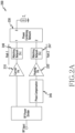
- FIG. 2A illustrates an example of a Doherty power amplifier for describing embodiments of the present disclosure.
- the Doherty power amplifier may indicate a power amplifier structure for improving efficiency of a back-off region through load impedance modulation using two power amplifiers.
- the back-off region may indicate a region having a lower output by a specific value (or offset) in a maximum output region.
- the power amplifier may operate in the back-off region for linear power amplification.
- a Doherty power amplifier (DPA) 200 may include a power divider or a radio frequency (RF) power divider, a first power amplifier 210, a second power amplifier 220, a power combining network 230, a first matching network 240, a phase compensation 245, a second matching network 247, and an output load Z L .
- the DPA 200 may be configured in a structure where the first power amplifier 210 and the second power amplifier 220 are coupled. In so doing, powers divided through the power divider may be inputted to the first power amplifier 210 and the second power amplifier 220.
- the power divider may divide a signal received from an input end.
- the power divider may be a Wilkinson power divider.
- the first power amplifier 210 may be referred to as a main power amplifier (PA), a main amplifier, or a carrier PA.
- the second power amplifier 220 may be referred to as an auxiliary PA, an auxiliary amplifier, or a peaking PA.
- the first power amplifier 210 may be configured with a class-AB biased power amplifier
- the second power amplifier 220 may be configured with a class-C biased power amplifier.
- the first matching network 240 may indicate a configuration for load modulation.
- the first matching network 240 may be a transmission line.
- the transmission line may be R opt in characteristic impedance, and 90° in electrical length.
- an input end of the second power amplifier 220 may be coupled with the phase compensation 245.
- the phase compensation 245 may indicate a configuration for shifting a phase of the signal.
- the phase compensation 245 may indicate a transmission line.
- the transmission line may be 90° in electrical length.
- the second matching network 247 may be coupled to an output end of the second power amplifier 220.
- the second matching network 247 may indicate a transmission line.
- the second matching network 247 may be the transmission line for delivering a signal without changing signal characteristics.
- the power combining network 230 may connect the first path and the second path, and an output end of the Doherty power amplifier 200.
- the connection of the power combining network 230 between the first path and the second path, and the output end of the Doherty power amplifier 200 may indicate an electrical connection, which may indicate either a direct connection or an indirect connection. Specific examples of the coupling of the power combining network 230 shall be described in FIG. 2B .
- FIG. 2B illustrates an example of the power combining network for describing embodiments of the present disclosure.
- the power combining network may indicate the power combining network 230 of FIG. 2A .
- the power combining network may indicate a structure for electrically connecting a first path connected to an output end of a main power amplifier of the Doherty power amplifier and a second path connected to an output end of an auxiliary power amplifier, and the output end of the Doherty power amplifier.
- a point connected with the first path in the power combining network is referred to as a first end or port
- a point connected with the second path is referred to as a second end or port
- a point connected with the output end of the Doherty power amplifier is referred to as a third end or port.
- the power combining network 230 may include a power combining network 231 according to current summing, and a power combining network 232 according to voltage summing.
- the power combining network 230 may combine a plurality of inputted power and output a single power. For example, considering the Doherty power amplifier of FIG. 2A , an output power of the first power amplifier 210 and an output power of the second power amplifier 220 may be combined and outputted as one power.
- the power combining network 231 may combine the first end, the second end and the third end at one node, and be configured to apply the same voltage V.
- a current inputted through the first end in the first path is I 0
- a current inputted through the second end in the second path is ⁇ I 0
- a current outputted through the third end may be (1+ ⁇ )I 0
- effective power of the first end is P 0
- effective power of the second end is ⁇ P 0
- effective power of the third end may be (1+ ⁇ )P 0
- ⁇ denotes a ratio to a reference.
- impedance terminated at the third end is Z L
- input impedance of the first end may be ( ⁇ +1)Z L
- input impedance of the second end may be ( ⁇ +1) ⁇ -1 Z L .
- the power combining network 232 may electrically connect the first end, the second end and the third end through a plurality of transformers.
- FIG. 2B describes the power combining network 232 including ideal transformers by way of example for the sake of explanation.
- a current outputted through the third end is I
- a turns ratios of each of the transformers may be determined to make the current inputted through the first end in the first path NI, and the current inputted through the second end in the second path N ⁇ I.
- the transformer between the first end and the third end is a first transformer
- the transformer between the second end and the third end is a second transformer
- the turns ratio of the first transformer may be 1:N
- the turns ratio of the second transformer may be 1:N ⁇
- the voltage of the third end may be N(1+ ⁇ )V 0
- effective power of the first end is P 0
- effective power of the second end is ⁇ P 0
- effective power of the third end may be (1+ ⁇ )P 0 .
- ⁇ denotes the ratio to the reference.
- the input impedance of the first end may be N -2 ( ⁇ +1) -1 Z L
- the input impedance of the second end may be N -2 ( ⁇ +1) -1 ⁇ Z L .
- the power amplifiers (e.g., the main power amplifier, the auxiliary power amplifier) of the Doherty power amplifier and the output end of the Doherty power amplifier may be connected through the power combining network 230.
- the power amplifiers (e.g., the main power amplifier, the auxiliary power amplifier) of the Doherty power amplifier and the output end of the Doherty power amplifier may be directly connected through the power combining network 231 according to the current summing, and may be indirectly connected through the power combining network 232 according to the voltage summing.
- the connection through the power combining network 230 may indicate the electrical connection.
- the power combining network 230 may output the plurality of the inputted powers as one power.
- FIG. 2C is a graph illustrating examples of power added efficiency (PAE) of power amplifiers based on an output signal according to embodiments of the present disclosure.
- a graph 250 shows a first line 260 showing the PAE based on the power of the output signal of the class-AB power amplifier, a second line 270 showing the PAE based on the power of the output signal of the DPA, and a third line 280 showing the PAE based on the power of the output signal of the DPA using the common mode of the present disclosure.
- a horizontal axis of the graph 250 may indicate the power (unit: dBm) of the output signal, and a vertical axis may indicate the PAE (unit : %).
- the first line 260 may have a maximum PAE value at power P SAT saturated at a maximum output of the outputted signal. However, it is required to back off by a specific value in consideration of the PAPR to achieve linearity of the power amplifier, as described above. However, the PAE is significantly reduced in the region backed off from P SAT by about 6dB.
- the second line 270 may have the maximum PAE value at P SAT , in the same manner as the first line 260.
- the second line 270 has a similar value to the PAE at P SAT even in the region backed off about 6dB, unlike the first line 260, and the efficiency may be generated high.
- the PAE of the second line 270 noticeably decreases.
- the PAE of the second line 270 may be formed lower than the PAE of 6dB.
- the modulation signal using a high-order modulation scheme may be increased in the PAPR, and a conventional Doherty power amplifier (e.g., the Doherty power amplifier 200 of FIG. 2A ) may linearly amplify a signal having a high PAPR (over 6dB) and limit the capability of improving the amplifier efficiency.
- a conventional Doherty power amplifier e.g., the Doherty power amplifier 200 of FIG. 2A
- the Doherty power amplifier 200 of FIG. 2A may linearly amplify a signal having a high PAPR (over 6dB) and limit the capability of improving the amplifier efficiency.
- the third line 280 may have the maximum PAE value at P SAT , in the same manner as the first line 260.
- high efficiency having the same value as the PAE at P SAT even in the back-off region over about 6dB may be generated.
- the Doherty power amplifier e.g., the Doherty power amplifier 300 of FIG. 3
- the impedance modulation of the present disclosure may provide high efficiency in the back-off region (over about 6dB) retaining the linearity.
- the wireless communication system may adopt the modulation schemes for providing greater data capacity.
- modulation schemes may require high PAPR.
- the Doherty power amplifier 200 of FIG. 2A improves the efficiency only in the back-off region of about 6dB, compared to the class-AB bias power amplifier, and may be limited in the efficiency improving capability with respect to the modulation signals having high PAPR.
- the present disclosure suggests a Doherty power amplifier (hereafter, a Doherty power amplifier using a common mode) for adjusting the back-off region to provide an improved efficiency, by using a common mode through a configuration which interconnects power amplifiers of the Doherty power amplifier.
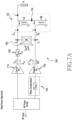
- FIG. 3 illustrates an example of a Doherty power amplifier using a common mode according to an embodiment of the present disclosure.
- a Doherty power amplifier 300 may include a power divider or an RF power divider, a first power amplifier 310, a second power amplifier 320, a power combining network 330, a first matching network 340, a phase compensation 345, a second matching network 347, and a common mode network 350.
- the first power amplifier 310 may be referred to as a main PA, a main amplifier or a carrier PA.
- the second power amplifier 320 may be referred to as an auxiliary PA, an auxiliary amplifier, or a peaking PA.
- the first power amplifier 310 may amplify power with respect to a signal (e.g., an RF signal) divided and inputted from the power divider.
- the first power amplifier 310 may provide the amplified output signal to the power combining network 330 via the first matching network 340.
- a path connecting the node A and a first end or port of the power combining network 330 may be referred to as a first path.
- the second power amplifier 320 may receive a signal which is divided and inputted from the power divider and compensated in phase through the phase compensation 345.
- the second power amplifier 320 may amplify power of the inputted signal and provide it to the power combining network 330 via the second matching network 347.
- a path connecting the node B and a second end or port of the power combining network 330 may be referred to as a second path.
- the first power amplifier 310 may be configured with a class-AB power amplifier.
- the second power amplifier 320 may be configured with a class-C power amplifier.
- the power combining network 330 may indicate a structure for interconnecting a first end, a second end and a third end.
- the first end may be connected to the first path which is extended from the first power amplifier 310 and interconnects the first matching network 340 and the node A.
- the second end may be connected to the second path which is extended from the second power amplifier 320 and interconnects the second matching network 347 and the node B.
- the third end may indicate an output end of the Doherty power amplifier 300, and the output end of the Doherty power amplifier 300 may be connected with load having impedance Z L .
- the power combining network 330 may include a power combining network using current summing and a power combining network using voltage summing, as explained in FIG. 2B . Details thereof shall be described in FIGS. 5A and 5B .
- the first matching network 340 may indicate a configuration for load modulation.
- the first matching network 340 may be a transmission line.
- the first matching network 340 may be referred to as a first transmission line.
- the first matching network 340 may be configured with characteristics of a specific condition.
- the phase compensation 345 may indicate a configuration for compensating for a phase difference between the first power amplifier 310 and the second power amplifier 320.
- the phase compensation 345 may be a transmission line.
- the phase compensation 345 may be referred to as a second transmission line.
- the second matching network 347 may indicate a configuration for the load modulation.
- the second matching network 347 may be a transmission line. However, it may be the transmission line for delivering the signal without changing characteristics of the signal outputted from the second power amplifier 320, to ease explanation in the present disclosure.
- the second matching network 347 may not be depicted.
- the present disclosure is not limited thereto, and the second matching network 347 may be configured with characteristics of a specific condition for the sake of more precise impedance matching.
- the common mode network 350 may be an arbitrary reactance element.
- the common mode network 350 may be the element having an impedance value of jX.
- j may denote an imaginary unit
- X may denote a random constant.
- the common mode network 350 may be a capacitor or an inductor which is a lumped element as described in FIG. 4B , and may be a transmission line which is a distributed element substantially operating as the capacitor or the inductor in a high frequency signal.
- the common mode network 350 may include a combination of the lumped element and the distributed element. Descriptions on the common mode characteristic and the structure of the common mode network 350 shall be elucidated in FIGS. 4A and 4B .
- the common mode network 350 may be disposed between the node A and the node B.
- the common mode network 350 may be disposed on the third path.
- the common mode network 350 may electrically separate the first path and the second path under a specific condition through the common mode characteristic, to be described.
- the common mode network 350 may build an electrical wall to electrically open the third path. Details thereof shall be explained in FIG. 4A .
- FIG. 4A illustrates an example for describing a common mode characteristic of a common mode network according to embodiments of the present disclosure.
- a common mode network 450 of FIG. 4A may be understood in the same manner as the common mode network 350 of FIG. 3 .
- FIG. 4A depicts connections between the common mode network 450 and adjacent nodes (e.g., a node A and a node B), and other connections are omitted to ease description.
- the common mode network 450 is depicted in a diagram 400 and a diagram 405 disposed between the node A and the node B.
- the diagram 400 and the diagram 405 may be electrically identical equivalent circuits.
- an S parameter of the common mode network 450 is S COM
- voltage of the node A is V 0
- voltage of the node B is V 0
- current flowing from the node A to the common mode network 450 is I 0
- current flowing from the node B to the common mode network 450 is I 0 .
- An arbitrary circuit may build an electrical wall which blocks current in a symmetric plane between two symmetric nodes.
- the common mode network 450 may be divided into two configurations having S parameter of S COM '.
- the common mode network 450 may be configured in the symmetric structure between the node A and the node B.
- the electrical wall may be built and divided into two identical networks.
- a structure of a Doherty power amplifier for improving efficiency in a wider back-off region, by dividing into different paths based on such characteristics, is described, in FIGS. 5A , 5B , 6A , 6B , 7A , 7B , 8A , 8B , 8C , and 9 .
- FIG. 4B illustrates examples of the structure of the common mode network according to embodiments of the present disclosure.
- FIG. 4B illustrates various examples for configuring the common mode network 450.
- the common mode network of the Doherty power amplifier using the common scheme according to embodiments of the present disclosure is not interpreted only in the structures shown in FIG. 4B . That is, a configuration having the electrically same meaning may be understood as an embodiment of the present disclosure.
- the common mode network 450 may include a lumped element.
- the common mode network 450 may include a capacitor 452 with capacitance C.
- the common mode network 450 may include an inductor 454 with inductance L.
- the common mode network 450 may include a combination of a capacitor and an inductor, which is not depicted.
- the common mode network 450 may include a distributed element.
- the common mode network 450 may include a transmission line 456.
- the transmission line may be configured with the characteristic impedance of Z 0 and the electrical length of ⁇ °.
- the common mode network 450 may include a combination of a lumped element and a distributed element.
- the common mode network 450 may include a combination 458 of a capacitor and transmission lines.
- the common mode network 450 may include a combination 460 of an inductor and transmission lines.
- the common mode network 450 may include at least one of a lumped element or a distributed element, as shown in FIG. 4B .
- the common mode network 450 may be configured, through a combination of at least one capacitor, at least one inductor, or at least one transmission line.
- FIG. 5A illustrates an example of coupling between output ends of power amplifiers of a Doherty power amplifier using a common mode according to embodiments of the present disclosure.
- the Doherty power amplifier of FIG. 5A includes a power combining network according to current summing.
- FIG. 5A illustrates the example of the Doherty power amplifier including the power combining network 231 of FIG. 2B .
- the power combining network according to the current summing is referred to as a first power combining network.
- a Doherty power amplifier 500 may include a power divider or RF power divider, a first power amplifier 510, a second power amplifier 520, a first power combining network 530, a first matching network 540, a phase compensation 545, and a common mode network 550.
- the first power amplifier 510 may be referred to as a main PA, a main amplifier or a carrier PA.
- the second power amplifier 520 may be referred to as an auxiliary PA, an auxiliary amplifier or a peaking PA.
- the first power amplifier 510 may amplify power with respect to a signal (e.g., an RF signal) divided and inputted from the power divider.
- the first power amplifier 510 may provide the amplified output signal to the first power combining network 530 via the first matching network 540.
- a path connecting the node A and a first end or port of the first power combining network 530 may be referred to as a first path.
- the second power amplifier 520 may receive a signal which is divided and inputted from the power divider and compensated in phase through the phase compensation 545.
- the second power amplifier 520 may amplify power of the inputted signal and provide it to the first power combining network 530.
- a path connecting the node B and a second end or port of the first power combining network 530 may be referred to as a second path.
- the first power amplifier 510 may be configured with a class-AB power amplifier.
- the second power amplifier 520 may be configured with a class-C power amplifier.
- the first power combining network 530 may include a combining circuit 531 and a first impedance matching circuit 533 and a second impedance matching circuit 535.
- the combining circuit 531 may indicate a structure for interconnecting a first end, a second end and a third end at one node.
- the first end may be connected to the first path which is extended from the first power amplifier 510 and interconnects the first matching network 540, the node A and the first impedance matching circuit 533.
- the second end may be connected to the second path which is extended from the second power amplifier 520 and interconnects the node B and the second impedance matching circuit 535.
- the third end may indicate an output end of the Doherty power amplifier 500, and the output end of the Doherty power amplifier 500 may be connected with load of impedance R L .
- the first impedance matching circuit 533 and the second impedance matching circuit 535 may indicate a transmission line for making voltage V A of the node A and voltage V B of the node B the same.
- FIG. 5A illustrates, to ease the explanation, the first impedance matching circuit 533 as the transmission line having characteristic impedance of Z C and the electrical length of 90°, and the second impedance matching circuit 535 as the transmission line having characteristic impedance of Z P and the electrical length of 90°.
- the first power combining network 530 which is the current summing power combining network may include a combining network 531 for connecting the first end and the second end connected with the power amplifiers with the output end.
- the first power combining network 530 may include the first impedance matching circuit 533 and the second impedance matching circuit 535 for making the potential difference of nodes (e.g., the node A and the node B) between the paths (e.g., the first path, the second path) extended from the output end of the power amplifiers zero.
- the first matching network 540 may indicate a configuration for the load modulation.
- the first matching network 540 may be a transmission line.
- the first matching network 540 may be referred to as a first transmission line.
- the first matching network 540 may be configured with characteristics of a specific condition.
- the first matching network 540 may be a transmission line having the characteristic impedance R opt , and the electrical length ⁇ offset °.
- the phase compensation 545 may indicate a configuration for compensating for a phase difference between the first power amplifier 510 and the second power amplifier 520.
- the phase difference between the first power amplifier 510 and the second power amplifier 520 may indicate a phase difference occurred according to the first matching network 504.
- the phase compensation 545 may be a transmission line.
- the phase compensation 545 may be referred to as a second transmission line.
- the phase compensation 545 may be the transmission line of the electrical length ⁇ offset ° to compensate for the phase difference.
- the common mode network 550 may be an arbitrary reactance element.
- the common mode network 550 may be the element having an impedance value of jX.
- j may denote an imaginary unit
- X may denote a random constant.
- the common mode network 550 may be a capacitor or an inductor which is a lumped element, and may be a transmission line which is a distributed element substantially operating as the capacitor or the inductor in a high frequency signal.
- the common mode network 550 may include a combination of a lumped element and a distributed element.
- the common mode network 550 may be disposed between the node A and the node B.
- the common mode network 550 may be disposed on the third path.
- the common mode network 550 may electrically separate the first path and the second path under a specific condition through the common mode characteristic.
- the specific condition may indicate that the potential of the node A and the node B is identical, the magnitude of the current is identical, but the phases are opposite (i.e., current of opposite directions).
- the common mode network 550 may build an electrical wall to electrically open the third path.
- FIG. 5B illustrates another example of coupling between the output ends of the power amplifiers of the Doherty power amplifier using the common mode according to embodiments of the present disclosure.
- the Doherty power amplifier of FIG. 5B includes a power combining network according to voltage summing.
- FIG. 5B illustrates the example of the Doherty power amplifier including the power combining network 232 of FIG. 2B .
- the power combining network according to the voltage summing is referred to as a second power combining network.
- the Doherty power amplifier 500 may include the power divider or RF power divider, the first power amplifier 510, the second power amplifier 520, a second power combining network 532, the first matching network 540, the phase compensation 545, and the common mode network 550.
- the first power amplifier 510 may be referred to as the main PA, the main amplifier or the carrier PA.
- the second power amplifier 520 may be referred to as the auxiliary PA, the auxiliary amplifier or the peaking PA.
- the first power amplifier 510 may amplify power with respect to a signal (e.g., an RF signal) divided and inputted from the power divider.
- the first power amplifier 510 may provide the amplified output signal to the second power combining network 532 via the first matching network 540.
- a path connecting the node A and a first end or port of the second power combining network 532 may be referred to as a first path.
- the second power amplifier 520 may receive a signal which is divided and inputted from the power divider and compensated in phase through the phase compensation 545.
- the second power amplifier 520 may amplify power of the inputted signal and provide it to the second power combining network 532.
- a path connecting the node B and a second end or port of the second power combining network 532 may be referred to as a second path.
- the first power amplifier 510 may be configured with a class-AB power amplifier.
- the second power amplifier 520 may be configured with a class-C power amplifier.
- the second power combining network 532 may include a plurality of transformers.
- the second power combining network 532 may include a first transformer interconnecting a first end and a third end and a second transformer interconnecting a second end and the third end.
- the first end may be connected to the first path which is extended from the first power amplifier 510 and interconnects the first matching network 540 and the node A.
- the second end may be connected to the second path which is extended from the second power amplifier 520 and connects the node B.
- the third end may indicate the output end of the Doherty power amplifier 500, and the output end of the Doherty power amplifier 500 may be connected with output the impedance R L .
- the plurality of the transformers of the second power combining network 532 may be configured with a turns ratio for making the voltage V A of the node A and voltage V B of the node B the same.
- the turns ratio of the first transformer and the turns ratio of the second transformer distinguished based on a node 534 may be different from each other.
- the second power combining network 532 which is the voltage summing power combining network may not include the first impedance matching circuit 533 and the second impedance matching circuit 535 unlike the first power combining network 530. This is because the second power combining network 532 may design the potential difference 0 of the node A and the node B based on the turns ratios of the first transformer and the second transformer.
- the transformers of the power combining network 532 may be configured with transmission lines. That is, the transformers may be configured according to electromagnetic induction of adjacent transmission lines.
- the transmission line may be twisted (i.e., spiral) to form the transformer, and the turns ratio may differ depending on the twist degree.
- the first matching network 540 may indicate the configuration for the load modulation.
- the first matching network 540 may be a transmission line.
- the first matching network 540 may be referred to as a first transmission line.
- the first matching network 340 may be configured with characteristics of a specific condition.
- the first matching network 540 may be the transmission line having the characteristic impedance R opt , and the electrical length ⁇ offset °.
- the phase compensation 545 may indicate the configuration for compensating for a phase difference between the first power amplifier 510 and the second power amplifier 520.
- the phase difference between the first power amplifier 510 and the second power amplifier 520 may indicate a phase difference occurred according to the first matching network 540.
- the phase compensation 545 may be a transmission line.
- the phase compensation 545 may be referred to as a second transmission line.
- the phase compensation 545 may be the transmission line of the electrical length ⁇ offset ° to compensate for the phase difference.
- the common mode network 550 may be an arbitrary reactance element.
- the common mode network 550 may be the element having the impedance value of jX.
- j may denote the imaginary unit
- X may denote the random constant.
- the common mode network 550 may be a capacitor or an inductor which is the lumped element, and may be a transmission line which is the distributed element substantially operating as the capacitor or the inductor in the high frequency signal.
- the common mode network 550 may include a combination of a lumped element and a distributed element.
- the common mode network 550 may be disposed between the node A and the node B.
- the common mode network 550 may be disposed on the third path.
- the common mode network 550 may electrically separate the first path and the second path under a specific condition through the common mode characteristic.
- the specific condition may indicate that the potential of the node A and the node B is identical, the magnitude of the current is identical, but the phases are opposite (i.e., current of opposite directions).
- the common mode network 550 may build an electrical wall to electrically open the third path.
- FIG. 6A illustrates an example of operations of a Doherty power amplifier using a common mode in a first state according to embodiments of the present disclosure.
- FIG. 6B illustrates an example of operations of the Doherty power amplifier using the common mode in a second state according to embodiments of the present disclosure.
- a Doherty power amplifier 600 of FIG. 6A and a Doherty power amplifier 605 of FIG. 6B may be understood in the same manner as the Doherty power amplifier 500 of FIG. 5A .
- details on structures of the Doherty power amplifier 600 and the Doherty power amplifier 605 may be understood in the same manner as the Doherty power amplifier 500 of FIG. 5A .
- an operation process of the Doherty power amplifier 600 of the first state and the Doherty power amplifier 605 of the second state shall be described, and the same description as the description in FIG. 5A is omitted.
- the first state may indicate a high power (HP) state
- the second state may indicate a low power (LP) state.
- the HP and the LP may be determined relatively based on maximum output power.
- the HP i.e., the first state
- the LP i.e., the second state
- the HP may indicate the maximum output power.
- the LP i.e., the second state
- the HP may indicate a power region lower than the maximum output power and with no power output from the auxiliary amplifier.
- the Doherty power amplifier 600 may include a power divider or RF power divider, a first power amplifier 610, a second power amplifier 620, a first power combining network 630, a first matching network 640 (i.e., a first transmission line), a phase compensation 645 (i.e., a second transmission line) and a common mode network 650.
- an output power magnitude ratio of the first power amplifier 610 of the Doherty power amplifier 600 and the second power amplifier 620 of the Doherty power amplifier 600 may be defined as 1: ⁇ .
- ⁇ may indicate a ratio of the power to reference power (e.g., the output power of the first power amplifier).
- ⁇ may be 1.
- ⁇ may be a value smaller than 1 or greater than 1.
- optimal load impedance of the first power amplifier 610 and the second power amplifier 620 may be determined to R opt and R opt / ⁇ in the first state.
- the first matching network 640 may be a transmission line having the characteristic impedance R opt , and the electrical length ⁇ offset °.
- the phase compensation 645 may be a transmission line in the electrical length ⁇ offset °, to compensate for a phase difference occurred by the first matching network 640.
- a relationship between a first impedance matching circuit 633 and a second impedance matching circuit 635 is given by the following Equation 1.
- Z C may denote characteristic impedance of the first impedance matching circuit 633
- Z P may denote characteristic impedance of the second impedance matching circuit 635
- ⁇ may denote an output power ratio of the first power amplifier 610 and the second power amplifier 620 in the first state
- R L may denote load impedance connected to the output end of the Doherty power amplifier 600
- R opt may denote optimal load impedance of the first power amplifier 610 in the first state.
- R L and R opt are assumed to be the impedance including only resistance component to ease calculation.
- the common mode network 650 may build an electrical wall. Since the common mode network 650 operates as the configuration which does not electrically exist, the output end of the first power amplifier 610 and the output end of the second power amplifier 620 (i.e., the first path and the second path) may be separated.
- the optimal load impedance R opt may be applied to the output end of the first power amplifier 610, and the optimal load impedance ⁇ -1 R opt may be applied also to the output end of the second power amplifier 620.
- the Doherty power amplifier 600 may output optimal power in the first state.
- the second power amplifier 620 of the Doherty power amplifier 600 may be controlled not to operate. If the second power amplifier 620 does not operate, the impedance from a perspective of the output end of the second power amplifier 620 may be infinite ⁇ . In the second state, the output power of the first power amplifier 610 may be reduced to k -1 P 0 . In this case, impedance Z c ' viewed as the load at the node A may be given by the following equation .
- Z C ′ ⁇ + 1 ⁇ 1 R opt + j ⁇ 2 ⁇ + 1 ⁇ 2 X
- Z c ' may denote impedance viewed as the load at the node A in the second state
- ⁇ may denote the power ratio of the first power amplifier 610 and the second power amplifier 620
- j may denote the imaginary unit
- X may denote reactance of the common mode network 650
- R opt may denote the optimal load impedance of the first power amplifier 610 in the first state.
- Z C ' may be calculated according to an equivalent circuit (or port network system analysis) viewing the node A.
- the optimal load impedance of the output end of the first power amplifier 610 may be determined to a value kR opt increased (i.e., modulated) by k times.
- the first matching network 640 may satisfy an impedance transformation relationship based on the following equation to provide the optimal load impedance for the output end of the first power amplifier 610.
- Z C ′ * R opt 1 + jk tan ⁇ offset ° k + j tan ⁇ offset °
- Z C ' may denote a complex conjugate of the impedance viewed as the load at the node A in the second state
- j may denote the imaginary unit
- k may denote an impedance modulation rate
- R opt may denote the optimal load impedance of the first power amplifier 610 in the first state.
- equations of the reactance component X of the common mode network 650 and the electrical length ⁇ offset ° of the first matching network 640 may be written as the following equations.
- ⁇ may denote the output power ratio of the first power amplifier 610 and the second power amplifier 620 in the first state
- k may denote the impedance modulation rate
- R opt may denote the optimal load impedance of the first power amplifier 610 in the first state.
- the Doherty power amplifier 600 if the Doherty power amplifier 600 is in the first state (HP), the first path extended from the output end of the first power amplifier 610 and the second path extended from the output end of the second power amplifier 620 may be electrically separated by the common mode characteristic of the common mode network 650.
- the optimal load impedance may be applied for the first power amplifier 610 and the second power amplifier 620, by designing the impedance values electrically separated of the first impedance matching circuit 633 and the second impedance matching circuit 635 of the current summing power combining network 630 to meet a specific condition.
- the Doherty power amplifier 600 of the first state may output the maximum output power.
- the second power amplifier 620 may not operate.
- the first matching network 640 and the common mode network 650 may be determined based on the transmission line theory.
- the optimal load impedance for the reduced output power may be modulated at a specific rate (i.e., the modulation rate k), and the back-off region of the Doherty power amplifier 600 for providing the improved efficiency based on the modulation rate may be expanded.
- back-off power P backoff may be given by the following equation with k and ⁇ .
- the back-off power may indicate a difference value between two output power points having maximum efficiency from the maximum output power.
- P backoff dB 10 log k + 10 log ⁇ + 1
- P backoff may denote power indicating a back-off range for improving the efficiency of the Doherty power amplifier
- ⁇ may denote the output power ratio of the first power amplifier 610 and the second power amplifier 620 in the first state
- k may denote a constant indicating the impedance modulation rate.
- the back-off power P backoff of the Doherty power amplifier may be determined by the modulation rate k of the impedance (i.e., the load impedance) viewed from the output end of the first power amplifier of the Doherty power amplifier, and the power ratio ⁇ between the first power amplifier and the second power amplifier.
- k and ⁇ may be determined based on the operation region and the operation state of the power amplifier, in designing the power amplifier.
- the Doherty power amplifier using the common mode may output the maximum output power in the first state of the power amplifier, and achieve high efficiency in the wide back-off region in the second state, using the current summing power combining and the common mode characteristic.
- the power amplifier of the present disclosure may support a signal having a high PAPR required according to a modulation order, and also improve battery efficiency of an electronic device including the power amplifier by minimizing power usage.
- FIG. 7A illustrates another example of operations of a Doherty power amplifier using a common mode in a first state according to embodiments of the present disclosure.
- FIG. 7B illustrates another example of operations of the Doherty power amplifier using the common mode in a second state according to embodiments of the present disclosure.
- a Doherty power amplifier 700 of FIG. 7A and a Doherty power amplifier 705 of FIG. 7B may be understood in the same manner as the Doherty power amplifier 500 of FIG. 5B . Accordingly, details on structures of the Doherty power amplifier 700 and the Doherty power amplifier 705 may be understood in the same manner as the Doherty power amplifier 500 of FIG. 5B .
- an operation process of the Doherty power amplifier 700 of the first state and the Doherty power amplifier 705 of the second state shall be described, and the same description as the description in FIG. 5A is omitted.
- the first state may indicate the HP state
- the second state may indicate the LP state.
- the HP and the LP may be determined relatively based on maximum output power.
- the HP i.e., the first state
- the LP i.e., the second state
- the HP may indicate a maximum output power region.
- the LP i.e., the second state
- the HP may indicate a power region lower than the maximum output power and with no power output from the auxiliary amplifier.
- the Doherty power amplifier 700 may include a power divider or RF power divider, a first power amplifier 710, a second power amplifier 720, a second power combining network 732, a first matching network 740 (i.e., a first transmission line), a phase compensation 745 (i.e., a second transmission line) and a common mode network 750.
- an output power magnitude ratio of the first power amplifier 710 of the Doherty power amplifier 700 and the second power amplifier 720 of the Doherty power amplifier 700 may be defined as 1: ⁇ .
- ⁇ may indicate a ratio of the power against the reference power (e.g., the output power of the first power amplifier 710).
- ⁇ may be 1.
- ⁇ may be a value smaller than 1 or greater than 1.
- optimal load impedance of the first power amplifier 710 and the second power amplifier 720 may be determined to R opt and R opt / ⁇ in the first state.
- the first matching network 740 may be a transmission line having the characteristic impedance R opt , and the electrical length ⁇ offset °.
- the phase compensation 745 may be a transmission line in the electrical length ⁇ offset °, to compensate for a phase difference occurred by the first matching network 740.
- a condition i.e., a potential difference between a node A and a node B is 0
- a turns ratio of a first transformer between a first end and a third end of the second power combining network 732 is set to 1:N
- a turns ratio of a second transformer between a second end and the third end may be set to 1:N ⁇ .
- the first transformer and the second transformer may be distinguished based on a node 734.
- N may denote the turns ratio of the third end to the first end of the first transformer
- ⁇ may denote an output power ratio of the first power amplifier 710 and the second power amplifier 720 in the first state
- R L may denote load impedance connected to an output end of the Doherty power amplifier 700
- R opt may denote optimal load impedance of the first power amplifier 710 in the first state.
- R L and R opt are assumed to be the impedance including only resistance component to ease the calculation.
- the common mode network 750 may build an electrical wall. Since the common mode network 750 operates as the configuration which does not electrically exist, the output end of the first power amplifier 710 and the output end of the second power amplifier 720 (i.e., the first path and the second path) may be separated. As a result, the optimal load impedance R opt may be applied to the output end of the first power amplifier 710, and the optimal load impedance ⁇ -1 R opt may be applied also to the output end of the second power amplifier 720. Hence, the Doherty power amplifier 700 may output optimal power in the first state.
- Z C ' may denote the impedance viewed as the load at the node A in the second state
- ⁇ may denote the output power ratio of the first power amplifier 710 and the second power amplifier 720 in the first state
- j may denote the imaginary unit
- X may denote reactance of the common mode network 750
- R opt may denote the optimal load impedance of the first power amplifier 710 in the first state.
- Z C may be calculated according to an equivalent circuit or port network system analysis.
- the optimal load impedance of the output end of the first power amplifier 710 may be determined to a value kR opt increased (i.e., modulated) by k times.
- equations of the reactance component X of the common mode network 750 and the electrical length ⁇ offset ° of the first matching network 740 may be written as the following equations to provide the optimal load impedance for the output end of the first power amplifier 710.
- ⁇ may denote the output power ratio of the first power amplifier 710 and the second power amplifier 720 in the first state
- k may denote the impedance modulation rate
- R opt may denote the optimal load impedance of the first power amplifier 710 in the first state.
- the Doherty power amplifier 700 if the Doherty power amplifier 700 is in the first state (HP), the first path extended from the output end of the first power amplifier 710 and the second path extended from the output end of the second power amplifier 720 may be electrically separated by the common mode characteristic of the common mode network 750.
- the optimal load impedance may be applied for the first power amplifier 710 and the second power amplifier 720, by designing the first transformer and the second transformer electrically separated of the current summing power combining network 732 to meet a specific condition.
- the Doherty power amplifier 700 of the first state may output the maximum output power.
- the second power amplifier 720 may not operate.
- the first matching network 740 and the common mode network 750 may be determined based on the transmission line theory.
- the optimal load impedance for the reduced output power may be modulated at a specific ratio (i.e., the modulation rate k), and the back-off region of the Doherty power amplifier 700 for providing the improved efficiency based on the modulation rate may be expanded.
- back-off power P backoff may be given by the following equation with k and ⁇ .
- the back-off power may indicate a difference value between two output power points having maximum efficiency from the maximum output power.
- the Doherty power amplifier using the common mode may output the maximum output power in the first state of the power amplifier, and achieve high efficiency in the wide back-off region in the second state, using the voltage summing power combining and the common mode characteristic.
- the power amplifier of the present disclosure may support a signal having a high PAPR required according to the modulation order, and also improve battery efficiency of an electronic device including the power amplifier by minimizing power usage.
- FIG. 8A is a graph illustrating examples of load impedance of a power amplifier based on input voltage according to embodiments of the present disclosure.
- the input voltage of FIG. 8A indicates the load impedance based on the magnitude of the voltage applied to the input end of each power amplifier (e.g., the first power amplifier 310 and the second power amplifier 320 of the Doherty power amplifier 300 of FIG. 3 or the first power amplifier 610 and the second power amplifier 620 of the Doherty power amplifier 600 of FIG. 6A and FIG. 6B or the first power amplifier 710 and the second power amplifier 720 of the Doherty power amplifier 700 of FIG. 7A and FIG. 7B ).
- a first power amplifier or a main amplifier, a carrier amplifier
- a second power amplifier or an auxiliary amplifier, a peaking amplifier
- a graph 800 includes solid lines showing a load impedance value based on the input voltage for the first power amplifier (i.e., a carrier PA), and dotted lines showing a load impedance value based on the input voltage for the second power amplifier (i.e., a peaking PA).
- the graph 800 may show a first line 810 showing the first power amplifier if k (the modulation rate of the load impedance of the amplifier) is 2, a second line 820 showing the first power amplifier if k is 3, and a third line 830 showing the first power amplifier if k is 4.
- a horizontal axis of the graph 800 may indicate the voltage (unit : V) of the input end voltage of the amplifier, and a vertical axis may indicate the load impedance (unit: ⁇ ).
- the load impedance may be generated at about R opt value.
- the load impedance may be converged onto about 2R opt value.
- a timing where the load impedance begins to converge may be the input voltage magnitude about V IN, MAX /2 of the first power amplifier.
- the load impedance may be generated at about R opt value similarly to the first power amplifier.
- the load impedance may be converged to the infinity ⁇ . That is, comparing the first line 810 and the fourth line 815, if the Doherty power amplifier according to embodiments of the present disclosure is in the first state (i.e., the HP state), the first power amplifier and the second power amplifier of the Doherty power amplifier both may be formed with the load impedance of about R opt value.
- the Doherty power amplifier according to embodiments of the present disclosure is in the second state (i.e., the LP state)
- the first power amplifier of the Doherty power amplifier may be formed with the load impedance of about 2R opt value
- the second power amplifier may be formed with the load impedance of the infinity ⁇ .
- the load impedance may be generated at about R opt value.
- the load impedance may be converged onto about 3R opt value.
- the load impedance may begin to converge if the input voltage magnitude of the first power amplifier is a value between about V IN, MAX /2 and about V IN, MAX /4.
- the load impedance may be generated at about R opt value similarly to the first power amplifier.
- the load impedance may be converged to the infinity ⁇ . That is, comparing the second line 820 and the fifth line 825, if the Doherty power amplifier according to embodiments of the present disclosure is in the first state (i.e., the HP state), the first power amplifier and the second power amplifier of the Doherty power amplifier both may be formed with the load impedance of about R opt value.
- the Doherty power amplifier according to embodiments of the present disclosure is in the second state (i.e., the LP state)
- the first power amplifier of the Doherty power amplifier may be formed with the load impedance of about 3R opt value
- the second power amplifier may be formed with the load impedance of the infinity ⁇ .
- the load impedance may be generated at about R opt value.
- the load impedance may be converged onto about 4R opt value. At this time, the load impedance may begin to converge if the input voltage magnitude of the first power amplifier is about V IN, MAX /4.
- the load impedance may be generated at about R opt value similarly to the first power amplifier.
- the load impedance may be converged to the infinity ⁇ . That is, comparing the third line 830 and the sixth line 835, if the Doherty power amplifier according to embodiments of the present disclosure is in the first state (i.e., the HP state), the first power amplifier and the second power amplifier of the Doherty power amplifier both may be formed with the load impedance of about R opt value.
- the Doherty power amplifier according to embodiments of the present disclosure is in the second state (i.e., the LP state)
- the first power amplifier of the Doherty power amplifier may be formed with the load impedance of about 4R opt value
- the second power amplifier may be formed with the load impedance of the infinity ⁇ .
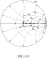
- FIG. 8B is a graph illustrating an example of load impedance change of the first power amplifier based on the input voltage according to embodiments of the present disclosure.
- a third line 855 showing the load impedance change of the first power amplifier if k is 4 are shown.
- the load impedance of the first power amplifier may be formed as a value between R opt in the first state (i.e., HP) and 2R opt in the second state (i.e., LP).
- the load impedance of the first power amplifier may be formed as a value between R opt in the first state and 3R opt in the second state.
- the load impedance of the first power amplifier may be formed as a value between R opt in the first state and 4R opt in the second state.
- the first line 851 through the third line 855 may determine the range of the load impedance according to the k value. Within the determined range, the load impedance may determine the load impedance value based on the power amplifier state, that is, the output power magnitude. In addition, the back-off region improved in efficiency may be determined according to the modulation rate k of the load impedance.
- FIG. 8C is a graph illustrating an example of load impedance change of the second power amplifier based on the input voltage according to embodiments of the present disclosure.
- a third line 865 showing the load impedance change of the second power amplifier if k is 4 are shown.
- the load impedance of the second power amplifier may be generated as a value between R opt in the first state (i.e., HP) and ⁇ in the second state (i.e., LP).
- the first line 861 may be formed in a straight line of which the phase value is fixed to zero.
- the load impedance of the second power amplifier may be formed as a value between R opt in the first state to ⁇ in the second state.
- the load impedance of the second power amplifier may be formed as a value between R opt in the first state to ⁇ in the second state.
- the third line 865 may be formed in a curved line of which the phase value changes, and may be formed with the greater phase value change than the second line 863.
- the reactance of the common scheme network is capacitive, and the load impedance of the second power amplifier may have a positive reactance value opposite to the reactance of the common mode network. That is, the load impedance of the second power amplifier may change with the positive phase value.
- a fourth line 871 showing the load impedance change of the second power amplifier if the modulation rate k for the load impedance is 2
- a fifth line 873 showing the load impedance change of the second power amplifier if k is 3
- a sixth line 875 showing the load impedance change of the second power amplifier if k is 4
- the load impedance of the second power amplifier may be formed as a value between R opt in the first state (i.e., HP) and ⁇ in the second state (i.e., LP).
- the fourth line 871 may be formed in a straight line of which the phase value is fixed to zero.
- the load impedance of the second power amplifier may be formed as a value between R opt in the first state to ⁇ in the second state.
- the fifth line 873 may be formed in a curved line of which the phase value changes.
- the load impedance of the second power amplifier may be formed as a value between R opt in the first state to ⁇ in the second state.
- the sixth line 875 may be formed as a curved line of which the phase value changes, and may be formed with the greater phase value change than the fifth line 873.
- the reactance of the common stage network is inductive, and the load impedance of the second power amplifier may have a negative reactance value opposite to the reactance of the common mode network. That is, the load impedance of the second power amplifier may change with the negative phase value.
- the Doherty power amplifier using the common mode may output the maximum output power in the first state of the power amplifier, using the voltage summing power combining and the common mode characteristic.
- the power amplifier may achieve the wide back-off region by adjusting the modulation rate of the load impedance in the second state.
- the modulation rate of the load impedance may be related to the common mode network and the first matching network. As the modulation rate of the load impedance is adjusted, the back-off power value may be adjusted.
- the change of the PAE based on the modulation rate change shall be explained in FIG. 9 .
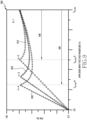
- FIG. 9 is a graph illustrating an example of PAE based on an input voltage of a Doherty power amplifier using a common mode according to embodiments of the present disclosure.
- a horizontal axis of a graph 900 indicates the magnitude (unit: V) of the input voltage of the amplifier, and a vertical axis indicate the PAE (unit : %).
- a third line 930 indicating the PAE change if k is 4 are shown.
- the PAE may be generated at about 80%.
- the PAE may be generated at about 80% similarly to the maximum magnitude of the input voltage.
- the PAE may be generated at about 80%.
- the PAE may be generated at about 80%.
- the load impedance value may be adjusted.
- the value at which the load impedance of the first power amplifier is converged by the modulation rate may be determined.
- modulating the load impedance of the amplifier may indicate that the modulation rate is adjustable and the back-off power region value of the improved efficiency is adjustable. That is, amplifier performance may be improved by expanding the high-efficiency back-off region of the amplifier.
- the Doherty power amplifier using the common scheme according to embodiments of the present disclosure may have the expanded high-efficiency back-off region, unlike a conventional amplifier structure (e.g., class-AB, Doherty power amplifier).
- the Doherty power amplifier using the common scheme according to embodiments of the present disclosure may be the structure which arranges the common mode network interconnecting the first path extended from the output end of the first power amplifier (or the main amplifier, the carrier amplifier) and the second path extended from the output end of the second power amplifier (or the auxiliary amplifier, the peaking amplifier).
- the Doherty power amplifier of the present disclosure may be designed to electrically separate the first path and the second path using the common mode characteristic of the common mode network in the first state (i.e., the HP state), and to apply the optimal load impedance for each power amplifier, thus output the maximum output power in the first state of the power amplifier.
- the Doherty power amplifier of the present disclosure may determine the modulation rate of the load impedance by adjusting the element value of the transmission line (i.e., the first matching network) connected to the common mode network and the output end of the first power amplifier in the second state (i.e., the LP state), and accordingly achieve a wider back-off region improved in the efficiency.
- the power amplifier of the present disclosure may be used in a signal of a modulation scheme having high PAPR according to development of a wireless communication system, and minimize the power consumption.
- an electronic device e.g., a base station, a terminal, etc.
- the Doherty power amplifier structure may minimize power consumption, reduce heating, and increase battery lifetime.
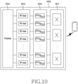
- FIG. 10 illustrates a functional configuration of an electronic device according to various embodiments of the present disclosure.
- An electronic device 1010 may be one of a base station or a terminal. According to an embodiment, the electronic device 1010 may be a a massive MIMO unit (MMU) or a mmWave device.
- MMU massive MIMO unit
- the electronic device 1010 may include an antenna unit 1011, a filter unit 1012, an RF processing unit 1013, and a control unit 1014.
- the antenna unit 1011 may include a plurality of antennas.
- the antenna performs functions for transmitting and receiving signals over a radio channel.
- the antenna may include a conductive formed on a substrate (e.g., a printed circuit board (PCB)) or a radiator formed in a conductive pattern.
- the antenna may radiate an upconverted signal or obtain a signal radiated by other device over the radio channel.
- Each antenna may be referred to as an antenna element or an antenna device.
- the antenna unit 1011 may include an antenna array (e.g., a sub array) in which a plurality of antenna elements is arrayed.
- the antenna unit 1011 may be electrically connected with the filter unit 1012 through RF signal lines.
- the antenna unit 1011 may be mounted on a PCB including a plurality of antenna elements.
- the PCB may include the plurality of the RF signal lines connecting each antenna element with a filter of the filter unit 1012. Such RF signa lines may be referred to as a feeding network.
- the antenna unit 1011 may provide a received signal to the filter unit 1012 or radiate a signal provided from the filter unit 1012 over the air.
- the antenna unit 1011 may include at least one antenna module having a dual polarization antenna.
- the dual polarization antenna may be, for example, a cross-pole (x-pol) antenna.
- the dual polarization antenna may include two antenna elements corresponding to different polarizations.
- the dual polarization antenna may include a first antenna element having the polarization of +45° and a second antenna element having the polarization of -45°. It is noted that the polarizations may be formed with other orthogonal polarizations than +45° and -45°.
- Each antenna element may be connected with a feeding line, and may be electrically connected with the filter unit 1012, the RF processing unit 1013, and the control unit 1014 to be described.
- the dual polarization antenna may be a patch antenna (or a microstrip antenna).
- the dual polarization antenna which has the patch antenna form, may be easily implemented and integrated as the array antenna.
- Two signals having different polarizations may be inputted to respective antenna ports.
- Each antenna port corresponds to the antenna element.
- it is required to optimize relationship of co-pol characteristics and cross-pol characteristics between the two signals having the different polarizations.
- the co-pol characteristics indicate characteristics of a specific polarization component and the cross-pol characteristics indicate characteristics of other polarization component than the specific polarization component.
- the filter unit 1012 may perform filtering, to forward a signal of an intended frequency.
- the filter unit 1012 may perform a function for selectively identifying the frequency by generating resonance.
- the filter unit 1012 may generate the resonance through a cavity structurally including a dielectric.
- the filter unit 1012 may generate the resonance through elements which generate inductance or capacitance in some embodiments.
- the filter unit 1012 may include an elastic filter such as a bulk acoustic wave (BAW) filter or a surface acoustic wave (SAW) filter.
- the filter unit 1012 may include at least one of a band pass filter, a low pass filter, a high pass filter, or a band reject filter. That is, the filter unit 1012 may include RF circuits for acquiring the signal of the frequency band for transmission or the frequency band for reception.
- the filter unit 1012 may electrically connect the antenna unit 1011 and the RF processing unit 1013.
- the RF processing unit 1013 may include a plurality of RF paths.
- the RF path may be a unit of a path through which the signal received via the antenna or the signal radiated via the antenna passes. At least one RF path may be referred to as an RF chain.
- the RF chain may include a plurality of RF elements.
- the RF elements may include an amplifier, a mixer, an oscillator, a digital-to-analog converter (DAC), an analog-to-digital converter (ADC), or the like.
- the RF processing unit 1013 may include an up converter which upconverts a digital transmit signal of a base band into a transmission frequency, and a DAC which converts the upconverted digital transmit signal into an analog RF transmit signal.
- the up converter and the DAC form a part of the transmission path.
- the transmission path may further include a power amplifier (PA) or a coupler (or a combiner).
- the RF processing unit 1013 may include an ADC which converts an analog RF receive signal into a digital receive signal, and a down converter which converts the digital receive signal into the digital receive signal of the base band.
- the ADC and the down converter form a part of the reception path.
- the reception path may further include a low-noise amplifier (LNA) or a coupler (or a divider). RF parts of the RF processing unit may be implemented on the PCB.
- LNA low-noise amplifier
- the electronic device 1010 may include a structure in which the antenna unit 1011, the filter unit 1012, and the RF processing unit 1013 are stacked in order.
- the antennas and the RF parts of the RF processing unit may be implemented on the PCB, and filters may be repeatedly coupled between the PCB and the PCB to form a plurality of layers.
- the Doherty power amplifier using the common mode according to embodiments of the present disclosure may be included in the RF processing unit 1013 of FIG. 10 .
- the control unit 1014 may control general operations of the electronic device 1010.
- the control unit 1014 may include various modules for performing the communication.
- the control unit 1014 may include at least one processor such as a modem.
- the control unit 1014 may include modules for digital signal processing.
- the control unit 1014 may include a modem.
- the control unit 1014 In data transmission, the control unit 1014 generates complex symbols by encoding and modulating a transmit bit string.
- the control unit 1014 may restore a receive bit string by demodulating and decoding a base band signal.
- the control unit 1014 may perform functions of a protocol stack required by the communication standard.
- FIG. 10 has described the functional configuration of the electronic device 1010, as the equipment for utilizing the amplifier structure of the present disclosure.
- the example illustrated in FIG. 10 is simply the exemplary configuration for utilizing the Doherty power amplifier structure and the electronic device including the same according to embodiments of the present disclosure described in FIG. 1 through FIG. 9 , and the embodiments of the present disclosure are not limited to the components of the equipment shown in FIG. 10 .
- the Doherty power amplifier structure according to embodiments of the present disclosure, the electronic device including the Doherty power amplifier structure, and communication equipment of other configuration including the same may be also understood as an embodiment of the present disclosure.
- a Doherty power amplifier of a wireless communication system may include a first power amplifier, a second power amplifier, a first transmission line connected to an output end of the first power amplifier, a second transmission line connected to an input end of the second power amplifier, a first network and a second network, the first network may interconnect a first node connected with one end of the first transmission line and a second node connected with an output end of the second power amplifier, the one end of the first transmission line may be positioned on an opposite side with respect to the output end of the first power amplifier, and the second network may connect the first node, the second node, and a third node which is an output end of the Doherty power amplifier.
- the first power amplifier may be a class-AB power amplifier
- the second power amplifier may be a class-C power amplifier
- the first network may include at least one of a lumped element, a distributed element, or a combination of the lumped element and the distributed element.
- the second network may include a third transmission line, and a fourth transmission line
- the third transmission line may be connected with the first node
- the fourth transmission line may be connected with the second node
- the third transmission line and the fourth transmission line may be connected with the third node at an arbitrary point.
- a characteristic impedance ratio of the third transmission line and the fourth transmission line may be determined based on a maximum output power ratio of the first power amplifier and the second power amplifier.
- an electrical length of the first transmission line and a reactance value of the first network may be determined based on a maximum output power ratio of the first power amplifier and the second power amplifier and a modulation rate of load impedance of the first power amplifier.
- the second network may include a first transformer interconnecting the first node and the third node and a second transformer interconnecting the second node and the third node.
- a first turns ratio of the first transformer and a second turns ratio of the second transformer may be determined based on characteristic impedance of the first transmission line, load impedance of the Doherty power amplifier and a maximum output power ratio of the first power amplifier and the second power amplifier.
- an electrical length of the first transmission line and a reactance value of the first network may be determined based on a maximum output power ratio of the first power amplifier and the second power amplifier and a modulation rate of load impedance of the first power amplifier.
- an electrical length of the first transmission line may be equal to an electrical length of the second transmission line.
- an electronic device of a wireless communication system may include at least one processor, a plurality of RF chains connected with the at least one processor and a plurality of antenna elements connected with the plurality of the RF chains, a first RF chain of the plurality of the RF chains may include a Doherty power amplifier, the Doherty power amplifier may include a first power amplifier, a second power amplifier, a first transmission line connected to an output end of the first power amplifier, a second transmission line connected to an input end of the second power amplifier, a first network and a second network, the first network may interconnect a first node connected with one end of the first transmission line and a second node connected with an output end of the second power amplifier, the one end of the first transmission line may be positioned on an opposite side with respect to the output end of the first power amplifier, and the second network may connect the first node, the second node, and a third node which is an output end of the Doherty power amplifier.
- the first power amplifier may be a class-AB power amplifier
- the second power amplifier may be a class-C power amplifier
- the first network may include at least one of a lumped element, a distributed element, or a combination of the lumped element and the distributed element.
- the second network may include a third transmission line, and a fourth transmission line
- the third transmission line may be connected with the first node
- the fourth transmission line may be connected with the second node
- the third transmission line and the fourth transmission line may be connected with the third node at an arbitrary point.
- a characteristic impedance ratio of the third transmission line and the fourth transmission line may be determined based on a maximum output power ratio of the first power amplifier and the second power amplifier.
- an electrical length of the first transmission line and a reactance value of the first network may be determined based on a maximum output power ratio of the first power amplifier and the second power amplifier and a modulation rate of load impedance of the first power amplifier.
- the second network may include a first transformer interconnecting the first node and the third node and a second transformer interconnecting the second node and the third node.
- a first turns ratio of the first transformer and a second turns ratio of the second transformer may be determined based on characteristic impedance of the first transmission line, load impedance of the Doherty power amplifier and a maximum output power ratio of the first power amplifier and the second power amplifier.
- an electrical length of the first transmission line and a reactance value of the first network may be determined based on a maximum output power ratio of the first power amplifier and the second power amplifier and a modulation rate of load impedance of the first power amplifier.
- an electrical length of the first transmission line may be equal to an electrical length of the second transmission line.
- a computer-readable storage medium storing one or more programs (software modules) may be provided.
- One or more programs stored in the computer-readable storage medium may be configured for execution by one or more processors of an electronic device.
- One or more programs may include instructions for controlling the electronic device to execute the methods according to the embodiments described in the claims or the specification of the present disclosure.
- Such a program may be stored to a random access memory, a non-volatile memory including a flash memory, a read only memory (ROM), an electrically erasable programmable ROM (EEPROM), a magnetic disc storage device, a compact disc (CD)-ROM, digital versatile discs (DVDs) or other optical storage devices, and a magnetic cassette.
- a program software module, software
- a non-volatile memory including a flash memory, a read only memory (ROM), an electrically erasable programmable ROM (EEPROM), a magnetic disc storage device, a compact disc (CD)-ROM, digital versatile discs (DVDs) or other optical storage devices, and a magnetic cassette.
- ROM read only memory
- EEPROM electrically erasable programmable ROM
- CD compact disc
- DVDs digital versatile discs
- the program may be stored in an attachable storage device accessible via a communication network such as Internet, Intranet, local area network (LAN), wide LAN (WLAN), or storage area network (SAN), or a communication network by combining these networks.
- a storage device may access a device which executes an embodiment of the present disclosure through an external port.
- a separate storage device on the communication network may access the device which executes an embodiment of the present disclosure.
- the elements included in the present disclosure are expressed in a singular or plural form.
- the singular or plural expression is appropriately selected according to a proposed situation for the convenience of explanation, the present disclosure is not limited to a single element or a plurality of elements, the elements expressed in the plural form may be configured as a single element, and the elements expressed in the singular form may be configured as a plurality of elements.
Landscapes
- Engineering & Computer Science (AREA)
- Power Engineering (AREA)
- Microelectronics & Electronic Packaging (AREA)
- Amplifiers (AREA)
Abstract
Description
- The present disclosure generally relates to a wireless communication system, and more particularly, to a power amplifier and an electronic device including the same in the wireless communication system.
- To meet the demand for wireless data traffic having increased since deployment of 4th generation (4G) communication systems, efforts have been made to develop an improved 5th generation (5G) or pre-5G communication system. Therefore, the 5G or pre-5G communication system is also called a `Beyond 4G Network' or a 'Post long term evolution (LTE) System'.
- The 5G communication system is considered to be implemented in higher frequency (mmWave) bands, for example, 28GHz or 60GHz bands, so as to accomplish higher data rates. To decrease propagation loss of the radio waves and increase the transmission distance, the beamforming, massive multiple-input multiple-output (MIMO), Full Dimensional MIMO (FD-MIMO), array antenna, an analog beam forming, large scale antenna techniques are discussed in 5G communication systems.
- In addition, in 5G communication systems, development for system network improvement is under way based on advanced small cells, cloud Radio Access Networks (RANs), ultra-dense networks, device-to-device (D2D) communication, wireless backhaul, moving network, cooperative communication, Coordinated Multi-Points (CoMP), reception-end interference cancellation and the like.
- In the 5G system, Hybrid frequency shift keying (FSK) and quadrature amplitude modulation (QAM) (FQAM) and sliding window superposition coding (SWSC) as an advanced coding modulation (ACM), and filter bank multi carrier (FBMC), non-orthogonal multiple access (NOMA), and sparse code multiple access (SCMA) as an advanced access technology have been developed.
- An electronic device may use a modulation scheme having a high peak to average power ratio (PAPR) to process considerable data capacity in the 5G system. To linearly amplify a modulation signal having a high PAPR, a power amplifier operates in a back-off region which is backed off from a maximum output by a specific value instead of a region having the maximum output. In so doing, the power amplifier operating in the back-off region decreases in efficiency, and increases in power consumption. To improve the amplifier efficiency in the back-off region, a Doherty power amplifier including two power amplifiers may be used. However, the Doherty power amplifier is limited in the back-off region for improving the efficiency, and its efficiency improvement capability may be limited.
- Based on the discussions described above, the present disclosure provides a power amplifier structure for improving amplifier efficiency in a wider back-off region, using a Doherty power amplifier using a common mode in a wireless communication system.
- Also, the present disclosure provides a power amplifier structure for amplifying a signal having a high peak to average power ratio (PAPR) with high efficiency, using a Doherty power amplifier using a common mode in a wireless communication system.
- Also, the present disclosure provides a power amplifier structure for minimizing power consumption and heat, using a Doherty power amplifier using a common mode in a wireless communication system.
- According to various embodiments of the present disclosure, a Doherty power amplifier of a wireless communication system may include a first power amplifier, a second power amplifier, a first transmission line connected to an output end of the first power amplifier, a second transmission line connected to an input end of the second power amplifier, a first network, and a second network, the first network may interconnect a first node connected with one end of the first transmission line and a second node connected with an output end of the second power amplifier, the one end of the first transmission line may be positioned on an opposite side with respect to the output end of the first power amplifier, and the second network may connect the first node, the second node, and a third node which is an output end of the Doherty power amplifier.
- According to various embodiments of the present disclosure, an electronic device of a wireless communication system may include at least one processor, a plurality of radio frequency (RF) chains connected with the at least one processor and a plurality of antenna elements connected with the plurality of the RF chains, a first RF chain of the plurality of the RF chains may include a Doherty power amplifier, the Doherty power amplifier may include a first power amplifier, a second power amplifier, a first transmission line connected to an output end of the first power amplifier, a second transmission line connected to an input end of the second power amplifier, and a first network and a second network, the first network may interconnect a first node connected with one end of the first transmission line and a second node connected with an output end of the second power amplifier, the one end of the first transmission line may be positioned on an opposite side with respect to the output end of the first power amplifier, and the second network may connect the first node, the second node, and a third node which is an output end of the Doherty power amplifier.
- An apparatus according to various embodiments of the present disclosure, may improve amplifier efficiency in a wider back-off region, through a Doherty power amplifier using a common mode.
- An apparatus according to various embodiments of the present disclosure, may linearly amplify a modulation signal having a high peak to average power ratio (PAPR), and improve efficiency, through a Doherty power amplifier using a common mode.
- An apparatus according to various embodiments of the present disclosure, may minimize power consumption and heat of the apparatus, through a Doherty power amplifier using a common mode.
- Besides, effects obtainable from this document are not limited to the above-mentioned effects, and other effects which are not mentioned may be clearly understood by those skilled in the art of the present disclosure through the following descriptions.
-
-
FIG. 1 illustrates an example of a wireless communication environment according to embodiments of the present disclosure. -
FIG. 2A illustrates an example of a Doherty power amplifier for describing embodiments of the present disclosure. -
FIG. 2B illustrates an example of a power combining network for describing embodiments of the present disclosure. -
FIG. 2C is a graph illustrating examples of power added efficiency (PAE) of power amplifiers based on an output signal according to embodiments of the present disclosure. -
FIG. 3 illustrates an example of a Doherty power amplifier using a common mode according to embodiments of the present disclosure. -
FIG. 4A illustrates an example for describing a common mode characteristic of a common mode network according to embodiments of the present disclosure. -
FIG. 4B illustrates examples of a structure of a common mode network according to embodiments of the present disclosure. -
FIG. 5A illustrates an example of coupling between output ends of power amplifiers of a Doherty power amplifier using a common mode according to embodiments of the present disclosure. -
FIG. 5B illustrates another example of coupling between output ends of power amplifiers of a Doherty power amplifier using a common mode according to embodiments of the present disclosure. -
FIG. 6A illustrates an example of operations of a Doherty power amplifier using a common mode in a first state according to embodiments of the present disclosure. -
FIG. 6B illustrates an example of operations of a Doherty power amplifier using a common mode in a second state according to embodiments of the present disclosure. -
FIG. 7A illustrates another example of operations of a Doherty power amplifier using a common mode in a first state according to embodiments of the present disclosure. -
FIG. 7B illustrates another example of operations of a Doherty power amplifier using a common mode in a second state according to embodiments of the present disclosure. -
FIG. 8A is a graph illustrating examples of load impedance of a power amplifier based on an input voltage according to embodiments of the present disclosure. -
FIG. 8B is a graph illustrating an example of load impedance change of a first power amplifier based on an input voltage according to embodiments of the present disclosure. -
FIG. 8C is a graph illustrating an example of load impedance change of a second power amplifier based on an input voltage according to embodiments of the present disclosure. -
FIG. 9 is a graph illustrating an example of PAE based on an input voltage of a Doherty power amplifier using a common mode according to embodiments of the present disclosure. -
FIG. 10 illustrates a functional configuration of an electronic device according to various embodiments of the present disclosure. - With regard to the descriptions of the drawings, identical or similar reference numerals may be used to refer to identical or similar components.
- According to various embodiments of the present disclosure, a Doherty power amplifier of a wireless communication system may include a first power amplifier, a second power amplifier, a first transmission line connected to an output end of the first power amplifier, a second transmission line connected to an input end of the second power amplifier, a first network, and a second network, the first network may interconnect a first node connected with one end of the first transmission line and a second node connected with an output end of the second power amplifier, the one end of the first transmission line may be positioned on an opposite side with respect to the output end of the first power amplifier, and the second network may connect the first node, the second node, and a third node which is an output end of the Doherty power amplifier.
- Terms used in the present disclosure are used for describing particular embodiments, and may not intend to limit the scope of other embodiments. A singular expression may include a plural expression, unless they are definitely different in a context. All terms used herein, including technical and scientific terms, may have the same meaning as those commonly understood by a person skilled in the art of the present disclosure. Terms defined in a generally used dictionary among the terms used in the present disclosure may be interpreted to have the meanings equal or similar to the contextual meanings in the relevant field of art, and are not to be interpreted to have ideal or excessively formal meanings unless clearly defined in the present disclosure. In some cases, even the term defined in the present disclosure should not be interpreted to exclude embodiments of the present disclosure.
- Various embodiments of the present disclosure to be described explain a hardware approach by way of example. However, since the various embodiments of the present disclosure include a technology using both hardware and software, various embodiments of the present disclosure do not exclude a software based approach.
- Hereinafter, the present disclosure relates to an apparatus and a method for expanding a back-off power region improved in efficiency through a Doherty power amplifier using a common mode in a wireless communication system. Particularly, the present disclosure explains a technique for improving amplifier efficiency in a wider back-off power region, by interconnecting power amplifiers of the Doherty power amplifier and using a common mode characteristic.
- Terms indicating components of a device (a divider, a power divider, a line, a transmission line, a feeding line, a power amplifier, a Doherty power amplifier, a carrier amplifier, a main power amplifier, a main amplifier, a peaking amplifier, an auxiliary power amplifier, an auxiliary amplifier, a phase offset, a modulation impedance, a network, a common mode network, a matching network, a power combining network, a current combining network, a voltage combining network), and terms indicating a configuration of the components of the device (a port, a terminal, an end, an input end, an output end, a node) and so on, used in the following descriptions, are illustrated for the convenience of description. Accordingly, the present disclosure is not limited to terms to be described, and other terms having equivalent technical meanings may be used.
-
FIG. 1 illustrates a wireless communication system according to various embodiments of the present disclosure.FIG. 1 illustrates abase station 110, a terminal 120, and a terminal 130, as some of nodes using radio channels in the wireless communication system. AlthoughFIG. 1 illustrates only one base station, other base station which is the same as or similar to thebase station 110 may be further included. - The
base station 110 is a network infrastructure which provides radio access to theterminals base station 110 has coverage defined as a specific geographic region based on a signal transmission distance. Thebase station 110 may be referred to as, beside the base station, an 'access point (AP)', an 'eNodeB (eNB)', a '5th generation node (5G node)', a 'wireless point', a 'transmission/reception point (TRP)', or other term having technically identical meaning. - The terminal 120 and the terminal 130 each are a device is used by a user, and communicate with the
base station 110 over a radio channel. In some cases, at least one of the terminal 120 and the terminal 130 may be operated without user's involvement. That is, at least one of the terminal 120 and the terminal 130 may be a device which performs machine type communication (MTC), and may not be carried by the user. The terminal 120 and the terminal 130 each may be referred to as, beside the terminal, a `user equipment (UE)', a `mobile station', a `subscriber station', a `customer premises equipment (CPE)', a `remote terminal', a `wireless terminal', an `electronic device', or a `user device', or other term having technically identical meaning. - The
base station 110, the terminal 120, and the terminal 130 may transmit and receive radio signals in a millimeter wave (mmWave) band (e.g., 28 GHz, 30 GHz, 38 GHz, 60 GHz). In so doing, to improve a channel gain, thebase station 110, the terminal 120, and the terminal 130 may perform beamforming. Herein, the beamforming may include transmit beamforming and receive beamforming. That is, thebase station 110, the terminal 120, and the terminal 130 may give directivity to a transmit signal or a receive signal. For doing so, thebase station 110 and theterminals beams beams beams - The
base station 110 or theterminals - Hereafter, the present disclosure describes using a network, a power combining network, a common mode network, and a matching network, but these expressions may indicate any component, a circuit or a circuit structure of a Doherty power amplifier. In addition, a node and a path may indicate a part such as a region or a point of the Doherty power amplifier.
-
FIG. 2A illustrates an example of a Doherty power amplifier for describing embodiments of the present disclosure. Herein, the Doherty power amplifier may indicate a power amplifier structure for improving efficiency of a back-off region through load impedance modulation using two power amplifiers. At this time, the back-off region may indicate a region having a lower output by a specific value (or offset) in a maximum output region. In general, the power amplifier may operate in the back-off region for linear power amplification. - Referring to
FIG. 2A , a Doherty power amplifier (DPA) 200 may include a power divider or a radio frequency (RF) power divider, afirst power amplifier 210, asecond power amplifier 220, apower combining network 230, afirst matching network 240, aphase compensation 245, asecond matching network 247, and an output load ZL. TheDPA 200 may be configured in a structure where thefirst power amplifier 210 and thesecond power amplifier 220 are coupled. In so doing, powers divided through the power divider may be inputted to thefirst power amplifier 210 and thesecond power amplifier 220. In other words, the power divider may divide a signal received from an input end. For example, the power divider may be a Wilkinson power divider. - The
first power amplifier 210 may be referred to as a main power amplifier (PA), a main amplifier, or a carrier PA. Thesecond power amplifier 220 may be referred to as an auxiliary PA, an auxiliary amplifier, or a peaking PA. For example, thefirst power amplifier 210 may be configured with a class-AB biased power amplifier, and thesecond power amplifier 220 may be configured with a class-C biased power amplifier. - An output end of the
first power amplifier 210 may be coupled with thefirst matching network 240. Herein, thefirst matching network 240 may indicate a configuration for load modulation. Thefirst matching network 240 may be a transmission line. For example, the transmission line may be Ropt in characteristic impedance, and 90° in electrical length. In addition, to compensate for a phase change of the signal outputted from thefirst power amplifier 210 by thefirst matching network 240, an input end of thesecond power amplifier 220 may be coupled with thephase compensation 245. Herein, thephase compensation 245 may indicate a configuration for shifting a phase of the signal. Thephase compensation 245 may indicate a transmission line. For example, the transmission line may be 90° in electrical length. In addition, thesecond matching network 247 may be coupled to an output end of thesecond power amplifier 220. Thesecond matching network 247 may indicate a transmission line. Thesecond matching network 247 may be the transmission line for delivering a signal without changing signal characteristics. Provided that an electrical path connected to the output end of thefirst power amplifier 210 is a first path, and an electrical path connected to the output end of thesecond power amplifier 220 is a second path, thepower combining network 230 may connect the first path and the second path, and an output end of theDoherty power amplifier 200. Herein, the connection of thepower combining network 230 between the first path and the second path, and the output end of theDoherty power amplifier 200 may indicate an electrical connection, which may indicate either a direct connection or an indirect connection. Specific examples of the coupling of thepower combining network 230 shall be described inFIG. 2B . -
FIG. 2B illustrates an example of the power combining network for describing embodiments of the present disclosure. Herein, the power combining network may indicate thepower combining network 230 ofFIG. 2A . In other words, the power combining network may indicate a structure for electrically connecting a first path connected to an output end of a main power amplifier of the Doherty power amplifier and a second path connected to an output end of an auxiliary power amplifier, and the output end of the Doherty power amplifier. Hereafter, to ease the explanation, a point connected with the first path in the power combining network is referred to as a first end or port, a point connected with the second path is referred to as a second end or port, and a point connected with the output end of the Doherty power amplifier is referred to as a third end or port. - Referring to
FIG. 2B , thepower combining network 230 may include apower combining network 231 according to current summing, and apower combining network 232 according to voltage summing. Thepower combining network 230 may combine a plurality of inputted power and output a single power. For example, considering the Doherty power amplifier ofFIG. 2A , an output power of thefirst power amplifier 210 and an output power of thesecond power amplifier 220 may be combined and outputted as one power. - The
power combining network 231 according to the current summing may combine the first end, the second end and the third end at one node, and be configured to apply the same voltage V. For example, provided that a current inputted through the first end in the first path is I0, and a current inputted through the second end in the second path is βI0, a current outputted through the third end may be (1+β)I0. In addition, provided that effective power of the first end is P0, and effective power of the second end is βP0, effective power of the third end may be (1+β)P0. Herein, β denotes a ratio to a reference. In the above example, provided that impedance terminated at the third end is ZL, input impedance of the first end may be (β+1)ZL, and input impedance of the second end may be (β+1)β-1ZL. - The
power combining network 232 according to the voltage summing may electrically connect the first end, the second end and the third end through a plurality of transformers.FIG. 2B describes thepower combining network 232 including ideal transformers by way of example for the sake of explanation. Provided that a current outputted through the third end is I, a turns ratios of each of the transformers may be determined to make the current inputted through the first end in the first path NI, and the current inputted through the second end in the second path NβI. For example, provided that the transformer between the first end and the third end is a first transformer, and the transformer between the second end and the third end is a second transformer, the turns ratio of the first transformer may be 1:N, and the turns ratio of the second transformer may be 1:Nβ. In addition, if the voltage of the first end and the voltage of the second end are set to the same voltage V0, the voltage of the third end may be N(1+β)V0. Hence, provided that effective power of the first end is P0, and effective power of the second end is βP0, effective power of the third end may be (1+β)P0. Herein, β denotes the ratio to the reference. In the above example, assuming that the impedance terminated at the third end is ZL, the input impedance of the first end may be N-2(β+1)-1ZL, and the input impedance of the second end may be N-2(β+1)-1βZL. - As described above, the power amplifiers (e.g., the main power amplifier, the auxiliary power amplifier) of the Doherty power amplifier and the output end of the Doherty power amplifier may be connected through the
power combining network 230. Hence, the power amplifiers (e.g., the main power amplifier, the auxiliary power amplifier) of the Doherty power amplifier and the output end of the Doherty power amplifier may be directly connected through thepower combining network 231 according to the current summing, and may be indirectly connected through thepower combining network 232 according to the voltage summing. In other words, the connection through thepower combining network 230 may indicate the electrical connection. Thepower combining network 230 may output the plurality of the inputted powers as one power. -
FIG. 2C is a graph illustrating examples of power added efficiency (PAE) of power amplifiers based on an output signal according to embodiments of the present disclosure. Herein, the PAE is a different concept from the power efficiency, and may indicate power efficiency considering only the power generated at the power amplifier. For example, if DC input power is 15mW, power supplied to the power amplifier is 1mW, and power outputted from the power amplifier is 10mW, the PAE may be calculated as 100*(10mW-1mW)/15mW=60%. For example, the power may indicate RF power. - Referring to
FIG. 2C , agraph 250 shows afirst line 260 showing the PAE based on the power of the output signal of the class-AB power amplifier, asecond line 270 showing the PAE based on the power of the output signal of the DPA, and athird line 280 showing the PAE based on the power of the output signal of the DPA using the common mode of the present disclosure. A horizontal axis of thegraph 250 may indicate the power (unit: dBm) of the output signal, and a vertical axis may indicate the PAE (unit : %). - Referring to the
first line 260, thefirst line 260 may have a maximum PAE value at power PSAT saturated at a maximum output of the outputted signal. However, it is required to back off by a specific value in consideration of the PAPR to achieve linearity of the power amplifier, as described above. However, the PAE is significantly reduced in the region backed off from PSAT by about 6dB. - Referring to the
second line 270, thesecond line 270 may have the maximum PAE value at PSAT, in the same manner as thefirst line 260. Thesecond line 270 has a similar value to the PAE at PSAT even in the region backed off about 6dB, unlike thefirst line 260, and the efficiency may be generated high. However, in the back-off region over about 6dB, the PAE of thesecond line 270 noticeably decreases. For example, in the back-off region of about 9dB, the PAE of thesecond line 270 may be formed lower than the PAE of 6dB. That is, the modulation signal using a high-order modulation scheme may be increased in the PAPR, and a conventional Doherty power amplifier (e.g., theDoherty power amplifier 200 ofFIG. 2A ) may linearly amplify a signal having a high PAPR (over 6dB) and limit the capability of improving the amplifier efficiency. - Referring to the
third line 280, thethird line 280 may have the maximum PAE value at PSAT, in the same manner as thefirst line 260. In addition, high efficiency having the same value as the PAE at PSAT even in the back-off region over about 6dB may be generated. Hence, with respect to the signal having the high PAPR according to using the high-order modulation scheme, the Doherty power amplifier (e.g., theDoherty power amplifier 300 ofFIG. 3 ) using the impedance modulation of the present disclosure may provide high efficiency in the back-off region (over about 6dB) retaining the linearity. - In other words, as a communication system such as 5G or pre-5G is developed, the wireless communication system may adopt the modulation schemes for providing greater data capacity. Such modulation schemes may require high PAPR. However, the
Doherty power amplifier 200 ofFIG. 2A improves the efficiency only in the back-off region of about 6dB, compared to the class-AB bias power amplifier, and may be limited in the efficiency improving capability with respect to the modulation signals having high PAPR. To address this problem, the present disclosure suggests a Doherty power amplifier (hereafter, a Doherty power amplifier using a common mode) for adjusting the back-off region to provide an improved efficiency, by using a common mode through a configuration which interconnects power amplifiers of the Doherty power amplifier. -
FIG. 3 illustrates an example of a Doherty power amplifier using a common mode according to an embodiment of the present disclosure. - Referring to
FIG. 3 , aDoherty power amplifier 300 may include a power divider or an RF power divider, afirst power amplifier 310, asecond power amplifier 320, apower combining network 330, afirst matching network 340, aphase compensation 345, asecond matching network 347, and acommon mode network 350. Thefirst power amplifier 310 may be referred to as a main PA, a main amplifier or a carrier PA. In addition, thesecond power amplifier 320 may be referred to as an auxiliary PA, an auxiliary amplifier, or a peaking PA. - According to an embodiment, the
first power amplifier 310 may amplify power with respect to a signal (e.g., an RF signal) divided and inputted from the power divider. Thefirst power amplifier 310 may provide the amplified output signal to thepower combining network 330 via thefirst matching network 340. Provided that an arbitrary point at one end close to thepower combining network 330 among both ends of thefirst matching network 340 is a node A, a path connecting the node A and a first end or port of thepower combining network 330 may be referred to as a first path. Thesecond power amplifier 320 may receive a signal which is divided and inputted from the power divider and compensated in phase through thephase compensation 345. Thesecond power amplifier 320 may amplify power of the inputted signal and provide it to thepower combining network 330 via thesecond matching network 347. Provided that an arbitrary point at one end close to thepower combining network 330 among both ends of thesecond matching network 347 is a node B, a path connecting the node B and a second end or port of thepower combining network 330 may be referred to as a second path. According to an embodiment, thefirst power amplifier 310 may be configured with a class-AB power amplifier. Thesecond power amplifier 320 may be configured with a class-C power amplifier. - According to an embodiment, the
power combining network 330 may indicate a structure for interconnecting a first end, a second end and a third end. Herein, the first end may be connected to the first path which is extended from thefirst power amplifier 310 and interconnects thefirst matching network 340 and the node A. The second end may be connected to the second path which is extended from thesecond power amplifier 320 and interconnects thesecond matching network 347 and the node B. The third end may indicate an output end of theDoherty power amplifier 300, and the output end of theDoherty power amplifier 300 may be connected with load having impedance ZL. Thepower combining network 330 may include a power combining network using current summing and a power combining network using voltage summing, as explained inFIG. 2B . Details thereof shall be described inFIGS. 5A and5B . - According to an embodiment, the
first matching network 340 may indicate a configuration for load modulation. For example, thefirst matching network 340 may be a transmission line. Hereafter, thefirst matching network 340 may be referred to as a first transmission line. For the load modulation, thefirst matching network 340 may be configured with characteristics of a specific condition. - According to an embodiment, the
phase compensation 345 may indicate a configuration for compensating for a phase difference between thefirst power amplifier 310 and thesecond power amplifier 320. For example, thephase compensation 345 may be a transmission line. Hereafter, thephase compensation 345 may be referred to as a second transmission line. - According to an embodiment, the
second matching network 347 may indicate a configuration for the load modulation. For example, thesecond matching network 347 may be a transmission line. However, it may be the transmission line for delivering the signal without changing characteristics of the signal outputted from thesecond power amplifier 320, to ease explanation in the present disclosure. Thus, thesecond matching network 347 may not be depicted. However, the present disclosure is not limited thereto, and thesecond matching network 347 may be configured with characteristics of a specific condition for the sake of more precise impedance matching. - According to an embodiment, the
common mode network 350 may be an arbitrary reactance element. For example, thecommon mode network 350 may be the element having an impedance value of jX. Herein, j may denote an imaginary unit, and X may denote a random constant. Thecommon mode network 350 may be a capacitor or an inductor which is a lumped element as described inFIG. 4B , and may be a transmission line which is a distributed element substantially operating as the capacitor or the inductor in a high frequency signal. In addition, thecommon mode network 350 may include a combination of the lumped element and the distributed element. Descriptions on the common mode characteristic and the structure of thecommon mode network 350 shall be elucidated inFIGS. 4A and4B . - According to an embodiment, the
common mode network 350 may be disposed between the node A and the node B. For example, provided that a path interconnecting the node A and the node B is a third path, thecommon mode network 350 may be disposed on the third path. Thecommon mode network 350 may electrically separate the first path and the second path under a specific condition through the common mode characteristic, to be described. In other words, thecommon mode network 350 may build an electrical wall to electrically open the third path. Details thereof shall be explained inFIG. 4A . -
FIG. 4A illustrates an example for describing a common mode characteristic of a common mode network according to embodiments of the present disclosure. Acommon mode network 450 ofFIG. 4A may be understood in the same manner as thecommon mode network 350 ofFIG. 3 .FIG. 4A depicts connections between thecommon mode network 450 and adjacent nodes (e.g., a node A and a node B), and other connections are omitted to ease description. - Referring to
FIG. 4A , thecommon mode network 450 is depicted in a diagram 400 and a diagram 405 disposed between the node A and the node B. Herein, the diagram 400 and the diagram 405 may be electrically identical equivalent circuits. To explain the common mode characteristic of thecommon mode network 450, it is assumed that an S parameter of thecommon mode network 450 is SCOM, voltage of the node A is V0, voltage of the node B is V0, current flowing from the node A to thecommon mode network 450 is I0, and current flowing from the node B to thecommon mode network 450 is I0. - An arbitrary circuit (e.g., the common mode network 450) may build an electrical wall which blocks current in a symmetric plane between two symmetric nodes. Along the built electrical wall, the
common mode network 450 may be divided into two configurations having S parameter of SCOM'. In other words, thecommon mode network 450 may be configured in the symmetric structure between the node A and the node B. According to the definition of the voltage, potential difference may not be generated, and VAB=0. In addition, the current flowing in the opposite directions is cancelled, and accordingly IAB=0. That is, the current component flowing from the node A toward the node B or from the node B toward the node A may be 0. - As described above, in the network (e.g., the common mode network 450) connecting two different nodes, if the potential is identical and the magnitude of the current is identical but the phases are opposite (i.e., current of opposite directions) at two nodes, the electrical wall may be built and divided into two identical networks. Hereafter, a structure of a Doherty power amplifier for improving efficiency in a wider back-off region, by dividing into different paths based on such characteristics, is described, in
FIGS. 5A ,5B ,6A ,6B ,7A ,7B ,8A ,8B ,8C , and9 . -
FIG. 4B illustrates examples of the structure of the common mode network according to embodiments of the present disclosure.FIG. 4B illustrates various examples for configuring thecommon mode network 450. However, the common mode network of the Doherty power amplifier using the common monde according to embodiments of the present disclosure is not interpreted only in the structures shown inFIG. 4B . That is, a configuration having the electrically same meaning may be understood as an embodiment of the present disclosure. - According to an embodiment, the
common mode network 450 may include a lumped element. For example, thecommon mode network 450 may include acapacitor 452 with capacitance C. As another example, thecommon mode network 450 may include aninductor 454 with inductance L. Also, thecommon mode network 450 may include a combination of a capacitor and an inductor, which is not depicted. - In addition, the
common mode network 450 may include a distributed element. For example, thecommon mode network 450 may include atransmission line 456. Herein, the transmission line may be configured with the characteristic impedance of Z0 and the electrical length of θ°. - In addition, the
common mode network 450 may include a combination of a lumped element and a distributed element. For example, thecommon mode network 450 may include acombination 458 of a capacitor and transmission lines. In addition, thecommon mode network 450 may include acombination 460 of an inductor and transmission lines. - The
common mode network 450 may include at least one of a lumped element or a distributed element, as shown inFIG. 4B . In other words, thecommon mode network 450 may be configured, through a combination of at least one capacitor, at least one inductor, or at least one transmission line. -
FIG. 5A illustrates an example of coupling between output ends of power amplifiers of a Doherty power amplifier using a common mode according to embodiments of the present disclosure. The Doherty power amplifier ofFIG. 5A includes a power combining network according to current summing. In other words,FIG. 5A illustrates the example of the Doherty power amplifier including thepower combining network 231 ofFIG. 2B . Hereafter, the power combining network according to the current summing is referred to as a first power combining network. - Referring to
FIG. 5A , aDoherty power amplifier 500 may include a power divider or RF power divider, afirst power amplifier 510, asecond power amplifier 520, a firstpower combining network 530, afirst matching network 540, aphase compensation 545, and acommon mode network 550. Thefirst power amplifier 510 may be referred to as a main PA, a main amplifier or a carrier PA. In addition, thesecond power amplifier 520 may be referred to as an auxiliary PA, an auxiliary amplifier or a peaking PA. - According to an embodiment, the
first power amplifier 510 may amplify power with respect to a signal (e.g., an RF signal) divided and inputted from the power divider. Thefirst power amplifier 510 may provide the amplified output signal to the firstpower combining network 530 via thefirst matching network 540. Provided that an arbitrary point at one end close to the firstpower combining network 530 among both ends of thefirst matching network 540 is a node A, a path connecting the node A and a first end or port of the firstpower combining network 530 may be referred to as a first path. Thesecond power amplifier 520 may receive a signal which is divided and inputted from the power divider and compensated in phase through thephase compensation 545. Thesecond power amplifier 520 may amplify power of the inputted signal and provide it to the firstpower combining network 530. Provided that an arbitrary point between the output end of thesecond power amplifier 520 and the firstpower combining network 530 is a node B, a path connecting the node B and a second end or port of the firstpower combining network 530 may be referred to as a second path. According to an embodiment, thefirst power amplifier 510 may be configured with a class-AB power amplifier. Thesecond power amplifier 520 may be configured with a class-C power amplifier. - According to an embodiment, the first
power combining network 530 may include a combiningcircuit 531 and a firstimpedance matching circuit 533 and a secondimpedance matching circuit 535. The combiningcircuit 531 may indicate a structure for interconnecting a first end, a second end and a third end at one node. Herein, the first end may be connected to the first path which is extended from thefirst power amplifier 510 and interconnects thefirst matching network 540, the node A and the firstimpedance matching circuit 533. The second end may be connected to the second path which is extended from thesecond power amplifier 520 and interconnects the node B and the secondimpedance matching circuit 535. The third end may indicate an output end of theDoherty power amplifier 500, and the output end of theDoherty power amplifier 500 may be connected with load of impedance RL. At this time, the firstimpedance matching circuit 533 and the secondimpedance matching circuit 535 may indicate a transmission line for making voltage VA of the node A and voltage VB of the node B the same.FIG. 5A illustrates, to ease the explanation, the firstimpedance matching circuit 533 as the transmission line having characteristic impedance of ZC and the electrical length of 90°, and the secondimpedance matching circuit 535 as the transmission line having characteristic impedance of ZP and the electrical length of 90°. As described above, the firstpower combining network 530 which is the current summing power combining network may include a combiningnetwork 531 for connecting the first end and the second end connected with the power amplifiers with the output end. In addition, the firstpower combining network 530 may include the firstimpedance matching circuit 533 and the secondimpedance matching circuit 535 for making the potential difference of nodes (e.g., the node A and the node B) between the paths (e.g., the first path, the second path) extended from the output end of the power amplifiers zero. - According to an embodiment, the
first matching network 540 may indicate a configuration for the load modulation. For example, thefirst matching network 540 may be a transmission line. Hereafter, thefirst matching network 540 may be referred to as a first transmission line. For the load modulation, thefirst matching network 540 may be configured with characteristics of a specific condition. For example, thefirst matching network 540 may be a transmission line having the characteristic impedance Ropt, and the electrical length θoffset°. - According to an embodiment, the
phase compensation 545 may indicate a configuration for compensating for a phase difference between thefirst power amplifier 510 and thesecond power amplifier 520. Herein, the phase difference between thefirst power amplifier 510 and thesecond power amplifier 520 may indicate a phase difference occurred according to the first matching network 504. Thephase compensation 545 may be a transmission line. Hereafter, thephase compensation 545 may be referred to as a second transmission line. For example, thephase compensation 545 may be the transmission line of the electrical length θoffset° to compensate for the phase difference. - According to an embodiment, the
common mode network 550 may be an arbitrary reactance element. For example, thecommon mode network 550 may be the element having an impedance value of jX. Herein, j may denote an imaginary unit, and X may denote a random constant. Thecommon mode network 550 may be a capacitor or an inductor which is a lumped element, and may be a transmission line which is a distributed element substantially operating as the capacitor or the inductor in a high frequency signal. In addition, thecommon mode network 550 may include a combination of a lumped element and a distributed element. - According to an embodiment, the
common mode network 550 may be disposed between the node A and the node B. For example, provided that a path interconnecting the node A and the node B is a third path, thecommon mode network 550 may be disposed on the third path. Thecommon mode network 550 may electrically separate the first path and the second path under a specific condition through the common mode characteristic. Herein, the specific condition may indicate that the potential of the node A and the node B is identical, the magnitude of the current is identical, but the phases are opposite (i.e., current of opposite directions). In other words, thecommon mode network 550 may build an electrical wall to electrically open the third path. -
FIG. 5B illustrates another example of coupling between the output ends of the power amplifiers of the Doherty power amplifier using the common mode according to embodiments of the present disclosure. The Doherty power amplifier ofFIG. 5B includes a power combining network according to voltage summing. In other words,FIG. 5B illustrates the example of the Doherty power amplifier including thepower combining network 232 ofFIG. 2B . Hereafter, the power combining network according to the voltage summing is referred to as a second power combining network. - Referring to
FIG. 5B , theDoherty power amplifier 500 may include the power divider or RF power divider, thefirst power amplifier 510, thesecond power amplifier 520, a secondpower combining network 532, thefirst matching network 540, thephase compensation 545, and thecommon mode network 550. Thefirst power amplifier 510 may be referred to as the main PA, the main amplifier or the carrier PA. In addition, thesecond power amplifier 520 may be referred to as the auxiliary PA, the auxiliary amplifier or the peaking PA. - According to an embodiment, the
first power amplifier 510 may amplify power with respect to a signal (e.g., an RF signal) divided and inputted from the power divider. Thefirst power amplifier 510 may provide the amplified output signal to the secondpower combining network 532 via thefirst matching network 540. Provided that an arbitrary point at one end close to the secondpower combining network 532 among both ends of thefirst matching network 540 is a node A, a path connecting the node A and a first end or port of the secondpower combining network 532 may be referred to as a first path. Thesecond power amplifier 520 may receive a signal which is divided and inputted from the power divider and compensated in phase through thephase compensation 545. Thesecond power amplifier 520 may amplify power of the inputted signal and provide it to the secondpower combining network 532. Provided that an arbitrary point between the output end of thesecond power amplifier 520 and the secondpower combining network 532 is a node B, a path connecting the node B and a second end or port of the secondpower combining network 532 may be referred to as a second path. According to an embodiment, thefirst power amplifier 510 may be configured with a class-AB power amplifier. Thesecond power amplifier 520 may be configured with a class-C power amplifier. - According to an embodiment, the second
power combining network 532 may include a plurality of transformers. The secondpower combining network 532 may include a first transformer interconnecting a first end and a third end and a second transformer interconnecting a second end and the third end. Herein, the first end may be connected to the first path which is extended from thefirst power amplifier 510 and interconnects thefirst matching network 540 and the node A. The second end may be connected to the second path which is extended from thesecond power amplifier 520 and connects the node B. The third end may indicate the output end of theDoherty power amplifier 500, and the output end of theDoherty power amplifier 500 may be connected with output the impedance RL. According to an embodiment, the plurality of the transformers of the secondpower combining network 532 may be configured with a turns ratio for making the voltage VA of the node A and voltage VB of the node B the same. In other words, the turns ratio of the first transformer and the turns ratio of the second transformer distinguished based on anode 534 may be different from each other. As described above, the secondpower combining network 532 which is the voltage summing power combining network may not include the firstimpedance matching circuit 533 and the secondimpedance matching circuit 535 unlike the firstpower combining network 530. This is because the secondpower combining network 532 may design thepotential difference 0 of the node A and the node B based on the turns ratios of the first transformer and the second transformer. According to an embodiment, the transformers of thepower combining network 532 may be configured with transmission lines. That is, the transformers may be configured according to electromagnetic induction of adjacent transmission lines. For example, the transmission line may be twisted (i.e., spiral) to form the transformer, and the turns ratio may differ depending on the twist degree. - According to an embodiment, the
first matching network 540 may indicate the configuration for the load modulation. For example, thefirst matching network 540 may be a transmission line. Hereafter, thefirst matching network 540 may be referred to as a first transmission line. For the load modulation, thefirst matching network 340 may be configured with characteristics of a specific condition. For example, thefirst matching network 540 may be the transmission line having the characteristic impedance Ropt, and the electrical length θoffset°. - According to an embodiment, the
phase compensation 545 may indicate the configuration for compensating for a phase difference between thefirst power amplifier 510 and thesecond power amplifier 520. Herein, the phase difference between thefirst power amplifier 510 and thesecond power amplifier 520 may indicate a phase difference occurred according to thefirst matching network 540. Thephase compensation 545 may be a transmission line. Hereafter, thephase compensation 545 may be referred to as a second transmission line. For example, thephase compensation 545 may be the transmission line of the electrical length θoffset° to compensate for the phase difference. - According to an embodiment, the
common mode network 550 may be an arbitrary reactance element. For example, thecommon mode network 550 may be the element having the impedance value of jX. Herein, j may denote the imaginary unit, and X may denote the random constant. Thecommon mode network 550 may be a capacitor or an inductor which is the lumped element, and may be a transmission line which is the distributed element substantially operating as the capacitor or the inductor in the high frequency signal. In addition, thecommon mode network 550 may include a combination of a lumped element and a distributed element. - According to an embodiment, the
common mode network 550 may be disposed between the node A and the node B. For example, provided that a path interconnecting the node A and the node B is a third path, thecommon mode network 550 may be disposed on the third path. Thecommon mode network 550 may electrically separate the first path and the second path under a specific condition through the common mode characteristic. Herein, the specific condition may indicate that the potential of the node A and the node B is identical, the magnitude of the current is identical, but the phases are opposite (i.e., current of opposite directions). In other words, thecommon mode network 550 may build an electrical wall to electrically open the third path. -
FIG. 6A illustrates an example of operations of a Doherty power amplifier using a common mode in a first state according to embodiments of the present disclosure.FIG. 6B illustrates an example of operations of the Doherty power amplifier using the common mode in a second state according to embodiments of the present disclosure. - A
Doherty power amplifier 600 ofFIG. 6A and aDoherty power amplifier 605 ofFIG. 6B may be understood in the same manner as theDoherty power amplifier 500 ofFIG. 5A . Thus, details on structures of theDoherty power amplifier 600 and theDoherty power amplifier 605 may be understood in the same manner as theDoherty power amplifier 500 ofFIG. 5A . Hereafter, an operation process of theDoherty power amplifier 600 of the first state and theDoherty power amplifier 605 of the second state shall be described, and the same description as the description inFIG. 5A is omitted. Herein, the first state may indicate a high power (HP) state, and the second state may indicate a low power (LP) state. The HP and the LP may be determined relatively based on maximum output power. For example, the HP (i.e., the first state) may indicate the maximum output power. In addition, the LP (i.e., the second state) may indicate a power region lower than the maximum output power and with no power output from the auxiliary amplifier. - Referring to
FIG. 6A , theDoherty power amplifier 600 may include a power divider or RF power divider, afirst power amplifier 610, asecond power amplifier 620, a firstpower combining network 630, a first matching network 640 (i.e., a first transmission line), a phase compensation 645 (i.e., a second transmission line) and acommon mode network 650. - According to an embodiment, in the first state (i.e., the HP state), an output power magnitude ratio of the
first power amplifier 610 of theDoherty power amplifier 600 and thesecond power amplifier 620 of theDoherty power amplifier 600 may be defined as 1:β. Herein, β may indicate a ratio of the power to reference power (e.g., the output power of the first power amplifier). For example, in a symmetric Doherty power amplifier, β may be 1. In addition, for example, in an asymmetric Doherty power amplifier, β may be a value smaller than 1 or greater than 1. If thefirst power amplifier 610 and thesecond power amplifier 620 are P0 and βP0 respectively, optimal load impedance of thefirst power amplifier 610 and thesecond power amplifier 620 may be determined to Ropt and Ropt/β in the first state. For the optimal load impedance, thefirst matching network 640 may be a transmission line having the characteristic impedance Ropt, and the electrical length θoffset°. In addition, thephase compensation 645 may be a transmission line in the electrical length θoffset°, to compensate for a phase difference occurred by thefirst matching network 640. - According to an embodiment, for a condition (i.e., a potential difference between a node A and a node B is 0) for separating a first path formed by extending from an output end of the
first power amplifier 610 and a second path formed by extending from an output end of thesecond power amplifier 620, a relationship between a firstimpedance matching circuit 633 and a secondimpedance matching circuit 635 is given by the followingEquation 1.
- ZC may denote characteristic impedance of the first
impedance matching circuit 633, ZP may denote characteristic impedance of the secondimpedance matching circuit 635, β may denote an output power ratio of thefirst power amplifier 610 and thesecond power amplifier 620 in the first state, RL may denote load impedance connected to the output end of theDoherty power amplifier 600, and Ropt may denote optimal load impedance of thefirst power amplifier 610 in the first state. Herein, RL and Ropt are assumed to be the impedance including only resistance component to ease calculation. - According to the above equation, if the first
impedance matching circuit 633 and the secondimpedance matching circuit 635 satisfy the impedance ratio relationship of β:1, the potential difference VAB between the node A and the node B may be 0, and the current IAB between the node A and the node B may be 0. In this case, thecommon mode network 650 may build an electrical wall. Since thecommon mode network 650 operates as the configuration which does not electrically exist, the output end of thefirst power amplifier 610 and the output end of the second power amplifier 620 (i.e., the first path and the second path) may be separated. As a result, the optimal load impedance Ropt may be applied to the output end of thefirst power amplifier 610, and the optimal load impedance β -1 Ropt may be applied also to the output end of thesecond power amplifier 620. Hence, theDoherty power amplifier 600 may output optimal power in the first state. - According to an embodiment, in the second state (i.e., the LP state), the
second power amplifier 620 of theDoherty power amplifier 600 may be controlled not to operate. If thesecond power amplifier 620 does not operate, the impedance from a perspective of the output end of thesecond power amplifier 620 may be infinite ∞. In the second state, the output power of thefirst power amplifier 610 may be reduced to k-1P0. In this case, impedance Zc' viewed as the load at the node A may be given by the following equation .
- Zc ' may denote impedance viewed as the load at the node A in the second state, β may denote the power ratio of the
first power amplifier 610 and thesecond power amplifier 620, j may denote the imaginary unit, X may denote reactance of thecommon mode network 650, and Ropt may denote the optimal load impedance of thefirst power amplifier 610 in the first state. ZC ' may be calculated according to an equivalent circuit (or port network system analysis) viewing the node A. - If the output power of the
first power amplifier 610 is reduced by a multiple of k-1, the optimal load impedance of the output end of thefirst power amplifier 610 may be determined to a value kRopt increased (i.e., modulated) by k times. Hence, thefirst matching network 640 may satisfy an impedance transformation relationship based on the following equation to provide the optimal load impedance for the output end of thefirst power amplifier 610.
- ZC ' may denote a complex conjugate of the impedance viewed as the load at the node A in the second state, j may denote the imaginary unit, k may denote an impedance modulation rate, and Ropt may denote the optimal load impedance of the
first power amplifier 610 in the first state. - Considering the above equation and a transmission line theory, equations of the reactance component X of the
common mode network 650 and the electrical length θoffset° of thefirst matching network 640 may be written as the following equations.

first matching network 640, β may denote the output power ratio of thefirst power amplifier 610 and thesecond power amplifier 620 in the first state, k may denote the impedance modulation rate, and Ropt may denote the optimal load impedance of thefirst power amplifier 610 in the first state. - Considering the above, if the
Doherty power amplifier 600 is in the first state (HP), the first path extended from the output end of thefirst power amplifier 610 and the second path extended from the output end of thesecond power amplifier 620 may be electrically separated by the common mode characteristic of thecommon mode network 650. The optimal load impedance may be applied for thefirst power amplifier 610 and thesecond power amplifier 620, by designing the impedance values electrically separated of the firstimpedance matching circuit 633 and the secondimpedance matching circuit 635 of the current summingpower combining network 630 to meet a specific condition. Hence, theDoherty power amplifier 600 of the first state may output the maximum output power. - In addition, if the
Doherty power amplifier 600 is in the second state (LP), thesecond power amplifier 620 may not operate. To apply the optimal load impedance to the reduced output power of thefirst power amplifier 610, thefirst matching network 640 and thecommon mode network 650 may be determined based on the transmission line theory. At this time, the optimal load impedance for the reduced output power may be modulated at a specific rate (i.e., the modulation rate k), and the back-off region of theDoherty power amplifier 600 for providing the improved efficiency based on the modulation rate may be expanded. In this regard, back-off power Pbackoff may be given by the following equation with k and β. Herein, the back-off power may indicate a difference value between two output power points having maximum efficiency from the maximum output power.
- Pbackoff may denote power indicating a back-off range for improving the efficiency of the Doherty power amplifier, β may denote the output power ratio of the
first power amplifier 610 and thesecond power amplifier 620 in the first state, and k may denote a constant indicating the impedance modulation rate. In short, the back-off power Pbackoff of the Doherty power amplifier may be determined by the modulation rate k of the impedance (i.e., the load impedance) viewed from the output end of the first power amplifier of the Doherty power amplifier, and the power ratio β between the first power amplifier and the second power amplifier. k and β may be determined based on the operation region and the operation state of the power amplifier, in designing the power amplifier. - As above, the Doherty power amplifier using the common mode according to embodiments of the present disclosure may output the maximum output power in the first state of the power amplifier, and achieve high efficiency in the wide back-off region in the second state, using the current summing power combining and the common mode characteristic. Hence, the power amplifier of the present disclosure may support a signal having a high PAPR required according to a modulation order, and also improve battery efficiency of an electronic device including the power amplifier by minimizing power usage.
-
FIG. 7A illustrates another example of operations of a Doherty power amplifier using a common mode in a first state according to embodiments of the present disclosure.FIG. 7B illustrates another example of operations of the Doherty power amplifier using the common mode in a second state according to embodiments of the present disclosure. - A
Doherty power amplifier 700 ofFIG. 7A and aDoherty power amplifier 705 ofFIG. 7B may be understood in the same manner as theDoherty power amplifier 500 ofFIG. 5B . Accordingly, details on structures of theDoherty power amplifier 700 and theDoherty power amplifier 705 may be understood in the same manner as theDoherty power amplifier 500 ofFIG. 5B . Hereafter, an operation process of theDoherty power amplifier 700 of the first state and theDoherty power amplifier 705 of the second state shall be described, and the same description as the description inFIG. 5A is omitted. Herein, the first state may indicate the HP state, and the second state may indicate the LP state. The HP and the LP may be determined relatively based on maximum output power. For example, the HP (i.e., the first state) may indicate a maximum output power region. In addition, the LP (i.e., the second state) may indicate a power region lower than the maximum output power and with no power output from the auxiliary amplifier. - Referring to
FIG. 7A , theDoherty power amplifier 700 may include a power divider or RF power divider, afirst power amplifier 710, asecond power amplifier 720, a secondpower combining network 732, a first matching network 740 (i.e., a first transmission line), a phase compensation 745 (i.e., a second transmission line) and acommon mode network 750. - According to an embodiment, in the first state (i.e., the HP state), an output power magnitude ratio of the
first power amplifier 710 of theDoherty power amplifier 700 and thesecond power amplifier 720 of theDoherty power amplifier 700 may be defined as 1:β. Herein, β may indicate a ratio of the power against the reference power (e.g., the output power of the first power amplifier 710). For example, in a symmetric Doherty power amplifier, β may be 1. In addition, for example, in an asymmetric Doherty power amplifier, β may be a value smaller than 1 or greater than 1. If thefirst power amplifier 710 and thesecond power amplifier 720 are P0 and βP0 respectively, optimal load impedance of thefirst power amplifier 710 and thesecond power amplifier 720 may be determined to Ropt and Ropt/β in the first state. For the optimal load impedance, thefirst matching network 740 may be a transmission line having the characteristic impedance Ropt, and the electrical length θoffset°. In addition, thephase compensation 745 may be a transmission line in the electrical length θoffset°, to compensate for a phase difference occurred by thefirst matching network 740. - According to an embodiment, for a condition (i.e., a potential difference between a node A and a node B is 0) for separating a first path formed by extending from an output end of the
first power amplifier 710 and a second path formed by extending from an output end of thesecond power amplifier 720, if a turns ratio of a first transformer between a first end and a third end of the secondpower combining network 732 is set to 1:N, a turns ratio of a second transformer between a second end and the third end may be set to 1:Nβ. Herein, the first transformer and the second transformer may be distinguished based on anode 734. In so doing, considering a relationship between the impedance applied to each end of the impedance transformer as mentioned inFIG. 2B , N is given by the following equation.
- N may denote the turns ratio of the third end to the first end of the first transformer, β may denote an output power ratio of the
first power amplifier 710 and thesecond power amplifier 720 in the first state, RL may denote load impedance connected to an output end of theDoherty power amplifier 700, and Ropt may denote optimal load impedance of thefirst power amplifier 710 in the first state. Herein, RL and Ropt are assumed to be the impedance including only resistance component to ease the calculation. - According to the above equation, if the first transformer and the second transformer satisfy the turns ratio relationship, the potential difference VAB between the node A and the node B may be 0, and the current IAB between the node A and the node B may be 0. Hence, the
common mode network 750 may build an electrical wall. Since thecommon mode network 750 operates as the configuration which does not electrically exist, the output end of thefirst power amplifier 710 and the output end of the second power amplifier 720 (i.e., the first path and the second path) may be separated. As a result, the optimal load impedance Ropt may be applied to the output end of thefirst power amplifier 710, and the optimal load impedance β -1 Ropt may be applied also to the output end of thesecond power amplifier 720. Hence, theDoherty power amplifier 700 may output optimal power in the first state. - According to an embodiment, in the second state (i.e., the LP state), the
second power amplifier 720 of theDoherty power amplifier 700 may not to operate. If thesecond power amplifier 720 does not operate, the impedance viewed from the output end of thesecond power amplifier 720 may be infinite ∞. In the second state, the output power of thefirst power amplifier 710 may be reduced to k-1P0. In this case, impedance Zc' viewed as the load at the node A may be given by the following equation.
- ZC ' may denote the impedance viewed as the load at the node A in the second state, β may denote the output power ratio of the
first power amplifier 710 and thesecond power amplifier 720 in the first state, j may denote the imaginary unit, X may denote reactance of thecommon mode network 750, and Ropt may denote the optimal load impedance of thefirst power amplifier 710 in the first state. ZC may be calculated according to an equivalent circuit or port network system analysis. - If the output power of the
first power amplifier 710 is reduced by a multiple of k-1, the optimal load impedance of the output end of thefirst power amplifier 710 may be determined to a value kRopt increased (i.e., modulated) by k times. Considering the equations and the transmission line theory described inFIG. 6A andFIG. 6B , equations of the reactance component X of thecommon mode network 750 and the electrical length θoffset° of thefirst matching network 740 may be written as the following equations to provide the optimal load impedance for the output end of thefirst power amplifier 710.

first matching network 740, β may denote the output power ratio of thefirst power amplifier 710 and thesecond power amplifier 720 in the first state, k may denote the impedance modulation rate, and Ropt may denote the optimal load impedance of thefirst power amplifier 710 in the first state. - Considering the above, if the
Doherty power amplifier 700 is in the first state (HP), the first path extended from the output end of thefirst power amplifier 710 and the second path extended from the output end of thesecond power amplifier 720 may be electrically separated by the common mode characteristic of thecommon mode network 750. The optimal load impedance may be applied for thefirst power amplifier 710 and thesecond power amplifier 720, by designing the first transformer and the second transformer electrically separated of the current summingpower combining network 732 to meet a specific condition. Hence, theDoherty power amplifier 700 of the first state may output the maximum output power. - In addition, if the
Doherty power amplifier 700 is in the second state (LP), thesecond power amplifier 720 may not operate. To apply the optimal load impedance to the reduced output power of thefirst power amplifier 710, thefirst matching network 740 and thecommon mode network 750 may be determined based on the transmission line theory. At this time, the optimal load impedance for the reduced output power may be modulated at a specific ratio (i.e., the modulation rate k), and the back-off region of theDoherty power amplifier 700 for providing the improved efficiency based on the modulation rate may be expanded. In this regard, back-off power Pbackoff may be given by the following equation with k and β. Herein, the back-off power may indicate a difference value between two output power points having maximum efficiency from the maximum output power. - As above, the Doherty power amplifier using the common mode according to embodiments of the present disclosure may output the maximum output power in the first state of the power amplifier, and achieve high efficiency in the wide back-off region in the second state, using the voltage summing power combining and the common mode characteristic. Hence, the power amplifier of the present disclosure may support a signal having a high PAPR required according to the modulation order, and also improve battery efficiency of an electronic device including the power amplifier by minimizing power usage.
-
FIG. 8A is a graph illustrating examples of load impedance of a power amplifier based on input voltage according to embodiments of the present disclosure. The input voltage ofFIG. 8A indicates the load impedance based on the magnitude of the voltage applied to the input end of each power amplifier (e.g., thefirst power amplifier 310 and thesecond power amplifier 320 of theDoherty power amplifier 300 ofFIG. 3 or thefirst power amplifier 610 and thesecond power amplifier 620 of theDoherty power amplifier 600 ofFIG. 6A andFIG. 6B or thefirst power amplifier 710 and thesecond power amplifier 720 of theDoherty power amplifier 700 ofFIG. 7A andFIG. 7B ). To ease the explanation, it is assumed that a first power amplifier (or a main amplifier, a carrier amplifier) and a second power amplifier (or an auxiliary amplifier, a peaking amplifier) of the Doherty power amplifier are symmetric (β=1). - Referring to
FIG. 8A , agraph 800 includes solid lines showing a load impedance value based on the input voltage for the first power amplifier (i.e., a carrier PA), and dotted lines showing a load impedance value based on the input voltage for the second power amplifier (i.e., a peaking PA). Specifically, thegraph 800 may show afirst line 810 showing the first power amplifier if k (the modulation rate of the load impedance of the amplifier) is 2, a second line 820 showing the first power amplifier if k is 3, and athird line 830 showing the first power amplifier if k is 4. It shows afourth line 815 showing the second power amplifier if k is 2, afifth line 825 showing the second power amplifier if k is 3, and asixth line 835 showing the second power amplifier if k is 4. A horizontal axis of thegraph 800 may indicate the voltage (unit : V) of the input end voltage of the amplifier, and a vertical axis may indicate the load impedance (unit: Ω). - Referring to the
first line 810, if the input voltage magnitude of the first power amplifier is maximum VIN, MAX, the load impedance may be generated at about Ropt value. In addition, as the magnitude of the input voltage of the first power amplifier gradually reduces, the load impedance may be converged onto about 2Ropt value. At this time, a timing where the load impedance begins to converge may be the input voltage magnitude about VIN, MAX/2 of the first power amplifier. By contrast, referring to thefourth line 815, if the input voltage magnitude of the second power amplifier is maximum VIN, MAX, the load impedance may be generated at about Ropt value similarly to the first power amplifier. However, as the magnitude of the input voltage of the second power amplifier gradually decreases, the load impedance may be converged to the infinity ∞. That is, comparing thefirst line 810 and thefourth line 815, if the Doherty power amplifier according to embodiments of the present disclosure is in the first state (i.e., the HP state), the first power amplifier and the second power amplifier of the Doherty power amplifier both may be formed with the load impedance of about Ropt value. In addition, if the Doherty power amplifier according to embodiments of the present disclosure is in the second state (i.e., the LP state), the first power amplifier of the Doherty power amplifier may be formed with the load impedance of about 2Ropt value, and the second power amplifier may be formed with the load impedance of the infinity ∞. - Referring to the second line 820, if the input voltage magnitude of the first power amplifier is maximum VIN, MAX, the load impedance may be generated at about Ropt value. In addition, as the input voltage magnitude of the first power amplifier gradually reduces, the load impedance may be converged onto about 3Ropt value. At this time, the load impedance may begin to converge if the input voltage magnitude of the first power amplifier is a value between about VIN, MAX/2 and about VIN, MAX/4. By contrast, referring to the
fifth line 825, if the input voltage magnitude of the second power amplifier is maximum VIN, MAX, the load impedance may be generated at about Ropt value similarly to the first power amplifier. However, as the magnitude of the input voltage of the second power amplifier gradually reduces, the load impedance may be converged to the infinity ∞. That is, comparing the second line 820 and thefifth line 825, if the Doherty power amplifier according to embodiments of the present disclosure is in the first state (i.e., the HP state), the first power amplifier and the second power amplifier of the Doherty power amplifier both may be formed with the load impedance of about Ropt value. In addition, if the Doherty power amplifier according to embodiments of the present disclosure is in the second state (i.e., the LP state), the first power amplifier of the Doherty power amplifier may be formed with the load impedance of about 3Ropt value, and the second power amplifier may be formed with the load impedance of the infinity ∞. - Referring to the
third line 830, if the input voltage magnitude of the first power amplifier is maximum VIN, MAX, the load impedance may be generated at about Ropt value. In addition, as the input voltage magnitude of the first power amplifier gradually reduces, the load impedance may be converged onto about 4Ropt value. At this time, the load impedance may begin to converge if the input voltage magnitude of the first power amplifier is about VIN, MAX/4. By contrast, referring to thesixth line 835, if the input voltage magnitude of the second power amplifier is maximum VIN, MAX, the load impedance may be generated at about Ropt value similarly to the first power amplifier. However, as the magnitude of the input voltage of the second power amplifier gradually reduces, the load impedance may be converged to the infinity ∞. That is, comparing thethird line 830 and thesixth line 835, if the Doherty power amplifier according to embodiments of the present disclosure is in the first state (i.e., the HP state), the first power amplifier and the second power amplifier of the Doherty power amplifier both may be formed with the load impedance of about Ropt value. In addition, if the Doherty power amplifier according to embodiments of the present disclosure is in the second state (i.e., the LP state), the first power amplifier of the Doherty power amplifier may be formed with the load impedance of about 4Ropt value, and the second power amplifier may be formed with the load impedance of the infinity ∞. -
FIG. 8B is a graph illustrating an example of load impedance change of the first power amplifier based on the input voltage according to embodiments of the present disclosure. - Referring to a
graph 850, afirst line 851 showing the load impedance change of the first power amplifier if the modulation rate k of the load impedance is 2, asecond line 853 showing the load impedance change of the first power amplifier if k is 3, and athird line 855 showing the load impedance change of the first power amplifier if k is 4 are shown. Referring to thefirst line 851, the load impedance of the first power amplifier may be formed as a value between Ropt in the first state (i.e., HP) and 2Ropt in the second state (i.e., LP). Referring to thesecond line 853, the load impedance of the first power amplifier may be formed as a value between Ropt in the first state and 3Ropt in the second state. Referring to thethird line 855, the load impedance of the first power amplifier may be formed as a value between Ropt in the first state and 4Ropt in the second state. In other words, thefirst line 851 through thethird line 855 may determine the range of the load impedance according to the k value. Within the determined range, the load impedance may determine the load impedance value based on the power amplifier state, that is, the output power magnitude. In addition, the back-off region improved in efficiency may be determined according to the modulation rate k of the load impedance. -
FIG. 8C is a graph illustrating an example of load impedance change of the second power amplifier based on the input voltage according to embodiments of the present disclosure. - Referring to a
graph 860, if reactance of the common mode network is capacitive, afirst line 861 showing the load impedance change of the second power amplifier if the modulation rate k for the load impedance is 2, asecond line 863 showing the load impedance change of the second power amplifier if k is 3, and athird line 865 showing the load impedance change of the second power amplifier if k is 4 are shown. Referring to thefirst line 861, the load impedance of the second power amplifier may be generated as a value between Ropt in the first state (i.e., HP) and ∞ in the second state (i.e., LP). Thefirst line 861 may be formed in a straight line of which the phase value is fixed to zero. Referring to thesecond line 863, the load impedance of the second power amplifier may be formed as a value between Ropt in the first state to ∞ in the second state. Referring to thethird line 865, the load impedance of the second power amplifier may be formed as a value between Ropt in the first state to ∞ in the second state. Thethird line 865 may be formed in a curved line of which the phase value changes, and may be formed with the greater phase value change than thesecond line 863. In addition, referring to thesecond line 863 and thethird line 865, the reactance of the common monde network is capacitive, and the load impedance of the second power amplifier may have a positive reactance value opposite to the reactance of the common mode network. That is, the load impedance of the second power amplifier may change with the positive phase value. - Referring to a
graph 870, if the reactance of the common monde network is inductive, afourth line 871 showing the load impedance change of the second power amplifier if the modulation rate k for the load impedance is 2, afifth line 873 showing the load impedance change of the second power amplifier if k is 3, and asixth line 875 showing the load impedance change of the second power amplifier if k is 4 are shown. Referring to thefourth line 871, the load impedance of the second power amplifier may be formed as a value between Ropt in the first state (i.e., HP) and ∞ in the second state (i.e., LP). Thefourth line 871 may be formed in a straight line of which the phase value is fixed to zero. Referring to thefifth line 873, the load impedance of the second power amplifier may be formed as a value between Ropt in the first state to ∞ in the second state. Thefifth line 873 may be formed in a curved line of which the phase value changes. Referring to thesixth line 875, the load impedance of the second power amplifier may be formed as a value between Ropt in the first state to ∞ in the second state. Thesixth line 875 may be formed as a curved line of which the phase value changes, and may be formed with the greater phase value change than thefifth line 873. In addition, referring to thefifth line 873 and thesixth line 875, the reactance of the common monde network is inductive, and the load impedance of the second power amplifier may have a negative reactance value opposite to the reactance of the common mode network. That is, the load impedance of the second power amplifier may change with the negative phase value. - As above, the Doherty power amplifier using the common mode according to embodiments of the present disclosure may output the maximum output power in the first state of the power amplifier, using the voltage summing power combining and the common mode characteristic. In addition, the power amplifier may achieve the wide back-off region by adjusting the modulation rate of the load impedance in the second state. Herein, the modulation rate of the load impedance may be related to the common mode network and the first matching network. As the modulation rate of the load impedance is adjusted, the back-off power value may be adjusted. Hereafter, the change of the PAE based on the modulation rate change shall be explained in
FIG. 9 . -
FIG. 9 is a graph illustrating an example of PAE based on an input voltage of a Doherty power amplifier using a common mode according to embodiments of the present disclosure. Herein, the Doherty power amplifier using the common mode may indicate a structure which connects the common mode network to each output end of the first power amplifier and the second power amplifier of the Doherty power amplifier. To ease the description, it is described assuming that the first power amplifier and the second power amplifier of the Doherty power amplifier are symmetric (β=1). A horizontal axis of agraph 900 indicates the magnitude (unit: V) of the input voltage of the amplifier, and a vertical axis indicate the PAE (unit : %). - Referring to the
graph 900, afirst line 910 indicating the PAE change if the modulation rate k for the load impedance of the power amplifier is 2, asecond line 920 indicating the PAE change if k is 3, and athird line 930 indicating the PAE change if k is 4 are shown. Referring to thefirst line 910, if the magnitude of the input voltage of the amplifier is maximum VIN, MAX (i.e., the output of the amplifier is maximum), the PAE may be generated at about 80%. In addition, if the magnitude of the input voltage of the amplifier is maximum VIN, MAX/2, the PAE may be generated at about 80% similarly to the maximum magnitude of the input voltage. This may indicate that the back-off power region improved in the amplifier efficiency is about 6dB, if k=2. Referring to thesecond line 920, if the magnitude of the input voltage of the amplifier is maximum VIN, MAX (i.e., the output of the amplifier is maximum), the PAE may be generated at about 80%. In addition, the magnitude of the input voltage of the amplifier is a value between about VIN, MAX/2 and about VIN, MAX/4, the PAE may be generated at about 80% similarly to the maximum magnitude of the input voltage. This may indicate that the back-off power region improved in the amplifier efficiency is generated at about 8dB, if k=3. Referring to thethird line 930, if the magnitude of the input voltage of the amplifier is maximum VIN, MAX (i.e., the output of the amplifier is maximum), the PAE may be generated at about 80%. In addition, if the magnitude of the input voltage of the amplifier is a value of about VIN, MAX/4, the PAE may be generated at about 80% similarly to the maximum magnitude of the input voltage. This may indicate that the back-off power region improved in the amplifier efficiency is about 9dB, if k=4. - As above, in the Doherty power amplifier coupled with the modulation impedance according to embodiments of the present disclosure, as the modulation rate for the load impedance of the amplifier is adjusted, the load impedance value may be adjusted. Specifically, in the second state of the Doherty power amplifier, as the modulation rate for the load impedance of the amplifier is adjusted, the value at which the load impedance of the first power amplifier is converged by the modulation rate may be determined. Hence, as explained in
FIG. 6B andFIG. 7B , by adjusting the reactance of the common mode network and the electrical length of the first matching network, the intended modulation rate k of the amplifier load impedance may be determined. In addition, modulating the load impedance of the amplifier may indicate that the modulation rate is adjustable and the back-off power region value of the improved efficiency is adjustable. That is, amplifier performance may be improved by expanding the high-efficiency back-off region of the amplifier. - The Doherty power amplifier using the common monde according to embodiments of the present disclosure may have the expanded high-efficiency back-off region, unlike a conventional amplifier structure (e.g., class-AB, Doherty power amplifier). Specifically, the Doherty power amplifier using the common monde according to embodiments of the present disclosure may be the structure which arranges the common mode network interconnecting the first path extended from the output end of the first power amplifier (or the main amplifier, the carrier amplifier) and the second path extended from the output end of the second power amplifier (or the auxiliary amplifier, the peaking amplifier). The Doherty power amplifier of the present disclosure may be designed to electrically separate the first path and the second path using the common mode characteristic of the common mode network in the first state (i.e., the HP state), and to apply the optimal load impedance for each power amplifier, thus output the maximum output power in the first state of the power amplifier. In addition, the Doherty power amplifier of the present disclosure may determine the modulation rate of the load impedance by adjusting the element value of the transmission line (i.e., the first matching network) connected to the common mode network and the output end of the first power amplifier in the second state (i.e., the LP state), and accordingly achieve a wider back-off region improved in the efficiency. Hence, the power amplifier of the present disclosure may be used in a signal of a modulation scheme having high PAPR according to development of a wireless communication system, and minimize the power consumption. Thus, an electronic device (e.g., a base station, a terminal, etc.) including the Doherty power amplifier structure according to embodiments of the present disclosure may minimize power consumption, reduce heating, and increase battery lifetime.
-
FIG. 10 illustrates a functional configuration of an electronic device according to various embodiments of the present disclosure. Anelectronic device 1010 may be one of a base station or a terminal. According to an embodiment, theelectronic device 1010 may be a a massive MIMO unit (MMU) or a mmWave device. - Referring to
FIG. 10 , a functional configuration of theelectronic device 1010 is illustrated. Theelectronic device 1010 may include anantenna unit 1011, afilter unit 1012, anRF processing unit 1013, and acontrol unit 1014. - The
antenna unit 1011 may include a plurality of antennas. The antenna performs functions for transmitting and receiving signals over a radio channel. The antenna may include a conductive formed on a substrate (e.g., a printed circuit board (PCB)) or a radiator formed in a conductive pattern. The antenna may radiate an upconverted signal or obtain a signal radiated by other device over the radio channel. Each antenna may be referred to as an antenna element or an antenna device. In some embodiments, theantenna unit 1011 may include an antenna array (e.g., a sub array) in which a plurality of antenna elements is arrayed. Theantenna unit 1011 may be electrically connected with thefilter unit 1012 through RF signal lines. Theantenna unit 1011 may be mounted on a PCB including a plurality of antenna elements. The PCB may include the plurality of the RF signal lines connecting each antenna element with a filter of thefilter unit 1012. Such RF signa lines may be referred to as a feeding network. Theantenna unit 1011 may provide a received signal to thefilter unit 1012 or radiate a signal provided from thefilter unit 1012 over the air. - The
antenna unit 1011 according to various embodiments may include at least one antenna module having a dual polarization antenna. The dual polarization antenna may be, for example, a cross-pole (x-pol) antenna. The dual polarization antenna may include two antenna elements corresponding to different polarizations. For example, the dual polarization antenna may include a first antenna element having the polarization of +45° and a second antenna element having the polarization of -45°. It is noted that the polarizations may be formed with other orthogonal polarizations than +45° and -45°. Each antenna element may be connected with a feeding line, and may be electrically connected with thefilter unit 1012, theRF processing unit 1013, and thecontrol unit 1014 to be described. - According to an embodiment, the dual polarization antenna may be a patch antenna (or a microstrip antenna). The dual polarization antenna, which has the patch antenna form, may be easily implemented and integrated as the array antenna. Two signals having different polarizations may be inputted to respective antenna ports. Each antenna port corresponds to the antenna element. For high efficiency, it is required to optimize relationship of co-pol characteristics and cross-pol characteristics between the two signals having the different polarizations. In the dual polarization antenna, the co-pol characteristics indicate characteristics of a specific polarization component and the cross-pol characteristics indicate characteristics of other polarization component than the specific polarization component.
- The
filter unit 1012 may perform filtering, to forward a signal of an intended frequency. Thefilter unit 1012 may perform a function for selectively identifying the frequency by generating resonance. In some embodiment, thefilter unit 1012 may generate the resonance through a cavity structurally including a dielectric. Also, thefilter unit 1012 may generate the resonance through elements which generate inductance or capacitance in some embodiments. In addition, in some embodiment, thefilter unit 1012 may include an elastic filter such as a bulk acoustic wave (BAW) filter or a surface acoustic wave (SAW) filter. Thefilter unit 1012 may include at least one of a band pass filter, a low pass filter, a high pass filter, or a band reject filter. That is, thefilter unit 1012 may include RF circuits for acquiring the signal of the frequency band for transmission or the frequency band for reception. Thefilter unit 1012 according to various embodiments may electrically connect theantenna unit 1011 and theRF processing unit 1013. - The
RF processing unit 1013 may include a plurality of RF paths. The RF path may be a unit of a path through which the signal received via the antenna or the signal radiated via the antenna passes. At least one RF path may be referred to as an RF chain. The RF chain may include a plurality of RF elements. The RF elements may include an amplifier, a mixer, an oscillator, a digital-to-analog converter (DAC), an analog-to-digital converter (ADC), or the like. For example, theRF processing unit 1013 may include an up converter which upconverts a digital transmit signal of a base band into a transmission frequency, and a DAC which converts the upconverted digital transmit signal into an analog RF transmit signal. The up converter and the DAC form a part of the transmission path. The transmission path may further include a power amplifier (PA) or a coupler (or a combiner). In addition, for example, theRF processing unit 1013 may include an ADC which converts an analog RF receive signal into a digital receive signal, and a down converter which converts the digital receive signal into the digital receive signal of the base band. The ADC and the down converter form a part of the reception path. The reception path may further include a low-noise amplifier (LNA) or a coupler (or a divider). RF parts of the RF processing unit may be implemented on the PCB. Theelectronic device 1010 may include a structure in which theantenna unit 1011, thefilter unit 1012, and theRF processing unit 1013 are stacked in order. The antennas and the RF parts of the RF processing unit may be implemented on the PCB, and filters may be repeatedly coupled between the PCB and the PCB to form a plurality of layers. The Doherty power amplifier using the common mode according to embodiments of the present disclosure may be included in theRF processing unit 1013 ofFIG. 10 . - The
control unit 1014 may control general operations of theelectronic device 1010. Thecontrol unit 1014 may include various modules for performing the communication. Thecontrol unit 1014 may include at least one processor such as a modem. Thecontrol unit 1014 may include modules for digital signal processing. For example, thecontrol unit 1014 may include a modem. In data transmission, thecontrol unit 1014 generates complex symbols by encoding and modulating a transmit bit string. In addition, for example, in data reception, thecontrol unit 1014 may restore a receive bit string by demodulating and decoding a base band signal. Thecontrol unit 1014 may perform functions of a protocol stack required by the communication standard. -
FIG. 10 has described the functional configuration of theelectronic device 1010, as the equipment for utilizing the amplifier structure of the present disclosure. However, the example illustrated inFIG. 10 is simply the exemplary configuration for utilizing the Doherty power amplifier structure and the electronic device including the same according to embodiments of the present disclosure described inFIG. 1 through FIG. 9 , and the embodiments of the present disclosure are not limited to the components of the equipment shown inFIG. 10 . Hence, the Doherty power amplifier structure according to embodiments of the present disclosure, the electronic device including the Doherty power amplifier structure, and communication equipment of other configuration including the same may be also understood as an embodiment of the present disclosure. - According to an embodiment of the present disclosure as set forth above, a Doherty power amplifier of a wireless communication system may include a first power amplifier, a second power amplifier, a first transmission line connected to an output end of the first power amplifier, a second transmission line connected to an input end of the second power amplifier, a first network and a second network, the first network may interconnect a first node connected with one end of the first transmission line and a second node connected with an output end of the second power amplifier, the one end of the first transmission line may be positioned on an opposite side with respect to the output end of the first power amplifier, and the second network may connect the first node, the second node, and a third node which is an output end of the Doherty power amplifier.
- In an embodiment, the first power amplifier may be a class-AB power amplifier, and the second power amplifier may be a class-C power amplifier.
- In an embodiment, the first network may include at least one of a lumped element, a distributed element, or a combination of the lumped element and the distributed element.
- In an embodiment, the second network may include a third transmission line, and a fourth transmission line, the third transmission line may be connected with the first node, the fourth transmission line may be connected with the second node, and the third transmission line and the fourth transmission line may be connected with the third node at an arbitrary point.
- In an embodiment, if the first power amplifier and the second power amplifier operate with maximum output power, a characteristic impedance ratio of the third transmission line and the fourth transmission line may be determined based on a maximum output power ratio of the first power amplifier and the second power amplifier.
- In an embodiment, if the second power amplifier does not operate, an electrical length of the first transmission line and a reactance value of the first network may be determined based on a maximum output power ratio of the first power amplifier and the second power amplifier and a modulation rate of load impedance of the first power amplifier.
- In an embodiment, the second network may include a first transformer interconnecting the first node and the third node and a second transformer interconnecting the second node and the third node.
- In an embodiment, if the first power amplifier and the second power amplifier operate with maximum output power, a first turns ratio of the first transformer and a second turns ratio of the second transformer may be determined based on characteristic impedance of the first transmission line, load impedance of the Doherty power amplifier and a maximum output power ratio of the first power amplifier and the second power amplifier.
- In an embodiment, if the second power amplifier does not operate, an electrical length of the first transmission line and a reactance value of the first network may be determined based on a maximum output power ratio of the first power amplifier and the second power amplifier and a modulation rate of load impedance of the first power amplifier.
- In an embodiment, an electrical length of the first transmission line may be equal to an electrical length of the second transmission line.
- According to an embodiment of the present disclosure as set forth above, an electronic device of a wireless communication system may include at least one processor, a plurality of RF chains connected with the at least one processor and a plurality of antenna elements connected with the plurality of the RF chains, a first RF chain of the plurality of the RF chains may include a Doherty power amplifier, the Doherty power amplifier may include a first power amplifier, a second power amplifier, a first transmission line connected to an output end of the first power amplifier, a second transmission line connected to an input end of the second power amplifier, a first network and a second network, the first network may interconnect a first node connected with one end of the first transmission line and a second node connected with an output end of the second power amplifier, the one end of the first transmission line may be positioned on an opposite side with respect to the output end of the first power amplifier, and the second network may connect the first node, the second node, and a third node which is an output end of the Doherty power amplifier.
- In an embodiment, the first power amplifier may be a class-AB power amplifier, and the second power amplifier may be a class-C power amplifier.
- In an embodiment, the first network may include at least one of a lumped element, a distributed element, or a combination of the lumped element and the distributed element.
- In an embodiment, the second network may include a third transmission line, and a fourth transmission line, the third transmission line may be connected with the first node, the fourth transmission line may be connected with the second node, and the third transmission line and the fourth transmission line may be connected with the third node at an arbitrary point.
- In an embodiment, if the first power amplifier and the second power amplifier operate with maximum output power, a characteristic impedance ratio of the third transmission line and the fourth transmission line may be determined based on a maximum output power ratio of the first power amplifier and the second power amplifier.
- In an embodiment, if the second power amplifier does not operate, an electrical length of the first transmission line and a reactance value of the first network may be determined based on a maximum output power ratio of the first power amplifier and the second power amplifier and a modulation rate of load impedance of the first power amplifier.
- In an embodiment, the second network may include a first transformer interconnecting the first node and the third node and a second transformer interconnecting the second node and the third node.
- In an embodiment, if the first power amplifier and the second power amplifier operate with maximum output power, a first turns ratio of the first transformer and a second turns ratio of the second transformer may be determined based on characteristic impedance of the first transmission line, load impedance of the Doherty power amplifier and a maximum output power ratio of the first power amplifier and the second power amplifier.
- In an embodiment, if the second power amplifier does not operate, an electrical length of the first transmission line and a reactance value of the first network may be determined based on a maximum output power ratio of the first power amplifier and the second power amplifier and a modulation rate of load impedance of the first power amplifier.
- In an embodiment, an electrical length of the first transmission line may be equal to an electrical length of the second transmission line.
- The methods according to the embodiments described in the claims or the specification of the present disclosure may be implemented in software, hardware, or a combination of hardware and software.
- As for the software, a computer-readable storage medium storing one or more programs (software modules) may be provided. One or more programs stored in the computer-readable storage medium may be configured for execution by one or more processors of an electronic device. One or more programs may include instructions for controlling the electronic device to execute the methods according to the embodiments described in the claims or the specification of the present disclosure.
- Such a program (software module, software) may be stored to a random access memory, a non-volatile memory including a flash memory, a read only memory (ROM), an electrically erasable programmable ROM (EEPROM), a magnetic disc storage device, a compact disc (CD)-ROM, digital versatile discs (DVDs) or other optical storage devices, and a magnetic cassette. Alternatively, it may be stored to a memory combining part or all of those recording media. In addition, a plurality of memories may be included.
- Also, the program may be stored in an attachable storage device accessible via a communication network such as Internet, Intranet, local area network (LAN), wide LAN (WLAN), or storage area network (SAN), or a communication network by combining these networks. Such a storage device may access a device which executes an embodiment of the present disclosure through an external port. In addition, a separate storage device on the communication network may access the device which executes an embodiment of the present disclosure.
- In the specific embodiments of the present disclosure, the elements included in the present disclosure are expressed in a singular or plural form. However, the singular or plural expression is appropriately selected according to a proposed situation for the convenience of explanation, the present disclosure is not limited to a single element or a plurality of elements, the elements expressed in the plural form may be configured as a single element, and the elements expressed in the singular form may be configured as a plurality of elements.
- Meanwhile, while the specific embodiment has been described in the explanations of the present disclosure, it will be noted that various changes may be made therein without departing from the scope of the present disclosure. Therefore, the scope of the present disclosure is not limited and defined by the described embodiment and is defined not only the scope of the claims as below but also their equivalents.
Claims (15)
- A Doherty power amplifier of a wireless communication system, the Doherty power amplifier comprising:a first power amplifier;a second power amplifier;a first transmission line connected to an output end of the first power amplifier;a second transmission line connected to an input end of the second power amplifier;a first network; anda second network,wherein the first network interconnects a first node connected with one end of the first transmission line and a second node connected with an output end of the second power amplifier,wherein the one end of the first transmission line is positioned on an opposite side with respect to the output end of the first power amplifier, andwherein the second network connects the first node, the second node, and a third node which is an output end of the Doherty power amplifier.
- The Doherty power amplifier of claim 1,wherein the first power amplifier is a class-AB power amplifier, andwherein the second power amplifier is a class-C power amplifier.
- The Doherty power amplifier of claim 1, wherein the first network comprises at least one of a lumped element, a distributed element, or a combination of the lumped element and the distributed element.
- The Doherty power amplifier of claim 1, wherein the second network comprises a third transmission line and a fourth transmission line,wherein the third transmission line is connected with the first node,wherein the fourth transmission line is connected with the second node, andwherein the third transmission line and the fourth transmission line are connected with the third node at an arbitrary point.
- The Doherty power amplifier of claim 4, wherein, in case that the first power amplifier and the second power amplifier operate with maximum output power, a characteristic impedance ratio of the third transmission line and the fourth transmission line is determined based on a maximum output power ratio of the first power amplifier and the second power amplifier.
- The Doherty power amplifier of claim 4, wherein, in case that the second power amplifier does not operate, an electrical length of the first transmission line and a reactance value of the first network are determined based on a maximum output power ratio of the first power amplifier and the second power amplifier and a modulation rate of load impedance of the first power amplifier.
- The Doherty power amplifier of claim 1, wherein the second network comprises a first transformer interconnecting the first node and the third node and a second transformer interconnecting the second node and the third node.
- The Doherty power amplifier of claim 7, wherein, in case that the first power amplifier and the second power amplifier operate with maximum output power, a first turns ratio of the first transformer and a second turns ratio of the second transformer are determined based on characteristic impedance of the first transmission line, load impedance of the Doherty power amplifier and a maximum output power ratio of the first power amplifier and the second power amplifier.
- The Doherty power amplifier of claim 7, wherein, in case that the second power amplifier does not operate, an electrical length of the first transmission line and a reactance value of the first network are determined based on a maximum output power ratio of the first power amplifier and the second power amplifier and a modulation rate of load impedance of the first power amplifier.
- The Doherty power amplifier of claim 1, wherein an electrical length of the first transmission line is equal to an electrical length of the second transmission line.
- An electronic device of a wireless communication system, the electronic device comprising:at least one processor;a plurality of radio frequency (RF) chains connected with the at least one processor; anda plurality of antenna elements connected with the plurality of the RF chains,wherein a first RF chain of the plurality of the RF chains comprises a Doherty power amplifier, andthe Doherty power amplifier comprises:
a first power amplifier, a second power amplifier, a first transmission line connected to an output end of the first power amplifier, a second transmission line connected to an input end of the second power amplifier, a first network and a second network,wherein the first network interconnects a first node connected with one end of the first transmission line and a second node connected with an output end of the second power amplifier,wherein the one end of the first transmission line is positioned on an opposite side with respect to the output end of the first power amplifier, andwherein the second network connects the first node, the second node, and a third node which is an output end of the Doherty power amplifier. - The electronic device of claim 11,wherein the first power amplifier is a class-AB power amplifier, andwherein the second power amplifier is a class-C power amplifier.
- The electronic device of claim 11, wherein the first network comprises at least one of a lumped element, a distributed element, or a combination of the lumped element and the distributed element.
- The electronic device of claim 11, wherein the second network comprises a third transmission line and a fourth transmission line,wherein the third transmission line is connected with the first node,wherein the fourth transmission line is connected with the second node, andwherein the third transmission line and the fourth transmission line are connected with the third node at an arbitrary point.
- The electronic device of claim 14, wherein, in case that the first power amplifier and the second power amplifier operate with maximum output power, a characteristic impedance ratio of the third transmission line and the fourth transmission line is determined based on a maximum output power ratio of the first power amplifier and the second power amplifier.
Applications Claiming Priority (3)
| Application Number | Priority Date | Filing Date | Title |
|---|---|---|---|
| KR20210170212 | 2021-12-01 | ||
| KR1020210193286A KR20230082515A (en) | 2021-12-01 | 2021-12-30 | Power amplifier and electronic device including the same |
| PCT/KR2022/019389 WO2023101476A1 (en) | 2021-12-01 | 2022-12-01 | Power amplifier and electronic device comprising same |
Publications (2)
| Publication Number | Publication Date |
|---|---|
| EP4391371A1 true EP4391371A1 (en) | 2024-06-26 |
| EP4391371A4 EP4391371A4 (en) | 2025-01-15 |
Family
ID=86612762
Family Applications (1)
| Application Number | Title | Priority Date | Filing Date |
|---|---|---|---|
| EP22901834.6A Pending EP4391371A4 (en) | 2021-12-01 | 2022-12-01 | Power amplifier and electronic device comprising same |
Country Status (3)
| Country | Link |
|---|---|
| US (1) | US12580533B2 (en) |
| EP (1) | EP4391371A4 (en) |
| WO (1) | WO2023101476A1 (en) |
Families Citing this family (1)
| Publication number | Priority date | Publication date | Assignee | Title |
|---|---|---|---|---|
| US12482915B2 (en) * | 2023-04-18 | 2025-11-25 | Apple Inc. | Transformer based series Doherty power amplifier |
Family Cites Families (26)
| Publication number | Priority date | Publication date | Assignee | Title |
|---|---|---|---|---|
| JP4209652B2 (en) | 2002-09-24 | 2009-01-14 | 三菱電機株式会社 | High frequency power amplifier |
| KR100756041B1 (en) * | 2005-06-27 | 2007-09-07 | 삼성전자주식회사 | Doherty Amplifier and Transmitter Using a Mixer |
| KR100749870B1 (en) | 2006-06-07 | 2007-08-17 | (주) 와이팜 | Doherty power amplifier |
| KR101107827B1 (en) * | 2007-12-21 | 2012-01-31 | 엔엑스피 비 브이 | 3-way doherty amplifier with minimum output network |
| JP5246257B2 (en) | 2008-04-24 | 2013-07-24 | 日本電気株式会社 | amplifier |
| JP5316295B2 (en) | 2009-08-04 | 2013-10-16 | 富士通株式会社 | Doherty amplifier |
| KR101124425B1 (en) | 2010-01-20 | 2012-03-22 | 포항공과대학교 산학협력단 | Distributed Doherty Power Amplifier |
| KR101677555B1 (en) * | 2010-02-25 | 2016-11-21 | 삼성전자주식회사 | Apparatus for improving performance at low power region in doherty amplifier |
| KR101128486B1 (en) | 2010-11-23 | 2012-03-27 | 포항공과대학교 산학협력단 | Power amplifier apparatus |
| WO2015176077A2 (en) | 2014-05-13 | 2015-11-19 | Skyworks Solutions, Inc. | Systems and methods related to linear and efficient broadband power amplifiers |
| US9774300B2 (en) | 2014-07-23 | 2017-09-26 | Skyworks Solutions, Inc. | Transformer-based doherty power amplifier |
| US10141891B2 (en) * | 2016-09-12 | 2018-11-27 | Avago Technologies General Ip (Singapore) Pte. Ltd. | Power amplifier with supply switching |
| KR101934933B1 (en) * | 2017-08-23 | 2019-01-04 | 순천향대학교 산학협력단 | Doherty combiner |
| WO2019084911A1 (en) * | 2017-11-03 | 2019-05-09 | Telefonaktiebolaget Lm Ericsson (Publ) | Doherty power amplifier and radio frequency device comprising the same |
| US10389311B1 (en) | 2018-01-31 | 2019-08-20 | Qorvo Us, Inc. | Load modulation amplifier |
| US11005433B2 (en) * | 2018-02-12 | 2021-05-11 | Georgia Tech Research Corporation | Continuous-mode harmonically tuned power amplifier output networks and systems including same |
| US10491165B2 (en) | 2018-03-12 | 2019-11-26 | Psemi Corporation | Doherty amplifier with adjustable alpha factor |
| CN108616975B (en) * | 2018-03-30 | 2020-06-09 | 维沃移动通信有限公司 | Radio frequency system, transmission power adjustment method and terminal based on millimeter wave communication |
| CN108599727B (en) | 2018-05-09 | 2020-11-06 | 上海大学 | High Efficiency Broadband Doherty Power Amplifier |
| US10972055B2 (en) * | 2018-06-15 | 2021-04-06 | Skyworks Solutions, Inc. | Integrated doherty power amplifier |
| US11152895B2 (en) | 2018-07-03 | 2021-10-19 | Qorvo Us, Inc. | Doherty amplifier |
| KR102165176B1 (en) | 2019-01-30 | 2020-10-14 | 성균관대학교 산학협력단 | Doherty power amplifier and the method of modulating load impedance of the amplifier |
| WO2021021934A1 (en) | 2019-07-30 | 2021-02-04 | The Regents Of The University Of California | Method for enhancing power amplifier efficiency and linearity and power amplifier |
| US12375041B2 (en) * | 2020-10-02 | 2025-07-29 | Qualcomm Incorporated | Distributed active power combining amplifier |
| KR20230022356A (en) | 2021-08-06 | 2023-02-15 | 삼성전자주식회사 | Power amplifier using coupler and electronic device including the same |
| US12413190B2 (en) * | 2021-08-16 | 2025-09-09 | Skyworks Solutions, Inc. | Power amplifier supply networks with harmonic terminations |
-
2022
- 2022-12-01 EP EP22901834.6A patent/EP4391371A4/en active Pending
- 2022-12-01 WO PCT/KR2022/019389 patent/WO2023101476A1/en not_active Ceased
-
2023
- 2023-02-13 US US18/168,223 patent/US12580533B2/en active Active
Also Published As
| Publication number | Publication date |
|---|---|
| EP4391371A4 (en) | 2025-01-15 |
| US12580533B2 (en) | 2026-03-17 |
| US20230198480A1 (en) | 2023-06-22 |
| WO2023101476A1 (en) | 2023-06-08 |
Similar Documents
| Publication | Publication Date | Title |
|---|---|---|
| TWI897806B (en) | Integrated doherty power amplifier | |
| EP4358400A1 (en) | Power amplifier using coupler, and electronic device comprising same | |
| US20260088519A1 (en) | Antenna structure and electronic device comprising same | |
| US12609657B2 (en) | Power amplifier and electronic device including same in wireless communication system | |
| US20260051911A1 (en) | Antenna filter and electronic device comprising same in wireless communication system | |
| KR102928272B1 (en) | Antenna structure and electronic device including the same | |
| KR102738877B1 (en) | Antenna filter and electronic device inlcuding the same | |
| US12301175B2 (en) | Transformer for low loss and apparatus including the same | |
| US12580533B2 (en) | Power amplifier and electronic device including the same | |
| EP4586499A1 (en) | Doherty power amplifier and electronic device comprising same | |
| KR20230082515A (en) | Power amplifier and electronic device including the same | |
| US20230378658A1 (en) | Matching network for antenna element of antenna array and electronic device including the same | |
| KR20240050197A (en) | Doherty power amplifier and electronic device including the same | |
| CN118077100A (en) | Antenna structure and electronic device including the antenna structure | |
| CN118318390A (en) | Power amplifier and electronic device including the same | |
| US20250132731A1 (en) | Doherty power amplifier and electronic device including the same | |
| US20250141479A1 (en) | Device including power amplifier in wireless communication system | |
| KR102891999B1 (en) | Trasnmission line structure for low insertion loss and electronic device including the same | |
| EP4503433A1 (en) | Doherty power amplifier in wireless communication system and electronic device comprising same | |
| KR20240115385A (en) | Doherty power amplifier and electronic device including the same in wireless communication system | |
| EP4708675A1 (en) | Doherty power amplifier and electronic device comprising same | |
| CN118511396A (en) | Antenna and electronic device including the same | |
| TW202425421A (en) | Circular polarized array antenna module and wireless communication device |
Legal Events
| Date | Code | Title | Description |
|---|---|---|---|
| STAA | Information on the status of an ep patent application or granted ep patent |
Free format text: STATUS: THE INTERNATIONAL PUBLICATION HAS BEEN MADE |
|
| PUAI | Public reference made under article 153(3) epc to a published international application that has entered the european phase |
Free format text: ORIGINAL CODE: 0009012 |
|
| STAA | Information on the status of an ep patent application or granted ep patent |
Free format text: STATUS: REQUEST FOR EXAMINATION WAS MADE |
|
| 17P | Request for examination filed |
Effective date: 20240319 |
|
| AK | Designated contracting states |
Kind code of ref document: A1 Designated state(s): AL AT BE BG CH CY CZ DE DK EE ES FI FR GB GR HR HU IE IS IT LI LT LU LV MC ME MK MT NL NO PL PT RO RS SE SI SK SM TR |
|
| A4 | Supplementary search report drawn up and despatched |
Effective date: 20241218 |
|
| RIC1 | Information provided on ipc code assigned before grant |
Ipc: H03F 3/24 20060101ALI20241212BHEP Ipc: H03F 3/195 20060101ALI20241212BHEP Ipc: H03F 1/56 20060101ALI20241212BHEP Ipc: H03F 3/60 20060101ALI20241212BHEP Ipc: H03F 3/21 20060101ALI20241212BHEP Ipc: H03F 1/02 20060101AFI20241212BHEP |
|
| DAV | Request for validation of the european patent (deleted) | ||
| DAX | Request for extension of the european patent (deleted) |