EP4391335A1 - Control device for a switching voltage regulator having improved current detection and switching voltage regulator - Google Patents
Control device for a switching voltage regulator having improved current detection and switching voltage regulator Download PDFInfo
- Publication number
- EP4391335A1 EP4391335A1 EP23215475.7A EP23215475A EP4391335A1 EP 4391335 A1 EP4391335 A1 EP 4391335A1 EP 23215475 A EP23215475 A EP 23215475A EP 4391335 A1 EP4391335 A1 EP 4391335A1
- Authority
- EP
- European Patent Office
- Prior art keywords
- filter
- control
- control device
- switching
- circuit
- Prior art date
- Legal status (The legal status is an assumption and is not a legal conclusion. Google has not performed a legal analysis and makes no representation as to the accuracy of the status listed.)
- Withdrawn
Links
Images


Classifications
-
- H—ELECTRICITY
- H02—GENERATION; CONVERSION OR DISTRIBUTION OF ELECTRIC POWER
- H02M—APPARATUS FOR CONVERSION BETWEEN AC AND AC, BETWEEN AC AND DC, OR BETWEEN DC AND DC, AND FOR USE WITH MAINS OR SIMILAR POWER SUPPLY SYSTEMS; CONVERSION OF DC OR AC INPUT POWER INTO SURGE OUTPUT POWER; CONTROL OR REGULATION THEREOF
- H02M3/00—Conversion of DC power input into DC power output
- H02M3/02—Conversion of DC power input into DC power output without intermediate conversion into AC
- H02M3/04—Conversion of DC power input into DC power output without intermediate conversion into AC by static converters
- H02M3/10—Conversion of DC power input into DC power output without intermediate conversion into AC by static converters using discharge tubes with control electrode or semiconductor devices with control electrode
- H02M3/145—Conversion of DC power input into DC power output without intermediate conversion into AC by static converters using discharge tubes with control electrode or semiconductor devices with control electrode using devices of a triode or transistor type requiring continuous application of a control signal
- H02M3/155—Conversion of DC power input into DC power output without intermediate conversion into AC by static converters using discharge tubes with control electrode or semiconductor devices with control electrode using devices of a triode or transistor type requiring continuous application of a control signal using semiconductor devices only
- H02M3/156—Conversion of DC power input into DC power output without intermediate conversion into AC by static converters using discharge tubes with control electrode or semiconductor devices with control electrode using devices of a triode or transistor type requiring continuous application of a control signal using semiconductor devices only with automatic control of output voltage or current, e.g. switching regulators
- H02M3/158—Conversion of DC power input into DC power output without intermediate conversion into AC by static converters using discharge tubes with control electrode or semiconductor devices with control electrode using devices of a triode or transistor type requiring continuous application of a control signal using semiconductor devices only with automatic control of output voltage or current, e.g. switching regulators including plural semiconductor devices as final control devices for a single load
- H02M3/1582—Buck-boost converters
-
- H—ELECTRICITY
- H02—GENERATION; CONVERSION OR DISTRIBUTION OF ELECTRIC POWER
- H02M—APPARATUS FOR CONVERSION BETWEEN AC AND AC, BETWEEN AC AND DC, OR BETWEEN DC AND DC, AND FOR USE WITH MAINS OR SIMILAR POWER SUPPLY SYSTEMS; CONVERSION OF DC OR AC INPUT POWER INTO SURGE OUTPUT POWER; CONTROL OR REGULATION THEREOF
- H02M1/00—Details of apparatus for conversion
- H02M1/0003—Details of control, feedback or regulation circuits
- H02M1/0009—Devices or circuits for detecting current in a converter
-
- H—ELECTRICITY
- H02—GENERATION; CONVERSION OR DISTRIBUTION OF ELECTRIC POWER
- H02M—APPARATUS FOR CONVERSION BETWEEN AC AND AC, BETWEEN AC AND DC, OR BETWEEN DC AND DC, AND FOR USE WITH MAINS OR SIMILAR POWER SUPPLY SYSTEMS; CONVERSION OF DC OR AC INPUT POWER INTO SURGE OUTPUT POWER; CONTROL OR REGULATION THEREOF
- H02M1/00—Details of apparatus for conversion
- H02M1/0003—Details of control, feedback or regulation circuits
- H02M1/0025—Arrangements for modifying reference values, feedback values or error values in the control loop of a converter
-
- H—ELECTRICITY
- H02—GENERATION; CONVERSION OR DISTRIBUTION OF ELECTRIC POWER
- H02M—APPARATUS FOR CONVERSION BETWEEN AC AND AC, BETWEEN AC AND DC, OR BETWEEN DC AND DC, AND FOR USE WITH MAINS OR SIMILAR POWER SUPPLY SYSTEMS; CONVERSION OF DC OR AC INPUT POWER INTO SURGE OUTPUT POWER; CONTROL OR REGULATION THEREOF
- H02M1/00—Details of apparatus for conversion
- H02M1/44—Circuits or arrangements for compensating for electromagnetic interference in converters or inverters
Definitions
- a switching voltage regulator is capable of converting an input direct voltage (DC) into an output direct voltage using different operating schemes and may be obtained using different topologies, whereof one of the most common is the four-switch non-inverting topology.
- Figure 1 shows a switching voltage regulator 1 comprising a four-switch non-inverting switching circuit, hereinafter referred to as switching circuit 3, and a control device 5.
- the first half-bridge 7 is formed by a first high-side switch 11 and a first low-side switch 13, here two N-MOS transistors, coupled in series between an input terminal 15 and a common node 17.
- An input voltage V IN is applied to the input terminal 15 with respect to ground 18.
- the inductor 10 is coupled between an intermediate node of the first half-bridge 7 and an intermediate node of the second half-bridge 9.
- control device 5 is coupled to the input node 15 and to the output node 24 and receives the reference voltage V REF .
- the control device 5 starting from the input voltage V IN , the output voltage V OUT , the reference voltage V REF and the shunt voltage V S , generates four switch control signals H1, L1, H2, L2, which control the switching respectively of the first high-side switch 11, the first low-side switch 13, the second high-side switch 20 and the second low-side switch 22.
- the control device 5 forms a closed-loop control circuit which modifies the switch control signals H1, L1, H2, L2 as a function of the shunt signal V S , so that the output voltage V OUT is kept equal to the reference voltage V REF .
- control device 5 compares the shunt voltage V S with a threshold that is a function of a difference between the output voltage V OUT and the reference voltage V REF and, in response, modifies the duration of the ON- and OFF-phases.
- the control device 5 comprises a filter having a fixed time constant which filters the shunt voltage V S .
- this approach does not allow to solve the problems caused by the noise of the shunt voltage V S and the resulting generation of subharmonics in the inductor current.
- control device for a switching voltage regulator a switching voltage regulator and a control method for a switching voltage regulator, as defined in the appended claims.
- the switching circuit 53 and the control device 55 may be integrated in a same die or formed in different dies.
- the switching circuit 53 is formed by a first half-bridge 64 and by a second half-bridge 65.
- the second half-bridge 65 is formed by a second high-side switch 82 and by a second low-side switch 83, also here two N-MOS transistors, coupled in series between the output node 54 and the common node 72.
- the output node 54 provides the output voltage V OUT , with respect to ground 78.
- the first high-side switch 68, the first low-side switch 69, the second high-side switch 82, and the second low-side switch 83 are each controlled by a respective switch control signal H1, L1, H2, L2.
- the control device 55 is coupled to the output node 54 and the reference node 52.
- control device 55 is coupled to the shunt resistor 80 so as to detect a measurement or shunt voltage V S indicative of the inductor current flowing, in use, through the shunt resistor 80.
- the control device 55 comprises a filter 90, described in detail below, which receives the shunt voltage V S and generates a filtered signal, here a filtered voltage V F ; and a loop control circuit, comprising a feedback circuit 92, a PWM modulator 94, and a driving logic circuit 96, which provides the switch control signals H1, L1, H2, L2 as a function of the filtered signal V F , so that the output voltage V OUT is kept equal to the reference voltage V REF .
- a filter 90 described in detail below, which receives the shunt voltage V S and generates a filtered signal, here a filtered voltage V F ; and a loop control circuit, comprising a feedback circuit 92, a PWM modulator 94, and a driving logic circuit 96, which provides the switch control signals H1, L1, H2, L2 as a function of the filtered signal V F , so that the output voltage V OUT is kept equal to the reference voltage V REF .
- the PWM modulator 94 receives the control voltage V C and the filtered voltage V F and provides in response a PWM modulated signal.
- the driving logic circuit 96 provides the switch control signals H1, L1, H2, L2 starting from the PWM modulated signal.
- control device 55 also comprises a mode determination module 98 which receives the input voltage V IN and the output voltage V OUT and provides in response a mode signal MOD which indicates whether the regulator 50 is in the buck, boost or buck-boost operating mode.
- the mode determination module 98 may compare the difference between the input voltage V IN and the output voltage V OUT with a first threshold V th1 and a second threshold V th2 .
- V IN ⁇ V OUT - V th1 the regulator 50 is in boost mode. If V IN > V OUT + V th2 then the regulator 50 is in buck mode. If V OUT - V th1 ⁇ V IN ⁇ V OUT + V th2 then the regulator 50 is in buck-boost or transition mode.
- the feedback circuit 92, the PWM modulator 94 and the driving logic circuit 96 may receive the mode signal MOD, such that the respective operation is a function of the operating mode of the regulator 50, in a per se known manner.
- the feedback circuit 92 detects an error signal indicative of a difference between the output voltage V OUT and the reference voltage V REF and provides in response the control voltage V C .
- the feedback circuit 92 may comprise an error amplifier, such as an operational transconductance amplifier (OTA) which receives and amplifies the error signal, and a filtering network coupled to the output of the OTA.
- OTA operational transconductance amplifier
- control voltage V C may be indicative of further current-control parameters, for example offset, slope, etc., of a per se known type, as a function of the specific control mode of the regulator 50, for example peak or valley current-control.
- the PWM modulator 94 compares the filtered voltage V F , indicative of the current flowing in the switching circuit 53, with the control voltage V C , indicative of the difference between the output voltage V OUT and the reference voltage V REF , and provides in response the PWM modulated signal.
- the PWM modulated signal has a fixed period and a duty-cycle which is variable at each cycle (or period) of the PWM modulated signal.
- the PWM modulated signal in each cycle of the PWM modulated signal, has a first semiperiod of duration T ON and a second semiperiod of duration T OFF which define an ON-phase and, respectively, an OFF-phase of the regulator 50.
- T ON the current flowing through the inductor 87 has an increasing trend over time.
- T OFF-phase the current flowing through the inductor 87 has a decreasing trend over time.
- the PWM modulator 94 modifies, in use, the duty cycle of the PWM modulated signal as a function of the comparison between the filtered voltage V F and the control voltage V C .
- the driving logic circuit 96 provides, in a per se known manner, the switch control signals H1, L1, H2, L2 starting from the PWM modulated signal, as a function of the actual operating mode of the regulator 50.
- the feedback circuit 92, the PWM modulator 94 and the driving logic circuit 96 form a closed loop control circuit.
- the filter 90 receives a filter control signal which is indicative of the actual operating mode of the regulator 50; in particular here the filter 90 receives the switch control signal L1 which controls the first low-side switch 69.
- the filter 90 is therefore a filter variable as a function of the actual operating mode of the regulator 50.
- the filter 90 is a low-pass filter having a time constant variable as a function of the actual operating mode of the regulator 50.
- the filter 90 comprises a first input node coupled to a terminal of the shunt resistor 80, here coinciding with the common node 72 and therefore indicated by the same reference number; a second input node coupled to a second terminal of the shunt resistor 80, here coinciding with the ground 78 and therefore indicated by the same reference number; and a first and a second output node 100, 101 having the filtered voltage V F dropping therebetween.
- the filter 90 comprises a first resistive element 102 coupled between the first input node 72 and the first output node 100 of the filter 90; a second resistive element 103 coupled between the second input node 78 and the second output node 101 of the filter 90; and a capacitive element, here a capacitor 104, having a capacitance C F and coupled between the first and the second output nodes 100, 101 of the filter 90.
- the capacitance C F may be chosen as a function of the specific application.
- the capacitance C F may be, for example, on the order of a few nF if the capacitor 104 is of discrete type or of a few tens of pF if the capacitor 104 is integrated in the control device 55.
- the first resistive element 102 has a variable resistance as a function of the switch control signal L1.
- the first resistive element 102 is a parallel circuit comprising a resistor 108 having resistance R F and a switch 109, here an NMOS transistor having an on-state resistance R ds,ON , lower than the resistance R F .
- the resistances R F and R ds,ON may be chosen as a function of the specific application.
- the resistance R F may be on the order of a few Ohms and the on-state resistance R ds,ON may be of a few fractions of an Ohm, if the resistor 108 and the switch 109 are of discrete type.
- the resistance R F may be on the order of a few kOhms, if the resistor 108 is integrated into the control device 55.
- the second resistive element 103 has a resistance variable as a function of the signal L1.
- the second resistive element 103 is a parallel circuit comprising a resistor 110 having resistance R F and a switch 111, here an NMOS transistor, having an on-state resistance R ds,ON lower than the resistance R F .
- the switches 109, 111 are controlled by the switch control signal L1.
- resistor 108 and the switch 109 may also be applied to the resistor 110 and the switch 111.
- the first and the second resistive elements 102, 103 are equal to each other; however, they may be different from each other according to the specific application.
- the driving logic circuit 96 provides the switch control signal H1 so as to keep the first high-side switch 68 closed (i.e., so as to keep the corresponding transistor 68 on, thus allowing a flow of current), and the switch control signal L1 so as to keep the first low-side switch 69 open (i.e., so as to keep the corresponding transistor 69 off, thus blocking a flow of current).
- the driving logic circuit 96 provides the switch signals H2, L2 so as to control the alternating opening of the second high-side switch 82 and of the second low-side switch 83.
- a current in each cycle of the PWM modulated signal, in the ON-phase of the boost mode, a current (indicated by a dotted arrow I L3 in figure 3 ) may flow through the first high-side switch 68, the inductor 87, the second low-side switch 83 and the shunt resistor 80.
- a current in the OFF-phase, a current (indicated by a dashed arrow I L1 in figure 3 ) may flow through the first high-side switch 68, the inductor 87 and the second high-side switch 82.
- the switch control signal L1 keeps open, in addition to the first low-side switch 69, also the switches 109, 111 of the filter 90 both in the ON-phase and in the OFF-phase.
- the resistance of the first and the second resistive elements 102, 103 is given by the values of resistance R F of the resistors 108, 110.
- the filter 90 therefore has, in the boost mode, a time constant ⁇ bo which is a function of the resistance R F and the capacitance C F ; in particular, in the embodiment shown, the time constant ⁇ bo is given by 2 ⁇ C F ⁇ R F since the filter 90 is a differential filter.
- the driving logic circuit 96 When the regulator 50 is in the buck mode, the driving logic circuit 96 provides the switch control signal H2 so as to keep the second high-side switch 82 closed, and the switch control signal L2 so as to keep the second low-side switch 83 open.
- the driving logic circuit 96 provides the switch signals H1, L1 so as to control the alternating opening of the first high-side switch 68 and the first low-side switch 69.
- a current in each cycle of the PWM modulated signal, in the ON-phase of the buck mode, a current (indicated by the dashed arrow I L1 in figure 3 ) may flow through the first high-side switch 68, the inductor 87 and the second high-side switch 82.
- a current in the OFF-phase, a current (indicated by a dash-dot arrow I L2 in figure 3 ) may flow through the second high-side switch 82, the inductor 87, the first low-side switch 69 and the shunt resistor 80.
- the resistance of the first and the second resistive elements 102, 103 is given by the resistance R ds,ON of the switches 109, 111.
- the resistance R ds,on is lower than the resistance R F .
- the filter 90 has a time constant ⁇ bu given by 2 ⁇ C F ⁇ R ds,on , and therefore lower than the time constant ⁇ bo of the boost mode.
- the driving logic circuit 96 controls the switches H1, L1, H2, L2 so as to alternate the current paths indicated in figure 3 by the arrows I L1 , I L2 , I L3 , in a per se known manner.
- control device 55 alternates a period of the PWM modulated signal wherein the regulator 50 is in the boost mode to a subsequent period of the PWM modulated signal wherein the regulator 50 is in the buck mode.
- the filter 90 is a filter, here of differential type, having a variable time constant which depends on the capacitance C F and on the resistance R F or R ds,on , as a function of the value of the switch control signal L1.
- the values C F , R F and R ds,on may be chosen so that the time constants ⁇ bo , ⁇ bu are lower than a blanking time of the regulator 50, wherein the blanking time is chosen as a function of the on and/or off transients of the switches 68, 69, 82, 83.
- the values C F , R F and R ds,on may be chosen so that the blanking time is greater than or equal to, for example, 3 ⁇ bo and 3 ⁇ bu (or 4 ⁇ bo and 4 ⁇ bu ).
- the Applicant has observed that the possibility of automatically adjusting the time constant of the filter 90 as a function of the actual operating mode of the regulator 50 allows to obtain optimal operation of the regulator 50 in any operating condition, for example independently of the input voltage V IN and of the load current flowing through the load 58.
- the filter 90 causes any noise in the shunt voltage V S to be suitably filtered in any operating mode of the regulator 50.
- the filter 90 reduces the effects of this noise on the filtered voltage V F .
- the PWM modulator 94 and the driving logic circuit 96 Since the loop control circuit formed by the feedback circuit 92, the PWM modulator 94 and the driving logic circuit 96 generates the switching control signals H1, L1, H2, L2 as a function of the filtered signal V F , the noise of the shunt voltage V S does not affect the control of the switching circuit 53.
- the filter 90 therefore allows an improved operation of the regulator 50.
- the possibility of modifying the time constant of the filter 90 as a function the actual operating mode of the regulator 50 allows to compensate for any parasitic capacitances or inductances of the regulator 50.
- the Applicant has observed that the fact that the filter 90 may have, in the boost mode, a greater time constant than in the buck mode allows to adequately filter the noise in the shunt voltage V S and therefore to reduce and/or eliminate the generation of subharmonics in the inductor current both in boost mode and in the buck mode, even in the presence of high values, for example even higher than 20 A, of the load current.
- the Applicant has observed that the inductor current may reach, in the boost mode, higher values than in the buck mode, for example if compared in case of equal load 58.
- a high time constant in boost mode allows to filter out this greater noise.
- the use of the filter 90 having a greater time constant in boost mode than in the buck mode allows both to filter the noise of the shunt voltage V S and to ensure correct operation of the regulator 50 in both boost and buck modes, also in the presence of high inductor currents.
- FIG. 4 shows a different embodiment of the filter, here indicated by 150, coupled to the shunt resistor 80 and providing the filtered voltage V F .
- the filter 150 has a general structure similar to that of the filter 90 of figure 3 ; consequently, elements in common are indicated by the same reference numbers and are not further described.
- the filter 150 comprises, in addition to what has been described for the filter 90, also a third and a fourth resistive element 151, 152.
- the third resistive element 151 here a resistor of resistance R F2 , is arranged in series with the first resistive element 102, here between the resistor 108 and the first input node 72 of the filter 150.
- the fourth resistive element 152 here a resistor of resistance R F2 , is arranged in series with the second resistive element 103, here between the resistor 110 and the second input node 78 of the filter 150.
- the switch control signal L1 keeps the switches 109, 111 open, for example in boost mode
- the resistance of the filter 150 is given by R F +R F2 .
- the time constant of the filter 150 depends on the actual operating mode of the regulator 50 and is greater in boost mode than in the buck mode.
- the resistance of the filter 150 may be determined by the resistors 151, 152 and not by the on-state resistance R DS,on of the switches 109, 111, if the resistance R F2 is greater than the on-state resistance R DS,on . Consequently, the time constant of the filter 150 may be independent of any variations in the on-state resistance R DS,on of the switches 109, 111.
- FIG. 5 shows a different embodiment of the filter, here indicated by 170, coupled to the shunt resistor 80 and providing the filtered voltage V F .
- the filter 170 has a general structure similar to that of the filter 90 of figure 3 ; consequently, elements in common are indicated by the same reference numbers and are not further described.
- the filter 170 here again comprises a first and a second resistive element, here indicated by 171 and 172, and the capacitive element 104.
- the first resistive element 171 is a parallel circuit having a first branch formed by a series circuit comprising a resistor 173 of resistance R F1 and a switch, here an NMOS transistor 174; and a second branch formed by a series circuit comprising a resistor 175 of resistance R F2 , and a switch, here an NMOS transistor 176.
- the switch 174 is controlled by the switch control signal L1.
- the switch 176 is controlled by the switch control signal L2.
- the second resistive element 172 is a parallel circuit having a first branch formed by a series circuit comprising a resistor 177 of resistance R F1 and a switch, here an NMOS transistor 178; and a second branch formed by a series circuit comprising a resistor 179 of resistance R F2 , and a switch, here an NMOS transistor 180.
- the switch 178 is controlled by the switch control signal L1.
- the switch 180 is controlled by the switch control signal L2.
- the resistance R F2 is greater than the resistance R F1 .
- the filter 170 may have a greater time constant in the boost mode than in the buck mode.
- Figure 6 shows a further embodiment of the filter, here indicated by 190, coupled to the shunt resistor 80 and providing the filtered voltage V F .
- the first and the second resistive elements are each formed by a respective resistor 191, 192 having a fixed value of resistance R F .
- the capacitive element here indicated by 195, is a series circuit coupled between the first and the second output nodes 100, 101 of the filter 190 and comprising the capacitor 104 and a parallel circuit formed by a switch 196, here an NMOS transistor, and a capacitor 197, here having capacitance C F .
- the switch 196 is controlled by the switch control signal L2 that controls the second low-side switch 83.
- the switch control signal L2 keeps the second low-side switch 83 open. Consequently, the capacitance of the capacitive element 195 is given by the series of capacitors 104, 197.
- the switch control signal L2 keeps the second low-side switch 83 closed (current I L3 in figure 3 ). Consequently, the switch 196 is also closed.
- the capacitance of the capacitive element 195 is therefore given by the capacitor 104.
- the time constant of the filter 190 may be greater in the boost mode than in the buck mode.
- the filter coupled to the shunt resistor 80 may have a circuit diagram different from what has been described with reference to figures 3-6 .
- the filter may be a common mode filter.
- the capacitive element may be a parallel circuit comprising a first branch having a fixed capacitor and a second branch having a series circuit comprising a switch and a fixed capacitor.
- the switch may be controlled by the switch control signal L1.
- the filter may be of a different type, for example a bandpass filter wherein the time constants which determine the pass-band of the same filter are variable as a function of the actual operating mode of the regulator 50.
- the filter here indicated by 200, may receive all the switch control signals H1, L1, H2, L2 and have a circuit diagram such as to make the time constant variable as a function of all the signals H1, L1, H2, L2, in particular such that the time constant of the filter 200 is greater in the boost mode than in the buck mode.
- the filter here indicated by 210, may be controlled by the mode signal MOD generated by the mode determination module 98 of figure 1 .
- the time constant of the filter 200 is a function of the mode signal MOD, in particular such that the time constant of the filter 200 is greater in the boost mode than in the buck mode.
- the filter may be controlled by another signal internal to the control device 55, for example generated by a specific circuit, indicative of the actual operating mode of the regulator 50.
- the shunt resistor 80 may be a resistive element different from a discrete resistor, for example it may be obtained starting from an integrated resistance.
- the shunt resistor 80 may be arranged in a different position in the switching circuit 53 with respect to what has been shown in figure 3 , either in the high side or in the low side of the switching circuit 53, such as in series with the inductor 87 between the intermediate nodes 74, 85 or between the second high-side switch 82 and the output node 54.
- the control device 55 may be configured to perform a current-control that is different from the valley-type one in buck mode and the peak-type one in boost mode.
- the control device 55 may perform a valley-type current-control in boost mode and a peak-type current-control in buck mode.
- the filters 90, 150, 170, 190, 200 and 210 may be formed by discrete circuit elements, for example mounted on a printed circuit board (PCB) on which the switching circuit 53 is formed, or by circuit elements integrated in the same die wherein the control device 55 is formed.
- PCB printed circuit board
- the filter 90, 150, 170, 190, 200, 210, the feedback circuit 92, the PWM modulator 94 and the control logic circuit 96 may be modules that are implemented as analog, digital or mixed-signal circuits, according to the specific application.
- the switching circuit of the present regulator may be of a type other than what shown and described above; for example, it may be a switching circuit of the inverting or non-inverting type and having a number of drivable switches other than four.
- the filter which is variable as a function of the actual operating mode of the converter, may be used in various DC-DC converters having a shunt current measurement chain.
Landscapes
- Engineering & Computer Science (AREA)
- Power Engineering (AREA)
- Physics & Mathematics (AREA)
- Electromagnetism (AREA)
- Dc-Dc Converters (AREA)
- General Physics & Mathematics (AREA)
- Radar, Positioning & Navigation (AREA)
- Automation & Control Theory (AREA)
Abstract
Description
- The present invention relates to a control device for a switching voltage regulator having improved current detection and to a switching voltage regulator.
- As known, a switching voltage regulator is capable of converting an input direct voltage (DC) into an output direct voltage using different operating schemes and may be obtained using different topologies, whereof one of the most common is the four-switch non-inverting topology.
-
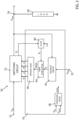
Figure 1 shows aswitching voltage regulator 1 comprising a four-switch non-inverting switching circuit, hereinafter referred to asswitching circuit 3, and acontrol device 5. - The
switching circuit 3 is formed by a first half-bridge 7, a second half-bridge 9 and aninductor 10. - The first half-
bridge 7 is formed by a first high-side switch 11 and a first low-side switch 13, here two N-MOS transistors, coupled in series between aninput terminal 15 and acommon node 17. - The
common node 17 is coupled to a reference potential line (ground) 18 through ashunt resistor 19. - An input voltage VIN is applied to the
input terminal 15 with respect toground 18. - The second half-
bridge 9 is formed by a second high-side switch 20 and by a second low-side switch 22, also here two N-MOS transistors, coupled in series between anoutput node 24 and thecommon node 17. - An output voltage VOUT, referred to
ground 18, is present at theoutput node 24 and is applied to a load 25. - The
inductor 10 is coupled between an intermediate node of the first half-bridge 7 and an intermediate node of the second half-bridge 9. - As a function of the ratio between the input voltage VIN and the output voltage VOUT, the
switching voltage regulator 1 may work in one of three operating modes also known as "buck" if VIN>VOUT, "boost" if VIN<VOUT and "buck-boost" if VIN≈VOUT. - Depending on the operating mode, by suitably controlling the switching of the first and the second half-
bridges - For this purpose, the
control device 5 is coupled to theinput node 15 and to theoutput node 24 and receives the reference voltage VREF. - Furthermore, it is known to design the
control device 5 so that the operation of theregulator 1 is current-controlled. - In this regard, the
control device 5 is coupled to theshunt resistor 19 and detects the shunt voltage VS which drops on theshunt resistor 19 and which is a function of the current flowing, in use, through theinductor 10. - The
control device 5, starting from the input voltage VIN, the output voltage VOUT, the reference voltage VREF and the shunt voltage VS, generates four switch control signals H1, L1, H2, L2, which control the switching respectively of the first high-side switch 11, the first low-side switch 13, the second high-side switch 20 and the second low-side switch 22. - In the buck, boost or buck-boost modes, the
switches regulator 1 alternates between an ON-phase, wherein the inductor current increases, and an OFF-phase, wherein the inductor current decreases. - The
control device 5 forms a closed-loop control circuit which modifies the switch control signals H1, L1, H2, L2 as a function of the shunt signal VS, so that the output voltage VOUT is kept equal to the reference voltage VREF. - In detail, the
control device 5 compares the shunt voltage VS with a threshold that is a function of a difference between the output voltage VOUT and the reference voltage VREF and, in response, modifies the duration of the ON- and OFF-phases. - However, the Applicant has observed that the known regulators are subject to a high noise in the shunt voltage VS. This noise modifies the behavior of the shunt voltage VS with respect to the expected behavior, compromising the correct functioning of the
control device 5. - In fact, the noise in the shunt voltage VS may be such as to alter the comparison between the shunt voltage VS and the aforementioned threshold. This may lead to the phenomenon of subharmonics generation in the current that flows, in use, through the
inductor 10, especially for high values of the inductor current. - Furthermore, the phenomenon of subharmonics in the inductor current may also cause the generation of audio and electromagnetic noise and long-term instability of the same regulator.
- According to one approach, the
control device 5 comprises a filter having a fixed time constant which filters the shunt voltage VS. However, this approach does not allow to solve the problems caused by the noise of the shunt voltage VS and the resulting generation of subharmonics in the inductor current. - The aim of the present invention is to overcome the disadvantages of the prior art.
- According to the present invention there are provided a control device for a switching voltage regulator, a switching voltage regulator and a control method for a switching voltage regulator, as defined in the appended claims.
- For a better understanding of the present invention, some embodiments thereof are now described, purely by way of nonlimiting example, with reference to the attached drawings, wherein:
-
figure 1 shows a circuit diagram of a switching voltage regulator; -
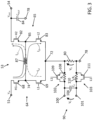
figure 2 shows a block diagram of a switching voltage regulator comprising a filter; -
figure 3 shows a detailed circuit diagram of a portion of the voltage regulator offigure 2 including the filter according to an embodiment; and -
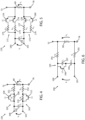
figures 4-8 show circuit diagrams of the filter offigure 2 according to different embodiments. -
Figure 2 shows a block diagram of aswitching voltage regulator 50, hereinafter also simply referred to asregulator 50, comprising aswitching circuit 53 and acontrol device 55, which are mutually coupled. - The
regulator 50 has aninput node 51 from which it receives an input voltage VIN, areference node 52 from which it receives a nominal or reference voltage VREF, and anoutput node 54 to which it provides an output voltage VOUT. A load 58 is coupled to theoutput node 54 of theregulator 50. - In detail, the
regulator 50 is a DC-DC converter of the buck-boost type, configured to generate the output voltage - VOUT, starting from the input voltage VIN, so that the output voltage VOUT is equal to the reference voltage VREF, which may be chosen by a user as a function of the specific application.
- The
switching circuit 53 and thecontrol device 55 may be integrated in a same die or formed in different dies. - The
switching circuit 53, shown in detail infigure 3 , is here a four-switch non-inverting circuit, in particular configured to operate in buck, boost or buck-boost (or transition) mode, depending on whether the input voltage VIN is respectively higher, lower than or approximately equal with respect to the output voltage VOUT (or to the reference voltage VREF). - In detail, the
switching circuit 53 is formed by a first half-bridge 64 and by a second half-bridge 65. - The first half-
bridge 64 is formed by a first high-side switch 68 and a first low-side switch 69, here two N-MOS transistors, coupled in series between theinput node 51 and acommon node 72. - In detail, the first high-
side switch 68 is coupled between theinput node 51 and anintermediate node 74 of the first half-bridge 64 and the first low-side switch 69 is coupled between theintermediate node 74 of the first half-bridge 64 and thecommon node 72. - The
input node 51 is at the input voltage VIN with respect to a reference potential line (ground) 78. - The
common node 72 is coupled toground 78 through a resistive element, here ashunt resistor 80, having resistance RS. - The second half-
bridge 65 is formed by a second high-side switch 82 and by a second low-side switch 83, also here two N-MOS transistors, coupled in series between theoutput node 54 and thecommon node 72. - In detail, the second high-
side switch 82 is coupled between theoutput node 54 and anintermediate node 85 of the second half-bridge 65 and the second low-side switch 83 is coupled between theintermediate node 85 of the second half-bridge 65 and thecommon node 72. - The
output node 54 provides the output voltage VOUT, with respect toground 78. - The
switching circuit 53 also comprises aninductor 87 having inductance L and coupled between theintermediate node 74 of the first half-bridge 64 and theintermediate node 85 of the second half-bridge 65. - The first high-
side switch 68, the first low-side switch 69, the second high-side switch 82, and the second low-side switch 83 are each controlled by a respective switch control signal H1, L1, H2, L2. - The
switching circuit 53 also comprises anoutput capacitor 84 having capacitance COUT, coupled between theoutput node 54 and theground 78. - The
control device 55 is configured to perform a current-control of theswitching circuit 53. - The
control device 55 is coupled to theoutput node 54 and thereference node 52. - Furthermore, the
control device 55 is coupled to theshunt resistor 80 so as to detect a measurement or shunt voltage VS indicative of the inductor current flowing, in use, through theshunt resistor 80. - With reference to
figure 2 , thecontrol device 55 comprises afilter 90, described in detail below, which receives the shunt voltage VS and generates a filtered signal, here a filtered voltage VF; and a loop control circuit, comprising afeedback circuit 92, aPWM modulator 94, and adriving logic circuit 96, which provides the switch control signals H1, L1, H2, L2 as a function of the filtered signal VF, so that the output voltage VOUT is kept equal to the reference voltage VREF. - In detail, the
feedback circuit 92 is coupled to theoutput node 54 and to thereference node 52 and generates a control signal, here a control voltage VC. - The
PWM modulator 94 receives the control voltage VC and the filtered voltage VF and provides in response a PWM modulated signal. - The
driving logic circuit 96 provides the switch control signals H1, L1, H2, L2 starting from the PWM modulated signal. - In the embodiment shown, the
control device 55 also comprises amode determination module 98 which receives the input voltage VIN and the output voltage VOUT and provides in response a mode signal MOD which indicates whether theregulator 50 is in the buck, boost or buck-boost operating mode. - For example, the
mode determination module 98 may compare the difference between the input voltage VIN and the output voltage VOUT with a first threshold Vth1 and a second threshold Vth2. - For example, if VIN < VOUT - Vth1 then the
regulator 50 is in boost mode. If VIN > VOUT + Vth2 then theregulator 50 is in buck mode. If VOUT - Vth1 < VIN < VOUT + Vth2 then theregulator 50 is in buck-boost or transition mode. - The
feedback circuit 92, thePWM modulator 94 and the drivinglogic circuit 96 may receive the mode signal MOD, such that the respective operation is a function of the operating mode of theregulator 50, in a per se known manner. - The
feedback circuit 92 detects an error signal indicative of a difference between the output voltage VOUT and the reference voltage VREF and provides in response the control voltage VC. - For example, the
feedback circuit 92 may comprise an error amplifier, such as an operational transconductance amplifier (OTA) which receives and amplifies the error signal, and a filtering network coupled to the output of the OTA. - According to an embodiment, the control voltage VC may be indicative of further current-control parameters, for example offset, slope, etc., of a per se known type, as a function of the specific control mode of the
regulator 50, for example peak or valley current-control. - The
PWM modulator 94 compares the filtered voltage VF, indicative of the current flowing in the switchingcircuit 53, with the control voltage VC, indicative of the difference between the output voltage VOUT and the reference voltage VREF, and provides in response the PWM modulated signal. - The PWM modulated signal has a fixed period and a duty-cycle which is variable at each cycle (or period) of the PWM modulated signal.
- In detail, in each cycle of the PWM modulated signal, the PWM modulated signal has a first semiperiod of duration TON and a second semiperiod of duration TOFF which define an ON-phase and, respectively, an OFF-phase of the
regulator 50. In the ON-phase, the current flowing through theinductor 87 has an increasing trend over time. In the OFF-phase, the current flowing through theinductor 87 has a decreasing trend over time. - The
PWM modulator 94 modifies, in use, the duty cycle of the PWM modulated signal as a function of the comparison between the filtered voltage VF and the control voltage VC. - The driving
logic circuit 96 provides, in a per se known manner, the switch control signals H1, L1, H2, L2 starting from the PWM modulated signal, as a function of the actual operating mode of theregulator 50. - In practice, the
feedback circuit 92, thePWM modulator 94 and the drivinglogic circuit 96 form a closed loop control circuit. - With reference to
figures 2 and3 , thefilter 90 receives a filter control signal which is indicative of the actual operating mode of theregulator 50; in particular here thefilter 90 receives the switch control signal L1 which controls the first low-side switch 69. - The
filter 90 is therefore a filter variable as a function of the actual operating mode of theregulator 50. - In detail, the
filter 90 is a low-pass filter having a time constant variable as a function of the actual operating mode of theregulator 50. - The
filter 90 comprises a first input node coupled to a terminal of theshunt resistor 80, here coinciding with thecommon node 72 and therefore indicated by the same reference number; a second input node coupled to a second terminal of theshunt resistor 80, here coinciding with theground 78 and therefore indicated by the same reference number; and a first and asecond output node - In this embodiment, the
filter 90 comprises a firstresistive element 102 coupled between thefirst input node 72 and thefirst output node 100 of thefilter 90; a secondresistive element 103 coupled between thesecond input node 78 and thesecond output node 101 of thefilter 90; and a capacitive element, here acapacitor 104, having a capacitance CF and coupled between the first and thesecond output nodes filter 90. - The capacitance CF may be chosen as a function of the specific application.
- The capacitance CF may be, for example, on the order of a few nF if the
capacitor 104 is of discrete type or of a few tens of pF if thecapacitor 104 is integrated in thecontrol device 55. - The first
resistive element 102 has a variable resistance as a function of the switch control signal L1. - The first
resistive element 102 is a parallel circuit comprising aresistor 108 having resistance RF and aswitch 109, here an NMOS transistor having an on-state resistance Rds,ON, lower than the resistance RF. - The resistances RF and Rds,ON may be chosen as a function of the specific application.
- For example, the resistance RF may be on the order of a few Ohms and the on-state resistance Rds,ON may be of a few fractions of an Ohm, if the
resistor 108 and theswitch 109 are of discrete type. - For example, the resistance RF may be on the order of a few kOhms, if the
resistor 108 is integrated into thecontrol device 55. - The use of higher values of the resistance RF and lower values of the capacitance CF in the case where the
capacitor 104 and theresistor 108 are integrated in thecontrol device 55, with respect to the case where thecapacitor 104 and theresistor 108 are discrete elements, allows to obtain a low die area occupancy of thefilter 90. - The second
resistive element 103 has a resistance variable as a function of the signal L1. - The second
resistive element 103 is a parallel circuit comprising aresistor 110 having resistance RF and aswitch 111, here an NMOS transistor, having an on-state resistance Rds,ON lower than the resistance RF. - The
switches - What has been described above for the
resistor 108 and theswitch 109 may also be applied to theresistor 110 and theswitch 111. - In particular, in this embodiment, the first and the second
resistive elements - In use, when the
regulator 50 is in the boost mode, the drivinglogic circuit 96 provides the switch control signal H1 so as to keep the first high-side switch 68 closed (i.e., so as to keep the correspondingtransistor 68 on, thus allowing a flow of current), and the switch control signal L1 so as to keep the first low-side switch 69 open (i.e., so as to keep the correspondingtransistor 69 off, thus blocking a flow of current). - At the same time, in the boost mode, the driving
logic circuit 96 provides the switch signals H2, L2 so as to control the alternating opening of the second high-side switch 82 and of the second low-side switch 83. - In detail, in each cycle of the PWM modulated signal, in the ON-phase of the boost mode, a current (indicated by a dotted arrow IL3 in
figure 3 ) may flow through the first high-side switch 68, theinductor 87, the second low-side switch 83 and theshunt resistor 80. In the OFF-phase, a current (indicated by a dashed arrow IL1 infigure 3 ) may flow through the first high-side switch 68, theinductor 87 and the second high-side switch 82. - In the boost mode, the switch control signal L1 keeps open, in addition to the first low-
side switch 69, also theswitches filter 90 both in the ON-phase and in the OFF-phase. - Consequently, the resistance of the first and the second
resistive elements resistors - The
filter 90 therefore has, in the boost mode, a time constant τbo which is a function of the resistance RF and the capacitance CF; in particular, in the embodiment shown, the time constant τbo is given by 2·CF·RF since thefilter 90 is a differential filter. - When the
regulator 50 is in the buck mode, the drivinglogic circuit 96 provides the switch control signal H2 so as to keep the second high-side switch 82 closed, and the switch control signal L2 so as to keep the second low-side switch 83 open. - The driving
logic circuit 96 provides the switch signals H1, L1 so as to control the alternating opening of the first high-side switch 68 and the first low-side switch 69. - In detail, in each cycle of the PWM modulated signal, in the ON-phase of the buck mode, a current (indicated by the dashed arrow IL1 in
figure 3 ) may flow through the first high-side switch 68, theinductor 87 and the second high-side switch 82. In the OFF-phase, a current (indicated by a dash-dot arrow IL2 infigure 3 ) may flow through the second high-side switch 82, theinductor 87, the first low-side switch 69 and theshunt resistor 80. - In practice, in the OFF-phase of the buck mode, when the inductor current IL2 flows through the
shunt resistor 80, the switch control signal L1 keeps theswitches filter 90 closed. - Consequently, the resistance of the first and the second
resistive elements switches - The resistance Rds,on is lower than the resistance RF.
- Consequently, in buck mode, the
filter 90 has a time constant τbu given by 2·CF·Rds,on, and therefore lower than the time constant τbo of the boost mode. - In the buck-boost or transition mode, the driving
logic circuit 96 controls the switches H1, L1, H2, L2 so as to alternate the current paths indicated infigure 3 by the arrows IL1, IL2, IL3, in a per se known manner. - In practice, the
control device 55 alternates a period of the PWM modulated signal wherein theregulator 50 is in the boost mode to a subsequent period of the PWM modulated signal wherein theregulator 50 is in the buck mode. - In practice, the
filter 90 is a filter, here of differential type, having a variable time constant which depends on the capacitance CF and on the resistance RF or Rds,on, as a function of the value of the switch control signal L1. - In addition to what has been discussed above for the values CF, RF and Rds,on, these may be chosen during the design step as a function of the specific values of the time constants τbo, τbu desired.
- For example, the values CF, RF and Rds,on may be chosen so that the time constants τbo, τbu are lower than a blanking time of the
regulator 50, wherein the blanking time is chosen as a function of the on and/or off transients of theswitches - The Applicant has observed that the possibility of automatically adjusting the time constant of the
filter 90 as a function of the actual operating mode of theregulator 50 allows to obtain optimal operation of theregulator 50 in any operating condition, for example independently of the input voltage VIN and of the load current flowing through theload 58. - In fact, the
filter 90 causes any noise in the shunt voltage VS to be suitably filtered in any operating mode of theregulator 50. In practice, thefilter 90 reduces the effects of this noise on the filtered voltage VF. - Since the loop control circuit formed by the
feedback circuit 92, thePWM modulator 94 and the drivinglogic circuit 96 generates the switching control signals H1, L1, H2, L2 as a function of the filtered signal VF, the noise of the shunt voltage VS does not affect the control of the switchingcircuit 53. - This allows to avoid, or in any case to reduce, the generation of subharmonics or other deviations of the inductor current.
- The
filter 90 therefore allows an improved operation of theregulator 50. - Furthermore, the possibility of modifying the time constant of the
filter 90 as a function the actual operating mode of theregulator 50 allows to compensate for any parasitic capacitances or inductances of theregulator 50. - In particular, the Applicant has observed that the fact that the
filter 90 may have, in the boost mode, a greater time constant than in the buck mode allows to adequately filter the noise in the shunt voltage VS and therefore to reduce and/or eliminate the generation of subharmonics in the inductor current both in boost mode and in the buck mode, even in the presence of high values, for example even higher than 20 A, of the load current. - In fact, the Applicant has observed that the inductor current may reach, in the boost mode, higher values than in the buck mode, for example if compared in case of
equal load 58. - High values of the inductor current accentuate the effects of any parasitic capacitances and/or inductances of the switching
circuit 53, for example formed by theshunt resistor 80 and/or by the current paths between theswitches ground 78. Consequently, the shunt voltage VS may be subject to higher noise values in boost mode than in the buck mode. - A high time constant in boost mode allows to filter out this greater noise.
- At the same time, the Applicant has verified that this high time constant may compromise the operation of the
regulator 50 in buck mode. - Consequently, the use of the
filter 90 having a greater time constant in boost mode than in the buck mode allows both to filter the noise of the shunt voltage VS and to ensure correct operation of theregulator 50 in both boost and buck modes, also in the presence of high inductor currents. -
Figure 4 shows a different embodiment of the filter, here indicated by 150, coupled to theshunt resistor 80 and providing the filtered voltage VF. Thefilter 150 has a general structure similar to that of thefilter 90 offigure 3 ; consequently, elements in common are indicated by the same reference numbers and are not further described. - The
filter 150 comprises, in addition to what has been described for thefilter 90, also a third and a fourthresistive element - The third
resistive element 151, here a resistor of resistance RF2, is arranged in series with the firstresistive element 102, here between theresistor 108 and thefirst input node 72 of thefilter 150. - The fourth
resistive element 152, here a resistor of resistance RF2, is arranged in series with the secondresistive element 103, here between theresistor 110 and thesecond input node 78 of thefilter 150. - In practice, in this embodiment, when the switch control signal L1 keeps the
switches filter 150 is given by RF+RF2. - When the switch control signal L1 keeps the
switches filter 150 is given by Rds,ON+RF2. - Consequently, also in this embodiment, the time constant of the
filter 150 depends on the actual operating mode of theregulator 50 and is greater in boost mode than in the buck mode. - In this embodiment, the resistance of the
filter 150 may be determined by theresistors switches filter 150 may be independent of any variations in the on-state resistance RDS,on of theswitches -
Figure 5 shows a different embodiment of the filter, here indicated by 170, coupled to theshunt resistor 80 and providing the filtered voltage VF. Thefilter 170 has a general structure similar to that of thefilter 90 offigure 3 ; consequently, elements in common are indicated by the same reference numbers and are not further described. - The
filter 170 here again comprises a first and a second resistive element, here indicated by 171 and 172, and thecapacitive element 104. - The first
resistive element 171 is a parallel circuit having a first branch formed by a series circuit comprising aresistor 173 of resistance RF1 and a switch, here anNMOS transistor 174; and a second branch formed by a series circuit comprising aresistor 175 of resistance RF2, and a switch, here anNMOS transistor 176. - The
switch 174 is controlled by the switch control signal L1. Theswitch 176 is controlled by the switch control signal L2. - The second
resistive element 172 is a parallel circuit having a first branch formed by a series circuit comprising aresistor 177 of resistance RF1 and a switch, here anNMOS transistor 178; and a second branch formed by a series circuit comprising aresistor 179 of resistance RF2, and a switch, here anNMOS transistor 180. - The
switch 178 is controlled by the switch control signal L1. Theswitch 180 is controlled by the switch control signal L2. - In this embodiment, the resistance RF2 is greater than the resistance RF1.
- Consequently, in the buck mode, when the
switches switches filter 170 is given by CF·(RF1+Rds,ON). - In the boost mode, when the
switches switches filter 170 is given by CF·(RF2+Rds,ON). - Since the resistance RF2 is greater than resistance RF1, the
filter 170 may have a greater time constant in the boost mode than in the buck mode. -
Figure 6 shows a further embodiment of the filter, here indicated by 190, coupled to theshunt resistor 80 and providing the filtered voltage VF. - In the
filter 190, the first and the second resistive elements are each formed by arespective resistor - The capacitive element, here indicated by 195, is a series circuit coupled between the first and the
second output nodes filter 190 and comprising thecapacitor 104 and a parallel circuit formed by aswitch 196, here an NMOS transistor, and acapacitor 197, here having capacitance CF. - The
switch 196 is controlled by the switch control signal L2 that controls the second low-side switch 83. - In the buck mode, the switch control signal L2 keeps the second low-
side switch 83 open. Consequently, the capacitance of thecapacitive element 195 is given by the series ofcapacitors - In the boost mode, particularly in the ON-phase wherein the inductor current flows in the
shunt resistor 80, the switch control signal L2 keeps the second low-side switch 83 closed (current IL3 infigure 3 ). Consequently, theswitch 196 is also closed. The capacitance of thecapacitive element 195 is therefore given by thecapacitor 104. - In practice, even in this embodiment, the time constant of the
filter 190 may be greater in the boost mode than in the buck mode. - Finally, it is clear that modifications and variations may be made to the
regulator 50 described and illustrated herein without thereby departing from the scope of the present invention, as defined in the attached claims. - The filter coupled to the
shunt resistor 80 may have a circuit diagram different from what has been described with reference tofigures 3-6 . - For example, the filter may be a common mode filter.
- For example, with reference to
figure 6 , the capacitive element may be a parallel circuit comprising a first branch having a fixed capacitor and a second branch having a series circuit comprising a switch and a fixed capacitor. In this case, the switch may be controlled by the switch control signal L1. - The filter may be of a different type, for example a bandpass filter wherein the time constants which determine the pass-band of the same filter are variable as a function of the actual operating mode of the
regulator 50. - For example, as shown in
figure 7 , the filter, here indicated by 200, may receive all the switch control signals H1, L1, H2, L2 and have a circuit diagram such as to make the time constant variable as a function of all the signals H1, L1, H2, L2, in particular such that the time constant of thefilter 200 is greater in the boost mode than in the buck mode. - For example, as shown in
figure 8 , the filter, here indicated by 210, may be controlled by the mode signal MOD generated by themode determination module 98 offigure 1 . In detail, the time constant of thefilter 200 is a function of the mode signal MOD, in particular such that the time constant of thefilter 200 is greater in the boost mode than in the buck mode. - Alternatively, the filter may be controlled by another signal internal to the
control device 55, for example generated by a specific circuit, indicative of the actual operating mode of theregulator 50. - For example, the
shunt resistor 80 may be a resistive element different from a discrete resistor, for example it may be obtained starting from an integrated resistance. - For example, the
shunt resistor 80 may be arranged in a different position in the switchingcircuit 53 with respect to what has been shown infigure 3 , either in the high side or in the low side of the switchingcircuit 53, such as in series with theinductor 87 between theintermediate nodes side switch 82 and theoutput node 54. In this manner, thecontrol device 55 may be configured to perform a current-control that is different from the valley-type one in buck mode and the peak-type one in boost mode. For example, if theshunt resistor 80 is arranged in the high side of the switchingcircuit 53, for example between the second high-side switch 82 and theoutput node 54, thecontrol device 55 may perform a valley-type current-control in boost mode and a peak-type current-control in buck mode. - For example, the
filters switching circuit 53 is formed, or by circuit elements integrated in the same die wherein thecontrol device 55 is formed. - The
filter feedback circuit 92, thePWM modulator 94 and thecontrol logic circuit 96 may be modules that are implemented as analog, digital or mixed-signal circuits, according to the specific application. - The switching circuit of the present regulator may be of a type other than what shown and described above; for example, it may be a switching circuit of the inverting or non-inverting type and having a number of drivable switches other than four.
- In general, as it emerges from what described above, the filter, which is variable as a function of the actual operating mode of the converter, may be used in various DC-DC converters having a shunt current measurement chain.
- The embodiments described and illustrated above may be combined to form further solutions.
Claims (15)
- A control device (55) for a switching voltage regulator (50) of the buck-boost type comprising a switching circuit (53), the control device being configured to perform a current-control of the switching circuit, wherein the control device comprises:a filter (90; 150; 170; 200; 210) configured to be coupled to a resistive element (80) of the switching circuit and to provide a filtered signal (VF) starting from a measurement signal (VS) indicative of a current (IL2, IL3) flowing through the resistive element; anda loop control circuit (92, 94, 96) configured to generate one or more switching control signals (PWM, H1, L1, H2, L2) to drive the switching circuit, as a function of the filtered signal (VF),wherein the filter is configured to receive a filter control signal (L1; L1, L2; MOD) indicative of an actual operating mode of the switching voltage regulator, the filter being variable as a function of the filter control signal.
- The control device according to the preceding claim, wherein the filter (90; 150; 170; 200; 210) has a time constant that is variable as a function of the filter control signal.
- The control device according to claim 1 or 2, wherein the filter is a low-pass filter.
- The control device according to any of the preceding claims, wherein the filter is configured to have a first time constant (τbu) when the switching voltage regulator is in the buck operating mode and a second time constant (τbo) when the switching voltage regulator is in the boost operating mode, the second time constant being greater than the first time constant.
- The control device according to any of the preceding claims, wherein the filter control signal is one of the switching control signals (L1; L2).
- The control device according to any of the preceding claims, wherein the filter (90; 150; 170) comprises at least one resistive element (102, 103; 171, 172) having a resistance variable as a function of the filter control signal.
- The control device according to the preceding claim, wherein the resistive element comprises a parallel circuit including a resistor (108, 110) and a switch (109, 111), the switch being controlled by the filter control signal.
- The control device according to claim 6 or 7, wherein the filter control signal is a first filter control signal (L1), the filter (170) being configured to further receive a second filter control signal (L2) indicative of the actual operating mode of the voltage regulator and different from the first filter control signal, the resistive element (171, 172) of the filter comprising a parallel circuit having a first and a second branch each comprising a respective resistor (173, 175) and a respective switch (174, 176) connected to each other in series, the switch (174) of the first branch being controlled by the first filter control signal and the switch (176) of the second branch being controlled by the second filter control signal.
- The control device according to any of the preceding claims, wherein the filter (190) comprises at least one capacitive element (195) having a capacitance variable as a function of the filter control signal (L2).
- The control device according to any of the preceding claims, configured to perform a peak-type current-control when the switching voltage regulator is in boost mode and to perform a valley-type current-control when the switching voltage regulator is in buck mode.
- The control device according to any of the preceding claims, wherein the loop control circuit comprises a feedback circuit (92) configured to generate a control signal (VC) as a function of a difference between an output voltage (VOUT) and a reference voltage (VREF); a PWM modulator (94) configured to receive the filtered signal (VF) and the control signal (VC) and, in response, generate a modulated signal (PWM); and a driving logic circuit (96) configured to provide the switching control signals (H1, L1, H2, L2) as a function of the modulated signal.
- The control device according to any of the preceding claims, for a switching voltage regulator of the buck-boost type, wherein the switching circuit is of the non-inverting type and/or comprises at least four switches drivable by the one or more switching control signals.
- A switching voltage regulator (50) of the buck-boost type comprising the control device according to any of the preceding claims and the switching circuit (53), the switching circuit including a first half-bridge (64), a second half-bridge (65) and an inductor (87), the first half-bridge comprising a first and a second switch (68, 69) coupled in series between an input node (51) and a common reference potential node (72, 78), the second half-bridge including a third and a fourth switch (82, 83) coupled in series between an output node (54) and the common reference potential node, the inductor being coupled between intermediate nodes (74, 85) of the first and the second half-bridges, the switching circuit further comprising a resistive element (80), the filter (90; 150; 170; 200; 210) being coupled to the resistive element, wherein the first, the second, the third and the fourth switches are controlled respectively by a first, a second, a third and a fourth switching control signals (H1, L1, H2, L2) generated by the loop control circuit (92, 94, 96).
- The switching voltage regulator according to the preceding claim, wherein the filter (90; 150; 170; 200; 210) comprises electrical elements integrated in the control device (55) or discrete electrical elements.
- A control method for a switching voltage regulator (50) of the buck-boost type comprising a switching circuit (53) and a control device (55) configured to perform a current-control of the switching circuit, the control method comprising:filtering, by a filter (90; 150; 170; 200; 210) of the control device, a measurement signal (VS) indicative of a current (IL2, IL3) that flows through a resistive element (80) of the switching circuit, thereby generating in response a filtered signal (VF); andgenerating, by a loop control circuit (92, 94, 96) of the control device, one or more switching control signals (PWM, H1, L1, H2, L2) to drive the switching circuit, as a function of the filtered signal (VF),wherein the measurement signal is filtered as a function of an actual operating mode of the voltage regulator.
Applications Claiming Priority (1)
| Application Number | Priority Date | Filing Date | Title |
|---|---|---|---|
| IT102022000026799A IT202200026799A1 (en) | 2022-12-23 | 2022-12-23 | CONTROL DEVICE FOR A SWITCHING VOLTAGE REGULATOR HAVING IMPROVED CURRENT SENSING AND SWITCHING VOLTAGE REGULATOR |
Publications (1)
| Publication Number | Publication Date |
|---|---|
| EP4391335A1 true EP4391335A1 (en) | 2024-06-26 |
Family
ID=85461856
Family Applications (1)
| Application Number | Title | Priority Date | Filing Date |
|---|---|---|---|
| EP23215475.7A Withdrawn EP4391335A1 (en) | 2022-12-23 | 2023-12-11 | Control device for a switching voltage regulator having improved current detection and switching voltage regulator |
Country Status (3)
| Country | Link |
|---|---|
| US (1) | US20240210978A1 (en) |
| EP (1) | EP4391335A1 (en) |
| IT (1) | IT202200026799A1 (en) |
Families Citing this family (2)
| Publication number | Priority date | Publication date | Assignee | Title |
|---|---|---|---|---|
| IT202200008930A1 (en) * | 2022-05-03 | 2023-11-03 | St Microelectronics Srl | CONTROL DEVICE FOR A SWITCHING VOLTAGE REGULATOR AND SWITCHING VOLTAGE REGULATOR |
| IT202200013240A1 (en) * | 2022-06-22 | 2023-12-22 | St Microelectronics Srl | CONTROL DEVICE FOR A SWITCHING VOLTAGE REGULATOR WITH IMPROVED CONTROL PERFORMANCE AND CONTROL METHOD |
Citations (3)
| Publication number | Priority date | Publication date | Assignee | Title |
|---|---|---|---|---|
| US20120133347A1 (en) * | 2010-11-30 | 2012-05-31 | Microchip Technology Incorporated | Efficiency-optimizing, calibrated sensorless power/energy conversion in a switch-mode power supply |
| US20150381039A1 (en) * | 2014-06-26 | 2015-12-31 | Texas Instruments Incorporated | Cascaded buck boost dc to dc converter and controller for smooth transition between buck mode and boost mode |
| US20180219476A1 (en) * | 2017-01-31 | 2018-08-02 | Infineon Technologies Ag | Switched-capacitor circuit and method of operating a switched-capacitor circuit |
Family Cites Families (4)
| Publication number | Priority date | Publication date | Assignee | Title |
|---|---|---|---|---|
| JP6780596B2 (en) * | 2017-07-18 | 2020-11-04 | トヨタ自動車株式会社 | Switching circuit |
| US10707760B2 (en) * | 2017-10-30 | 2020-07-07 | Renesas Electronics America Inc. | Asynchronous controller for low power hysteretic buck-boost DC-DC controller |
| US10348185B1 (en) * | 2018-07-24 | 2019-07-09 | Infineon Technologies Ag | Output current sensing for DC/DC converter with external power stage |
| US12040706B2 (en) * | 2021-06-22 | 2024-07-16 | Texas Instruments Incorporated | Inductor property identification for power converters |
-
2022
- 2022-12-23 IT IT102022000026799A patent/IT202200026799A1/en unknown
-
2023
- 2023-12-11 EP EP23215475.7A patent/EP4391335A1/en not_active Withdrawn
- 2023-12-20 US US18/390,441 patent/US20240210978A1/en active Pending
Patent Citations (3)
| Publication number | Priority date | Publication date | Assignee | Title |
|---|---|---|---|---|
| US20120133347A1 (en) * | 2010-11-30 | 2012-05-31 | Microchip Technology Incorporated | Efficiency-optimizing, calibrated sensorless power/energy conversion in a switch-mode power supply |
| US20150381039A1 (en) * | 2014-06-26 | 2015-12-31 | Texas Instruments Incorporated | Cascaded buck boost dc to dc converter and controller for smooth transition between buck mode and boost mode |
| US20180219476A1 (en) * | 2017-01-31 | 2018-08-02 | Infineon Technologies Ag | Switched-capacitor circuit and method of operating a switched-capacitor circuit |
Also Published As
| Publication number | Publication date |
|---|---|
| IT202200026799A1 (en) | 2024-06-23 |
| US20240210978A1 (en) | 2024-06-27 |
Similar Documents
| Publication | Publication Date | Title |
|---|---|---|
| CN101753024B (en) | Pwm clock generation system and method to improve transient response of a voltage regulator | |
| US20240210978A1 (en) | Control device and method for a switching voltage regulator, and switching voltage regulator | |
| US11374483B2 (en) | DC-DC converter having a switch on-time control loop with a switched-capacitor circuit for error-based adjustment | |
| JP5054759B2 (en) | Method and apparatus for switching regulator control | |
| US8395368B2 (en) | Adaptive voltage position DC-DC regulators and the method thereof | |
| US8106640B2 (en) | Power supply control circuit, power supply device, power supply system, and method of controlling power supply control device | |
| US10826380B2 (en) | Switching converter, circuit and method for controlling the same | |
| US8044650B2 (en) | Methods and apparatus for current sensing in mutually coupled inductors | |
| US7274183B1 (en) | Versatile system for high-power switching controller in low-power semiconductor technology | |
| US20150370273A1 (en) | Hysteretic power converter with calibration circuit | |
| US20030214274A1 (en) | Multiple-phase power converter having current sharing and high frequency filtering | |
| US11626799B2 (en) | Converter circuit, corresponding device and method | |
| KR100881537B1 (en) | Droop Amplifier Circuits and Multiphase DC-DC Converters for DC-DC Regulators | |
| EP4297258B1 (en) | Control device for a switching voltage regulator having improved control performance and control method | |
| CN114389452A (en) | Switch converter and control circuit and control method thereof | |
| JP2024046438A (en) | Step-down DC/DC converter and its controller circuit | |
| EP4518120A1 (en) | Control device and method for switching voltage regulator | |
| US20250079993A1 (en) | Control device for a switching voltage regulator and control method | |
| CN118249621A (en) | Control apparatus and method for switching voltage regulator and switching voltage regulator | |
| US12388365B2 (en) | Auxiliary circuit of power converter and driving circuit | |
| US11848607B2 (en) | Simple constant current limit for SEPIC or boost converter | |
| TW202424678A (en) | Control circuit for adaptive noise margin control for a constant on time converter | |
| US20250062690A1 (en) | Apparatus comprising a controller for a switching converter | |
| US20250185133A1 (en) | Driver circuit for supplying a constant current to an led arrangement | |
| CN100403226C (en) | Droop amplifier circuit for DC-DC converter |
Legal Events
| Date | Code | Title | Description |
|---|---|---|---|
| PUAI | Public reference made under article 153(3) epc to a published international application that has entered the european phase |
Free format text: ORIGINAL CODE: 0009012 |
|
| STAA | Information on the status of an ep patent application or granted ep patent |
Free format text: STATUS: THE APPLICATION HAS BEEN PUBLISHED |
|
| AK | Designated contracting states |
Kind code of ref document: A1 Designated state(s): AL AT BE BG CH CY CZ DE DK EE ES FI FR GB GR HR HU IE IS IT LI LT LU LV MC ME MK MT NL NO PL PT RO RS SE SI SK SM TR |
|
| STAA | Information on the status of an ep patent application or granted ep patent |
Free format text: STATUS: REQUEST FOR EXAMINATION WAS MADE |
|
| 17P | Request for examination filed |
Effective date: 20241224 |
|
| STAA | Information on the status of an ep patent application or granted ep patent |
Free format text: STATUS: THE APPLICATION HAS BEEN WITHDRAWN |
|
| 18W | Application withdrawn |
Effective date: 20251128 |