EP4391130A1 - Power storage module - Google Patents
Power storage module Download PDFInfo
- Publication number
- EP4391130A1 EP4391130A1 EP23209834.3A EP23209834A EP4391130A1 EP 4391130 A1 EP4391130 A1 EP 4391130A1 EP 23209834 A EP23209834 A EP 23209834A EP 4391130 A1 EP4391130 A1 EP 4391130A1
- Authority
- EP
- European Patent Office
- Prior art keywords
- current collector
- positive
- negative
- electrode
- electrode side
- Prior art date
- Legal status (The legal status is an assumption and is not a legal conclusion. Google has not performed a legal analysis and makes no representation as to the accuracy of the status listed.)
- Pending
Links
Images
Classifications
-
- H—ELECTRICITY
- H01—ELECTRIC ELEMENTS
- H01M—PROCESSES OR MEANS, e.g. BATTERIES, FOR THE DIRECT CONVERSION OF CHEMICAL ENERGY INTO ELECTRICAL ENERGY
- H01M10/00—Secondary cells; Manufacture thereof
- H01M10/04—Construction or manufacture in general
- H01M10/0413—Large-sized flat cells or batteries for motive or stationary systems with plate-like electrodes
- H01M10/0418—Large-sized flat cells or batteries for motive or stationary systems with plate-like electrodes with bipolar electrodes
-
- H—ELECTRICITY
- H01—ELECTRIC ELEMENTS
- H01M—PROCESSES OR MEANS, e.g. BATTERIES, FOR THE DIRECT CONVERSION OF CHEMICAL ENERGY INTO ELECTRICAL ENERGY
- H01M10/00—Secondary cells; Manufacture thereof
- H01M10/04—Construction or manufacture in general
-
- H—ELECTRICITY
- H01—ELECTRIC ELEMENTS
- H01M—PROCESSES OR MEANS, e.g. BATTERIES, FOR THE DIRECT CONVERSION OF CHEMICAL ENERGY INTO ELECTRICAL ENERGY
- H01M10/00—Secondary cells; Manufacture thereof
- H01M10/05—Accumulators with non-aqueous electrolyte
- H01M10/058—Construction or manufacture
- H01M10/0585—Construction or manufacture of accumulators having only flat construction elements, i.e. flat positive electrodes, flat negative electrodes and flat separators
-
- H—ELECTRICITY
- H01—ELECTRIC ELEMENTS
- H01M—PROCESSES OR MEANS, e.g. BATTERIES, FOR THE DIRECT CONVERSION OF CHEMICAL ENERGY INTO ELECTRICAL ENERGY
- H01M10/00—Secondary cells; Manufacture thereof
- H01M10/42—Methods or arrangements for servicing or maintenance of secondary cells or secondary half-cells
-
- H—ELECTRICITY
- H01—ELECTRIC ELEMENTS
- H01M—PROCESSES OR MEANS, e.g. BATTERIES, FOR THE DIRECT CONVERSION OF CHEMICAL ENERGY INTO ELECTRICAL ENERGY
- H01M10/00—Secondary cells; Manufacture thereof
- H01M10/42—Methods or arrangements for servicing or maintenance of secondary cells or secondary half-cells
- H01M10/48—Accumulators combined with arrangements for measuring, testing or indicating the condition of cells, e.g. the level or density of the electrolyte
-
- H—ELECTRICITY
- H01—ELECTRIC ELEMENTS
- H01M—PROCESSES OR MEANS, e.g. BATTERIES, FOR THE DIRECT CONVERSION OF CHEMICAL ENERGY INTO ELECTRICAL ENERGY
- H01M50/00—Constructional details or processes of manufacture of the non-active parts of electrochemical cells other than fuel cells, e.g. hybrid cells
- H01M50/50—Current conducting connections for cells or batteries
-
- H—ELECTRICITY
- H01—ELECTRIC ELEMENTS
- H01M—PROCESSES OR MEANS, e.g. BATTERIES, FOR THE DIRECT CONVERSION OF CHEMICAL ENERGY INTO ELECTRICAL ENERGY
- H01M50/00—Constructional details or processes of manufacture of the non-active parts of electrochemical cells other than fuel cells, e.g. hybrid cells
- H01M50/50—Current conducting connections for cells or batteries
- H01M50/531—Electrode connections inside a battery casing
-
- H—ELECTRICITY
- H01—ELECTRIC ELEMENTS
- H01M—PROCESSES OR MEANS, e.g. BATTERIES, FOR THE DIRECT CONVERSION OF CHEMICAL ENERGY INTO ELECTRICAL ENERGY
- H01M50/00—Constructional details or processes of manufacture of the non-active parts of electrochemical cells other than fuel cells, e.g. hybrid cells
- H01M50/50—Current conducting connections for cells or batteries
- H01M50/543—Terminals
-
- H—ELECTRICITY
- H01—ELECTRIC ELEMENTS
- H01M—PROCESSES OR MEANS, e.g. BATTERIES, FOR THE DIRECT CONVERSION OF CHEMICAL ENERGY INTO ELECTRICAL ENERGY
- H01M50/00—Constructional details or processes of manufacture of the non-active parts of electrochemical cells other than fuel cells, e.g. hybrid cells
- H01M50/50—Current conducting connections for cells or batteries
- H01M50/569—Constructional details of current conducting connections for detecting conditions inside cells or batteries, e.g. details of voltage sensing terminals
-
- H—ELECTRICITY
- H01—ELECTRIC ELEMENTS
- H01M—PROCESSES OR MEANS, e.g. BATTERIES, FOR THE DIRECT CONVERSION OF CHEMICAL ENERGY INTO ELECTRICAL ENERGY
- H01M50/00—Constructional details or processes of manufacture of the non-active parts of electrochemical cells other than fuel cells, e.g. hybrid cells
- H01M50/50—Current conducting connections for cells or batteries
- H01M50/572—Means for preventing undesired use or discharge
- H01M50/584—Means for preventing undesired use or discharge for preventing incorrect connections inside or outside the batteries
- H01M50/586—Means for preventing undesired use or discharge for preventing incorrect connections inside or outside the batteries inside the batteries, e.g. incorrect connections of electrodes
-
- H—ELECTRICITY
- H01—ELECTRIC ELEMENTS
- H01M—PROCESSES OR MEANS, e.g. BATTERIES, FOR THE DIRECT CONVERSION OF CHEMICAL ENERGY INTO ELECTRICAL ENERGY
- H01M2200/00—Safety devices for primary or secondary batteries
-
- Y—GENERAL TAGGING OF NEW TECHNOLOGICAL DEVELOPMENTS; GENERAL TAGGING OF CROSS-SECTIONAL TECHNOLOGIES SPANNING OVER SEVERAL SECTIONS OF THE IPC; TECHNICAL SUBJECTS COVERED BY FORMER USPC CROSS-REFERENCE ART COLLECTIONS [XRACs] AND DIGESTS
- Y02—TECHNOLOGIES OR APPLICATIONS FOR MITIGATION OR ADAPTATION AGAINST CLIMATE CHANGE
- Y02E—REDUCTION OF GREENHOUSE GAS [GHG] EMISSIONS, RELATED TO ENERGY GENERATION, TRANSMISSION OR DISTRIBUTION
- Y02E60/00—Enabling technologies; Technologies with a potential or indirect contribution to GHG emissions mitigation
- Y02E60/10—Energy storage using batteries
-
- Y—GENERAL TAGGING OF NEW TECHNOLOGICAL DEVELOPMENTS; GENERAL TAGGING OF CROSS-SECTIONAL TECHNOLOGIES SPANNING OVER SEVERAL SECTIONS OF THE IPC; TECHNICAL SUBJECTS COVERED BY FORMER USPC CROSS-REFERENCE ART COLLECTIONS [XRACs] AND DIGESTS
- Y02—TECHNOLOGIES OR APPLICATIONS FOR MITIGATION OR ADAPTATION AGAINST CLIMATE CHANGE
- Y02P—CLIMATE CHANGE MITIGATION TECHNOLOGIES IN THE PRODUCTION OR PROCESSING OF GOODS
- Y02P70/00—Climate change mitigation technologies in the production process for final industrial or consumer products
- Y02P70/50—Manufacturing or production processes characterised by the final manufactured product
Definitions
- the present disclosure relates to a power storage module.
- Japanese Patent Laying-Open No. 2022-37493 discloses a power storage device that includes a plurality of power storage modules and a plurality of conductive plates. Each of the conductive plates is disposed between mutually adjacent power storage modules.
- each power storage module in order to detect a voltage of each power storage module, it can be considered to connect a voltage detection terminal to each conductive plate connected to an outermost layer of the power storage module.
- each conductive plate is a current path of the power storage module, a measurement accuracy of a voltage is decreased due to the influence of a voltage drop between the power storage module and the conductive plate.
- the objective of the present disclosure is to provide a power storage module capable of suppressing a decrease in a measurement accuracy of a voltage.
- a power storage module includes a plurality of mutually stacked bipolar electrodes, a positive terminal electrode disposed on one side of the plurality of bipolar electrodes in a stacking direction of the plurality of bipolar electrodes, a negative terminal electrode disposed on another side of the plurality of bipolar electrodes in the stacking direction, a positive electrode current collector plate disposed to be stacked on the positive terminal electrode so as to make contact via a positive electrode side conductive adhesive material or directly with a surface of the positive terminal electrode on an opposite side to a surface facing the bipolar electrodes in the stacking direction, and electrically connected to the positive terminal electrode, a negative electrode current collector plate disposed to be stacked on the negative terminal electrode so as to make contact via a negative electrode side conductive adhesive material or directly with a surface of the negative terminal electrode on an opposite side to a surface facing the bipolar electrodes in the stacking direction, and electrically connected to the negative terminal electrode, a positive electrode side short circuit member with one end thereof connected to the positive terminal electrode and another
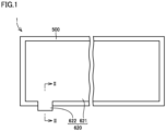
- Fig. 1 is a plan view schematically showing a power storage module in an embodiment of the present disclosure.
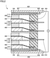
- Fig. 2 is a cross-sectional view taken along II-II line in Fig. 1 .
- a power storage module 1 includes a plurality of bipolar electrodes 100, a positive terminal electrode 200, a negative terminal electrode 300, a plurality of separators 400, a sealing portion 500, a positive electrode current collector plate 620, a negative electrode current collector plate 630, a positive electrode side conductive adhesive material 720, a negative electrode side conductive adhesive material 730, an inner voltage detection portion 810, a positive electrode side short circuit member 820, and a negative electrode side short circuit member 830.
- Each bipolar electrode 100 has a current collector 110, a positive electrode active material layer 120, and a negative electrode active material layer 130.
- Current collector 110 is made of metal, and is, for example, formed in a rectangular shape.
- Current collector 110 has a positive electrode current collector foil (illustration omitted) and a negative electrode current collector foil (illustration omitted).
- the positive electrode current collector foil is, for example, made of aluminum.
- the negative electrode current collector foil is, for example, made of copper foil.
- the negative electrode current collector foil is adhered to the positive electrode current collector foil by a conductive adhesive.
- Positive electrode active material layer 120 is provided on one surface in current collector 110, namely, on the surface of the positive electrode current collector foil.
- Negative electrode active material layer 130 is provided on the other surface in current collector 110, namely, on the surface of the negative electrode current collector foil.
- bipolar electrodes 100 are stacked such that positive electrode active material layer 120 in one of bipolar electrodes 100, and negative electrode active material layer 130 in bipolar electrode 100 adjacent to the one bipolar electrode 100, are facing each other.
- Positive terminal electrode 200 is disposed on one side (upper side in Fig. 2 ) of plurality of bipolar electrodes 100 in a stacking direction (vertical direction in Fig. 2 ).
- Positive terminal electrode 200 has a positive electrode current collector foil 112, and positive electrode active material layer 120 provided on positive electrode current collector foil 112.
- the configuration of positive electrode current collector foil 112 and positive electrode active material layer 120 in positive terminal electrode 200 is the same as the configuration of the positive electrode current collector foil and positive electrode active material layer 120 in bipolar electrode 100.
- Negative terminal electrode 300 is disposed on the other side (lower side in Fig. 2 ) of plurality of bipolar electrodes 100 in the stacking direction. Negative terminal electrode 300 has a negative electrode current collector foil 113, and negative electrode active material layer 130 provided on negative electrode current collector foil 113. The configuration of negative electrode current collector foil 113 and negative electrode active material layer 130 in negative terminal electrode 300 is the same as the configuration of the negative electrode current collector foil and negative electrode active material layer 130 in bipolar electrode 100.
- Each separator 400 is disposed between each electrode, more specifically, between positive electrode active material layer 120 and negative electrode active material layer 130. Each separator 400 insulates between each electrode. Each separator 400 is made of an insulating material, and allows the permeation of ions. A polyolefin microporous film or the like is provided as separator 400.
- Sealing portion 500 seals a region formed between each electrode. An electrolyte solution is filled in this region. Sealing portion 500 is made of an insulating material. Sealing portion 500 holds a peripheral edge portion of current collector 110 in each bipolar electrode 100, a peripheral edge portion of positive electrode current collector foil 112 in positive terminal electrode 200, a peripheral edge portion of negative electrode current collector foil 113 in negative terminal electrode 300, and a peripheral edge portion of each separator 400.
- Positive electrode current collector plate 620 is disposed outside (upper side in Fig. 2 ) positive terminal electrode 200 in the stacking direction. Positive electrode current collector plate 620 is disposed to be stacked on positive terminal electrode 200 so as to make contact via a positive electrode side conductive adhesive material 720 with a surface of positive terminal electrode 200 on an opposite side to a surface facing bipolar electrode 100 in the stacking direction. Positive electrode current collector plate 620 has a current collector plate body 621 and a positive electrode side voltage detection portion 622.
- Current collector plate body 621 is formed in a rectangular shape. As shown in Fig. 1 , the external shape of current collector plate body 621 in a plan view is one size smaller than the external shape of sealing portion 500 in a plan view. The external shape of current collector plate body 621 in a plan view is the same or larger than a region overlapping positive electrode active material layer 120 and negative electrode active material layer 130 in the stacking direction.
- Positive electrode side voltage detection portion 622 is a part where a voltmeter is connected. Positive electrode side voltage detection portion 622 has a shape that protrudes from current collector plate body 621 in a direction orthogonal to the stacking direction. As shown in Fig. 1 and Fig. 2 , positive electrode side voltage detection portion 622 has a shape that overhangs outward more than an end portion of sealing portion 500 in a direction orthogonal to the stacking direction.
- Positive electrode side conductive adhesive material 720 electrically connects positive terminal electrode 200 and positive electrode current collector plate 620. More specifically, positive electrode side conductive adhesive material 720 is provided between current collector plate body 621 and positive electrode current collector foil 112 in positive terminal electrode 200. Namely, positive electrode side voltage detection portion 622 is a part not overlapping positive electrode side conductive adhesive material 720 in the stacking direction. As shown in Fig. 2 , positive electrode side conductive adhesive material 720 is at least provided at a region, of the external surface of positive electrode current collector foil 112 of positive terminal electrode 200 in the stacking direction, overlapping positive electrode active material layer 120 and negative electrode active material layer 130 in the stacking direction, and is preferably provided on the entire region of a region exposed from sealing portion 500.
- Negative electrode current collector plate 630 is disposed outside (lower side in Fig. 2 ) negative terminal electrode 300 in the stacking direction. Negative electrode current collector plate 630 is disposed to be stacked on negative terminal electrode 300 so as to make contact via a negative electrode side conductive adhesive material 730 with a surface of negative terminal electrode 300 on an opposite side to a surface facing bipolar electrode 100 in the stacking direction. Negative electrode current collector plate 630 has a current collector plate body 631 and a negative electrode side voltage detection portion 632. Negative electrode side voltage detection portion 632 is a part where a voltmeter is connected. The structure of current collector plate body 631 and the structure of negative electrode side voltage detection portion 632 are substantially the same as the structure of current collector plate body 621 and the structure of positive electrode side voltage detection portion 622 in positive electrode current collector plate 620.
- Negative electrode side conductive adhesive material 730 electrically connects negative terminal electrode 300 and negative electrode current collector plate 630. More specifically, negative electrode side conductive adhesive material 730 is provided between current collector plate body 631 and negative electrode current collector foil 113 in negative terminal electrode 300. Namely, negative electrode side voltage detection portion 632 is a part not overlapping negative electrode side conductive adhesive material 730 in the stacking direction. As shown in Fig. 2 , negative electrode side conductive adhesive material 730 is at least provided at a region, of the external surface of negative electrode current collector foil 113 of negative terminal electrode 300 in the stacking direction, overlapping positive electrode active material layer 120 and negative electrode active material layer 130 in the stacking direction, and is preferably provided on the entire region of a region exposed from sealing portion 500.
- Inner voltage detection portion 810 is electrically connected to current collector 110 in each bipolar electrode 100. Inner voltage detection portion 810 is drawn out to the outside of sealing portion 500. Inner voltage detection portion 810 protrudes, for example, from sealing portion 500 in a direction orthogonal to the stacking direction. Note that, there may be current collector 110 to which inner voltage detection portion 810 is not connected. The end portion of each inner voltage detection portion 810 may be held by a connector (illustration omitted).
- Positive electrode side short circuit member 820 electrically connects positive terminal electrode 200 and positive electrode side voltage detection portion 622. More specifically, positive electrode side short circuit member 820 electrically connects positive electrode current collector foil 112 in positive terminal electrode 200 and positive electrode side voltage detection portion 622. Namely, one end of positive electrode side short circuit member 820 is connected to positive electrode current collector foil 112 in positive terminal electrode 200, and another end of positive electrode side short circuit member 820 is connected to positive electrode side voltage detection portion 622.
- each inner voltage detection portion 810 is held by the connector
- the other end of positive electrode side short circuit member 820 is not connected to positive electrode side voltage detection portion 622, and enlargement of the connector in the stacking direction is avoided, compared to the case where the other end of positive electrode side short circuit member 820 is also held by the connector.
- a connection portion (the one end of positive electrode side short circuit member 820) between positive electrode side short circuit member 820 and positive electrode current collector foil 112 in positive terminal electrode 200 is covered by sealing portion 500.
- An electrical resistance between positive terminal electrode 200 and current collector body 621 of positive electrode current collector plate 620 via positive electrode side conductive adhesive material 720 is smaller than an electrical resistance between positive terminal electrode 200 and voltage detection portion 622 via positive electrode side short circuit member 820.
- the material, cross-sectional area and the like of positive electrode side short circuit member 820 are set, so as to achieve a relationship of such electrical resistances.
- Negative electrode side short circuit member 830 electrically connects negative terminal electrode 300 and negative electrode side voltage detection portion 632. More specifically, negative electrode side short circuit member 830 electrically connects negative electrode current collector foil 113 in negative terminal electrode 300 and negative electrode side voltage detection portion 632. Namely, one end of negative electrode side short circuit member 830 is connected to negative electrode current collector foil 113 in negative terminal electrode 300, and another end of negative electrode side short circuit member 830 is connected to negative electrode side voltage detection portion 632. A connection portion (the one end of negative electrode side short circuit member 830) between negative electrode side short circuit member 830 and negative electrode current collector foil 113 in negative terminal electrode 300 is covered by sealing portion 500.
- An electrical resistance between negative terminal electrode 300 and current collector body 631 of negative electrode current collector plate 630 via negative electrode side conductive adhesive material 730 is smaller than an electrical resistance between negative terminal electrode 300 and voltage detection portion 632 via negative electrode side short circuit member 830.
- the material, cross-sectional area and the like of negative electrode side short circuit member 830 are set, so as to achieve a relationship of such electrical resistances.
- positive electrode side conductive adhesive material 720 and negative electrode side conductive adhesive material 730 may be omitted.
- positive electrode current collector foil 112 in positive terminal electrode 200 is connected directly to positive electrode current collector plate 620
- negative electrode current collector foil 113 in negative terminal electrode 300 is connected directly to negative electrode current collector plate 630.
- a power storage module including
- the power storage module described in Aspect 1 in which an electrical resistance between the positive terminal electrode and the positive electrode current collector plate in a contact region where the positive terminal electrode and the positive electrode current collector plate make contact via the positive electrode side conductive adhesive material or directly is lower than an electrical resistance between the positive terminal electrode and the positive electrode side voltage detection portion via the positive electrode side short circuit member, and an electrical resistance between the negative terminal electrode and the negative electrode current collector plate in a contact region where the negative terminal electrode and the negative electrode current collector plate make contact via the negative electrode side conductive adhesive material or directly is lower than an electrical resistance between the negative terminal electrode and the negative electrode side voltage detection portion via the negative electrode side short circuit member.
Landscapes
- Chemical & Material Sciences (AREA)
- Chemical Kinetics & Catalysis (AREA)
- Electrochemistry (AREA)
- General Chemical & Material Sciences (AREA)
- Engineering & Computer Science (AREA)
- Manufacturing & Machinery (AREA)
- Secondary Cells (AREA)
- Connection Of Batteries Or Terminals (AREA)
Abstract
Description
- This nonprovisional application is based on
Japanese Patent Application No. 2022-205797 filed on December 22, 2022 - The present disclosure relates to a power storage module.
-
Japanese Patent Laying-Open No. 2022-37493 - In the power storage device described in
Japanese Patent Laying-Open No. 2022-37493 - The objective of the present disclosure is to provide a power storage module capable of suppressing a decrease in a measurement accuracy of a voltage.
- A power storage module according to one aspect of the present disclosure includes a plurality of mutually stacked bipolar electrodes, a positive terminal electrode disposed on one side of the plurality of bipolar electrodes in a stacking direction of the plurality of bipolar electrodes, a negative terminal electrode disposed on another side of the plurality of bipolar electrodes in the stacking direction, a positive electrode current collector plate disposed to be stacked on the positive terminal electrode so as to make contact via a positive electrode side conductive adhesive material or directly with a surface of the positive terminal electrode on an opposite side to a surface facing the bipolar electrodes in the stacking direction, and electrically connected to the positive terminal electrode, a negative electrode current collector plate disposed to be stacked on the negative terminal electrode so as to make contact via a negative electrode side conductive adhesive material or directly with a surface of the negative terminal electrode on an opposite side to a surface facing the bipolar electrodes in the stacking direction, and electrically connected to the negative terminal electrode, a positive electrode side short circuit member with one end thereof connected to the positive terminal electrode and another end thereof connected to the positive electrode current collector plate, the positive electrode side short circuit member electrically connecting the positive terminal electrode and the positive electrode current collector plate, and a negative electrode side short circuit member with one end thereof connected to the negative terminal electrode and another end thereof connected to the negative electrode current collector plate, the negative electrode side short circuit member electrically connecting the negative terminal electrode and the negative electrode current collector plate, in which the positive electrode current collector plate has a positive electrode side voltage detection portion provided at a position not overlapping the positive terminal electrode in the stacking direction, the other end of the positive electrode side short circuit member is connected to the positive electrode side voltage detection portion, the negative electrode current collector plate has a negative electrode side voltage detection portion provided at a position not overlapping the negative terminal electrode in the stacking direction, and the other end of the negative electrode side short circuit member is connected to the negative terminal electrode and the negative electrode side voltage detection portion.
- The foregoing and other objects, features, aspects and advantages of the present disclosure will become more apparent from the following detailed description of the present disclosure when taken in conjunction with the accompanying drawings.
-
-
Fig. 1 is a plan view schematically showing a power storage module in an embodiment of the present disclosure. -
Fig. 2 is a cross-sectional view taken along II-II line inFig. 1 . -
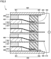
Fig. 3 is a cross-sectional view schematically showing a modified example of a power storage module. - An embodiment of the present disclosure will be described with reference to the figures. Note that, the same reference numerals are attached to same or corresponding members within the figures referred to hereinafter.
-
Fig. 1 is a plan view schematically showing a power storage module in an embodiment of the present disclosure.Fig. 2 is a cross-sectional view taken along II-II line inFig. 1 . As shown inFig. 1 andFig. 2 , apower storage module 1 includes a plurality ofbipolar electrodes 100, apositive terminal electrode 200, anegative terminal electrode 300, a plurality ofseparators 400, asealing portion 500, a positive electrodecurrent collector plate 620, a negative electrodecurrent collector plate 630, a positive electrode side conductiveadhesive material 720, a negative electrode side conductiveadhesive material 730, an innervoltage detection portion 810, a positive electrode sideshort circuit member 820, and a negative electrode sideshort circuit member 830. - Plurality of
bipolar electrodes 100 are mutually stacked. Eachbipolar electrode 100 has acurrent collector 110, a positive electrodeactive material layer 120, and a negative electrodeactive material layer 130. -
Current collector 110 is made of metal, and is, for example, formed in a rectangular shape.Current collector 110 has a positive electrode current collector foil (illustration omitted) and a negative electrode current collector foil (illustration omitted). The positive electrode current collector foil is, for example, made of aluminum. The negative electrode current collector foil is, for example, made of copper foil. The negative electrode current collector foil is adhered to the positive electrode current collector foil by a conductive adhesive. - Positive electrode
active material layer 120 is provided on one surface incurrent collector 110, namely, on the surface of the positive electrode current collector foil. Negative electrodeactive material layer 130 is provided on the other surface incurrent collector 110, namely, on the surface of the negative electrode current collector foil. - Plurality of
bipolar electrodes 100 are stacked such that positive electrodeactive material layer 120 in one ofbipolar electrodes 100, and negative electrodeactive material layer 130 inbipolar electrode 100 adjacent to the onebipolar electrode 100, are facing each other. -
Positive terminal electrode 200 is disposed on one side (upper side inFig. 2 ) of plurality ofbipolar electrodes 100 in a stacking direction (vertical direction inFig. 2 ).Positive terminal electrode 200 has a positive electrodecurrent collector foil 112, and positive electrodeactive material layer 120 provided on positive electrodecurrent collector foil 112. The configuration of positive electrodecurrent collector foil 112 and positive electrodeactive material layer 120 inpositive terminal electrode 200 is the same as the configuration of the positive electrode current collector foil and positive electrodeactive material layer 120 inbipolar electrode 100. - Negative
terminal electrode 300 is disposed on the other side (lower side inFig. 2 ) of plurality ofbipolar electrodes 100 in the stacking direction. Negativeterminal electrode 300 has a negative electrodecurrent collector foil 113, and negative electrodeactive material layer 130 provided on negative electrodecurrent collector foil 113. The configuration of negative electrodecurrent collector foil 113 and negative electrodeactive material layer 130 innegative terminal electrode 300 is the same as the configuration of the negative electrode current collector foil and negative electrodeactive material layer 130 inbipolar electrode 100. - Each
separator 400 is disposed between each electrode, more specifically, between positive electrodeactive material layer 120 and negative electrodeactive material layer 130. Eachseparator 400 insulates between each electrode. Eachseparator 400 is made of an insulating material, and allows the permeation of ions. A polyolefin microporous film or the like is provided asseparator 400. - Sealing
portion 500 seals a region formed between each electrode. An electrolyte solution is filled in this region.Sealing portion 500 is made of an insulating material.Sealing portion 500 holds a peripheral edge portion ofcurrent collector 110 in eachbipolar electrode 100, a peripheral edge portion of positive electrodecurrent collector foil 112 inpositive terminal electrode 200, a peripheral edge portion of negative electrodecurrent collector foil 113 innegative terminal electrode 300, and a peripheral edge portion of eachseparator 400. - Positive electrode
current collector plate 620 is disposed outside (upper side inFig. 2 )positive terminal electrode 200 in the stacking direction. Positive electrodecurrent collector plate 620 is disposed to be stacked onpositive terminal electrode 200 so as to make contact via a positive electrode side conductiveadhesive material 720 with a surface ofpositive terminal electrode 200 on an opposite side to a surface facingbipolar electrode 100 in the stacking direction. Positive electrodecurrent collector plate 620 has a currentcollector plate body 621 and a positive electrode sidevoltage detection portion 622. - Current
collector plate body 621 is formed in a rectangular shape. As shown inFig. 1 , the external shape of currentcollector plate body 621 in a plan view is one size smaller than the external shape of sealingportion 500 in a plan view. The external shape of currentcollector plate body 621 in a plan view is the same or larger than a region overlapping positive electrodeactive material layer 120 and negative electrodeactive material layer 130 in the stacking direction. - Positive electrode side
voltage detection portion 622 is a part where a voltmeter is connected. Positive electrode sidevoltage detection portion 622 has a shape that protrudes from currentcollector plate body 621 in a direction orthogonal to the stacking direction. As shown inFig. 1 andFig. 2 , positive electrode sidevoltage detection portion 622 has a shape that overhangs outward more than an end portion ofsealing portion 500 in a direction orthogonal to the stacking direction. - Positive electrode side conductive
adhesive material 720 electrically connectspositive terminal electrode 200 and positive electrodecurrent collector plate 620. More specifically, positive electrode side conductiveadhesive material 720 is provided between currentcollector plate body 621 and positive electrodecurrent collector foil 112 inpositive terminal electrode 200. Namely, positive electrode sidevoltage detection portion 622 is a part not overlapping positive electrode side conductiveadhesive material 720 in the stacking direction. As shown inFig. 2 , positive electrode side conductiveadhesive material 720 is at least provided at a region, of the external surface of positive electrodecurrent collector foil 112 ofpositive terminal electrode 200 in the stacking direction, overlapping positive electrodeactive material layer 120 and negative electrodeactive material layer 130 in the stacking direction, and is preferably provided on the entire region of a region exposed fromsealing portion 500. - Negative electrode
current collector plate 630 is disposed outside (lower side inFig. 2 )negative terminal electrode 300 in the stacking direction. Negative electrodecurrent collector plate 630 is disposed to be stacked onnegative terminal electrode 300 so as to make contact via a negative electrode side conductiveadhesive material 730 with a surface ofnegative terminal electrode 300 on an opposite side to a surface facingbipolar electrode 100 in the stacking direction. Negative electrodecurrent collector plate 630 has a currentcollector plate body 631 and a negative electrode sidevoltage detection portion 632. Negative electrode sidevoltage detection portion 632 is a part where a voltmeter is connected. The structure of currentcollector plate body 631 and the structure of negative electrode sidevoltage detection portion 632 are substantially the same as the structure of currentcollector plate body 621 and the structure of positive electrode sidevoltage detection portion 622 in positive electrodecurrent collector plate 620. - Negative electrode side conductive
adhesive material 730 electrically connects negativeterminal electrode 300 and negative electrodecurrent collector plate 630. More specifically, negative electrode side conductiveadhesive material 730 is provided between currentcollector plate body 631 and negative electrodecurrent collector foil 113 in negativeterminal electrode 300. Namely, negative electrode sidevoltage detection portion 632 is a part not overlapping negative electrode side conductiveadhesive material 730 in the stacking direction. As shown inFig. 2 , negative electrode side conductiveadhesive material 730 is at least provided at a region, of the external surface of negative electrodecurrent collector foil 113 of negativeterminal electrode 300 in the stacking direction, overlapping positive electrodeactive material layer 120 and negative electrodeactive material layer 130 in the stacking direction, and is preferably provided on the entire region of a region exposed from sealingportion 500. - Inner
voltage detection portion 810 is electrically connected tocurrent collector 110 in eachbipolar electrode 100. Innervoltage detection portion 810 is drawn out to the outside of sealingportion 500. Innervoltage detection portion 810 protrudes, for example, from sealingportion 500 in a direction orthogonal to the stacking direction. Note that, there may becurrent collector 110 to which innervoltage detection portion 810 is not connected. The end portion of each innervoltage detection portion 810 may be held by a connector (illustration omitted). - Positive electrode side
short circuit member 820 electrically connects positiveterminal electrode 200 and positive electrode sidevoltage detection portion 622. More specifically, positive electrode sideshort circuit member 820 electrically connects positive electrodecurrent collector foil 112 in positiveterminal electrode 200 and positive electrode sidevoltage detection portion 622. Namely, one end of positive electrode sideshort circuit member 820 is connected to positive electrodecurrent collector foil 112 in positiveterminal electrode 200, and another end of positive electrode sideshort circuit member 820 is connected to positive electrode sidevoltage detection portion 622. Accordingly, for example, in the case where an end portion of each innervoltage detection portion 810 is held by the connector, the other end of positive electrode sideshort circuit member 820 is not connected to positive electrode sidevoltage detection portion 622, and enlargement of the connector in the stacking direction is avoided, compared to the case where the other end of positive electrode sideshort circuit member 820 is also held by the connector. A connection portion (the one end of positive electrode side short circuit member 820) between positive electrode sideshort circuit member 820 and positive electrodecurrent collector foil 112 in positiveterminal electrode 200 is covered by sealingportion 500. An electrical resistance between positiveterminal electrode 200 andcurrent collector body 621 of positive electrodecurrent collector plate 620 via positive electrode side conductiveadhesive material 720 is smaller than an electrical resistance between positiveterminal electrode 200 andvoltage detection portion 622 via positive electrode sideshort circuit member 820. The material, cross-sectional area and the like of positive electrode sideshort circuit member 820 are set, so as to achieve a relationship of such electrical resistances. - Negative electrode side
short circuit member 830 electrically connects negativeterminal electrode 300 and negative electrode sidevoltage detection portion 632. More specifically, negative electrode sideshort circuit member 830 electrically connects negative electrodecurrent collector foil 113 in negativeterminal electrode 300 and negative electrode sidevoltage detection portion 632. Namely, one end of negative electrode sideshort circuit member 830 is connected to negative electrodecurrent collector foil 113 in negativeterminal electrode 300, and another end of negative electrode sideshort circuit member 830 is connected to negative electrode sidevoltage detection portion 632. A connection portion (the one end of negative electrode side short circuit member 830) between negative electrode sideshort circuit member 830 and negative electrodecurrent collector foil 113 in negativeterminal electrode 300 is covered by sealingportion 500. An electrical resistance between negativeterminal electrode 300 andcurrent collector body 631 of negative electrodecurrent collector plate 630 via negative electrode side conductiveadhesive material 730 is smaller than an electrical resistance between negativeterminal electrode 300 andvoltage detection portion 632 via negative electrode sideshort circuit member 830. The material, cross-sectional area and the like of negative electrode sideshort circuit member 830 are set, so as to achieve a relationship of such electrical resistances. - As described above, in
power storage module 1 in the present embodiment, since positive electrode sidevoltage detection portion 622 and positiveterminal electrode 200, which are electrically connected by positive electrode sideshort circuit member 820, become a same potential as each other, and negative electrode sidevoltage detection portion 632 and negativeterminal electrode 300, which are electrically connected by negative electrode sideshort circuit member 830, become a same potential as each other, a voltage ofpower storage module 1 can be measured, while suppressing a decrease in a measurement accuracy of a voltage, by measuring a voltage between positive electrode sidevoltage detection portion 622 and negative electrode sidevoltage detection portion 632. - In addition, for example, in the case where an abnormality (such as peeling of positive electrode side conductive adhesive material 720) occurs in a connection state between positive
terminal electrode 200 and positive electrodecurrent collector plate 620, since an electrical resistance between currentcollector plate body 621 and positiveterminal electrode 200 increases, a current flowing through positive electrode sideshort circuit member 820 increases rapidly. As a result of this, positive electrode sideshort circuit member 820 melts. Accordingly, it becomes possible to detect an abnormality of a connection state between positiveterminal electrode 200 and positive electrodecurrent collector plate 620, or a connection state between negativeterminal electrode 300 and negative electrodecurrent collector plate 630, by measuring a voltage between positive electrode sidevoltage detection portion 622 and negative electrode sidevoltage detection portion 632 in a state of providing positive electrode sideshort circuit member 820 and negative electrode sideshort circuit member 830. - In the above embodiment, as shown in
Fig. 3 , positive electrode side conductiveadhesive material 720 and negative electrode side conductiveadhesive material 730 may be omitted. In this case, positive electrodecurrent collector foil 112 in positiveterminal electrode 200 is connected directly to positive electrodecurrent collector plate 620, and negative electrodecurrent collector foil 113 in negativeterminal electrode 300 is connected directly to negative electrodecurrent collector plate 630. - The above-stated exemplified embodiments and examples are understood by a person skilled in the art, with the following specific aspects.
- A power storage module including
- a plurality of mutually stacked bipolar electrodes,
- a positive terminal electrode disposed on one side of the plurality of bipolar electrodes in a stacking direction of the plurality of bipolar electrodes,
- a negative terminal electrode disposed on another side of the plurality of bipolar electrodes in the stacking direction,
- a positive electrode current collector plate disposed to be stacked on the positive terminal electrode so as to make contact via a positive electrode side conductive adhesive material or directly with a surface of the positive terminal electrode on an opposite side to a surface facing the bipolar electrodes in the stacking direction, and electrically connected to the positive terminal electrode,
- a negative electrode current collector plate disposed to be stacked on the negative terminal electrode so as to make contact via a negative electrode side conductive adhesive material or directly with a surface of the negative terminal electrode on an opposite side to a surface facing the bipolar electrodes in the stacking direction, and electrically connected to the negative terminal electrode,
- a positive electrode side short circuit member with one end thereof connected to the positive terminal electrode and another end thereof connected to the positive electrode current collector plate, the positive electrode side short circuit member electrically connecting the positive terminal electrode and the positive electrode current collector plate, and
- a negative electrode side short circuit member with one end thereof connected to the negative terminal electrode and another end thereof connected to the negative electrode current collector plate, the negative electrode side short circuit member electrically connecting the negative terminal electrode and the negative electrode current collector plate, in which
- the positive electrode current collector plate has a positive electrode side voltage detection portion provided at a position not overlapping the positive terminal electrode in the stacking direction,
- the other end of the positive electrode side short circuit member is connected to the positive electrode side voltage detection portion,
- the negative electrode current collector plate has a negative electrode side voltage detection portion provided at a position not overlapping the negative terminal electrode in the stacking direction, and
- the other end of the negative electrode side short circuit member is connected to the negative terminal electrode and the negative electrode side voltage detection portion.
- In this power storage module, since the positive electrode side voltage detection portion and the positive terminal electrode, which are electrically connected by the positive electrode side short circuit member, become a same potential as each other, and the negative electrode side voltage detection portion and the negative terminal electrode, which are electrically connected by the negative electrode side short circuit member, become a same potential as each other, a decrease in a measurement accuracy of a voltage is suppressed, by measuring a voltage between the positive electrode side voltage detection portion and the negative electrode side voltage detection portion.
- In addition, for example, in the case where an abnormality (such as peeling of the positive electrode side conductive adhesive material) occurs in a connection state between the positive terminal electrode and the positive electrode current collector plate, since an electrical resistance between the positive electrode current collector plate and the positive terminal electrode increases, a current flowing through the positive electrode side short circuit member increases rapidly. Accordingly, it becomes possible to detect an abnormality of a connection state between the positive terminal electrode and the positive electrode current collector plate, or a connection state between the negative terminal electrode and the negative electrode current collector plate, by measuring a voltage between the positive electrode side voltage detection portion and the negative electrode side voltage detection portion.
- The power storage module described in
Aspect 1, in which an electrical resistance between the positive terminal electrode and the positive electrode current collector plate in a contact region where the positive terminal electrode and the positive electrode current collector plate make contact via the positive electrode side conductive adhesive material or directly is lower than an electrical resistance between the positive terminal electrode and the positive electrode side voltage detection portion via the positive electrode side short circuit member, and
an electrical resistance between the negative terminal electrode and the negative electrode current collector plate in a contact region where the negative terminal electrode and the negative electrode current collector plate make contact via the negative electrode side conductive adhesive material or directly is lower than an electrical resistance between the negative terminal electrode and the negative electrode side voltage detection portion via the negative electrode side short circuit member. - In this aspect, since a current flowing through the positive electrode side short circuit member and the negative electrode side short circuit member is reduced, a decrease in a measurement accuracy of a voltage between the positive electrode side voltage detection portion and the negative electrode side voltage detection portion is more surely suppressed.
- Although the embodiments of the present disclosure have been described, the embodiments disclosed this time should be considered as illustrative in all aspects and not limiting. The scope of the present disclosure is indicated by the claims and it is intended that all changes within the meaning and the scope equivalent to the claims are included.
Claims (2)
- A power storage module (1), comprising:a plurality of mutually stacked bipolar electrodes (100);a positive terminal electrode (200) disposed on one side of the plurality of bipolar electrodes in a stacking direction of the plurality of bipolar electrodes;a negative terminal electrode (300) disposed on another side of the plurality of bipolar electrodes in the stacking direction;a positive electrode current collector plate (620) disposed to be stacked on the positive terminal electrode so as to make contact via a positive electrode side conductive adhesive material (720) or directly with a surface of the positive terminal electrode on an opposite side to a surface facing the bipolar electrodes in the stacking direction, and electrically connected to the positive terminal electrode;a negative electrode current collector plate (630) disposed to be stacked on the negative terminal electrode so as to make contact via a negative electrode side conductive adhesive material (730) or directly with a surface of the negative terminal electrode on an opposite side to a surface facing the bipolar electrodes in the stacking direction, and electrically connected to the negative terminal electrode;a positive electrode side short circuit member (820) with one end thereof connected to the positive terminal electrode and another end thereof connected to the positive electrode current collector plate, the positive electrode side short circuit member (820) electrically connecting the positive terminal electrode and the positive electrode current collector plate; anda negative electrode side short circuit member (830) with one end thereof connected to the negative terminal electrode and another end thereof connected to the negative electrode current collector plate, the negative electrode side short circuit member (830) electrically connecting the negative terminal electrode and the negative electrode current collector plate, whereinthe positive electrode current collector plate has a positive electrode side voltage detection portion (622) provided at a position not overlapping the positive terminal electrode in the stacking direction,the other end of the positive electrode side short circuit member is connected to the positive electrode side voltage detection portion,the negative electrode current collector plate has a negative electrode side voltage detection portion (632) provided at a position not overlapping the negative terminal electrode in the stacking direction, andthe other end of the negative electrode side short circuit member is connected to the negative terminal electrode and the negative electrode side voltage detection portion.
- The power storage module according to claim 1, whereinan electrical resistance between the positive terminal electrode (200) and the positive electrode current collector plate (620) in a contact region where the positive terminal electrode and the positive electrode current collector plate make contact via the positive electrode side conductive adhesive material (720) or directly is lower than an electrical resistance between the positive terminal electrode and the positive electrode side voltage detection portion via the positive electrode side short circuit member (820), andan electrical resistance between the negative terminal electrode (300) and the negative electrode current collector plate (630) in a contact region where the negative terminal electrode and the negative electrode current collector plate make contact via the negative electrode side conductive adhesive material (730) or directly is lower than an electrical resistance between the negative terminal electrode and the negative electrode side voltage detection portion via the negative electrode side short circuit member.
Applications Claiming Priority (1)
| Application Number | Priority Date | Filing Date | Title |
|---|---|---|---|
| JP2022205797A JP2024090122A (en) | 2022-12-22 | 2022-12-22 | Energy Storage Module |
Publications (1)
| Publication Number | Publication Date |
|---|---|
| EP4391130A1 true EP4391130A1 (en) | 2024-06-26 |
Family
ID=88833618
Family Applications (1)
| Application Number | Title | Priority Date | Filing Date |
|---|---|---|---|
| EP23209834.3A Pending EP4391130A1 (en) | 2022-12-22 | 2023-11-14 | Power storage module |
Country Status (5)
| Country | Link |
|---|---|
| US (1) | US20240213514A1 (en) |
| EP (1) | EP4391130A1 (en) |
| JP (1) | JP2024090122A (en) |
| KR (1) | KR102931542B1 (en) |
| CN (1) | CN118249052A (en) |
Families Citing this family (1)
| Publication number | Priority date | Publication date | Assignee | Title |
|---|---|---|---|---|
| JP2026507825A (en) | 2023-07-31 | 2026-03-06 | エルジー・ケム・リミテッド | Carbon nanotube dispersion and its manufacturing method |
Citations (3)
| Publication number | Priority date | Publication date | Assignee | Title |
|---|---|---|---|---|
| US20200028145A1 (en) * | 2017-03-03 | 2020-01-23 | Nissan Motor Co., Ltd. | Secondary battery and secondary battery control method |
| JP2022003627A (en) * | 2020-06-23 | 2022-01-11 | 株式会社豊田自動織機 | Power storage module |
| JP2022037493A (en) | 2020-08-25 | 2022-03-09 | 株式会社豊田自動織機 | Power storage device |
-
2022
- 2022-12-22 JP JP2022205797A patent/JP2024090122A/en active Pending
-
2023
- 2023-11-14 EP EP23209834.3A patent/EP4391130A1/en active Pending
- 2023-12-06 US US18/530,839 patent/US20240213514A1/en active Pending
- 2023-12-08 CN CN202311677900.5A patent/CN118249052A/en active Pending
- 2023-12-15 KR KR1020230182748A patent/KR102931542B1/en active Active
Patent Citations (3)
| Publication number | Priority date | Publication date | Assignee | Title |
|---|---|---|---|---|
| US20200028145A1 (en) * | 2017-03-03 | 2020-01-23 | Nissan Motor Co., Ltd. | Secondary battery and secondary battery control method |
| JP2022003627A (en) * | 2020-06-23 | 2022-01-11 | 株式会社豊田自動織機 | Power storage module |
| JP2022037493A (en) | 2020-08-25 | 2022-03-09 | 株式会社豊田自動織機 | Power storage device |
Also Published As
| Publication number | Publication date |
|---|---|
| KR20240100254A (en) | 2024-07-01 |
| CN118249052A (en) | 2024-06-25 |
| US20240213514A1 (en) | 2024-06-27 |
| KR102931542B1 (en) | 2026-02-27 |
| JP2024090122A (en) | 2024-07-04 |
Similar Documents
| Publication | Publication Date | Title |
|---|---|---|
| US11811095B2 (en) | Battery pack including busbar assembly having flexible substrate and insulating film | |
| US10916796B1 (en) | Selective charging matrix for rechargeable batteries | |
| KR20200080076A (en) | A battery module having a structure capable of accurate temperature sensing, a battery pack and a vehicle comprising the same | |
| KR20200080077A (en) | A battery module having a structure with an improved energy density, a battery pack and a vehicle comprising the same | |
| US20190181394A1 (en) | Prismatic secondary battery and method for manufacturing same | |
| JP2004014516A (en) | Battery equipped with housing | |
| US20110281151A1 (en) | Battery pack | |
| EP3483980B1 (en) | Battery module having simple sensing structure | |
| KR20230092218A (en) | Battery module with electrolyte leakage detection function and battery pack comprising the same | |
| JP7428331B2 (en) | Flexible printed circuit board for measuring internal pressure of pouch cells and method for measuring internal pressure of pouch cells | |
| EP3316348A1 (en) | Busbar for a battery system and battery system | |
| EP4391130A1 (en) | Power storage module | |
| KR102134120B1 (en) | Low profile sensor and electrochemical cell containing same | |
| KR20230127143A (en) | Electrode assembly including electrode tab of metalized film and metal connector connecting them, and secondary battery comprising the same | |
| US20120141863A1 (en) | Electrochemical device | |
| JP2024082181A (en) | Leak detection system and stacked cell module | |
| EP4350826A2 (en) | Power storage device | |
| KR20240006561A (en) | Electrochemical cell with sealant | |
| KR20220154488A (en) | Position defect detection device of electrode of bicell and position defect detection method thereof | |
| EP4415080A1 (en) | Power storage device | |
| EP4730544A1 (en) | Battery module | |
| EP4730477A1 (en) | Management module and battery module including the same | |
| JP7262637B1 (en) | bipolar battery | |
| JP7794497B2 (en) | Electrolyte leakage detector using insulation resistance and battery module including the electrolyte leakage detector | |
| KR102472458B1 (en) | Lead tab jig |
Legal Events
| Date | Code | Title | Description |
|---|---|---|---|
| PUAI | Public reference made under article 153(3) epc to a published international application that has entered the european phase |
Free format text: ORIGINAL CODE: 0009012 |
|
| STAA | Information on the status of an ep patent application or granted ep patent |
Free format text: STATUS: REQUEST FOR EXAMINATION WAS MADE |
|
| 17P | Request for examination filed |
Effective date: 20231130 |
|
| AK | Designated contracting states |
Kind code of ref document: A1 Designated state(s): AL AT BE BG CH CY CZ DE DK EE ES FI FR GB GR HR HU IE IS IT LI LT LU LV MC ME MK MT NL NO PL PT RO RS SE SI SK SM TR |
|
| GRAP | Despatch of communication of intention to grant a patent |
Free format text: ORIGINAL CODE: EPIDOSNIGR1 |
|
| STAA | Information on the status of an ep patent application or granted ep patent |
Free format text: STATUS: GRANT OF PATENT IS INTENDED |
|
| INTG | Intention to grant announced |
Effective date: 20260107 |
|
| GRAS | Grant fee paid |
Free format text: ORIGINAL CODE: EPIDOSNIGR3 |
|
| GRAA | (expected) grant |
Free format text: ORIGINAL CODE: 0009210 |
|
| STAA | Information on the status of an ep patent application or granted ep patent |
Free format text: STATUS: THE PATENT HAS BEEN GRANTED |