EP4391055A1 - Electrostatic discharge protection devices - Google Patents
Electrostatic discharge protection devices Download PDFInfo
- Publication number
- EP4391055A1 EP4391055A1 EP23198265.3A EP23198265A EP4391055A1 EP 4391055 A1 EP4391055 A1 EP 4391055A1 EP 23198265 A EP23198265 A EP 23198265A EP 4391055 A1 EP4391055 A1 EP 4391055A1
- Authority
- EP
- European Patent Office
- Prior art keywords
- well
- doped region
- semiconductor substrate
- conductivity type
- trench isolation
- Prior art date
- Legal status (The legal status is an assumption and is not a legal conclusion. Google has not performed a legal analysis and makes no representation as to the accuracy of the status listed.)
- Pending
Links
Images


Classifications
-
- H—ELECTRICITY
- H10—SEMICONDUCTOR DEVICES; ELECTRIC SOLID-STATE DEVICES NOT OTHERWISE PROVIDED FOR
- H10D—INORGANIC ELECTRIC SEMICONDUCTOR DEVICES
- H10D89/00—Aspects of integrated devices not covered by groups H10D84/00 - H10D88/00
- H10D89/60—Integrated devices comprising arrangements for electrical or thermal protection, e.g. protection circuits against electrostatic discharge [ESD]
- H10D89/601—Integrated devices comprising arrangements for electrical or thermal protection, e.g. protection circuits against electrostatic discharge [ESD] for devices having insulated gate electrodes, e.g. for IGFETs or IGBTs
- H10D89/711—Integrated devices comprising arrangements for electrical or thermal protection, e.g. protection circuits against electrostatic discharge [ESD] for devices having insulated gate electrodes, e.g. for IGFETs or IGBTs using bipolar transistors as protective elements
- H10D89/713—Integrated devices comprising arrangements for electrical or thermal protection, e.g. protection circuits against electrostatic discharge [ESD] for devices having insulated gate electrodes, e.g. for IGFETs or IGBTs using bipolar transistors as protective elements including a PNP transistor and a NPN transistor, wherein each of said transistors has its base region coupled to the collector region of the other transistor, e.g. silicon controlled rectifier [SCR] devices
-
- H—ELECTRICITY
- H10—SEMICONDUCTOR DEVICES; ELECTRIC SOLID-STATE DEVICES NOT OTHERWISE PROVIDED FOR
- H10W—GENERIC PACKAGES, INTERCONNECTIONS, CONNECTORS OR OTHER CONSTRUCTIONAL DETAILS OF DEVICES COVERED BY CLASS H10
- H10W42/00—Arrangements for protection of devices
- H10W42/60—Arrangements for protection of devices protecting against electrostatic charges or discharges, e.g. Faraday shields
-
- H—ELECTRICITY
- H10—SEMICONDUCTOR DEVICES; ELECTRIC SOLID-STATE DEVICES NOT OTHERWISE PROVIDED FOR
- H10D—INORGANIC ELECTRIC SEMICONDUCTOR DEVICES
- H10D84/00—Integrated devices formed in or on semiconductor substrates that comprise only semiconducting layers, e.g. on Si wafers or on GaAs-on-Si wafers
- H10D84/01—Manufacture or treatment
- H10D84/02—Manufacture or treatment characterised by using material-based technologies
- H10D84/03—Manufacture or treatment characterised by using material-based technologies using Group IV technology, e.g. silicon technology or silicon-carbide [SiC] technology
- H10D84/038—Manufacture or treatment characterised by using material-based technologies using Group IV technology, e.g. silicon technology or silicon-carbide [SiC] technology using silicon technology, e.g. SiGe
-
- H—ELECTRICITY
- H10—SEMICONDUCTOR DEVICES; ELECTRIC SOLID-STATE DEVICES NOT OTHERWISE PROVIDED FOR
- H10D—INORGANIC ELECTRIC SEMICONDUCTOR DEVICES
- H10D89/00—Aspects of integrated devices not covered by groups H10D84/00 - H10D88/00
- H10D89/60—Integrated devices comprising arrangements for electrical or thermal protection, e.g. protection circuits against electrostatic discharge [ESD]
-
- H—ELECTRICITY
- H10—SEMICONDUCTOR DEVICES; ELECTRIC SOLID-STATE DEVICES NOT OTHERWISE PROVIDED FOR
- H10W—GENERIC PACKAGES, INTERCONNECTIONS, CONNECTORS OR OTHER CONSTRUCTIONAL DETAILS OF DEVICES COVERED BY CLASS H10
- H10W10/00—Isolation regions in semiconductor bodies between components of integrated devices
- H10W10/01—Manufacture or treatment
- H10W10/011—Manufacture or treatment of isolation regions comprising dielectric materials
- H10W10/014—Manufacture or treatment of isolation regions comprising dielectric materials using trench refilling with dielectric materials, e.g. shallow trench isolations
-
- H—ELECTRICITY
- H10—SEMICONDUCTOR DEVICES; ELECTRIC SOLID-STATE DEVICES NOT OTHERWISE PROVIDED FOR
- H10W—GENERIC PACKAGES, INTERCONNECTIONS, CONNECTORS OR OTHER CONSTRUCTIONAL DETAILS OF DEVICES COVERED BY CLASS H10
- H10W10/00—Isolation regions in semiconductor bodies between components of integrated devices
- H10W10/10—Isolation regions comprising dielectric materials
- H10W10/17—Isolation regions comprising dielectric materials formed using trench refilling with dielectric materials, e.g. shallow trench isolations
Definitions
- the disclosure relates generally to semiconductor devices and integrated circuit fabrication and, more specifically, to structures for an electrostatic discharge protection device and methods of forming same.
- An integrated circuit may be exposed to random electrostatic discharge (ESD) events that can direct potentially large and damaging ESD currents to the sensitive devices of the integrated circuit.
- ESD event refers to an unpredictable electrical discharge of a positive or negative current over a short duration and during which a large amount of current is directed toward the integrated circuit.
- ESD events may occur during post-manufacture chip handling or after chip installation on a circuit board or other carrier. ESD events may originate from a variety of sources, such as the human body, a machine component, or a chip carrier.
- Precautions may be taken to protect the integrated circuit from an ESD event.
- One such precaution is an on-chip protection circuit that is designed to avert damage to the sensitive devices of the integrated circuit during an ESD event. If an ESD event occurs, the protection circuit triggers a protection device to enter a low-impedance state that conducts the ESD current to ground and thereby shunts the ESD current away from the sensitive devices of the integrated circuit. The protection device remains clamped in its low-impedance state until the ESD current is drained and the ESD voltage is discharged to an acceptable level.
- a structure for an electrostatic discharge protection device comprises a first well and a second well in the semiconductor substrate.
- the first well and the second well have a first conductivity type.
- the structure further comprises a third well and a fourth well in the semiconductor substrate.
- the third well and the fourth well have a second conductivity type, the third well includes a portion that overlaps with the first well, and the fourth well includes a portion that overlaps with the second well.
- a method of forming a structure for an electrostatic discharge protection device comprises forming a first well and a second well in the semiconductor substrate.
- the first well and the second well have a first conductivity type.
- the method further comprises forming a third well and a fourth well in the semiconductor substrate.
- the third well and the fourth well have a second conductivity type, the third well includes a portion that overlaps with the first well, and the fourth well includes a portion that overlaps with the second well.
- a device structure 10 for an electrostatic discharge protection device includes a semiconductor substrate 12, a deep well 14, and shallow trench isolation regions 20, 21, 22.
- the semiconductor substrate 12 may be comprised of a semiconductor material, such as single-crystal silicon, that is doped to have p-type conductivity.
- the deep well 14 is doped to have an opposite conductivity type from the semiconductor substrate 12.
- the deep well 14 may contain a concentration of an n-type dopant (e.g., arsenic or phosphorus) such that the deep well 14 has n-type conductivity.
- the deep well 14 may be formed by introducing a dopant by, for example, a masked ion implantation into the semiconductor substrate 12.
- the implantation conditions e.g., ion species, dose, kinetic energy
- the shallow trench isolation regions 20, 21, 22 may be formed by patterning shallow trenches in the semiconductor substrate 12 with lithography and etching processes, depositing a dielectric material, such as silicon dioxide, in the shallow trenches, and planarizing and/or recessing the deposited dielectric material.
- Wells 24, 26 and wells 28, 30 may be formed in the semiconductor substrate 12.
- a portion of the deep well 14 is positioned in a lateral direction as a finger of oppositely-doped semiconductor material between the well 24 and the well 26.
- the finger portion of the deep well 14 may extend in a vertical direction between the well 28 and the well 30.
- the well 28 may be positioned in a vertical direction between the well 24 and a top surface 16 of the semiconductor substrate 12.
- the well 30 may be positioned in a vertical direction between the well 26 and the top surface 16 of the semiconductor substrate 12.
- the deep well 14 includes a portion positioned in a vertical direction between the well 28 and the semiconductor substrate 12 beneath the deep well 14.
- the deep well 14 also includes another portion positioned in a vertical direction between the well 30 and the semiconductor substrate 12 beneath the deep well 14. As a result, a single deep well 14 electrically isolates the wells 28, 30 from the semiconductor substrate 12 beneath the deep well 14 and eliminates the need for an extra guard ring.
- the wells 24, 26 and the wells 28, 30 may contain a concentration of a p-type dopant (e.g., boron) to provide p-type conductivity.
- the wells 24, 26 may have a higher dopant concentration than the wells 28, 30.
- the wells 24, 26 may be formed by selectively implanting ions, such as ions including the p-type dopant, with an implantation mask having openings defining the intended locations for the wells 24, 26 in the semiconductor substrate 12.
- the implantation conditions e.g., ion species, dose, kinetic energy
- the wells 28, 30 may be formed by selectively implanting ions, such as ions including the p-type dopant, with an implantation mask having openings defining the intended locations for the wells 28, 30 in the semiconductor substrate 12.
- the implantation conditions e.g., ion species, dose, kinetic energy
- Wells 32, 34 may be formed in the semiconductor substrate 12.
- the well 32 includes a portion that overlaps with the finger portion of the deep well 14 and a portion that overlaps with the oppositely-doped well 28.
- the well 34 includes a portion that overlaps with the finger portion of the deep well 14 and a portion that overlaps with the oppositely-doped well 28.
- the shallow trench isolation region 22 and the finger portion of the deep well 14 are positioned in a lateral direction between the well 32 and the well 34.
- a finger portion of the well 28 and the shallow trench isolation region 21 are disposed in a lateral direction between the well 32 and the oppositely-doped well 24.
- a finger portion of the well 30 is disposed in a lateral direction between the well 34 and the oppositely-doped well 26.
- the wells 32, 34 have the same conductivity type as the deep well 14 and an opposite conductivity type from the wells 28, 30.
- the wells 32, 34 may contain a concentration of an n-type dopant (e.g., arsenic or phosphorus) to provide n-type conductivity.
- the wells 32, 34 may have a higher dopant concentration than the deep well 14.
- the wells 32, 34 may be concurrently formed by selectively implanting ions, such as ions including the n-type dopant, with an implantation mask having openings defining the intended locations for the wells 32, 34 in the semiconductor substrate 12.
- the implantation conditions e.g., ion species, dose, kinetic energy
- a doped region 38 is positioned in the well 24, a doped region 40 is positioned in the well 34, and a doped region 42 is positioned in the well 26.
- the doped region 38, 40, 42 are located adjacent to the top surface 16 of the semiconductor substrate 12.
- the doped region 38 and the doped region 42 may be doped to the same conductivity type as the wells 24, 26 but at a higher dopant concentration, and the doped region 40 may be doped to have an opposite conductivity type from the well 34.
- the doped regions 38, 40, 42 may contain a concentration of a p-type dopant (e.g., boron) to provide p-type conductivity.
- a p-type dopant e.g., boron
- the doped regions 38, 40, 42 may be concurrently formed by selectively implanting ions, such as ions including the p-type dopant, with an implantation mask having openings defining the intended locations for the doped regions 38, 40, 42 in the semiconductor substrate 12.
- the implantation conditions e.g., ion species, dose, kinetic energy
- a doped region 44 is positioned in the well 24, and a doped region 46 is positioned in the well 32.
- the doped regions 44, 46 are located adjacent to the top surface 16 of the semiconductor substrate 12.
- the doped region 44 may be doped to have an opposite conductivity type from the well 24, and the doped region 46 may be doped to have the same conductivity type as the well 32 but at a higher dopant concentration.
- the doped regions 44, 46 may contain a concentration of an n-type dopant (e.g., phosphorus or arsenic) to provide n-type conductivity.
- the doped regions 44, 46 may be concurrently formed by selectively implanting ions, such as ions including the n-type dopant, with an implantation mask having openings defining the intended locations for the doped regions 44, 46 in the semiconductor substrate 12.
- the implantation conditions e.g., ion species, dose, kinetic energy
- the shallow trench isolation region 20 is positioned between the doped region 38 and the doped region 44.
- the shallow trench isolation region 21 is positioned between the doped region 38 and the doped region 46.
- the shallow trench isolation region 22 is positioned between the doped region 40 and the doped region 46.
- the shallow trench isolation region 20 is positioned in a lateral direction between the doped region 38 and the doped region 44, which are positioned adjacent to each other.
- the shallow trench isolation region 21 is positioned in a lateral direction between the doped region 38 and the doped region 46, which are positioned adjacent to each other.
- the shallow trench isolation region 22 is positioned in a lateral direction between the doped region 46 and the doped region 40, which are positioned adjacent to each other.
- a dielectric layer 48 may be formed on the top surface 16 of the semiconductor substrate 12.
- the dielectric layer 48 may be comprised of a dielectric material, such as silicon nitride, that is deposited and then patterned by lithography and etching processes to form the sections.
- the dielectric layer 48 has an overlapping relationship with a portion of the well 26, a portion of the well 34, and the finger portion of the well 30 that is disposed in a lateral direction between the portion of the well 26 and the portion of the well 34.
- the dielectric layer 48 may also overlap with all or a portion of the doped region 40 and with all or a portion of the doped region 42.
- the dielectric layer 48 may function as a silicide-blocking layer.
- the device structure 10 may include an interconnect structure 58 formed by middle-of-line processing and back-end-of-line processing.
- the interconnect structure 58 may include electrical connections 50, 52, 54 that are coupled to the electrostatic discharge protection device.
- the electrical connections 50, 52, 54 may include metal features that are disposed in one or more dielectric layers of the interconnect structure 58.
- the electrical connection 50 physically and electrically connects the doped region 38 and the doped region 44, which are adjacent to each other, to a ground terminal 60.
- the electrical connection 52 physically and electrically connects the doped region 40 and the doped region 46, which are adjacent to each other, to an input/output terminal 62 that is protected by the device structure 10.
- the input/output terminal 62 may be a power pad.
- the electrical connection 54 physically and electrically connects to the doped region 42 to a power (Vdd) terminal 64.
- the well 28 is coupled to the ground terminal 60 by the well 24 and doped region 38, and the well 30 is coupled to the power terminal 64 by the well 26 and the doped region 42.
- the device structure 10 may improve electrostatic discharge protection for the input/output terminal 62.
- the well 32 which is connected to the input/output terminal 62, includes a portion that overlaps with the well 28 of opposite conductivity type and a portion that overlaps with the finger portion of the deep well 14 of the same conductivity type.
- the well 34 includes a portion that overlaps with the well 30 of opposite conductivity type and a portion that overlaps with the finger portion of the deep well 14 of the same conductivity type.
- the doped region 38 which is connected to the ground terminal 60, is positioned adjacent to the doped region 46 that is connected to the input/output terminal 62.
- the doped region 44, the wells 24, 28, and the well 32 define an NPN parasitic transistor
- the doped region 40, the well 34, and the wells 26, 30 define a PNP parasitic transistor
- the doped region 44, the doped region 38, the doped region 46, deep well 14, and the doped region 42 define a silicon-controlled rectifier device structure that is integrated with the NPN parasitic transistor and the PNP parasitic transistor.
- the silicon-controlled rectifier device structure of the electrostatic discharge protection device provides a local clamp between the ground terminal 60 and the power terminal 64.
- the device structure 10 may be modified to add a well 70 beneath the shallow trench isolation region 22.
- the well 70 may be doped to have an opposite conductivity type from the wells 32, 34 and an opposite conductivity type from the deep well 14.
- the well 70 is positioned in a lateral direction between the well 32 and the well 34, and the well 70 is positioned in a vertical direction between the finger portion of the deep well 14 and the shallow trench isolation region 22.
- the well 70 is electrically isolated and floating in the device structure 10.
- the well 70 may be formed when the wells 24, 26 are formed and may have the same conductivity type (e.g., p-type conductivity) as the wells 24, 26.
- the methods as described above are used in the fabrication of integrated circuit chips.
- the resulting integrated circuit chips can be distributed by the fabricator in raw wafer form (e.g., as a single wafer that has multiple unpackaged chips), as a bare die, or in a packaged form.
- the chip may be integrated with other chips, discrete circuit elements, and/or other signal processing devices as part of either an intermediate product or an end product.
- the end product can be any product that includes integrated circuit chips, such as computer products having a central processor or smartphones.
- references herein to terms modified by language of approximation, such as “about”, “approximately”, and “substantially”, are not to be limited to the precise value specified.
- the language of approximation may correspond to the precision of an instrument used to measure the value and, unless otherwise dependent on the precision of the instrument, may indicate a range of +/- 10% of the stated value(s).
- references herein to terms such as “vertical”, “horizontal”, etc. are made by way of example, and not by way of limitation, to establish a frame of reference.
- the term “horizontal” as used herein is defined as a plane parallel to a conventional plane of a semiconductor substrate, regardless of its actual three-dimensional spatial orientation.
- the terms “vertical” and “normal” refer to a direction in the frame of reference perpendicular to the horizontal, as just defined.
- the term “lateral” refers to a direction in the frame of reference within the horizontal plane.
- a feature “connected” or “coupled” to or with another feature may be directly connected or coupled to or with the other feature or, instead, one or more intervening features may be present.
- a feature may be “directly connected” or “directly coupled” to or with another feature if intervening features are absent.
- a feature may be “indirectly connected” or “indirectly coupled” to or with another feature if at least one intervening feature is present.
- a feature “on” or “contacting” another feature may be directly on or in direct contact with the other feature or, instead, one or more intervening features may be present.
- a feature may be “directly on” or in “direct contact” with another feature if intervening features are absent.
- a feature may be “indirectly on” or in “indirect contact” with another feature if at least one intervening feature is present.
- Different features may “overlap” if a feature extends over, and covers a part of, another feature.
- a structure for an electrostatic discharge protection device comprising:
- invention 6 further comprising: a shallow trench isolation region in the semiconductor substrate, the shallow trench isolation region arranged in a lateral direction between the first doped region and the second doped region.
- invention 6 or 7 further comprising: a third doped region in the fourth well, the third doped region having the first conductivity type, the third doped region positioned adjacent to the first doped region, and the third doped region connected to the input/output terminal.
- the third doped region may correspond to the third doped region of embodiment 7 in accordance with embodiment 8 referring back to embodiment 7.
- the second doped region may correspond to the second doped region of embodiment 6 in accordance with embodiment 11 referring back to embodiment 6.
- the shallow trench isolation may correspond to the shallow trench isolation of embodiment 7 in accordance with embodiment 15 being referred back to embodiment 7.
- the semiconductor substrate has a top surface
- the fifth well may correspond to the fifth well of embodiment 12 in accordance with embodiment 16 referring back to embodiment 12.
- the fifth well may correspond to the fifth well of embodiment 12 and/or 16 in accordance with embodiment 18 referring back to embodiment 12 and/or 16.
- the semiconductor substrate has a top surface, and further comprising: a shallow trench isolation region in the semiconductor substrate, the shallow trench isolation region positioned between the fifth well and the top surface of the semiconductor substrate.
- the shallow trench isolation may correspond to the shallow trench isolation of embodiment 7 and/or 15 in accordance with embodiment 19 being referred back to embodiment 7 and/or 15.
- a method of forming a structure for an electrostatic discharge protection device comprising:
Landscapes
- Metal-Oxide And Bipolar Metal-Oxide Semiconductor Integrated Circuits (AREA)
Abstract
Structures for an electrostatic discharge protection device and methods of forming same. The structure comprises a first well and a second well in the semiconductor substrate. The first and second wells have a first conductivity type. The structure further comprises a third well and a fourth well in the semiconductor substrate. The third and fourth wells have a second conductivity type, the third well includes a portion that overlaps with the first well, and the fourth well includes a portion that overlaps with the second well.
Description
- The disclosure relates generally to semiconductor devices and integrated circuit fabrication and, more specifically, to structures for an electrostatic discharge protection device and methods of forming same.
- An integrated circuit may be exposed to random electrostatic discharge (ESD) events that can direct potentially large and damaging ESD currents to the sensitive devices of the integrated circuit. An ESD event refers to an unpredictable electrical discharge of a positive or negative current over a short duration and during which a large amount of current is directed toward the integrated circuit. ESD events may occur during post-manufacture chip handling or after chip installation on a circuit board or other carrier. ESD events may originate from a variety of sources, such as the human body, a machine component, or a chip carrier.
- Precautions may be taken to protect the integrated circuit from an ESD event. One such precaution is an on-chip protection circuit that is designed to avert damage to the sensitive devices of the integrated circuit during an ESD event. If an ESD event occurs, the protection circuit triggers a protection device to enter a low-impedance state that conducts the ESD current to ground and thereby shunts the ESD current away from the sensitive devices of the integrated circuit. The protection device remains clamped in its low-impedance state until the ESD current is drained and the ESD voltage is discharged to an acceptable level.
- Improved structures for an electrostatic discharge protection device and methods of forming same are needed.
- In an embodiment, a structure for an electrostatic discharge protection device is provided. The structure comprises a first well and a second well in the semiconductor substrate. The first well and the second well have a first conductivity type. The structure further comprises a third well and a fourth well in the semiconductor substrate. The third well and the fourth well have a second conductivity type, the third well includes a portion that overlaps with the first well, and the fourth well includes a portion that overlaps with the second well.
- In an embodiment, a method of forming a structure for an electrostatic discharge protection device is provided. The method comprises forming a first well and a second well in the semiconductor substrate. The first well and the second well have a first conductivity type. The method further comprises forming a third well and a fourth well in the semiconductor substrate. The third well and the fourth well have a second conductivity type, the third well includes a portion that overlaps with the first well, and the fourth well includes a portion that overlaps with the second well.
- The accompanying drawings, which are incorporated in and constitute a part of this specification, illustrate various embodiments of the invention and, together with a general description of the invention given above and the detailed description of the embodiments given below, serve to explain the embodiments of the invention. In the drawings, like reference numerals are used to indicate like features in the various views.
-
FIG. 1 is a cross-sectional view of a structure in accordance with embodiments of the invention. -
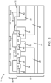
FIG. 2 is a cross-sectional view of the structure at a fabrication stage subsequent toFIG. 1 . -
FIG. 3 is a cross-sectional view of a structure in accordance with alternative embodiments of the invention. - With reference to
FIG. 1 and in accordance with embodiments of the invention, adevice structure 10 for an electrostatic discharge protection device includes asemiconductor substrate 12, adeep well 14, and shallowtrench isolation regions semiconductor substrate 12 may be comprised of a semiconductor material, such as single-crystal silicon, that is doped to have p-type conductivity. Thedeep well 14 is doped to have an opposite conductivity type from thesemiconductor substrate 12. In an embodiment, thedeep well 14 may contain a concentration of an n-type dopant (e.g., arsenic or phosphorus) such that thedeep well 14 has n-type conductivity. In an embodiment, thedeep well 14 may be formed by introducing a dopant by, for example, a masked ion implantation into thesemiconductor substrate 12. The implantation conditions (e.g., ion species, dose, kinetic energy) may be selected to tune the electrical and physical characteristics of thedeep well 14. The shallowtrench isolation regions semiconductor substrate 12 with lithography and etching processes, depositing a dielectric material, such as silicon dioxide, in the shallow trenches, and planarizing and/or recessing the deposited dielectric material. - Wells 24, 26 and
wells semiconductor substrate 12. A portion of thedeep well 14 is positioned in a lateral direction as a finger of oppositely-doped semiconductor material between thewell 24 and thewell 26. The finger portion of thedeep well 14 may extend in a vertical direction between thewell 28 and the well 30. Thewell 28 may be positioned in a vertical direction between thewell 24 and atop surface 16 of thesemiconductor substrate 12. Similarly, the well 30 may be positioned in a vertical direction between thewell 26 and thetop surface 16 of thesemiconductor substrate 12. Thedeep well 14 includes a portion positioned in a vertical direction between thewell 28 and thesemiconductor substrate 12 beneath thedeep well 14. Thedeep well 14 also includes another portion positioned in a vertical direction between thewell 30 and thesemiconductor substrate 12 beneath thedeep well 14. As a result, a singledeep well 14 electrically isolates thewells semiconductor substrate 12 beneath thedeep well 14 and eliminates the need for an extra guard ring. - In an embodiment, the
wells wells wells wells wells wells semiconductor substrate 12. The implantation conditions (e.g., ion species, dose, kinetic energy) may be selected to tune the electrical and physical characteristics of thewells wells wells semiconductor substrate 12. The implantation conditions (e.g., ion species, dose, kinetic energy) may be selected to tune the electrical and physical characteristics of thewells - Wells 32, 34 may be formed in the
semiconductor substrate 12. Thewell 32 includes a portion that overlaps with the finger portion of thedeep well 14 and a portion that overlaps with the oppositely-doped well 28. Thewell 34 includes a portion that overlaps with the finger portion of thedeep well 14 and a portion that overlaps with the oppositely-doped well 28. The shallowtrench isolation region 22 and the finger portion of thedeep well 14 are positioned in a lateral direction between thewell 32 and the well 34. A finger portion of thewell 28 and the shallowtrench isolation region 21 are disposed in a lateral direction between thewell 32 and the oppositely-doped well 24. A finger portion of thewell 30 is disposed in a lateral direction between thewell 34 and the oppositely-doped well 26. - The
wells deep well 14 and an opposite conductivity type from thewells wells wells deep well 14. Thewells wells semiconductor substrate 12. The implantation conditions (e.g., ion species, dose, kinetic energy) may be selected to tune the electrical and physical characteristics of thewells - A
doped region 38 is positioned in the well 24, adoped region 40 is positioned in thewell 34, and adoped region 42 is positioned in thewell 26. Thedoped region top surface 16 of thesemiconductor substrate 12. Thedoped region 38 and thedoped region 42 may be doped to the same conductivity type as thewells doped region 40 may be doped to have an opposite conductivity type from thewell 34. In an embodiment, thedoped regions regions regions semiconductor substrate 12. The implantation conditions (e.g., ion species, dose, kinetic energy) may be selected to tune the electrical and physical characteristics of the dopedregions - A doped
region 44 is positioned in the well 24, and a dopedregion 46 is positioned in thewell 32. The dopedregions top surface 16 of thesemiconductor substrate 12. The dopedregion 44 may be doped to have an opposite conductivity type from the well 24, and the dopedregion 46 may be doped to have the same conductivity type as the well 32 but at a higher dopant concentration. In an embodiment, the dopedregions regions regions semiconductor substrate 12. The implantation conditions (e.g., ion species, dose, kinetic energy) may be selected to tune the electrical and physical characteristics of the dopedregions trench isolation region 20 is positioned between the dopedregion 38 and the dopedregion 44. The shallowtrench isolation region 21 is positioned between the dopedregion 38 and the dopedregion 46. The shallowtrench isolation region 22 is positioned between the dopedregion 40 and the dopedregion 46. - The shallow
trench isolation region 20 is positioned in a lateral direction between the dopedregion 38 and the dopedregion 44, which are positioned adjacent to each other. The shallowtrench isolation region 21 is positioned in a lateral direction between the dopedregion 38 and the dopedregion 46, which are positioned adjacent to each other. The shallowtrench isolation region 22 is positioned in a lateral direction between the dopedregion 46 and the dopedregion 40, which are positioned adjacent to each other. - A
dielectric layer 48 may be formed on thetop surface 16 of thesemiconductor substrate 12. Thedielectric layer 48 may be comprised of a dielectric material, such as silicon nitride, that is deposited and then patterned by lithography and etching processes to form the sections. Thedielectric layer 48 has an overlapping relationship with a portion of the well 26, a portion of the well 34, and the finger portion of the well 30 that is disposed in a lateral direction between the portion of the well 26 and the portion of the well 34. In an alternative embodiment, thedielectric layer 48 may also overlap with all or a portion of the dopedregion 40 and with all or a portion of the dopedregion 42. Thedielectric layer 48 may function as a silicide-blocking layer. - With reference to
FIG. 2 in which like reference numerals refer to like features inFIG. 1 and at a subsequent fabrication stage, thedevice structure 10 may include aninterconnect structure 58 formed by middle-of-line processing and back-end-of-line processing. Theinterconnect structure 58 may includeelectrical connections electrical connections interconnect structure 58. - The
electrical connection 50 physically and electrically connects the dopedregion 38 and the dopedregion 44, which are adjacent to each other, to aground terminal 60. Theelectrical connection 52 physically and electrically connects the dopedregion 40 and the dopedregion 46, which are adjacent to each other, to an input/output terminal 62 that is protected by thedevice structure 10. In an embodiment, the input/output terminal 62 may be a power pad. Theelectrical connection 54 physically and electrically connects to the dopedregion 42 to a power (Vdd)terminal 64. The well 28 is coupled to theground terminal 60 by the well 24 and dopedregion 38, and the well 30 is coupled to thepower terminal 64 by the well 26 and the dopedregion 42. - The
device structure 10 may improve electrostatic discharge protection for the input/output terminal 62. The well 32, which is connected to the input/output terminal 62, includes a portion that overlaps with the well 28 of opposite conductivity type and a portion that overlaps with the finger portion of thedeep well 14 of the same conductivity type. The well 34 includes a portion that overlaps with the well 30 of opposite conductivity type and a portion that overlaps with the finger portion of thedeep well 14 of the same conductivity type. The dopedregion 38, which is connected to theground terminal 60, is positioned adjacent to the dopedregion 46 that is connected to the input/output terminal 62. The dopedregion 44, thewells region 40, the well 34, and thewells region 44, the dopedregion 38, the dopedregion 46, deep well 14, and the dopedregion 42 define a silicon-controlled rectifier device structure that is integrated with the NPN parasitic transistor and the PNP parasitic transistor. The silicon-controlled rectifier device structure of the electrostatic discharge protection device provides a local clamp between theground terminal 60 and thepower terminal 64. - With reference to
FIG. 3 in which like reference numerals refer to like features inFIG. 2 and in accordance with alternative embodiments of the invention, thedevice structure 10 may be modified to add a well 70 beneath the shallowtrench isolation region 22. The well 70 may be doped to have an opposite conductivity type from thewells deep well 14. The well 70 is positioned in a lateral direction between the well 32 and the well 34, and the well 70 is positioned in a vertical direction between the finger portion of thedeep well 14 and the shallowtrench isolation region 22. The well 70 is electrically isolated and floating in thedevice structure 10. In an embodiment, the well 70 may be formed when thewells wells - The methods as described above are used in the fabrication of integrated circuit chips. The resulting integrated circuit chips can be distributed by the fabricator in raw wafer form (e.g., as a single wafer that has multiple unpackaged chips), as a bare die, or in a packaged form. The chip may be integrated with other chips, discrete circuit elements, and/or other signal processing devices as part of either an intermediate product or an end product. The end product can be any product that includes integrated circuit chips, such as computer products having a central processor or smartphones.
- References herein to terms modified by language of approximation, such as "about", "approximately", and "substantially", are not to be limited to the precise value specified. The language of approximation may correspond to the precision of an instrument used to measure the value and, unless otherwise dependent on the precision of the instrument, may indicate a range of +/- 10% of the stated value(s).
- References herein to terms such as "vertical", "horizontal", etc. are made by way of example, and not by way of limitation, to establish a frame of reference. The term "horizontal" as used herein is defined as a plane parallel to a conventional plane of a semiconductor substrate, regardless of its actual three-dimensional spatial orientation. The terms "vertical" and "normal" refer to a direction in the frame of reference perpendicular to the horizontal, as just defined. The term "lateral" refers to a direction in the frame of reference within the horizontal plane.
- A feature "connected" or "coupled" to or with another feature may be directly connected or coupled to or with the other feature or, instead, one or more intervening features may be present. A feature may be "directly connected" or "directly coupled" to or with another feature if intervening features are absent. A feature may be "indirectly connected" or "indirectly coupled" to or with another feature if at least one intervening feature is present. A feature "on" or "contacting" another feature may be directly on or in direct contact with the other feature or, instead, one or more intervening features may be present. A feature may be "directly on" or in "direct contact" with another feature if intervening features are absent. A feature may be "indirectly on" or in "indirect contact" with another feature if at least one intervening feature is present. Different features may "overlap" if a feature extends over, and covers a part of, another feature.
- The descriptions of the various embodiments of the present invention have been presented for purposes of illustration but are not intended to be exhaustive or limited to the embodiments disclosed. Many modifications and variations will be apparent to those of ordinary skill in the art without departing from the scope and spirit of the described embodiments. The terminology used herein was chosen to best explain the principles of the embodiments, the practical application or technical improvement over technologies found in the marketplace, or to enable others of ordinary skill in the art to understand the embodiments disclosed herein.
- In summary, the following embodiments are explicitly disclosed.
- A structure for an electrostatic discharge protection device, the structure comprising:
- a semiconductor substrate;
- a first well in the semiconductor substrate, the first well having a first conductivity type;
- a second well in the semiconductor substrate, the second well having the first conductivity type;a third well in the semiconductor substrate, the third well having a second conductivity type, and the third well including a portion that overlaps with the first well; and
- a fourth well in the semiconductor substrate, the fourth well having the second conductivity type, and the fourth well including a portion that overlaps with the second well.
- The structure of embodiment 1, wherein the first conductivity type is p-type, and the second conductivity type is n-type.
- The structure of embodiment 1 or 2, further comprising:
- a power terminal,
- wherein the first well is connected to the power terminal.
- The structure of one of embodiments 1 to 3, further comprising:
- a ground terminal,
- wherein the second well is connected to the ground terminal.
- The structure of one of embodiments 1 to 4, further comprising:
- an input/output terminal; and
- a first doped region in the third well, the first doped region having the second conductivity type t a higher dopant concentration than the third well, and the first doped region connected to the input/output terminal.
- The structure of embodiment 5, further comprising:
- a ground terminal; and
- a second doped region coupling the first well to the ground terminal, the second doped region having the first conductivity type at a higher dopant concentration than the first well, and the second doped region positioned adjacent to the first doped region.
- The structure of embodiment 6, further comprising:
a shallow trench isolation region in the semiconductor substrate, the shallow trench isolation region arranged in a lateral direction between the first doped region and the second doped region. - The structure of embodiment 6 or 7, further comprising:
a third doped region in the fourth well, the third doped region having the first conductivity type, the third doped region positioned adjacent to the first doped region, and the third doped region connected to the input/output terminal. Herein, the third doped region may correspond to the third doped region of embodiment 7 in accordance with embodiment 8 referring back to embodiment 7. - The structure of one of embodiments 6 to 8, further comprising:
a third doped region adjacent to the second doped region, the third doped region having the second conductivity type, and the third doped region connected to the ground terminal. - The structure of one of embodiments 6 to 9, further comprising:
- a power terminal; and
- a third doped region coupling the second well to the power terminal, the third doped region having the first conductivity type.
- The structure of one of embodiments 5 to 10, further comprising:
a second doped region in the fourth well, the second doped region having the first conductivity type, the second doped region positioned adjacent to the first doped region, and the second doped region connected to the input/output terminal. Herein, the second doped region may correspond to the second doped region of embodiment 6 in accordance with embodiment 11 referring back to embodiment 6. - The structure of one of embodiments 1 to 11, further comprising:
a fifth well in the semiconductor substrate, the fifth well having the second conductivity type, and the fifth well including a portion positioned between the first well and the second well. - The structure of
embodiment 12, wherein the third well and the fourth well contain a higher dopant concentration than the fifth well. - The structure of
embodiment 12 or 13, wherein the portion of the fifth well extends between the third well and the fourth well. - The structure of one of
embodiments 12 to 14, further comprising:
a shallow trench isolation region in the semiconductor substrate, the shallow trench isolation region positioned over the portion of the fifth well. Herein, the shallow trench isolation may correspond to the shallow trench isolation of embodiment 7 in accordance with embodiment 15 being referred back to embodiment 7. - The structure of one of embodiments 1 to 15, wherein the semiconductor substrate has a top surface, and further comprising:
a fifth well in the semiconductor substrate, the fifth well having the second conductivity type, the first well positioned in a vertical direction between a first portion of the fifth well and the top surface of the semiconductor substrate, and the second well positioned in the vertical direction between a second portion of the fifth well and the top surface of the semiconductor substrate. - Herein, the fifth well may correspond to the fifth well of
embodiment 12 in accordance withembodiment 16 referring back toembodiment 12. - The structure of
embodiment 16, wherein the fifth well includes a third portion positioned in a lateral direction between the first well and the second well. - The structure of one of embodiments 1 to 17, further comprising:
a fifth well in the semiconductor substrate, the fifth well having the first conductivity type, and the fifth well positioned between the third well and the fourth well. Herein, the fifth well may correspond to the fifth well ofembodiment 12 and/or 16 in accordance with embodiment 18 referring back toembodiment 12 and/or 16. - The structure of embodiment 18, wherein the semiconductor substrate has a top surface, and further comprising:
a shallow trench isolation region in the semiconductor substrate, the shallow trench isolation region positioned between the fifth well and the top surface of the semiconductor substrate. - Herein, the shallow trench isolation may correspond to the shallow trench isolation of embodiment 7 and/or 15 in accordance with embodiment 19 being referred back to embodiment 7 and/or 15.
- A method of forming a structure for an electrostatic discharge protection device, the method comprising:
- forming a first well and a second well in a semiconductor substrate, wherein the first well and the second well have a first conductivity type; and
- forming a third well and a fourth well in the semiconductor substrate, wherein the third well and the fourth well have a second conductivity type, the third well includes a portion that overlaps with the first well, and the fourth well includes a portion that overlaps with the second well.
- The method of
embodiment 20, wherein the structure of one of embodiments 1 to 19 is formed. At least in the embodiments above, the term "include" and its variants may be interpreted as meaning that an embodiment includes stated features, while not necessarily excluding the presence of other features that are not explicitly stated.
Claims (15)
- A structure for an electrostatic discharge protection device, the structure comprising:a semiconductor substrate;a first well in the semiconductor substrate, the first well having a first conductivity type;a second well in the semiconductor substrate, the second well having the first conductivity type;a third well in the semiconductor substrate, the third well having a second conductivity type, and the third well including a portion that overlaps with the first well; anda fourth well in the semiconductor substrate, the fourth well having the second conductivity type, and the fourth well including a portion that overlaps with the second well.
- The structure of claim 1, wherein the first conductivity type is p-type, and the second conductivity type is n-type.
- The structure of claim 1 or 2, further comprising:a power terminal, wherein the first well is connected to the power terminal, and/ora ground terminal, wherein the second well is connected to the ground terminal.
- The structure of one of claims 1 to 3, further comprising:an input/output terminal; anda first doped region in the third well, the first doped region having the second conductivity type at a higher dopant concentration than the third well, and the first doped region connected to the input/output terminal.
- The structure of claim 4, further comprising:a ground terminal; anda second doped region coupling the first well to the ground terminal, the second doped region having the first conductivity type at a higher dopant concentration than the first well, and the second doped region positioned adjacent to the first doped region.
- The structure of claim 5, further comprising:a shallow trench isolation region in the semiconductor substrate, the shallow trench isolation region arranged in a lateral direction between the first doped region and the second doped region, and/ora power terminal and a third doped region coupling the second well to the power terminal, the third doped region having the first conductivity type
- The structure of claim 5 or 6, further comprising a third doped region, wherein at least one of:the third doped region is in the fourth well, the third doped region having the first conductivity type, the third doped region positioned adjacent to the first doped region, and the third doped region connected to the input/output terminal; andthe third doped region is adjacent to the second doped region, the third doped region having the second conductivity type, and the third doped region connected to the ground terminal.
- The structure of one of claims 4 to 7, further comprising:
a second doped region in the fourth well, the second doped region having the first conductivity type, the second doped region positioned adjacent to the first doped region, and the second doped region connected to the input/output terminal. - The structure of one of claims 1 to 8 further comprising:
a fifth well in the semiconductor substrate, the fifth well having the second conductivity type, and the fifth well including a portion positioned between the first well and the second well. - The structure of claim 9,wherein the third well and the fourth well contain a higher dopant concentration than the fifth well; and/orwherein the portion of the fifth well extends between the third well and the fourth well; and/orwherein the structure further comprises a shallow trench isolation region in the semiconductor substrate, the shallow trench isolation region positioned over the portion of the fifth well.
- The structure of one of claims 1 to 10, wherein the semiconductor substrate has a top surface, and further comprising:
a fifth well in the semiconductor substrate, the fifth well having the second conductivity type, the first well positioned in a vertical direction between a first portion of the fifth well and the top surface of the semiconductor substrate, and the second well positioned in the vertical direction between a second portion of the fifth well and the top surface of the semiconductor substrate. - The structure of claim 11, wherein the fifth well includes a third portion positioned in a lateral direction between the first well and the second well.
- The structure of one of claims 1 to 10, further comprising:
a fifth well in the semiconductor substrate, the fifth well having the first conductivity type, and the fifth well positioned between the third well and the fourth well. - The structure of claim 13, wherein the semiconductor substrate has a top surface, and further comprising:
a shallow trench isolation region in the semiconductor substrate, the shallow trench isolation region positioned between the fifth well and the top surface of the semiconductor substrate. - A method of forming a structure for an electrostatic discharge protection device, the method comprising:forming a first well and a second well in a semiconductor substrate, wherein the first well and the second well have a first conductivity type; andforming a third well and a fourth well in the semiconductor substrate, wherein the third well and the fourth well have a second conductivity type, the third well includes a portion that overlaps with the first well, and the fourth well includes a portion that overlaps with the second well.
Applications Claiming Priority (1)
| Application Number | Priority Date | Filing Date | Title |
|---|---|---|---|
| US18/086,938 US12471386B2 (en) | 2022-12-22 | 2022-12-22 | Electrostatic discharge protection devices |
Publications (1)
| Publication Number | Publication Date |
|---|---|
| EP4391055A1 true EP4391055A1 (en) | 2024-06-26 |
Family
ID=88097375
Family Applications (1)
| Application Number | Title | Priority Date | Filing Date |
|---|---|---|---|
| EP23198265.3A Pending EP4391055A1 (en) | 2022-12-22 | 2023-09-19 | Electrostatic discharge protection devices |
Country Status (3)
| Country | Link |
|---|---|
| US (1) | US12471386B2 (en) |
| EP (1) | EP4391055A1 (en) |
| CN (1) | CN118248679A (en) |
Families Citing this family (1)
| Publication number | Priority date | Publication date | Assignee | Title |
|---|---|---|---|---|
| CN119208321B (en) * | 2024-09-18 | 2025-10-17 | 联合微电子中心有限责任公司 | Electrostatic protection device, preparation method and electronic product |
Citations (2)
| Publication number | Priority date | Publication date | Assignee | Title |
|---|---|---|---|---|
| US6960792B1 (en) * | 2003-09-30 | 2005-11-01 | National Semiconductor Corporation | Bi-directional silicon controlled rectifier structure with high holding voltage for latchup prevention |
| US20060145260A1 (en) * | 2004-12-30 | 2006-07-06 | Magnachip Semiconductor Ltd. | Electro-static discharge protection circuit and method for fabricating the same |
Family Cites Families (8)
| Publication number | Priority date | Publication date | Assignee | Title |
|---|---|---|---|---|
| US6011681A (en) | 1998-08-26 | 2000-01-04 | Taiwan Semiconductor Manufacturing Company, Ltd. | Whole-chip ESD protection for CMOS ICs using bi-directional SCRs |
| TW560038B (en) | 2002-05-29 | 2003-11-01 | Ind Tech Res Inst | Electrostatic discharge protection circuit using whole chip trigger technique |
| US7202114B2 (en) | 2004-01-13 | 2007-04-10 | Intersil Americas Inc. | On-chip structure for electrostatic discharge (ESD) protection |
| US8039868B2 (en) | 2008-12-23 | 2011-10-18 | International Business Machines Corporation | Structure and method for an electrostatic discharge (ESD) silicon controlled rectifier (SCR) structure |
| US8169760B2 (en) | 2009-01-19 | 2012-05-01 | International Business Machines Corporation | Signal and power supply integrated ESD protection device |
| US8860080B2 (en) | 2012-12-19 | 2014-10-14 | Analog Devices, Inc. | Interface protection device with integrated supply clamp and method of forming the same |
| US20170018612A1 (en) * | 2015-07-14 | 2017-01-19 | Broadcom Corporation | Split-gate devices |
| TWI765166B (en) * | 2019-07-16 | 2022-05-21 | 源芯半導體股份有限公司 | Transient voltage suppression device |
-
2022
- 2022-12-22 US US18/086,938 patent/US12471386B2/en active Active
-
2023
- 2023-09-19 EP EP23198265.3A patent/EP4391055A1/en active Pending
- 2023-11-20 CN CN202311544006.0A patent/CN118248679A/en active Pending
Patent Citations (2)
| Publication number | Priority date | Publication date | Assignee | Title |
|---|---|---|---|---|
| US6960792B1 (en) * | 2003-09-30 | 2005-11-01 | National Semiconductor Corporation | Bi-directional silicon controlled rectifier structure with high holding voltage for latchup prevention |
| US20060145260A1 (en) * | 2004-12-30 | 2006-07-06 | Magnachip Semiconductor Ltd. | Electro-static discharge protection circuit and method for fabricating the same |
Also Published As
| Publication number | Publication date |
|---|---|
| CN118248679A (en) | 2024-06-25 |
| US12471386B2 (en) | 2025-11-11 |
| US20240213240A1 (en) | 2024-06-27 |
Similar Documents
| Publication | Publication Date | Title |
|---|---|---|
| US10692852B2 (en) | Silicon-controlled rectifiers with wells laterally isolated by trench isolation regions | |
| WO2008152026A2 (en) | Vertical current controlled silicon on insulator (soi) device and method of forming same | |
| US11476244B2 (en) | Laterally-diffused metal-oxide-semiconductor devices for electrostatic discharge protection applications | |
| TWI585956B (en) | Grounding system for integrated circuits for special applications of circuits incorporating back-illuminated photosensor arrays | |
| US12446322B2 (en) | Electrostatic discharge protection devices including a silicon-controlled rectifier | |
| US12471386B2 (en) | Electrostatic discharge protection devices | |
| US12471385B2 (en) | Electrostatic discharge protection devices with multiple-depth trench isolation | |
| US12581746B2 (en) | Silicon-controlled rectifiers for electrostatic discharge protection | |
| US6894321B2 (en) | ESD protection circuit with plural thyristors | |
| US20250031457A1 (en) | Self-protected electrostatic discharge protection devices | |
| US11935946B2 (en) | Silicon-controlled rectifiers in a silicon-on-insulator technology | |
| US20240079482A1 (en) | Gated protection device structures for an electrostatic discharge protection circuit | |
| US11848388B1 (en) | Silicon-controlled rectifiers for electrostatic discharge protection | |
| US11776952B1 (en) | Silicon-controlled rectifiers for an electrostatic discharge protection device | |
| US12575189B2 (en) | Silicon-controlled rectifiers with a segmented floating region | |
| EP4539122A1 (en) | Multiple-depth trench isolation for electrostatic discharge protection devices | |
| US20240429227A1 (en) | Structures for an electrostatic discharge protection device | |
| US12408366B2 (en) | Protection device structures with a discontinuous isolation well | |
| US20240145462A1 (en) | Electrostatic discharge control devices | |
| HK1223734B (en) | Integrated circuit grounding system for backside illuminated optical sensors |
Legal Events
| Date | Code | Title | Description |
|---|---|---|---|
| PUAI | Public reference made under article 153(3) epc to a published international application that has entered the european phase |
Free format text: ORIGINAL CODE: 0009012 |
|
| STAA | Information on the status of an ep patent application or granted ep patent |
Free format text: STATUS: REQUEST FOR EXAMINATION WAS MADE |
|
| 17P | Request for examination filed |
Effective date: 20230919 |
|
| AK | Designated contracting states |
Kind code of ref document: A1 Designated state(s): AL AT BE BG CH CY CZ DE DK EE ES FI FR GB GR HR HU IE IS IT LI LT LU LV MC ME MK MT NL NO PL PT RO RS SE SI SK SM TR |
|
| STAA | Information on the status of an ep patent application or granted ep patent |
Free format text: STATUS: EXAMINATION IS IN PROGRESS |
|
| 17Q | First examination report despatched |
Effective date: 20251029 |