EP4391007A1 - Pole piece incorporating optical cavity for improved phase-contrast in electron microscope imaging - Google Patents
Pole piece incorporating optical cavity for improved phase-contrast in electron microscope imaging Download PDFInfo
- Publication number
- EP4391007A1 EP4391007A1 EP23215745.3A EP23215745A EP4391007A1 EP 4391007 A1 EP4391007 A1 EP 4391007A1 EP 23215745 A EP23215745 A EP 23215745A EP 4391007 A1 EP4391007 A1 EP 4391007A1
- Authority
- EP
- European Patent Office
- Prior art keywords
- central axis
- pole piece
- lateral
- aperture
- section
- Prior art date
- Legal status (The legal status is an assumption and is not a legal conclusion. Google has not performed a legal analysis and makes no representation as to the accuracy of the status listed.)
- Pending
Links
- 230000003287 optical effect Effects 0.000 title claims description 111
- 238000003384 imaging method Methods 0.000 title claims description 18
- 230000001976 improved effect Effects 0.000 title abstract description 8
- 238000000034 method Methods 0.000 claims abstract description 35
- 150000001875 compounds Chemical class 0.000 claims description 4
- 239000002245 particle Substances 0.000 abstract description 11
- 230000005855 radiation Effects 0.000 description 47
- 239000000523 sample Substances 0.000 description 44
- 238000010586 diagram Methods 0.000 description 30
- 238000005286 illumination Methods 0.000 description 19
- 230000008569 process Effects 0.000 description 16
- 238000004458 analytical method Methods 0.000 description 12
- 239000012472 biological sample Substances 0.000 description 10
- 230000010363 phase shift Effects 0.000 description 10
- 230000003993 interaction Effects 0.000 description 9
- 230000014759 maintenance of location Effects 0.000 description 8
- 239000012620 biological material Substances 0.000 description 7
- 230000005540 biological transmission Effects 0.000 description 7
- 230000001965 increasing effect Effects 0.000 description 7
- 239000000463 material Substances 0.000 description 7
- 238000001000 micrograph Methods 0.000 description 7
- 230000005670 electromagnetic radiation Effects 0.000 description 6
- 238000003917 TEM image Methods 0.000 description 5
- 238000013459 approach Methods 0.000 description 5
- 230000008878 coupling Effects 0.000 description 5
- 238000010168 coupling process Methods 0.000 description 5
- 238000005859 coupling reaction Methods 0.000 description 5
- 238000010894 electron beam technology Methods 0.000 description 5
- 238000001493 electron microscopy Methods 0.000 description 4
- 230000007246 mechanism Effects 0.000 description 4
- 230000002906 microbiologic effect Effects 0.000 description 4
- 230000004048 modification Effects 0.000 description 4
- 238000012986 modification Methods 0.000 description 4
- 230000004075 alteration Effects 0.000 description 3
- 239000012141 concentrate Substances 0.000 description 3
- 238000000604 cryogenic transmission electron microscopy Methods 0.000 description 3
- 230000006870 function Effects 0.000 description 3
- 238000004452 microanalysis Methods 0.000 description 3
- 238000000386 microscopy Methods 0.000 description 3
- 238000001350 scanning transmission electron microscopy Methods 0.000 description 3
- IJGRMHOSHXDMSA-UHFFFAOYSA-N Atomic nitrogen Chemical compound N#N IJGRMHOSHXDMSA-UHFFFAOYSA-N 0.000 description 2
- XEEYBQQBJWHFJM-UHFFFAOYSA-N Iron Chemical compound [Fe] XEEYBQQBJWHFJM-UHFFFAOYSA-N 0.000 description 2
- 239000013078 crystal Substances 0.000 description 2
- 230000000694 effects Effects 0.000 description 2
- 230000005672 electromagnetic field Effects 0.000 description 2
- 230000014509 gene expression Effects 0.000 description 2
- 238000002173 high-resolution transmission electron microscopy Methods 0.000 description 2
- 230000001771 impaired effect Effects 0.000 description 2
- 238000011065 in-situ storage Methods 0.000 description 2
- 230000000977 initiatory effect Effects 0.000 description 2
- 230000010354 integration Effects 0.000 description 2
- 239000011368 organic material Substances 0.000 description 2
- 238000002135 phase contrast microscopy Methods 0.000 description 2
- 230000035945 sensitivity Effects 0.000 description 2
- 239000007787 solid Substances 0.000 description 2
- 238000003860 storage Methods 0.000 description 2
- 238000011144 upstream manufacturing Methods 0.000 description 2
- 241000894006 Bacteria Species 0.000 description 1
- OKTJSMMVPCPJKN-UHFFFAOYSA-N Carbon Chemical compound [C] OKTJSMMVPCPJKN-UHFFFAOYSA-N 0.000 description 1
- 206010010071 Coma Diseases 0.000 description 1
- 238000010521 absorption reaction Methods 0.000 description 1
- 230000003213 activating effect Effects 0.000 description 1
- 230000003190 augmentative effect Effects 0.000 description 1
- 230000008901 benefit Effects 0.000 description 1
- 239000002041 carbon nanotube Substances 0.000 description 1
- 229910021393 carbon nanotube Inorganic materials 0.000 description 1
- 238000012512 characterization method Methods 0.000 description 1
- 238000004891 communication Methods 0.000 description 1
- 238000004590 computer program Methods 0.000 description 1
- 238000012937 correction Methods 0.000 description 1
- 239000002178 crystalline material Substances 0.000 description 1
- 230000003247 decreasing effect Effects 0.000 description 1
- 238000005315 distribution function Methods 0.000 description 1
- 238000005430 electron energy loss spectroscopy Methods 0.000 description 1
- 230000007613 environmental effect Effects 0.000 description 1
- 230000004907 flux Effects 0.000 description 1
- 239000012634 fragment Substances 0.000 description 1
- 230000008014 freezing Effects 0.000 description 1
- 238000007710 freezing Methods 0.000 description 1
- PCHJSUWPFVWCPO-UHFFFAOYSA-N gold Chemical compound [Au] PCHJSUWPFVWCPO-UHFFFAOYSA-N 0.000 description 1
- 239000010931 gold Substances 0.000 description 1
- 229910052737 gold Inorganic materials 0.000 description 1
- 230000001939 inductive effect Effects 0.000 description 1
- 229910010272 inorganic material Inorganic materials 0.000 description 1
- 239000011147 inorganic material Substances 0.000 description 1
- 238000003780 insertion Methods 0.000 description 1
- 230000037431 insertion Effects 0.000 description 1
- 230000002452 interceptive effect Effects 0.000 description 1
- 239000011229 interlayer Substances 0.000 description 1
- 238000010884 ion-beam technique Methods 0.000 description 1
- 150000002500 ions Chemical class 0.000 description 1
- 229910052742 iron Inorganic materials 0.000 description 1
- 230000000670 limiting effect Effects 0.000 description 1
- 239000007788 liquid Substances 0.000 description 1
- 238000004519 manufacturing process Methods 0.000 description 1
- 238000005259 measurement Methods 0.000 description 1
- 239000002184 metal Substances 0.000 description 1
- 229910052751 metal Inorganic materials 0.000 description 1
- 239000002086 nanomaterial Substances 0.000 description 1
- 229910052757 nitrogen Inorganic materials 0.000 description 1
- 238000000399 optical microscopy Methods 0.000 description 1
- 230000036961 partial effect Effects 0.000 description 1
- 230000035699 permeability Effects 0.000 description 1
- 230000000704 physical effect Effects 0.000 description 1
- 238000012545 processing Methods 0.000 description 1
- 230000000750 progressive effect Effects 0.000 description 1
- 102000004169 proteins and genes Human genes 0.000 description 1
- 108090000623 proteins and genes Proteins 0.000 description 1
- 230000002829 reductive effect Effects 0.000 description 1
- 230000002441 reversible effect Effects 0.000 description 1
- 238000000926 separation method Methods 0.000 description 1
- 238000007493 shaping process Methods 0.000 description 1
- 238000001228 spectrum Methods 0.000 description 1
- 230000004936 stimulating effect Effects 0.000 description 1
- 239000000758 substrate Substances 0.000 description 1
- 238000012546 transfer Methods 0.000 description 1
- 230000003612 virological effect Effects 0.000 description 1
- 238000012800 visualization Methods 0.000 description 1
Images




Classifications
-
- H—ELECTRICITY
- H01—ELECTRIC ELEMENTS
- H01J—ELECTRIC DISCHARGE TUBES OR DISCHARGE LAMPS
- H01J37/00—Discharge tubes with provision for introducing objects or material to be exposed to the discharge, e.g. for the purpose of examination or processing thereof
- H01J37/02—Details
- H01J37/04—Arrangements of electrodes and associated parts for generating or controlling the discharge, e.g. electron-optical arrangement or ion-optical arrangement
- H01J37/10—Lenses
- H01J37/14—Lenses magnetic
-
- H—ELECTRICITY
- H01—ELECTRIC ELEMENTS
- H01J—ELECTRIC DISCHARGE TUBES OR DISCHARGE LAMPS
- H01J37/00—Discharge tubes with provision for introducing objects or material to be exposed to the discharge, e.g. for the purpose of examination or processing thereof
- H01J37/02—Details
- H01J37/04—Arrangements of electrodes and associated parts for generating or controlling the discharge, e.g. electron-optical arrangement or ion-optical arrangement
- H01J37/147—Arrangements for directing or deflecting the discharge along a desired path
- H01J37/15—External mechanical adjustment of electron or ion optical components
-
- H—ELECTRICITY
- H01—ELECTRIC ELEMENTS
- H01J—ELECTRIC DISCHARGE TUBES OR DISCHARGE LAMPS
- H01J37/00—Discharge tubes with provision for introducing objects or material to be exposed to the discharge, e.g. for the purpose of examination or processing thereof
- H01J37/02—Details
- H01J37/04—Arrangements of electrodes and associated parts for generating or controlling the discharge, e.g. electron-optical arrangement or ion-optical arrangement
- H01J37/10—Lenses
- H01J37/14—Lenses magnetic
- H01J37/141—Electromagnetic lenses
-
- H—ELECTRICITY
- H01—ELECTRIC ELEMENTS
- H01J—ELECTRIC DISCHARGE TUBES OR DISCHARGE LAMPS
- H01J37/00—Discharge tubes with provision for introducing objects or material to be exposed to the discharge, e.g. for the purpose of examination or processing thereof
- H01J37/02—Details
- H01J37/20—Means for supporting or positioning the object or the material; Means for adjusting diaphragms or lenses associated with the support
-
- H—ELECTRICITY
- H01—ELECTRIC ELEMENTS
- H01J—ELECTRIC DISCHARGE TUBES OR DISCHARGE LAMPS
- H01J37/00—Discharge tubes with provision for introducing objects or material to be exposed to the discharge, e.g. for the purpose of examination or processing thereof
- H01J37/02—Details
- H01J37/22—Optical, image processing or photographic arrangements associated with the tube
-
- H—ELECTRICITY
- H01—ELECTRIC ELEMENTS
- H01J—ELECTRIC DISCHARGE TUBES OR DISCHARGE LAMPS
- H01J37/00—Discharge tubes with provision for introducing objects or material to be exposed to the discharge, e.g. for the purpose of examination or processing thereof
- H01J37/26—Electron or ion microscopes; Electron or ion diffraction tubes
- H01J37/261—Details
-
- H—ELECTRICITY
- H01—ELECTRIC ELEMENTS
- H01J—ELECTRIC DISCHARGE TUBES OR DISCHARGE LAMPS
- H01J37/00—Discharge tubes with provision for introducing objects or material to be exposed to the discharge, e.g. for the purpose of examination or processing thereof
- H01J37/26—Electron or ion microscopes; Electron or ion diffraction tubes
- H01J37/261—Details
- H01J37/263—Contrast, resolution or power of penetration
-
- H—ELECTRICITY
- H01—ELECTRIC ELEMENTS
- H01J—ELECTRIC DISCHARGE TUBES OR DISCHARGE LAMPS
- H01J37/00—Discharge tubes with provision for introducing objects or material to be exposed to the discharge, e.g. for the purpose of examination or processing thereof
- H01J37/26—Electron or ion microscopes; Electron or ion diffraction tubes
- H01J37/28—Electron or ion microscopes; Electron or ion diffraction tubes with scanning beams
-
- G—PHYSICS
- G01—MEASURING; TESTING
- G01N—INVESTIGATING OR ANALYSING MATERIALS BY DETERMINING THEIR CHEMICAL OR PHYSICAL PROPERTIES
- G01N23/00—Investigating or analysing materials by the use of wave or particle radiation, e.g. X-rays or neutrons, not covered by groups G01N3/00 – G01N17/00, G01N21/00 or G01N22/00
- G01N23/02—Investigating or analysing materials by the use of wave or particle radiation, e.g. X-rays or neutrons, not covered by groups G01N3/00 – G01N17/00, G01N21/00 or G01N22/00 by transmitting the radiation through the material
- G01N23/04—Investigating or analysing materials by the use of wave or particle radiation, e.g. X-rays or neutrons, not covered by groups G01N3/00 – G01N17/00, G01N21/00 or G01N22/00 by transmitting the radiation through the material and forming images of the material
- G01N23/041—Phase-contrast imaging, e.g. using grating interferometers
-
- H—ELECTRICITY
- H01—ELECTRIC ELEMENTS
- H01F—MAGNETS; INDUCTANCES; TRANSFORMERS; SELECTION OF MATERIALS FOR THEIR MAGNETIC PROPERTIES
- H01F3/00—Cores, Yokes, or armatures
- H01F3/10—Composite arrangements of magnetic circuits
-
- H—ELECTRICITY
- H01—ELECTRIC ELEMENTS
- H01J—ELECTRIC DISCHARGE TUBES OR DISCHARGE LAMPS
- H01J2237/00—Discharge tubes exposing object to beam, e.g. for analysis treatment, etching, imaging
- H01J2237/10—Lenses
- H01J2237/14—Lenses magnetic
- H01J2237/1405—Constructional details
- H01J2237/1415—Bores or yokes, i.e. magnetic circuit in general
-
- H—ELECTRICITY
- H01—ELECTRIC ELEMENTS
- H01J—ELECTRIC DISCHARGE TUBES OR DISCHARGE LAMPS
- H01J2237/00—Discharge tubes exposing object to beam, e.g. for analysis treatment, etching, imaging
- H01J2237/26—Electron or ion microscopes
- H01J2237/2614—Holography or phase contrast, phase related imaging in general, e.g. phase plates
Definitions
- Embodiments of the present disclosure are directed to electron microscopy components, systems, and methods. In particular, some embodiments are directed toward components configured for improved contrast in electron microscope images.
- Electron microscopy of biological samples involves exposure of organic materials to a beam of electrons. Interaction between electrons and the sample generates different types of detectable signals that can be used for imaging and analysis.
- TEMs transmission electron microscopes
- detailed information can be developed at the atomic scale, including images of the internal structures of biological materials, conformational information, and in-situ observations of microbiological processes.
- Embodiments of the present disclosure include a transmission electron microscope incorporating a lower pole piece configured to receive, include, and/or incorporate an optical cavity or components of an optical cavity.
- the optical cavity can be configured to concentrate electromagnetic radiation onto a beam of electrons at a position substantially corresponding to a first diffraction plane of the beam of electrons.
- the optical cavity can keep the area of the beam of electrons free of optical elements or other material.
- the lower pole piece can include a central aperture and multiple lateral apertures configured to accommodate the optical cavity and to permit EM radiation to be provided to the optical cavity from a radiation source external to the lower pole piece.
- Electron microscopy of biological samples involves exposure of biomaterials to a beam of electrons. Interaction between electrons and the sample generates different types of detectable signals that can be used for imaging and analysis.
- TEMs transmission electron microscopes
- detailed information can be developed at the atomic scale, including images of the internal structures of biological materials, conformations of biomolecules, and in-situ observations of microbiological processes.
- TEM analysis of biological materials at progressively smaller length scales, such as those on the order of ones to tens of Angstroms introduces challenges in differentiating structures of interest from background signals or imaging artifacts, due at least in part on the relatively low proportion of electrons that are scattered by biological samples. For at least these reasons, there is a need to develop components, systems, and methods for improved contrast in electron microscope images, for example, in the field of cryogenic TEM analysis of biological materials that exhibit sensitivity to radiation dose and a characteristic low signal-to-noise quality.
- a biological sample e.g., a protein particle, cell or cell fragment, viral particle, bacteria-derived materials, or the like
- freezing e.g., liquid nitrogen temperatures
- Organic materials from which biological samples are typically composed scatter a relatively small fraction of incident electrons (e.g., as opposed to heavier elements like iron, gold, or the like). In consequence, background information is typically significant and limits contrast in TEM images of biological samples.
- electron beam microanalysis that is routinely used in inorganic materials, such as crystal diffraction patterns (e.g., used to identify phase structures of semiconducting or metallic crystalline materials) is inhibited by relatively weak signal-to-background information.
- Approaches including, but not limited to, dark field TEM and Zernike Phase Contrast TEM modes can be used to reduce the relative proportion of background illumination and to increase the relative signal from scattered electrons in TEM images.
- phase-contrast microscopy In the field of optical microscopy, resolved images of microbiological samples, which scatter a relatively small proportion of incident photons, can be improved through the use of phase-contrast microscopy.
- An operative principle of phase-contrast microscopy is to differentiate between photons that have been scattered by a sample and photons that have passed through the sample without scattering.
- scattering refers to an interaction between a photon and an atom of the sample that results in a phase shift of scattered photons.
- optical elements e.g., condenser annulus, phase shift ring, and filter ring elements
- Electromagnetic radiation can be used to manipulate the beam of electrons generated in the TEM.
- stimulated Compton scattering can be induced in a beam of electrons by exposure to electromagnetic radiation (e.g., a continuous wave laser, a pulsed laser, x-rays, or the like).
- electromagnetic radiation e.g., a continuous wave laser, a pulsed laser, x-rays, or the like.
- the electron can undergo a phase shift.
- a continuous wave laser can be directed into a resonant optical cavity. This principle can be used to achieve phase-contrast TEM, but its application is limited, at least in part because the size of the optical cavity is constrained and because of the limited space available in proximity to the electron beam.
- One approach to increase contrast of nanostructured materials composed principally of light elements is to defocus the beam of electrons prior to incidence with the sample and applying EM radiation to the beam of electrons of suitable intensity at a position of a diffraction plane, thereby stimulating Compton scattering.
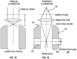
- This mode of illumination is referred to in the forthcoming paragraphs as "divergent illumination,” and described in reference to FIG. 1E .
- Such techniques permit, for example, visualization and measurement of interlayer spacings in carbon nanotubes and organic crystals that include a regular structure. Under divergent illumination, a first diffraction plane of the electron beam occurs at a point part-way between an upper surface and a lower surface of a lower pole piece forming a part of the objective section of the TEM, as described in more detail in reference to FIG.
- apertures formed in the body to facilitate moving optical components into or out of the central aperture of the lower pole piece can lower the threshold maximum ampere-turns of the lens coil at which magnetic saturation of the pole piece material occurs.
- shape, position, and orientation of the apertures is constrained by the position of the first diffraction plane and the angle of the optical cavity relative to a central axis of the lower pole piece.
- size of the central aperture of the lower pole piece which can be constrained by the inclusion of electromechanical alignment components, can introduce issues with maintaining vacuum integrity of the objective section and a liner tube of the TEM. In this way, configuring the lower pole piece to accept an optical cavity implicates multiple structural modifications to the lower pole piece that would not be used for other applications, such as vacuum system integration.
- FIG. 1A is a schematic diagram illustrating an example transmission electron microscope (TEM) system 100, in accordance with some embodiments of the present disclosure.
- TEM transmission electron microscope
- the example TEM system 100 includes an electron gun section, a TEM column including an objective section 120, and an imaging section.
- the present disclosure focuses on the objective section 120.
- the electron gun section includes electronics configured to energize an electron source, which can include a high-voltage field-emission source or other sources of emitted electrons, such that a beam of electrons is formed and conducted through a vacuum into the TEM column.
- the TEM column includes components for beam forming, including electromagnetic lenses 125 and multiple apertures to control properties of the beam of electrons.
- TEM column components include condenser lenses, objective lenses, projector lenses, among others, as well as corresponding apertures.
- the imaging section includes one or more types of detectors, sensors, screens, and/or optics configured to generate images, spectra, and other data for use in sample analysis.
- the imaging section can include a scintillator screen, binoculars, scanning transmission electron microscopy (STEM) detector(s), camera(s), electron energy loss spectroscopy (EELS) detectors, among others.
- STEM scanning transmission electron microscopy
- EELS electron energy loss spectroscopy
- FIG. 1B is a schematic diagram illustrating an example objective section 120 of a transmission electron microscope including components used for analysis of cryogenic samples, in accordance with some embodiments of the present disclosure.
- FIG. 1B omits some elements of the objective section illustrated in FIG. 1A , such as the vacuum enclosure, to focus description on components of the TEM 100 that interact with a beam of electrons.
- the example objective section 120 includes an upper pole piece, and a lower pole piece, a sample holder, and an objective aperture.
- the objective section also includes components for use in imaging and/or analysis of cryogenic samples, such as a cryoshield.
- the TEM 100 can be configured for automated serial analysis of multiple samples by including an automated sample loader.
- the volume available for integrating an optical cavity between the upper pole piece and the lower pole piece is limited by a lateral dimension "R” and a vertical dimension "Z,” where “lateral” refers to a direction substantially normal to the beam axis, A, and “vertical” refers to a direction substantially parallel to the beam axis A.
- the term “substantially” is used to indicate that deviation in the angle between laterally oriented or vertically oriented components relative to the beam axis, A, can occur within the scope of the present disclosure.
- one possible approach is to introduce the optical cavity between the lower pole piece and the sample holder.
- dimensions R and Z define the available volume between upper pole piece and lower pole piece for introduction of an optical cavity.
- the vertical dimension Z can be from about 3 mm to about 25 mm, with different vertical dimensions being used for different types of analysis.
- the lateral dimension R can be from about 10 mm to about 15 mm, although in some cases optical components and/or retention components can be disposed outside of the volume at the cost of increased complexity of the optical system.
- the sample holder is substantially centered with respect to the vertical dimension Z.
- the vertical space available for an optical cavity, between the sample holder and the lower pole piece can be from about 2 mm to about 4 mm.
- Horizontal space reserved for the electron beam implicates a lateral distance of 1 mm - 5 mm in the R dimension to be kept free of optical components.
- space constraints are greater, with space in the vertical dimension Z being limited to 1.5 mm or less (e.g., in some cases, no space is available). In this way, space limitations prevent the use of the optical cavity between the sample holder and the lower pole piece.
- the optical cavity can be introduced into the lower pole itself, as described in more detail in reference to FIGs. 1E - 4 .
- FIG. 1C is a schematic diagram illustrating an example optical cavity 140, in accordance with some embodiments of the present disclosure.
- the example optical cavity 140 is configured to be integrated into a lower pole piece of an electron microscope, such as the TEM 100 of FIG. 1 .
- interaction of electromagnetic (EM) radiation 150 with a beam of electrons 155 is induced by passing the beam of electrons 155 through a focal area of EM radiation 150 that is recirculated in the optical cavity 140.
- the optical cavity 140 can include two or more mirrors 145 that together form a concentric-spherical cavity, a near-concentric cavity, a confocal cavity, a planar cavity, a near-planar cavity, or other configurations.
- the optical cavity 140 can be configured to concentrate EM radiation at the position of the beam of electrons 155 (e.g., at the position of the beam axis A). For example, constructive interference in the optical cavity 140 can be induced by aligning the mirrors 145 and setting a lateral distance 143 such that a focal area of EM radiation 150 intensity occurs substantially at the position of the beam of electrons 155.
- a 10 W laser can be introduced to the optical cavity 140, where it can be concentrated in a focal area about the beam axis A at a power of about 100 kW.
- the EM radiation 150 can include photons in the ultraviolet, visible, and/or infrared ranges.
- the EM radiation 150 can be provided to the optical cavity 140 as a beam of laser energy.
- the EM radiation 150 can be a continuous wave laser, illustrated as a sinusoidal power signal.
- the EM radiation 150 can be generated in a Nd:YAG laser source or a CO 2 laser source, configured to emit photons at a wavelength of 1064 nm.
- the EM radiation 150 can include frequency-doubled photons at 532 nm.
- the size 141 of the optical cavity 140 in the vertical Z dimension and the length 143 of the optical cavity 140 in the lateral R dimension includes the mirrors 145, the spacing between the mirrors 145, and the retention apparatus used to hold the mirrors 145 in place. In this way, the size of the optical cavity 140 can be compared to the space between the sample holder and the lower pole piece to determine whether the optical cavity 140 can be introduced external to the lower pole piece. Additionally, the cryo-box and the cryo-shield are also placed in the same area, further reducing the space available.
- the distance between the sample holder and the lower pole piece can be from about 5 mm to about 11 mm, of which components of the sample stage, the objective aperture, and the components for cryo-microscopy can occupy as much as about 3 mm to about 4 mm below the sample plane.
- the mirrors 145 can be from about 2 mm to about 10 mm in width (e.g., diameter). Including the retention apparatus can increase the vertical size of the optical cavity by as much as 10 mm or more. By comparing the size 141 to the available space, it can be seen that the optical cavity 140 is too large to be introduced between the sample holder and the lower pole piece.
- the optical cavity 140 can define an optical axis 157 that is oriented at an angle, ⁇ , relative to the beam of electrons 155, from about 45 degrees to about 90 degrees, including sub-ranges, fractions, and interpolations thereof. Orienting the optical cavity 140 at the angle ⁇ can reduce the modulation effect of the standing wave pattern on the phase shift. In this way, phase shift can be exhibit negligible or no sensitivity to the position along axis 157 where the electron transits the EM wave 150.
- a standing wave lattice arising between mirrors 145 is characterized by a central axis that is not aligned with the optical axis 157.
- ⁇ can be determined based at least in part on the angle between the beam axis A and the central axis of the lattice. In some embodiments, ⁇ can be an angle of about 45 degrees, about 50 degrees, about 55 degrees, about 60 degrees, about 65 degrees, about 70 degrees, about 75 degrees, about 80 degrees, about 85 degrees, or about 90 degrees, including fractions and interpolations thereof. Based at least in part on geometric considerations, performance of the optical cavity 140 can be impaired by an angle ⁇ above 50 degrees.
- the length 143 of the optical cavity 140 used to maintain the area of the beam of electrons 155 clear of optical components can be impracticable, making the size 141 of the optical cavity 140 greater than the space available for the optical cavity 140 or at the cost of a smaller numerical aperture of the optical cavity 140.
- energy transfer into the optical cavity 140 for example, where EM radiation 150 is introduced into the optical cavity 140 via one or more of the mirrors 145, can be impaired at relatively high angles, at least in part due to challenges associated with coupling the EM radiation 150 (e.g., a laser beam) into the objective section at the appropriate point and angle.
- the beam of electrons 155 can include a scattered portion and an un-scattered portion, where the scattered portion has collided with the sample (e.g., elastic interactions and/or inelastic interactions) and the un-scattered portion has transited the sample without colliding.
- interactions include absorption, reflection, deflection, ionization, or the like, that register as deviations from the background in TEM images.
- a region of the sample that scattered electrons can appear darker than regions of the sample that did not scatter electrons.
- a sample that is characterized a generally low probability of scattering can include a relatively high proportion of un-scattered electrons and a relatively low proportion of scattered electrons, resulting in poor image contrast.
- the interaction with the EM radiation 150 in the optical cavity 140 can result in a phase shift of the unscattered part of the electron wave 155 that is passing the EM radiation 150 (e.g., inducing a phase shift from about 0 rad to about ⁇ /2 rad), which can generate a phase-contrast enhancement of the electron microscope image.
- FIG. 1D is a schematic diagram illustrating a sample under parallel illumination, in accordance with some embodiments of the present disclosure.
- parallel illumination refers to a technique of image generation in a TEM, such as the example TEM 100 of FIG. 1 , where a substantially parallel beam of electrons passes through the sample plane. Regions of the sample that absorb, reflect, and/or scatter electrons usually appear dark in images and other regions appear bright and electromagnetic lenses shape the beam such that an image can be projected onto a detector surface in the imaging section of the TEM.
- electromagnetic lenses are illustrated as solid optical lenses, but it is understood that electromagnetic lenses act on charged particles through the imposition of electromagnetic fields, rather than through refraction as in photon optics.
- the optical cavity 140 can be positioned at the back focal plane. As described in more detail in reference to FIG. 1B , however, the space available for the optical cavity 140 is typically occupied by components of the sample holder or loader, an objective aperture, and/or a cryo-shield, among other elements of the objective section 120. To that end, constraints on the size of the optical cavity 140 make the introduction of optical components a significant structural challenge.
- FIG. 1E is a schematic diagram illustrating a sample under divergent illumination, in accordance with some embodiments of the present disclosure.
- divergent illumination refers to a focusing of the beam of electrons 155 upstream of the sample plane such that the sample is illuminated by an expanding beam.
- the objective lens acts to concentrate the beam of electrons 155, with one or more of the central antinodes in a standing wave occurring on a diffraction plane 165 partway between an upper surface 167 and a lower surface 169 of a lower pole piece 170. In this way, one or more lateral apertures 175 can be formed in the lower pole piece 170 to accommodate the optical cavity 140.
- the position of the diffraction plane 165 can vary, based at least in part on the strength of the condenser lens or other operating parameters of the TEM 100. To that end, the diffraction plane 165 can form at a position on the beam axis A, relative to the sample plane, from about 10 mm to about 30 mm, including sub-ranges, fractions, and interpolations thereof.
- the diffraction plane 165 can form at a position on the beam axis A, relative to the sample plane, of about 10 mm, about 11 mm, about 12 mm, about 13 mm, about 14 mm, about 15 mm, about 16 mm, about 17 mm, about 18 mm, about 19 mm, about 20 mm, about 21 mm, about 22 mm, about 23 mm, about 24 mm, about 25 mm, about 26 mm, about 27 mm, about 28 mm, about 29 mm, or about 30 mm, including fractions and interpolations thereof.
- a vertical dimension 180 of the lateral apertures 175 can overlap with the diffraction plane 165.
- aspects of the lower pole piece 170 are structured to introduce the optical cavity 140 such that a central antinode of the optical cavity 140 substantially coincides with the diffraction plane 165 of the beam of electrons 155 under divergent illumination.
- operating under divergent illumination can affect some aspects of optical performance. That being said, the effects, such as non-isotropic magnification, image distortion, and off-axis coma can be addressed with software correction of images or they can be ignored if they do not impact the image quality.
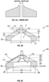
- FIG. 2A is a schematic diagram illustrating a cross section of a lower pole piece, in accordance with the current art.
- the lower pole piece does not typically include lateral apertures 175 as described in reference to FIG. 1E .
- lower pole piece of the current art typically include solid bodies that are rotationally symmetrical about a central aperture, aligned with the beam axis A of the TEM.
- lower pole piece of the current art incorporate additional apertures to serve as conduits of a vacuum system (as in environmental TEM systems) or to facilitate introduction of a beam aperture component, similar to the objective aperture, that is referred to as a "high contrast aperture.”
- a vacuum system as in environmental TEM systems
- a beam aperture component similar to the objective aperture
- the additional apertures are mechanically and fluidically coupled with vacuum systems, precluding the introduction of the optical cavity 140.
- the high contrast aperture can be used to enhance contrast in images of biological samples, the high contrast aperture is not inserted in a diffraction plane.
- FIG. 2B is a schematic diagram illustrating a cross section of an example lower pole piece 200, in accordance with some embodiments of the present disclosure.
- Example lower pole piece 200 is an example of lower pole piece 170 of FIG. 1E , which can be incorporated in example TEM system 100 of FIG. 1A .
- Example lower pole piece 200 includes multiple lateral apertures 205, disposed between an upper surface 210 and a lower surface 215 of a body 220.
- the example lower pole piece 200 further includes a central aperture 225, concentric with a central axis, B, about which the lateral apertures 205 are substantially symmetrically arrayed (e.g., rotationally symmetrical), as described in more detail in reference to FIGs. 3A-3D . As illustrated in FIG.
- the lateral apertures 205 are formed in the body 220 from a lateral surface 221 of the body 220 to the central aperture 225.
- the lateral surface 221 is inclined relative to the central axis B and tapers toward the upper surface 210.
- the lateral apertures 205 can be characterized by the vertical dimension 180.
- the vertical dimension 180 can vary with radial distance from the central axis B.
- the vertical dimension 180 is illustrated increasing with increasing distance from the central axis B.
- the vertical dimension 180 is substantially independent of radial distance from the central axis B.
- the vertical dimension 180 of the lateral aperture(s) 205 at the intersection with the central aperture 225 can overlap a range of positions of the diffraction plane 175, as described in more detail in reference to FIG. 3B , and FIG. 4 .
- the central aperture 225 is structured to integrate one or more components of the optical cavity 140 by including multiple sections, over which the central aperture 225 expands from a first width 230 at the upper surface 210 to a second width 231 at a position downstream of the upper surface 210 (e.g., at the lower surface 215).
- the central aperture 215 defines a first section 235 and a second section 240, with the central aperture 215 having a width substantially equal to the first width 230 in the first section 235 and an axially varying width, increasing from the first width 230 to the second width 231 at the lower surface 215. In this way, the central aperture 215 tapers toward the upper surface 210.
- the second width 231 can be from about 3 mm to about 50 mm, including sub-ranges, fractions, and interpolations thereof.
- the second width 231 can be about 3 mm, about 5 mm, about 10 mm, about 15 mm, about 20 mm, about 25 mm, about 30 mm, about 35 mm, about 40 mm, about 45 mm, or about 50 mm, including fractions and interpolations thereof.
- the second width 231 can be determined based at least in part on the magnetic saturation behavior of the lower pole piece 200 and the space used to house optical components and to keep the area around the beam of electrons 155 clear.
- the central aperture 215 is substantially symmetrical about the central axis B.
- the body 220 can be formed of a material that conducts magnetic fields (e.g., characterized by relatively high magnetic permeability), as an approach to using electromagnetic lenses in the objective section 120 of the TEM 100.
- FIG. 2C is a schematic diagram illustrating a cross section of an example lower pole piece 245 including a graduated central aperture 225, in accordance with some embodiments of the present disclosure.
- Example lower pole piece 245 includes four sections: the first section 235, the second section 240, a third section 241, and a fourth section 243. With increasing distance from the upper surface 210 toward the lower surface 215, the width of each progressive section increases, from the first width 230 to a second width 250 and then to a third width 255. It is noted that the geometries illustrated in FIG. 2C are not executed to scale and are provided to illustrate structural features of the central aperture 225.
- the third section 241 can define an intermediate surface 260, between the upper surface 210 and the lower surface 215 with respect to the central axis B.
- the intermediate surface 260 can include a groove, ridge, knife edge, or other surface feature 261 configured to form a vacuum tight seal with a corresponding component of the TEM system 100, such as a liner tube, flange adapter, or the like, for example, via a metal gasket or elastomeric o-ring.
- the flange adapter can be configured to interface at a first surface with the intermediate surface 260 and with the liner tube on a second surface.
- the example lower pole piece 245 can be configured to mechanically couple with the liner tube via the flange adapter.
- the second width 250 of the second section 240 can be substantially constant and can be wider than the first width 230 and narrower than the third width 255.
- the third width 255 can be from about 5 mm to about 100 mm, including sub-ranges, fractions, and interpolations thereof.
- the second width 231 can be about 5 mm, about 10 mm, about 15 mm, about 20 mm, about 25 mm, about 30 mm, about 35 mm, about 40 mm, about 45 mm, or about 50 mm, about 55 mm, or about 60 mm, about 65 mm, or about 70 mm, about 75 mm, about 80 mm, about 85 mm, about 90 mm, about 95 mm, about 100 mm, including fractions and interpolations thereof.
- the third width 255 can be determined based at least in part on structural constraints involved in forming a vacuum tight seal without deforming the lower pole piece 245, with larger widths being limited by the vertical space available in the objective section 120. For example, to reduce strain-deformation of the lower pole piece 245, a larger third width 255 can correspond to a larger third section 241, which can also influence the electromagnetic characteristics of the objective section 120 (e.g., objective lens performance).
- the fourth section 243 can taper toward the first section 235, having a width at the junction of the fourth section 243 and the second section 240 that can be less than or equal to the second width 250.
- the pole pieces 200 and 245 of FIGs. 2B-2C can be configured to include lateral apertures 205 that facilitate the introduction of the optical cavity 140 and the EM radiation 150 into the central aperture 225.
- the central aperture can incorporate components of the optical system used to align and/or operate the optical cavity 140 that occupy additional space and can remain in the lower pole piece 200 and 245 while the optical cavity 140 is absent. In this way, the size 141 and length 143 of the optical cavity 140 can be reduced relative to a system that incorporates alignment and calibration components in a retractable member that is extended into the central aperture 225 through a lateral aperture 205.
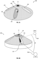
- FIG. 3A is a schematic diagram illustrating an example lower pole piece 300 including multiple lateral apertures 205, in accordance with some embodiments of the present disclosure.
- the example lower pole piece 300 is illustrated in partial section to focus description on the lateral surface 221 and the lateral apertures 205 formed through the body 220 from the lateral surface 221 to the central aperture 225.
- example lower pole piece 300 is an example of the lower pole piece 170 of FIG. 1E and the lower pole pieces 200 and 245 of FIGs. 2B-2C .
- four lateral apertures 205 are formed in the lateral surface 221 that are substantially symmetrical about the central axis B.
- a substantially symmetrical arrangement of the lateral apertures 205 about the central axis B is a functional consideration at least in part because the lateral apertures 205 are characterized by a different field permittivity than the body 220.
- an asymmetric arrangement can interfere with the operation of electromagnetic lenses used to form the beam of electrons 155, thereby introducing aberration, imaging artifacts, or decreased resolution in TEM imaging and microanalysis.
- rotational symmetry can induce aberrations, making the size, shape, and orientation of lateral apertures 205 functionally constrained by performance considerations.
- FIG. 3B is a schematic diagram illustrating the example lower pole piece 300 including lateral apertures 205 configured to optically couple electromagnetic radiation into the central aperture 225 of the pole piece 300, in accordance with some embodiments of the present disclosure.
- the example lower pole piece 300 can include lateral apertures 205 that are structured to optically couple one or more modalities of EM radiation (e.g., EM radiation 150 of FIG. 1E ) into the central aperture 225.
- EM radiation 150 of FIG. 1E e.g., EM radiation 150 of FIG. 1E
- the lateral aperture 205 is structured to couple first EM radiation 150-1 into and/or out of the central aperture 225 at one position of the lateral aperture 205 and is also structured to couple second EM radiation 150-2 into and/or out of the central aperture 225 at a second position of the lateral aperture 205.
- the first EM radiation 150-1 is characterized by a first diameter 305 and the second EM radiation 150-2 is characterized by a second diameter 310.
- the second diameter 310 is equal to or wider than the first diameter 305.
- first EM radiation 150-1 and second EM radiation 150-2 have substantially equal energy properties (e.g., central wavelength, energy distribution function, etc.).
- the optical cavity 140 can include a single-wavelength horizontal cavity in-coupled via second diameter 310, a single-wavelength tilted cavity in-coupled via first diameter 305, a single-wavelength multiple-mirror optical cavity 140 coupling EM radiation via first diameter 305 and second diameter 310.
- the lateral aperture 205 can taper toward the central aperture 225.
- the lateral aperture(s) 205 define a floor 315 and a ceiling 320, corresponding to regions of an inner surface of the lateral aperture(s) 205 that are proximal to the lower surface 215 and the upper surface 210, respectively.
- the floor 315 and/or the ceiling 320 can be or include curved surfaces. In this way, a line of the ceiling 320 nearest the upper surface 210 and a line of the floor 315 nearest the lower surface 215 can define an angle geometrically similar to angle ⁇ or an angle greater than angle ⁇ .
- the floor 315 is substantially normal to the central axis B, while the ceiling 320 slopes toward the central aperture 225. In some embodiments, both the ceiling 320 and the floor 315 taper toward the central aperture 225.
- FIG. 3C is a schematic diagram illustrating a cross section 325 of an example lateral aperture 205, in accordance with some embodiments of the present disclosure.
- the cross-section 325 defines a periphery 330 of the lateral aperture 205 that assumes a shape of a compound curve, where the floor 315 and the ceiling 320 are substantially circular segments that are joined by substantially straight segments.
- the lateral aperture 205 can include a region of empty space within the body 220 bridging two substantially cylindrical regions of empty space.
- the ceiling 320 corresponds to a portion of a substantially circular periphery with a first diameter 335.
- the ceiling 320 can be characterized by a first radius of curvature (e.g., half of the first diameter 335) from about 1 mm to about 10 mm, including sub-ranges, fractions, and interpolations thereof.
- the first radius of curvature can be about 1 mm, about 2 mm, about 3 mm, about 4 mm, about 5 mm, about 6 mm, about 7 mm, about 8 mm, about 9 mm, about 10 mm, or greater, including fractions or interpolations thereof.
- the first radius of curvature is substantially equal to the first diameter 305 or larger than the first diameter 305.
- the lateral aperture(s) 205 can be structured to couple first EM radiation 150-1 into and/or out of the central aperture 225 (e.g., via the optical cavity 140) while reducing the proportion of first EM radiation 150-1 that is absorbed or reflected by the body 220.
- the second radius of curvature can be from about 1 mm to about 3 mm in some embodiments, corresponding to a first diameter 335 from about 2 mm to about 6 mm.
- the floor 315 corresponds to a portion of a substantially circular periphery with a second diameter 340.
- the floor 315 can be characterized by a second radius of curvature (e.g., half of the second diameter 340) from about 1 mm to about 10 mm, including sub-ranges, fractions, and interpolations thereof.
- the second radius of curvature can be about 1 mm, about 2 mm, about 3 mm, about 4 mm, about 5 mm, about 6 mm, about 7 mm, about 8 mm, about 9 mm, about 10 mm, or greater, including fractions or interpolations thereof.
- the second radius of curvature is substantially equal to the second diameter 310 or larger than the second diameter 310.
- the lateral aperture(s) 205 can be structured to couple second EM radiation 150-2 into and/or out of the central aperture 225 (e.g., via the optical cavity 140 or via additional mirrors 145 as described in reference to FIG. 4B) while reducing the proportion of second EM radiation 150-2 that is absorbed or reflected by the body 220.
- the second radius of curvature can be from about 1 mm to about 5 mm in some embodiments, corresponding to a second diameter 340 from about 2 mm to about 10 mm.
- the vertical dimension 180 can be from about 5 mm to about 20 mm, including fractions, sub-ranges, and interpolations thereof.
- the lateral aperture(s) 205 are structured to accommodate the optical cavity 140 being introduced into the central aperture as part of the techniques described in reference to FIG. 1D .
- the lateral apertures(s) 205 can taper toward the central aperture 225, with the vertical dimension 180 increasing with increasing distance from the central aperture 225.
- the vertical dimension 180 at the intersection with the central aperture 225 is from about 5 mm, about 6 mm, about 7 mm, about 8 mm, about 9 mm, about 10 mm, about 11 mm, about 12 mm, about 13 mm, about 14 mm, about 15 mm, about 16 mm, about 17 mm, about 18 mm, about 19 mm, about 20 mm, or larger, including fractions and interpolations thereof.
- FIG. 3D is a schematic diagram illustrating the example lower pole piece 300 including lateral apertures 205 arranged substantially symmetrically about the central aperture 225, in accordance with some embodiments of the present disclosure.
- the example lower pole piece 300 includes two, three, four, five, six, or more apertures, arranged in a rotationally symmetric pattern about central axis B.
- an arrangement of four lateral apertures 205 can be characterized by a relative angle of 90 degrees between neighboring lateral apertures 205, and a relative angle of 180 degrees between opposing lateral apertures 205.
- neighboring lateral apertures 205 can be separated by a relative angle of 120 degrees, for five lateral apertures 205, a relative aperture of 72 degrees. In this way, the neighboring lateral apertures 205 can be determined from the ratio of 360 degrees and the number of lateral apertures 205. As with the symmetry of the arrangement of the lateral apertures 205, the number of lateral apertures 205 is a functional consideration, based at least in part on the impact of the lateral apertures on performance of electromagnetic lenses in the objective section of the TEM 100.
- using three lateral apertures 205 can reduce saturation of the electromagnetic field in the vicinity of the example lower pole piece 300, but can also introduce geometric considerations, such as providing for access to the central aperture from opposing sides, for example, to be used to outcouple EM radiation from the pole piece.
- FIG. 4 is a schematic diagram illustrating an optical cavity 140 disposed in the central aperture 225 of a lower pole piece 400 including lateral apertures 205, in accordance with some embodiments of the present disclosure.
- components of the optical cavity 140 such as a retention apparatus, alignment actuators, control electronics, or the like, are omitted to focus description on structural aspects of the lower pole piece 400.
- lateral apertures 205 are formed in the lower pole piece 400 to accommodate the alignment of the optical cavity 140 with the diffraction plane 165 formed by the beam of electrons 155 when operating under divergent illumination.
- the lateral aperture(s) can overlap a position on the central axis B corresponding to a vertical distance 405 from the upper surface 210 to the diffraction plane 165, from about 5 mm to about 20 mm, including sub-ranges, fractions, and interpolations thereof.
- the vertical distance 405 is about 5 mm, about 6 mm, about 7 mm, about 8 mm, about 9 mm, about 10 mm, about 11 mm, about 12 mm, about 13 mm, about 14 mm, about 15 mm, about 16 mm, about 17 mm, about 18 mm, about 19 mm, or about 20 mm, including fractions and interpolations thereof.
- a second vertical distance 410 describes the separation between the sample plane and the diffraction plane 165 under divergent illumination, as described in reference to FIG. 1E (e.g., from about 10 mm to about 30 mm). As such, the difference between the second distance 410 and the distance 405 can correspond to one half of the vertical spacing Z, as described in more detail in reference to FIG. 1B .
- EM radiation 150 such as a beam of photons
- EM radiation 150 corresponding to first EM radiation 150-1 of FIG. 3B
- EM radiation 150 is coupled into a first mirror 145-1 that is configured to transmit the EM radiation 150 in a forward direction and to reflect the EM radiation 150 in the reverse direction.
- EM radiation 150 coupled into the optical cavity is trapped in the optical cavity 140, notwithstanding various loss mechanisms attributable to material and physical properties of the mirrors 145 and mirror substrates.
- the optical cavity 140 can include a second mirror 145-2 that generate the optical conditions at the diffraction plane 165 that result in a phase shift of the electron beam (e.g., phase-shifted beam 162 of FIG. 1D ).
- the optical cavity 140 can include two or more mirrors 145.
- each mirror can have a respective radius of curvature that shapes the EM radiation 150 as an approach to reducing the size 141 and length 143 of the optical cavity.
- the diameter of the beam of EM radiation 150 at the second mirror 145-2 can be narrower, wider, or equal to the diameter of the beam of EM radiation 150 coupled into the first mirror 145-1.
- the first mirror 145-1 and the second mirror 145-2 can be oriented relative to the central axis B by an angle ⁇ .
- the angle ⁇ can be determined based at least in part on the angle that gives rise to a lattice fringe pattern that is oriented relative to the beam axis A by a given angle.
- the angular alignment of the lattice fringes and the angle ⁇ can be equal.
- the lateral aperture(s) 205 can taper toward the central aperture 225 at an angle, relative to a plane normal to the central axis B, substantially equal to or greater than the angle ⁇ . In some embodiments, the taper angle is less than the angle ⁇ , for example, where the vertical dimension 180 of the lateral aperture(s) 205 is large enough to accommodate the optical cavity 140 and incident EM radiation 150 without interference by the body 220. It is understood however, that constraints are imposed on the structure of the lateral apertures 205 by the threshold for magnetic saturation of the pole piece.
- FIG. 5 is a block flow diagram illustrating an example process 500 for improving phase contrast in electron microscope images, in accordance with some embodiments of the present disclosure.
- One or more operations of the example process 500 may be executed by a computer system in communication with additional systems including, but not limited to, characterization systems, network infrastructure, databases, and user interface devices.
- additional systems including, but not limited to, characterization systems, network infrastructure, databases, and user interface devices.
- at least a subset of the operations described in reference to FIG. 5 are performed automatically (e.g., without human involvement) or semi-automatically (e.g., with human initiation or limited human intervention).
- operations for generating and shaping the beam of electrons 155 can be executed automatically, with the TEM system 100 being configured to maintain properties of the beam of electrons 155 at or about a set point that can be designated by a human user.
- a human user can initiate phase-contrast imaging using the techniques described herein by activating a subsystem of the TEM 100 (e.g., through an interactive user environment presented through a user terminal, such as a browser or software application, and/or a push-button control panel) that automatically modifies the operation of the TEM 100 from parallel illumination mode to divergent illumination mode and automatically extends the optical cavity 140 into the central aperture 225 or bring the cavity that is already present in suitable operation conditions.
- example process 500 is described as a sequence of operations, it is understood that at least some of the operations can be omitted, repeated, and/or reordered. In some embodiments, additional operations precede and/or follow the operations of example process 500 that are omitted for clarity of explanation. For example, operations for calibration of the electron source, alignment and aberration correction of the beam of electrons 155, or the like.
- example process 500 includes introducing the optical cavity 140 into the central aperture 225 at operation 505, as described in more detail in reference to FIGs. 4A-4B.
- Introducing the optical cavity 140 can include one or more sub-processes, such as actuating an arm bearing the optical cavity 140, retention structure, alignment mechanisms, or the like, to move the optical cavity 140 into position in the central aperture 225.
- the position of the optical cavity 140 in the central aperture 225 corresponds to a vertical position on the central axis B of the diffraction plane 165, as described in more detail in reference to FIG. 1E .
- the retention structure, alignment mechanisms, or other components of the TEM system 100 can retain a pair of mirrors in a configuration that is aligned along an optical axis 157 angled relative to the central axis 225 by the angle ⁇ .
- Example process 500 can omit operation 505.
- the optical cavity 140 can be configured to maintain a clearance about the beam axis A, as where one or more components of the optical cavity 140 are disposed in the central aperture 225.
- mirrors 145 and/or a retention apparatus can be disposed in the central aperture 225, such that the optical cavity 140 can remain in the central aperture 225 over multiple iterations of example process 500, during operation of the TEM 100 in general, etc.
- the optical cavity 140 can already be present in the central aperture 225 prior to initiation of the example process 500.
- example process 500 includes generating a converging beam of electrons 155 at operation 510.
- the operation 510 can follow other operations for generating a diverging beam upstream of the sample plane, such that the sample is exposed under divergent illumination. In this way, force applied to the beam of electrons 155 to converge toward the diffraction plane can be applied downstream of the sample plane.
- the converging beam of electrons 155 is aligned with the beam axis A and converges toward the diffraction plane 165.
- the diffraction plane 165 intersects the central axis 225 at a position on the central axis 225 between the upper surface 210 and the lower surface 215 and is aligned with the plurality of lateral apertures 205.
- Generating the converging beam of electrons 155 can include applying an electromagnetic force to the beam of electrons 155 using one or more electromagnetic lenses 125 (e.g., condenser lens(es)) in the TEM column, resulting in shifting one of the central antinodes (or fringes) to a position in the central aperture 225 of a lower pole piece (e.g., example lower pole piece 200 of FIG. 2B , example lower pole piece 245 of FIG. 2C , example lower pole piece 300 of FIGs. 3A-3B , example lower pole piece 400 of FIG. 4A, or example lower pole piece 450 of FIG. 4B) in accordance with the converging beam of electrons being passed through the pole piece at operation 515.
- electromagnetic lenses 125 e.g.
- Some embodiments of the present disclosure include a system including one or more data processors and/or logic circuits.
- the system includes a non-transitory computer readable storage medium containing instructions which, when executed on the one or more data processors, cause the one or more data processors to perform part or all of one or more methods and/or part or all of one or more processes and workflows disclosed herein.
- Some embodiments of the present disclosure include a computer-program product tangibly embodied in a non-transitory machine-readable storage medium, including instructions configured to cause one or more data processors to perform part or all of one or more methods and/or part or all of one or more processes disclosed herein.
- the terms “about” or “substantially” are intended to reflect that the alignment or angular orientation can be different from the exact stated condition (e.g., not exactly normal) within a tolerable limit.
- the central axis B of the lower pole piece 200 can be "substantially aligned" with the beam of electrons 155, which can include a deviation from exact alignment resulting from physical phenomena affecting the direction of the beam of electrons 155 (e.g., beam drift).
- dimensional values such as diameters, lengths, widths, or the like
- the term “about” can be understood to describe a deviation from the stated value of up to ⁇ 10%.
- a dimension of "about 10 mm” can describe a dimension from 9 mm to 11 mm.
Landscapes
- Chemical & Material Sciences (AREA)
- Analytical Chemistry (AREA)
- Physics & Mathematics (AREA)
- Electromagnetism (AREA)
- Analysing Materials By The Use Of Radiation (AREA)
Abstract
Systems, methods, and components of charged particle microscopes affording improved contrast in dose sensitive samples are described. A pole piece for an electron microscope can include a body, being substantially concentric with a central axis. The body can define an upper surface, substantially normal to the central axis, a lower surface, substantially normal to the central axis, a central aperture formed in the body from the upper surface to the lower surface. The central aperture can be substantially rotationally symmetrical about the central axis. The body can define a lateral surface, inclined relative to the central axis and tapering toward the upper surface and a plurality of lateral apertures formed in the body from the lateral surface to the central aperture. The plurality of lateral apertures can be arrayed substantially symmetrically about the central axis.
Description
- Embodiments of the present disclosure are directed to electron microscopy components, systems, and methods. In particular, some embodiments are directed toward components configured for improved contrast in electron microscope images.
- Electron microscopy of biological samples involves exposure of organic materials to a beam of electrons. Interaction between electrons and the sample generates different types of detectable signals that can be used for imaging and analysis. In transmission electron microscopes (TEMs), detailed information can be developed at the atomic scale, including images of the internal structures of biological materials, conformational information, and in-situ observations of microbiological processes.
- TEM analysis of biological materials at progressively smaller length scales, such as those on the order of Angstroms to tens of Angstroms, introduces challenges in differentiating structures of interest from background signals or imaging artifacts. As such, there is a need to develop components, systems, and methods for improved contrast in electron microscope images, for example, in the field of cryogenic TEM analysis of biological materials.
Further aspects of the present disclosure as set forth in the following numbered clauses:- -
Clause 1. A microscope system, comprising:- a pole piece including a body, the body being substantially rotationally symmetrical about a central axis, wherein the body defines:
- an upper surface, substantially normal to the central axis;
- a lower surface, substantially normal to the central axis;
- a central aperture formed in the body from the upper surface to the lower surface, the central aperture being substantially rotationally symmetrical about the central axis;
- a lateral surface, inclined relative to the central axis and tapering toward the upper surface; and
- a plurality of lateral apertures formed in the body from the lateral surface to the central aperture, wherein the plurality of lateral apertures is arrayed substantially symmetrically about the central axis;
- an electron source configured to generate a beam of electrons substantially aligned with the central axis;
- a sample holder disposed in the microscope system at a first position on the central axis between the electron source and the pole piece; and
- one or more electromagnetic lenses configured to shape the beam of electrons such that the beam of electrons diverges away from the central axis at a second position on the central axis between the electron source and the sample holder.
- a pole piece including a body, the body being substantially rotationally symmetrical about a central axis, wherein the body defines:
- Clause 2. The microscope system of
clause 1, wherein the plurality of lateral apertures respectively intersect the central aperture at a vertical distance relative to the upper surface from about 5 mm to about 20 mm, corresponding to a first diffraction plane of the beam of electrons. - Clause 3. The microscope system of
clause 1, wherein a lateral aperture of the plurality of lateral apertures tapers toward the central aperture at an angle from about 10 degrees to about 45 degrees relative to a lateral reference plane normal to the central axis. - Clause 4. The microscope system of
clause 1, wherein:- a lateral aperture of the plurality of lateral apertures defines a floor and a ceiling;
- a cross section of the lateral aperture parallel with the central axis defines a compound curve connecting the floor and the ceiling;
- the ceiling is characterized by a first radius of curvature from about 1 mm to about 10 mm; and
- the floor is characterized by a second radius of curvature from about 1 mm to about 10 mm.
- Clause 5. The microscope system of clause 4, wherein the first radius of curvature is from about 1 mm to about 3 mm and wherein the second radius of curvature is from about 1 mm to about 5 mm.
- Clause 6. The microscope system of
clause 1, wherein the central aperture comprises a plurality of sections, wherein a first section of the plurality of sections is characterized by a diameter from about 1 mm to about 10 mm, wherein a second section of the plurality of sections is characterized by a diameter from about 5 mm to about 50 mm, and wherein the second section is wider than the first section. - Clause 7. The microscope system of clause 6, wherein a third section of the plurality of sections is characterized by a diameter from about 10 mm to about 30 mm, wherein the third section is wider than the second section, and wherein the second section is between the first section and the third section.
- The foregoing aspects and many of the attendant advantages of the present disclosure will become more readily appreciated as the same become better understood by reference to the following detailed description, when taken in conjunction with the accompanying drawings.
-
FIG. 1A is a schematic diagram illustrating a transmission electron microscope (TEM) system, in accordance with some embodiments of the present disclosure. -
FIG. 1B is a schematic diagram illustrating an objective section of a transmission electron microscope including components used for analysis of cryogenic samples, in accordance with some embodiments of the present disclosure. -
FIG. 1C is a schematic diagram illustrating interaction of electromagnetic radiation with a beam of electrons, in accordance with some embodiments of the present disclosure. -
FIG. 1D is a schematic diagram illustrating a sample under parallel illumination, in accordance with some embodiments of the present disclosure. -
FIG. 1E is a schematic diagram illustrating a sample under divergent illumination, in accordance with some embodiments of the present disclosure. -
FIG. 2A is a schematic diagram illustrating a cross section of a lower pole piece, in accordance with the current art. -
FIG. 2B is a schematic diagram illustrating a cross section of a lower pole piece, in accordance with some embodiments of the present disclosure. -
FIG. 2C is a schematic diagram illustrating a cross section of a lower pole piece including a graduated central aperture, in accordance with some embodiments of the present disclosure. -
FIG. 3A is a schematic diagram illustrating a lower pole piece including lateral apertures, in accordance with some embodiments of the present disclosure. -
FIG. 3B is a schematic diagram illustrating a lower pole piece including lateral apertures configured to optically couple electromagnetic radiation into the central aperture of the pole piece, in accordance with some embodiments of the present disclosure. -
FIG. 3C is a schematic diagram illustrating a cross section of a lateral aperture, in accordance with some embodiments of the present disclosure. -
FIG. 3D is a schematic diagram illustrating a lower pole piece including lateral apertures arranged substantially symmetrically about the central aperture, in accordance with some embodiments of the present disclosure. -
FIG. 4 is a schematic diagram illustrating an optical cavity disposed in the central aperture of a lower pole piece including lateral apertures, in accordance with some embodiments of the present disclosure. -
FIG. 5 is a block flow diagram illustrating an example process for improving phase contrast in electron microscope images, in accordance with some embodiments of the present disclosure. - In the drawings, like reference numerals refer to like parts throughout the various views unless otherwise specified. Not all instances of an element are necessarily labeled to reduce clutter in the drawings where appropriate. The drawings are not necessarily to scale, emphasis instead being placed upon illustrating the principles being described.
- While illustrative embodiments have been illustrated and described, it will be appreciated that various changes can be made therein without departing from the spirit and scope of the disclosure.
- In the forthcoming paragraphs, embodiments of an electron microscope system, components, and methods for improving contrast in electron microscope images are provided. Embodiments of the present disclosure include a transmission electron microscope incorporating a lower pole piece configured to receive, include, and/or incorporate an optical cavity or components of an optical cavity. The optical cavity can be configured to concentrate electromagnetic radiation onto a beam of electrons at a position substantially corresponding to a first diffraction plane of the beam of electrons. In some embodiments, the optical cavity can keep the area of the beam of electrons free of optical elements or other material. The lower pole piece can include a central aperture and multiple lateral apertures configured to accommodate the optical cavity and to permit EM radiation to be provided to the optical cavity from a radiation source external to the lower pole piece. As a result, imaging performance of TEM microscopes can be improved, for example, during imaging of biological samples.
- Electron microscopy of biological samples involves exposure of biomaterials to a beam of electrons. Interaction between electrons and the sample generates different types of detectable signals that can be used for imaging and analysis. In transmission electron microscopes (TEMs), detailed information can be developed at the atomic scale, including images of the internal structures of biological materials, conformations of biomolecules, and in-situ observations of microbiological processes. TEM analysis of biological materials at progressively smaller length scales, such as those on the order of ones to tens of Angstroms, introduces challenges in differentiating structures of interest from background signals or imaging artifacts, due at least in part on the relatively low proportion of electrons that are scattered by biological samples. For at least these reasons, there is a need to develop components, systems, and methods for improved contrast in electron microscope images, for example, in the field of cryogenic TEM analysis of biological materials that exhibit sensitivity to radiation dose and a characteristic low signal-to-noise quality.
- A similar technical challenge exists in the field of charged particle microscopy of microbiological samples. Typically, a biological sample (e.g., a protein particle, cell or cell fragment, viral particle, bacteria-derived materials, or the like) is prepared by freezing (e.g., liquid nitrogen temperatures) and subsequently being placed in a sample holder configured to maintain cryogenic conditions. Organic materials from which biological samples are typically composed scatter a relatively small fraction of incident electrons (e.g., as opposed to heavier elements like iron, gold, or the like). In consequence, background information is typically significant and limits contrast in TEM images of biological samples. Similarly, electron beam microanalysis that is routinely used in inorganic materials, such as crystal diffraction patterns (e.g., used to identify phase structures of semiconducting or metallic crystalline materials) is inhibited by relatively weak signal-to-background information. Approaches including, but not limited to, dark field TEM and Zernike Phase Contrast TEM modes can be used to reduce the relative proportion of background illumination and to increase the relative signal from scattered electrons in TEM images.
- In the field of optical microscopy, resolved images of microbiological samples, which scatter a relatively small proportion of incident photons, can be improved through the use of phase-contrast microscopy. An operative principle of phase-contrast microscopy is to differentiate between photons that have been scattered by a sample and photons that have passed through the sample without scattering. In this context, scattering refers to an interaction between a photon and an atom of the sample that results in a phase shift of scattered photons. Introduction of optical elements (e.g., condenser annulus, phase shift ring, and filter ring elements) allows a phase-contrast microscope to selectively phase shift and attenuate unscattered photons and to improve contrast in images of biological samples. In contrast to photon optics, analogous optical elements are unavailable for charged particle optics systems, such as in TEM. For at least this reason, creating a controlled phase shift to either the scattered portion of an electron wave or an unscattered portion of the electron wave presents a significant technical challenge that impairs imaging of dose-sensitive samples.
- Electromagnetic radiation can be used to manipulate the beam of electrons generated in the TEM. As described in more detail in reference to
FIG. 1C , stimulated Compton scattering can be induced in a beam of electrons by exposure to electromagnetic radiation (e.g., a continuous wave laser, a pulsed laser, x-rays, or the like). As a result of this exposure, the electron can undergo a phase shift. In an example embodiment, a continuous wave laser can be directed into a resonant optical cavity. This principle can be used to achieve phase-contrast TEM, but its application is limited, at least in part because the size of the optical cavity is constrained and because of the limited space available in proximity to the electron beam. - One approach to increase contrast of nanostructured materials composed principally of light elements is to defocus the beam of electrons prior to incidence with the sample and applying EM radiation to the beam of electrons of suitable intensity at a position of a diffraction plane, thereby stimulating Compton scattering. This mode of illumination is referred to in the forthcoming paragraphs as "divergent illumination," and described in reference to
FIG. 1E . Such techniques permit, for example, visualization and measurement of interlayer spacings in carbon nanotubes and organic crystals that include a regular structure. Under divergent illumination, a first diffraction plane of the electron beam occurs at a point part-way between an upper surface and a lower surface of a lower pole piece forming a part of the objective section of the TEM, as described in more detail in reference toFIG. 1B , which allows a focal area of high intensity EM radiation to be aligned with the diffraction plane of the beam of electrons within a central aperture of the lower pole piece, away from other components of the objective section (e.g., the sample holder, an objective aperture, a cryobox, and a cryoshield). - Integration of an optical cavity into a body of the lower pole piece presents significant technical challenges. For example, apertures formed in the body to facilitate moving optical components into or out of the central aperture of the lower pole piece can lower the threshold maximum ampere-turns of the lens coil at which magnetic saturation of the pole piece material occurs. In another example, the shape, position, and orientation of the apertures is constrained by the position of the first diffraction plane and the angle of the optical cavity relative to a central axis of the lower pole piece. In yet another example, the size of the central aperture of the lower pole piece, which can be constrained by the inclusion of electromechanical alignment components, can introduce issues with maintaining vacuum integrity of the objective section and a liner tube of the TEM. In this way, configuring the lower pole piece to accept an optical cavity implicates multiple structural modifications to the lower pole piece that would not be used for other applications, such as vacuum system integration.
-
FIG. 1A is a schematic diagram illustrating an example transmission electron microscope (TEM)system 100, in accordance with some embodiments of the present disclosure. In the following description, details of internal components and functions of theexample TEM system 100 are omitted for simplicity and to focus description on various components, as described in more detail in reference toFIGs. 1B-1E , configured as described in more detail in reference toFIGs. 2A-4 for augmenting contrast in TEM images, as described in more detail in reference toFIG. 5 . Theexample TEM system 100 includes an electron gun section, a TEM column including anobjective section 120, and an imaging section. The present disclosure focuses on theobjective section 120. In brief, the electron gun section includes electronics configured to energize an electron source, which can include a high-voltage field-emission source or other sources of emitted electrons, such that a beam of electrons is formed and conducted through a vacuum into the TEM column. - The TEM column includes components for beam forming, including
electromagnetic lenses 125 and multiple apertures to control properties of the beam of electrons. TEM column components include condenser lenses, objective lenses, projector lenses, among others, as well as corresponding apertures. The imaging section includes one or more types of detectors, sensors, screens, and/or optics configured to generate images, spectra, and other data for use in sample analysis. For example, the imaging section can include a scintillator screen, binoculars, scanning transmission electron microscopy (STEM) detector(s), camera(s), electron energy loss spectroscopy (EELS) detectors, among others. -
FIG. 1B is a schematic diagram illustrating an exampleobjective section 120 of a transmission electron microscope including components used for analysis of cryogenic samples, in accordance with some embodiments of the present disclosure.FIG. 1B omits some elements of the objective section illustrated inFIG. 1A , such as the vacuum enclosure, to focus description on components of theTEM 100 that interact with a beam of electrons. The exampleobjective section 120 includes an upper pole piece, and a lower pole piece, a sample holder, and an objective aperture. In some cases, the objective section also includes components for use in imaging and/or analysis of cryogenic samples, such as a cryoshield. Similarly, theTEM 100 can be configured for automated serial analysis of multiple samples by including an automated sample loader. - In the context of the present disclosure, the volume available for integrating an optical cavity between the upper pole piece and the lower pole piece is limited by a lateral dimension "R" and a vertical dimension "Z," where "lateral" refers to a direction substantially normal to the beam axis, A, and "vertical" refers to a direction substantially parallel to the beam axis A. The term "substantially" is used to indicate that deviation in the angle between laterally oriented or vertically oriented components relative to the beam axis, A, can occur within the scope of the present disclosure.
- For improved contrast, one possible approach is to introduce the optical cavity between the lower pole piece and the sample holder. Where optical components and/or retention apparatus are present between the lower pole piece and the sample holder, dimensions R and Z define the available volume between upper pole piece and lower pole piece for introduction of an optical cavity. The vertical dimension Z can be from about 3 mm to about 25 mm, with different vertical dimensions being used for different types of analysis. The lateral dimension R can be from about 10 mm to about 15 mm, although in some cases optical components and/or retention components can be disposed outside of the volume at the cost of increased complexity of the optical system. In some systems, the sample holder is substantially centered with respect to the vertical dimension Z. As such, the vertical space available for an optical cavity, between the sample holder and the lower pole piece, can be from about 2 mm to about 4 mm. Horizontal space reserved for the electron beam implicates a lateral distance of 1 mm - 5 mm in the R dimension to be kept free of optical components. For cryo-TEM applications, space constraints are greater, with space in the vertical dimension Z being limited to 1.5 mm or less (e.g., in some cases, no space is available). In this way, space limitations prevent the use of the optical cavity between the sample holder and the lower pole piece. Alternatively, the optical cavity can be introduced into the lower pole itself, as described in more detail in reference to
FIGs. 1E - 4 . -
FIG. 1C is a schematic diagram illustrating an exampleoptical cavity 140, in accordance with some embodiments of the present disclosure. In some embodiments, the exampleoptical cavity 140 is configured to be integrated into a lower pole piece of an electron microscope, such as theTEM 100 ofFIG. 1 . In some embodiments, interaction of electromagnetic (EM)radiation 150 with a beam ofelectrons 155 is induced by passing the beam ofelectrons 155 through a focal area ofEM radiation 150 that is recirculated in theoptical cavity 140. To that end, theoptical cavity 140 can include two ormore mirrors 145 that together form a concentric-spherical cavity, a near-concentric cavity, a confocal cavity, a planar cavity, a near-planar cavity, or other configurations. Theoptical cavity 140 can be configured to concentrate EM radiation at the position of the beam of electrons 155 (e.g., at the position of the beam axis A). For example, constructive interference in theoptical cavity 140 can be induced by aligning themirrors 145 and setting alateral distance 143 such that a focal area ofEM radiation 150 intensity occurs substantially at the position of the beam ofelectrons 155. In an illustrative example, a 10 W laser can be introduced to theoptical cavity 140, where it can be concentrated in a focal area about the beam axis A at a power of about 100 kW. - In some embodiments, the
EM radiation 150 can include photons in the ultraviolet, visible, and/or infrared ranges. TheEM radiation 150 can be provided to theoptical cavity 140 as a beam of laser energy. For example, theEM radiation 150 can be a continuous wave laser, illustrated as a sinusoidal power signal. In an illustrative example, theEM radiation 150 can be generated in a Nd:YAG laser source or a CO2 laser source, configured to emit photons at a wavelength of 1064 nm. In another example, theEM radiation 150 can include frequency-doubled photons at 532 nm. - As described in reference to
FIG. 1B , maintaining space for the beam ofelectrons 155 to pass unimpeded through theoptical cavity 140 can impose functional constraints on the structure, spacing, and orientation of themirrors 145. Thesize 141 of theoptical cavity 140 in the vertical Z dimension and thelength 143 of theoptical cavity 140 in the lateral R dimension includes themirrors 145, the spacing between themirrors 145, and the retention apparatus used to hold themirrors 145 in place. In this way, the size of theoptical cavity 140 can be compared to the space between the sample holder and the lower pole piece to determine whether theoptical cavity 140 can be introduced external to the lower pole piece. Additionally, the cryo-box and the cryo-shield are also placed in the same area, further reducing the space available. - For a typical TEM system (e.g.,
TEM 100 ofFIG. 1A ) the distance between the sample holder and the lower pole piece can be from about 5 mm to about 11 mm, of which components of the sample stage, the objective aperture, and the components for cryo-microscopy can occupy as much as about 3 mm to about 4 mm below the sample plane. For theoptical cavity 140 to be stable and to keep the area around the beam ofelectrons 155 free of optical components, themirrors 145 can be from about 2 mm to about 10 mm in width (e.g., diameter). Including the retention apparatus can increase the vertical size of the optical cavity by as much as 10 mm or more. By comparing thesize 141 to the available space, it can be seen that theoptical cavity 140 is too large to be introduced between the sample holder and the lower pole piece. - Based at least in part on optical considerations, the
optical cavity 140 can define anoptical axis 157 that is oriented at an angle, α, relative to the beam ofelectrons 155, from about 45 degrees to about 90 degrees, including sub-ranges, fractions, and interpolations thereof. Orienting theoptical cavity 140 at the angle α can reduce the modulation effect of the standing wave pattern on the phase shift. In this way, phase shift can be exhibit negligible or no sensitivity to the position alongaxis 157 where the electron transits theEM wave 150. In some embodiments, a standing wave lattice arising betweenmirrors 145 is characterized by a central axis that is not aligned with theoptical axis 157. In some cases, α can be determined based at least in part on the angle between the beam axis A and the central axis of the lattice. In some embodiments, α can be an angle of about 45 degrees, about 50 degrees, about 55 degrees, about 60 degrees, about 65 degrees, about 70 degrees, about 75 degrees, about 80 degrees, about 85 degrees, or about 90 degrees, including fractions and interpolations thereof. Based at least in part on geometric considerations, performance of theoptical cavity 140 can be impaired by an angle α above 50 degrees. To that end, above about 40 degrees, thelength 143 of theoptical cavity 140 used to maintain the area of the beam ofelectrons 155 clear of optical components can be impracticable, making thesize 141 of theoptical cavity 140 greater than the space available for theoptical cavity 140 or at the cost of a smaller numerical aperture of theoptical cavity 140. Additionally or alternatively, energy transfer into theoptical cavity 140, for example, whereEM radiation 150 is introduced into theoptical cavity 140 via one or more of themirrors 145, can be impaired at relatively high angles, at least in part due to challenges associated with coupling the EM radiation 150 (e.g., a laser beam) into the objective section at the appropriate point and angle. - Advantageously, introducing the
optical cavity 140 into the path of the beam ofelectrons 155 can improve contrast in TEM images of biological samples or other samples that are sensitive to radiation dosage. Without being bound to a particular physical phenomenon or mechanism, the beam ofelectrons 155 can include a scattered portion and an un-scattered portion, where the scattered portion has collided with the sample (e.g., elastic interactions and/or inelastic interactions) and the un-scattered portion has transited the sample without colliding. Examples of interactions include absorption, reflection, deflection, ionization, or the like, that register as deviations from the background in TEM images. For example, in bright field TEM, a region of the sample that scattered electrons can appear darker than regions of the sample that did not scatter electrons. In this way, a sample that is characterized a generally low probability of scattering can include a relatively high proportion of un-scattered electrons and a relatively low proportion of scattered electrons, resulting in poor image contrast. - The interaction with the
EM radiation 150 in theoptical cavity 140 can result in a phase shift of the unscattered part of theelectron wave 155 that is passing the EM radiation 150 (e.g., inducing a phase shift from about 0 rad to about π/2 rad), which can generate a phase-contrast enhancement of the electron microscope image. -
FIG. 1D is a schematic diagram illustrating a sample under parallel illumination, in accordance with some embodiments of the present disclosure. In this context, parallel illumination refers to a technique of image generation in a TEM, such as theexample TEM 100 ofFIG. 1 , where a substantially parallel beam of electrons passes through the sample plane. Regions of the sample that absorb, reflect, and/or scatter electrons usually appear dark in images and other regions appear bright and electromagnetic lenses shape the beam such that an image can be projected onto a detector surface in the imaging section of the TEM. InFIGs. 1D-1E , electromagnetic lenses are illustrated as solid optical lenses, but it is understood that electromagnetic lenses act on charged particles through the imposition of electromagnetic fields, rather than through refraction as in photon optics. - In parallel illumination, a back focal plane and a first diffraction plane coincide between the lower pole piece and the sample plane. To incorporate contrast enhancement using EM radiation described in reference to
FIG. 1C , theoptical cavity 140 can be positioned at the back focal plane. As described in more detail in reference toFIG. 1B , however, the space available for theoptical cavity 140 is typically occupied by components of the sample holder or loader, an objective aperture, and/or a cryo-shield, among other elements of theobjective section 120. To that end, constraints on the size of theoptical cavity 140 make the introduction of optical components a significant structural challenge. -
FIG. 1E is a schematic diagram illustrating a sample under divergent illumination, in accordance with some embodiments of the present disclosure. In some embodiments, the structural constraints are addressed by operating the TEM under divergent illumination. In this context, divergent illumination refers to a focusing of the beam ofelectrons 155 upstream of the sample plane such that the sample is illuminated by an expanding beam. As shown, the objective lens acts to concentrate the beam ofelectrons 155, with one or more of the central antinodes in a standing wave occurring on adiffraction plane 165 partway between anupper surface 167 and alower surface 169 of alower pole piece 170. In this way, one or morelateral apertures 175 can be formed in thelower pole piece 170 to accommodate theoptical cavity 140. The position of thediffraction plane 165 can vary, based at least in part on the strength of the condenser lens or other operating parameters of theTEM 100. To that end, thediffraction plane 165 can form at a position on the beam axis A, relative to the sample plane, from about 10 mm to about 30 mm, including sub-ranges, fractions, and interpolations thereof. For example, thediffraction plane 165 can form at a position on the beam axis A, relative to the sample plane, of about 10 mm, about 11 mm, about 12 mm, about 13 mm, about 14 mm, about 15 mm, about 16 mm, about 17 mm, about 18 mm, about 19 mm, about 20 mm, about 21 mm, about 22 mm, about 23 mm, about 24 mm, about 25 mm, about 26 mm, about 27 mm, about 28 mm, about 29 mm, or about 30 mm, including fractions and interpolations thereof. - To facilitate insertion of the
optical cavity 140 at thediffraction plane 165, avertical dimension 180 of thelateral apertures 175 can overlap with thediffraction plane 165. As described in more detail in the forthcoming paragraphs, aspects of thelower pole piece 170 are structured to introduce theoptical cavity 140 such that a central antinode of theoptical cavity 140 substantially coincides with thediffraction plane 165 of the beam ofelectrons 155 under divergent illumination. In some cases, operating under divergent illumination can affect some aspects of optical performance. That being said, the effects, such as non-isotropic magnification, image distortion, and off-axis coma can be addressed with software correction of images or they can be ignored if they do not impact the image quality. -
FIG. 2A is a schematic diagram illustrating a cross section of a lower pole piece, in accordance with the current art. In TEM systems of the current art, the lower pole piece does not typically includelateral apertures 175 as described in reference toFIG. 1E . Instead, lower pole piece of the current art typically include solid bodies that are rotationally symmetrical about a central aperture, aligned with the beam axis A of the TEM. In some TEM systems, lower pole piece of the current art incorporate additional apertures to serve as conduits of a vacuum system (as in environmental TEM systems) or to facilitate introduction of a beam aperture component, similar to the objective aperture, that is referred to as a "high contrast aperture." In the context of vacuum conduits, couplings with vacuum components and orientation and/or location of the additional apertures do not facilitate the introduction of theoptical cavity 140 at thediffraction plane 165. For example, the additional apertures are mechanically and fluidically coupled with vacuum systems, precluding the introduction of theoptical cavity 140. Similarly, while the high contrast aperture can be used to enhance contrast in images of biological samples, the high contrast aperture is not inserted in a diffraction plane. -
FIG. 2B is a schematic diagram illustrating a cross section of an examplelower pole piece 200, in accordance with some embodiments of the present disclosure. Examplelower pole piece 200 is an example oflower pole piece 170 ofFIG. 1E , which can be incorporated inexample TEM system 100 ofFIG. 1A . Examplelower pole piece 200 includes multiplelateral apertures 205, disposed between anupper surface 210 and alower surface 215 of abody 220. The examplelower pole piece 200 further includes acentral aperture 225, concentric with a central axis, B, about which thelateral apertures 205 are substantially symmetrically arrayed (e.g., rotationally symmetrical), as described in more detail in reference toFIGs. 3A-3D . As illustrated inFIG. 2B , thelateral apertures 205 are formed in thebody 220 from alateral surface 221 of thebody 220 to thecentral aperture 225. Thelateral surface 221 is inclined relative to the central axis B and tapers toward theupper surface 210. - In this way, the
lateral apertures 205 can be characterized by thevertical dimension 180. As illustrated inFIG. 2B , thevertical dimension 180 can vary with radial distance from the central axis B. For example, thevertical dimension 180 is illustrated increasing with increasing distance from the central axis B. In some embodiments, thevertical dimension 180 is substantially independent of radial distance from the central axis B. To facilitate optical coupling ofEM radiation 150 into thecentral aperture 225 at the position of thediffraction plane 175 thevertical dimension 180 of the lateral aperture(s) 205 at the intersection with thecentral aperture 225 can overlap a range of positions of thediffraction plane 175, as described in more detail in reference toFIG. 3B , andFIG. 4 . - In some embodiments, the
central aperture 225 is structured to integrate one or more components of theoptical cavity 140 by including multiple sections, over which thecentral aperture 225 expands from afirst width 230 at theupper surface 210 to asecond width 231 at a position downstream of the upper surface 210 (e.g., at the lower surface 215). In the examplelower pole piece 200 illustrated inFIG. 2B , thecentral aperture 215 defines afirst section 235 and asecond section 240, with thecentral aperture 215 having a width substantially equal to thefirst width 230 in thefirst section 235 and an axially varying width, increasing from thefirst width 230 to thesecond width 231 at thelower surface 215. In this way, thecentral aperture 215 tapers toward theupper surface 210. Thesecond width 231 can be from about 3 mm to about 50 mm, including sub-ranges, fractions, and interpolations thereof. For example, thesecond width 231 can be about 3 mm, about 5 mm, about 10 mm, about 15 mm, about 20 mm, about 25 mm, about 30 mm, about 35 mm, about 40 mm, about 45 mm, or about 50 mm, including fractions and interpolations thereof. Thesecond width 231 can be determined based at least in part on the magnetic saturation behavior of thelower pole piece 200 and the space used to house optical components and to keep the area around the beam ofelectrons 155 clear. - In some embodiments, the
central aperture 215 is substantially symmetrical about the central axis B. Thebody 220 can be formed of a material that conducts magnetic fields (e.g., characterized by relatively high magnetic permeability), as an approach to using electromagnetic lenses in theobjective section 120 of theTEM 100. -
FIG. 2C is a schematic diagram illustrating a cross section of an examplelower pole piece 245 including a graduatedcentral aperture 225, in accordance with some embodiments of the present disclosure. Examplelower pole piece 245 includes four sections: thefirst section 235, thesecond section 240, a third section 241, and afourth section 243. With increasing distance from theupper surface 210 toward thelower surface 215, the width of each progressive section increases, from thefirst width 230 to asecond width 250 and then to athird width 255. It is noted that the geometries illustrated inFIG. 2C are not executed to scale and are provided to illustrate structural features of thecentral aperture 225. To that end, the third section 241 can define anintermediate surface 260, between theupper surface 210 and thelower surface 215 with respect to the central axis B. In some embodiments, theintermediate surface 260 can include a groove, ridge, knife edge, or other surface feature 261 configured to form a vacuum tight seal with a corresponding component of theTEM system 100, such as a liner tube, flange adapter, or the like, for example, via a metal gasket or elastomeric o-ring. The flange adapter can be configured to interface at a first surface with theintermediate surface 260 and with the liner tube on a second surface. To that end, the examplelower pole piece 245 can be configured to mechanically couple with the liner tube via the flange adapter. - In some embodiments, the
second width 250 of thesecond section 240 can be substantially constant and can be wider than thefirst width 230 and narrower than thethird width 255. Thethird width 255 can be from about 5 mm to about 100 mm, including sub-ranges, fractions, and interpolations thereof. For example, thesecond width 231 can be about 5 mm, about 10 mm, about 15 mm, about 20 mm, about 25 mm, about 30 mm, about 35 mm, about 40 mm, about 45 mm, or about 50 mm, about 55 mm, or about 60 mm, about 65 mm, or about 70 mm, about 75 mm, about 80 mm, about 85 mm, about 90 mm, about 95 mm, about 100 mm, including fractions and interpolations thereof. Thethird width 255 can be determined based at least in part on structural constraints involved in forming a vacuum tight seal without deforming thelower pole piece 245, with larger widths being limited by the vertical space available in theobjective section 120. For example, to reduce strain-deformation of thelower pole piece 245, a largerthird width 255 can correspond to a larger third section 241, which can also influence the electromagnetic characteristics of the objective section 120 (e.g., objective lens performance). - In some embodiments, the
fourth section 243 can taper toward thefirst section 235, having a width at the junction of thefourth section 243 and thesecond section 240 that can be less than or equal to thesecond width 250. In this way, thepole pieces FIGs. 2B-2C can be configured to includelateral apertures 205 that facilitate the introduction of theoptical cavity 140 and theEM radiation 150 into thecentral aperture 225. Further, the central aperture can incorporate components of the optical system used to align and/or operate theoptical cavity 140 that occupy additional space and can remain in thelower pole piece optical cavity 140 is absent. In this way, thesize 141 andlength 143 of theoptical cavity 140 can be reduced relative to a system that incorporates alignment and calibration components in a retractable member that is extended into thecentral aperture 225 through alateral aperture 205. -
FIG. 3A is a schematic diagram illustrating an examplelower pole piece 300 including multiplelateral apertures 205, in accordance with some embodiments of the present disclosure. The examplelower pole piece 300 is illustrated in partial section to focus description on thelateral surface 221 and thelateral apertures 205 formed through thebody 220 from thelateral surface 221 to thecentral aperture 225. In this way, examplelower pole piece 300 is an example of thelower pole piece 170 ofFIG. 1E and thelower pole pieces FIGs. 2B-2C . In the illustrated embodiment of examplelower pole piece 300, fourlateral apertures 205 are formed in thelateral surface 221 that are substantially symmetrical about the central axis B. In the context of the present disclosure, a substantially symmetrical arrangement of thelateral apertures 205 about the central axis B is a functional consideration at least in part because thelateral apertures 205 are characterized by a different field permittivity than thebody 220. In this way, an asymmetric arrangement can interfere with the operation of electromagnetic lenses used to form the beam ofelectrons 155, thereby introducing aberration, imaging artifacts, or decreased resolution in TEM imaging and microanalysis. Conversely, rotational symmetry can induce aberrations, making the size, shape, and orientation oflateral apertures 205 functionally constrained by performance considerations. -
FIG. 3B is a schematic diagram illustrating the examplelower pole piece 300 includinglateral apertures 205 configured to optically couple electromagnetic radiation into thecentral aperture 225 of thepole piece 300, in accordance with some embodiments of the present disclosure. The examplelower pole piece 300 can includelateral apertures 205 that are structured to optically couple one or more modalities of EM radiation (e.g.,EM radiation 150 ofFIG. 1E ) into thecentral aperture 225. In the illustrated embodiment ofFIG. 3B , thelateral aperture 205 is structured to couple first EM radiation 150-1 into and/or out of thecentral aperture 225 at one position of thelateral aperture 205 and is also structured to couple second EM radiation 150-2 into and/or out of thecentral aperture 225 at a second position of thelateral aperture 205. The first EM radiation 150-1 is characterized by afirst diameter 305 and the second EM radiation 150-2 is characterized by asecond diameter 310. In some embodiments, thesecond diameter 310 is equal to or wider than thefirst diameter 305. In this context, the term "diameter" is used to describe a beam having a "width" attributed to a position at which power, flux, or the like, is below a threshold value (e.g., Rayleigh beamwidth, full width at half maximum, etc.). In some embodiments, first EM radiation 150-1 and second EM radiation 150-2 have substantially equal energy properties (e.g., central wavelength, energy distribution function, etc.). For example, theoptical cavity 140 can include a single-wavelength horizontal cavity in-coupled viasecond diameter 310, a single-wavelength tilted cavity in-coupled viafirst diameter 305, a single-wavelength multiple-mirroroptical cavity 140 coupling EM radiation viafirst diameter 305 andsecond diameter 310. - As described in more detail in reference to FIG. 4B, the
lateral aperture 205 can taper toward thecentral aperture 225. In some embodiments, the lateral aperture(s) 205 define afloor 315 and aceiling 320, corresponding to regions of an inner surface of the lateral aperture(s) 205 that are proximal to thelower surface 215 and theupper surface 210, respectively. As described in more detail in reference toFIG. 3C , thefloor 315 and/or theceiling 320 can be or include curved surfaces. In this way, a line of theceiling 320 nearest theupper surface 210 and a line of thefloor 315 nearest thelower surface 215 can define an angle geometrically similar to angle β or an angle greater than angle β. In some embodiments, thefloor 315 is substantially normal to the central axis B, while theceiling 320 slopes toward thecentral aperture 225. In some embodiments, both theceiling 320 and thefloor 315 taper toward thecentral aperture 225. -
FIG. 3C is a schematic diagram illustrating across section 325 of anexample lateral aperture 205, in accordance with some embodiments of the present disclosure. In some embodiments, thecross-section 325 defines aperiphery 330 of thelateral aperture 205 that assumes a shape of a compound curve, where thefloor 315 and theceiling 320 are substantially circular segments that are joined by substantially straight segments. In this way, thelateral aperture 205 can include a region of empty space within thebody 220 bridging two substantially cylindrical regions of empty space. In some embodiments, theceiling 320 corresponds to a portion of a substantially circular periphery with afirst diameter 335. As such, theceiling 320 can be characterized by a first radius of curvature (e.g., half of the first diameter 335) from about 1 mm to about 10 mm, including sub-ranges, fractions, and interpolations thereof. For example, the first radius of curvature can be about 1 mm, about 2 mm, about 3 mm, about 4 mm, about 5 mm, about 6 mm, about 7 mm, about 8 mm, about 9 mm, about 10 mm, or greater, including fractions or interpolations thereof. In some embodiments, the first radius of curvature is substantially equal to thefirst diameter 305 or larger than thefirst diameter 305. As such, the lateral aperture(s) 205 can be structured to couple first EM radiation 150-1 into and/or out of the central aperture 225 (e.g., via the optical cavity 140) while reducing the proportion of first EM radiation 150-1 that is absorbed or reflected by thebody 220. As an example of a sub-range, the second radius of curvature can be from about 1 mm to about 3 mm in some embodiments, corresponding to afirst diameter 335 from about 2 mm to about 6 mm. - In some embodiments, the
floor 315 corresponds to a portion of a substantially circular periphery with asecond diameter 340. As such, thefloor 315 can be characterized by a second radius of curvature (e.g., half of the second diameter 340) from about 1 mm to about 10 mm, including sub-ranges, fractions, and interpolations thereof. As with the first radius of curvature, the second radius of curvature can be about 1 mm, about 2 mm, about 3 mm, about 4 mm, about 5 mm, about 6 mm, about 7 mm, about 8 mm, about 9 mm, about 10 mm, or greater, including fractions or interpolations thereof. In some embodiments, the second radius of curvature is substantially equal to thesecond diameter 310 or larger than thesecond diameter 310. As such, the lateral aperture(s) 205 can be structured to couple second EM radiation 150-2 into and/or out of the central aperture 225 (e.g., via theoptical cavity 140 or viaadditional mirrors 145 as described in reference to FIG. 4B) while reducing the proportion of second EM radiation 150-2 that is absorbed or reflected by thebody 220. As an example of a sub-range, the second radius of curvature can be from about 1 mm to about 5 mm in some embodiments, corresponding to asecond diameter 340 from about 2 mm to about 10 mm. - The
vertical dimension 180 can be from about 5 mm to about 20 mm, including fractions, sub-ranges, and interpolations thereof. As described in more detail in reference toFIG. 1E , the lateral aperture(s) 205 are structured to accommodate theoptical cavity 140 being introduced into the central aperture as part of the techniques described in reference toFIG. 1D . To that end, the lateral apertures(s) 205 can taper toward thecentral aperture 225, with thevertical dimension 180 increasing with increasing distance from thecentral aperture 225. In some embodiments, thevertical dimension 180 at the intersection with thecentral aperture 225 is from about 5 mm, about 6 mm, about 7 mm, about 8 mm, about 9 mm, about 10 mm, about 11 mm, about 12 mm, about 13 mm, about 14 mm, about 15 mm, about 16 mm, about 17 mm, about 18 mm, about 19 mm, about 20 mm, or larger, including fractions and interpolations thereof. -
FIG. 3D is a schematic diagram illustrating the examplelower pole piece 300 includinglateral apertures 205 arranged substantially symmetrically about thecentral aperture 225, in accordance with some embodiments of the present disclosure. In some embodiments, the examplelower pole piece 300 includes two, three, four, five, six, or more apertures, arranged in a rotationally symmetric pattern about central axis B. For example, an arrangement of fourlateral apertures 205 can be characterized by a relative angle of 90 degrees between neighboringlateral apertures 205, and a relative angle of 180 degrees between opposinglateral apertures 205. Similarly, for three lateral apertures, neighboringlateral apertures 205 can be separated by a relative angle of 120 degrees, for fivelateral apertures 205, a relative aperture of 72 degrees. In this way, the neighboringlateral apertures 205 can be determined from the ratio of 360 degrees and the number oflateral apertures 205. As with the symmetry of the arrangement of thelateral apertures 205, the number oflateral apertures 205 is a functional consideration, based at least in part on the impact of the lateral apertures on performance of electromagnetic lenses in the objective section of theTEM 100. For example, using threelateral apertures 205 can reduce saturation of the electromagnetic field in the vicinity of the examplelower pole piece 300, but can also introduce geometric considerations, such as providing for access to the central aperture from opposing sides, for example, to be used to outcouple EM radiation from the pole piece. -
FIG. 4 is a schematic diagram illustrating anoptical cavity 140 disposed in thecentral aperture 225 of alower pole piece 400 includinglateral apertures 205, in accordance with some embodiments of the present disclosure. In the diagram, components of theoptical cavity 140, such as a retention apparatus, alignment actuators, control electronics, or the like, are omitted to focus description on structural aspects of thelower pole piece 400. For example,lateral apertures 205 are formed in thelower pole piece 400 to accommodate the alignment of theoptical cavity 140 with thediffraction plane 165 formed by the beam ofelectrons 155 when operating under divergent illumination. To that end, the lateral aperture(s) can overlap a position on the central axis B corresponding to avertical distance 405 from theupper surface 210 to thediffraction plane 165, from about 5 mm to about 20 mm, including sub-ranges, fractions, and interpolations thereof. In some embodiments, thevertical distance 405 is about 5 mm, about 6 mm, about 7 mm, about 8 mm, about 9 mm, about 10 mm, about 11 mm, about 12 mm, about 13 mm, about 14 mm, about 15 mm, about 16 mm, about 17 mm, about 18 mm, about 19 mm, or about 20 mm, including fractions and interpolations thereof. A secondvertical distance 410 describes the separation between the sample plane and thediffraction plane 165 under divergent illumination, as described in reference toFIG. 1E (e.g., from about 10 mm to about 30 mm). As such, the difference between thesecond distance 410 and thedistance 405 can correspond to one half of the vertical spacing Z, as described in more detail in reference toFIG. 1B . -
EM radiation 150, such as a beam of photons, can be coupled into theoptical cavity 140 via one or more mirrors 145. In the illustrated embodiment,EM radiation 150, corresponding to first EM radiation 150-1 ofFIG. 3B , is coupled into a first mirror 145-1 that is configured to transmit theEM radiation 150 in a forward direction and to reflect theEM radiation 150 in the reverse direction. In this way,EM radiation 150 coupled into the optical cavity is trapped in theoptical cavity 140, notwithstanding various loss mechanisms attributable to material and physical properties of themirrors 145 and mirror substrates. Theoptical cavity 140 can include a second mirror 145-2 that generate the optical conditions at thediffraction plane 165 that result in a phase shift of the electron beam (e.g., phase-shifted beam 162 ofFIG. 1D ). To that end, theoptical cavity 140 can include two or more mirrors 145. In another example, each mirror can have a respective radius of curvature that shapes theEM radiation 150 as an approach to reducing thesize 141 andlength 143 of the optical cavity. The diameter of the beam ofEM radiation 150 at the second mirror 145-2 can be narrower, wider, or equal to the diameter of the beam ofEM radiation 150 coupled into the first mirror 145-1. - As described in more detail in reference to
FIG. 1C , the first mirror 145-1 and the second mirror 145-2 can be oriented relative to the central axis B by an angle α. As described in more detail in reference toFIG. 1C , the angle α can be determined based at least in part on the angle that gives rise to a lattice fringe pattern that is oriented relative to the beam axis A by a given angle. In some embodiments, for example, where mirrors are configured to generate the lattice fringe pattern that is substantially centered between the mirrors and aligned substantially normal to theoptical axis 157, the angular alignment of the lattice fringes and the angle α can be equal. - To facilitate
coupling EM radiation 150 into the first mirror 145-1, or to accommodate the first mirror 145-1 and/or the other elements of theoptical cavity 140 into thecentral aperture 225, the lateral aperture(s) 205 can taper toward thecentral aperture 225 at an angle, relative to a plane normal to the central axis B, substantially equal to or greater than the angle β. In some embodiments, the taper angle is less than the angle β, for example, where thevertical dimension 180 of the lateral aperture(s) 205 is large enough to accommodate theoptical cavity 140 andincident EM radiation 150 without interference by thebody 220. It is understood however, that constraints are imposed on the structure of thelateral apertures 205 by the threshold for magnetic saturation of the pole piece. -
FIG. 5 is a block flow diagram illustrating anexample process 500 for improving phase contrast in electron microscope images, in accordance with some embodiments of the present disclosure. One or more operations of theexample process 500 may be executed by a computer system in communication with additional systems including, but not limited to, characterization systems, network infrastructure, databases, and user interface devices. In some embodiments, at least a subset of the operations described in reference toFIG. 5 are performed automatically (e.g., without human involvement) or semi-automatically (e.g., with human initiation or limited human intervention). In an illustrative example, operations for generating and shaping the beam ofelectrons 155 can be executed automatically, with theTEM system 100 being configured to maintain properties of the beam ofelectrons 155 at or about a set point that can be designated by a human user. In another illustrative example, a human user can initiate phase-contrast imaging using the techniques described herein by activating a subsystem of the TEM 100 (e.g., through an interactive user environment presented through a user terminal, such as a browser or software application, and/or a push-button control panel) that automatically modifies the operation of theTEM 100 from parallel illumination mode to divergent illumination mode and automatically extends theoptical cavity 140 into thecentral aperture 225 or bring the cavity that is already present in suitable operation conditions. To that end, whileexample process 500 is described as a sequence of operations, it is understood that at least some of the operations can be omitted, repeated, and/or reordered. In some embodiments, additional operations precede and/or follow the operations ofexample process 500 that are omitted for clarity of explanation. For example, operations for calibration of the electron source, alignment and aberration correction of the beam ofelectrons 155, or the like. - In some embodiments,
example process 500 includes introducing theoptical cavity 140 into thecentral aperture 225 atoperation 505, as described in more detail in reference to FIGs. 4A-4B. Introducing theoptical cavity 140 can include one or more sub-processes, such as actuating an arm bearing theoptical cavity 140, retention structure, alignment mechanisms, or the like, to move theoptical cavity 140 into position in thecentral aperture 225. The position of theoptical cavity 140 in thecentral aperture 225 corresponds to a vertical position on the central axis B of thediffraction plane 165, as described in more detail in reference toFIG. 1E . The retention structure, alignment mechanisms, or other components of theTEM system 100 can retain a pair of mirrors in a configuration that is aligned along anoptical axis 157 angled relative to thecentral axis 225 by the angle α. -
Example process 500 can omitoperation 505. For example, theoptical cavity 140 can be configured to maintain a clearance about the beam axis A, as where one or more components of theoptical cavity 140 are disposed in thecentral aperture 225. In an illustrative example, mirrors 145 and/or a retention apparatus can be disposed in thecentral aperture 225, such that theoptical cavity 140 can remain in thecentral aperture 225 over multiple iterations ofexample process 500, during operation of theTEM 100 in general, etc. In some embodiments, theoptical cavity 140 can already be present in thecentral aperture 225 prior to initiation of theexample process 500. - In some embodiments,
example process 500 includes generating a converging beam ofelectrons 155 atoperation 510. Theoperation 510 can follow other operations for generating a diverging beam upstream of the sample plane, such that the sample is exposed under divergent illumination. In this way, force applied to the beam ofelectrons 155 to converge toward the diffraction plane can be applied downstream of the sample plane. As described in more detail in reference toFIG. 1E , the converging beam ofelectrons 155 is aligned with the beam axis A and converges toward thediffraction plane 165. Thediffraction plane 165 intersects thecentral axis 225 at a position on thecentral axis 225 between theupper surface 210 and thelower surface 215 and is aligned with the plurality oflateral apertures 205. Generating the converging beam ofelectrons 155 can include applying an electromagnetic force to the beam ofelectrons 155 using one or more electromagnetic lenses 125 (e.g., condenser lens(es)) in the TEM column, resulting in shifting one of the central antinodes (or fringes) to a position in thecentral aperture 225 of a lower pole piece (e.g., examplelower pole piece 200 ofFIG. 2B , examplelower pole piece 245 ofFIG. 2C , examplelower pole piece 300 ofFIGs. 3A-3B , examplelower pole piece 400 of FIG. 4A, or example lower pole piece 450 of FIG. 4B) in accordance with the converging beam of electrons being passed through the pole piece atoperation 515. - In the preceding description, various embodiments have been described. For purposes of explanation, specific configurations and details have been set forth in order to provide a thorough understanding of the embodiments. However, it will also be apparent to one skilled in the art that the embodiments may be practiced without the specific details. Furthermore, well-known features may have been omitted or simplified in order not to obscure the embodiment being described. While example embodiments described herein center on electron microscopy systems, and TEM systems in particular, these are meant as non-limiting, illustrative embodiments. Embodiments of the present disclosure are not limited to such materials, but rather are intended to address charged particle beam systems for which a wide array of particles can be applied to imaging, microanalysis, and/or processing of materials on an atomic scale. Such particles may include, but are not limited to, electrons or ions in TEM systems, SEM systems, STEM systems, ion beam systems, and/or particle accelerator systems.
- Some embodiments of the present disclosure include a system including one or more data processors and/or logic circuits. In some embodiments, the system includes a non-transitory computer readable storage medium containing instructions which, when executed on the one or more data processors, cause the one or more data processors to perform part or all of one or more methods and/or part or all of one or more processes and workflows disclosed herein. Some embodiments of the present disclosure include a computer-program product tangibly embodied in a non-transitory machine-readable storage medium, including instructions configured to cause one or more data processors to perform part or all of one or more methods and/or part or all of one or more processes disclosed herein.
- The terms and expressions which have been employed are used as terms of description and not of limitation, and there is no intention in the use of such terms and expressions of excluding any equivalents of the features shown and described or portions thereof, but it is recognized that various modifications are possible within the scope of the claims. Thus, it should be understood that although the present disclosure includes specific embodiments and optional features, modification and variation of the concepts herein disclosed may be resorted to by those skilled in the art, and that such modifications and variations are considered to be within the scope of the appended claims.
- Where terms are used without explicit definition, it is understood that the ordinary meaning of the word is intended, unless a term carries a special and/or specific meaning in the field of charged particle microscopy systems or other relevant fields. The terms "about" or "substantially" are used to indicate a deviation from the stated property or numerical value within which the deviation has little to no influence of the corresponding function, property, or attribute of the structure being described. In an illustrated example, where a dimensional parameter is described as "substantially equal" to another dimensional parameter, the term "substantially" is intended to reflect that the two dimensions being compared can be unequal within a tolerable limit, such as a fabrication tolerance. Similarly, where a geometric parameter, such as an alignment or angular orientation, is described as "about" normal, "substantially" normal, or "substantially" parallel, the terms "about" or "substantially" are intended to reflect that the alignment or angular orientation can be different from the exact stated condition (e.g., not exactly normal) within a tolerable limit. In an example, the central axis B of the
lower pole piece 200 can be "substantially aligned" with the beam ofelectrons 155, which can include a deviation from exact alignment resulting from physical phenomena affecting the direction of the beam of electrons 155 (e.g., beam drift). For dimensional values, such as diameters, lengths, widths, or the like, the term "about" can be understood to describe a deviation from the stated value of up to ±10%. For example, a dimension of "about 10 mm" can describe a dimension from 9 mm to 11 mm. - The description provides exemplary embodiments, and is not intended to limit the scope, applicability or configuration of the disclosure. Rather, the ensuing description of the exemplary embodiments will provide those skilled in the art with an enabling description for implementing various embodiments. It is understood that various changes may be made in the function and arrangement of elements without departing from the spirit and scope as set forth in the appended claims.
- Specific details are given in the description to provide a thorough understanding of the embodiments. However, it will be understood that the embodiments may be practiced without these specific details. For example, specific system components, systems, processes, and other elements of the present disclosure may be shown in schematic diagram form or omitted from illustrations in order not to obscure the embodiments in unnecessary detail. In other instances, well-known circuits, processes, components, structures, and/or techniques may be shown without unnecessary detail.
Claims (15)
- A pole piece for an electron microscope, the pole piece comprising:
a body, being substantially concentric with a central axis, wherein the body defines:an upper surface, substantially normal to the central axis;a lower surface, substantially normal to the central axis;a central aperture formed in the body from the upper surface to the lower surface, the central aperture being substantially rotationally symmetrical about the central axis;a lateral surface, inclined relative to the central axis and tapering toward the upper surface; anda plurality of lateral apertures formed in the body from the lateral surface to the central aperture,wherein the plurality of lateral apertures is arrayed substantially symmetrically about the central axis. - The pole piece of claim 1, wherein the plurality of lateral apertures respectively intersect the central aperture at a vertical distance relative to the upper surface from about 5 mm to about 20 mm.
- The pole piece of claim 1 or claim 2, wherein a lateral aperture of the plurality of lateral apertures is characterized by a vertical dimension, aligned with the central axis, from about 5 mm to about 15 mm.
- The pole piece of claim 1, claim 2 or claim 3, wherein a lateral aperture of the plurality of lateral apertures tapers toward the central aperture at an angle from about 10 degrees to about 45 degrees relative to a lateral reference plane normal to the central axis.
- The pole piece of any preceding claim, wherein:a lateral aperture of the plurality of lateral apertures defines a floor and a ceiling;a cross section of the lateral aperture parallel with the central axis defines a compound curve connecting the floor and the ceiling;the ceiling is characterized by a first radius of curvature from about 1 mm to about 10 mm; andthe floor is characterized by a second radius of curvature from about 1 mm to about 10 mm.
- The pole piece of claim 5, wherein the first radius of curvature is from about 1 mm to about 3 mm and wherein the second radius of curvature is from about 1 mm to about 5 mm.
- The pole piece of any preceding claim, wherein the central aperture comprises a plurality of sections, wherein a first section of the plurality of sections is characterized by a diameter from about 1 mm to about 10 mm, wherein a second section of the plurality of sections is characterized by a diameter from about 5 mm to about 50 mm, and wherein the second section is wider than the first section.
- The pole piece of claim 7, wherein a third section of the plurality of sections is characterized by a diameter from about 10 mm to about 30 mm, wherein the third section is wider than the second section, and wherein the second section is between the first section and the third section.
- A microscope system, comprising:
the pole piece of any one of the preceding claims;an electron source configured to generate a beam of electrons substantially aligned with the central axis of the pole piece;a sample holder disposed in the microscope system at a first position on the central axis of the pole piece, between the electron source and the pole piece; andone or more electromagnetic lenses configured to shape the beam of electrons such that the beam of electrons diverges away from the central axis at a second position on the central axis between the electron source and the sample holder. - The microscope system of claim 9, wherein the plurality of lateral apertures respectively intersect the central aperture at a vertical position on the central axis corresponding to a first diffraction plane of the beam of electrons.
- A method of phase-contrast imaging using an electron microscope, the method comprising:generating a converging beam of electrons, such that the beam of electrons is aligned with a beam axis and converges toward a diffraction plane on the beam axis; andpassing the converging beam through a pole piece, the pole piece comprising:
an electrically conductive body, the body being substantially rotationally symmetrical about a central axis, the central axis being substantially aligned with the beam axis, wherein the body defines:an upper surface, substantially normal to the central axis;a lower surface, substantially normal to the central axis;a central aperture formed in the body from the upper surface to the lower surface, the central aperture being substantially rotationally symmetrical about the central axis;a lateral surface, inclined relative to the central axis and tapering toward the upper surface; anda plurality of lateral apertures formed in the body from the lateral surface to the central aperture, wherein the plurality of lateral apertures is arrayed substantially symmetrically about the central axis,wherein the diffraction plane is at a position on the central axis between the upper surface and the lower surface and is aligned with the plurality of lateral apertures. - The method of claim 11, wherein:the converging beam converges to the diffraction plane at a first vertical distance from the sample from about 10 mm to about 25 mm;the lateral apertures of the plurality of lateral apertures respectively intersect the central aperture at a second vertical distance relative to the upper surface from about 5 mm to about 15 mm; andthe first vertical distance and the second vertical distance coincide.
- The method of claim 11 or claim 12, wherein:a lateral aperture of the plurality of lateral apertures defines a floor and a ceiling;a cross section of the lateral aperture parallel with the central axis defines a compound curve connecting the floor and the ceiling;the ceiling is characterized by a first radius of curvature from about 1 mm to about 10 mm; andthe floor is characterized by a second radius of curvature from about 1 mm to about 10 mm, the second radius of curvature being larger than the first radius of curvature.
- The method of claim 11, claim 12 or claim 13, wherein a lateral aperture of the plurality of lateral apertures tapers toward the central aperture at an angle from about 10 degrees to about 45 degrees relative to a lateral reference plane normal to the central axis.
- The method of any one of claims 11-14, further comprising:
introducing an optical cavity into the central aperture, the optical cavity being formed by two or more mirrors, wherein a pair of the mirrors are aligned along an optical axis angled relative to the central axis by an angle, α, from about 45 degrees to about 90 degrees.
Applications Claiming Priority (1)
| Application Number | Priority Date | Filing Date | Title |
|---|---|---|---|
| US18/068,769 US20240203685A1 (en) | 2022-12-20 | 2022-12-20 | Pole piece incorporating optical cavity for improved phase-contrast in electron microscope imaging |
Publications (1)
| Publication Number | Publication Date |
|---|---|
| EP4391007A1 true EP4391007A1 (en) | 2024-06-26 |
Family
ID=89190571
Family Applications (1)
| Application Number | Title | Priority Date | Filing Date |
|---|---|---|---|
| EP23215745.3A Pending EP4391007A1 (en) | 2022-12-20 | 2023-12-12 | Pole piece incorporating optical cavity for improved phase-contrast in electron microscope imaging |
Country Status (5)
| Country | Link |
|---|---|
| US (1) | US20240203685A1 (en) |
| EP (1) | EP4391007A1 (en) |
| JP (1) | JP2024088618A (en) |
| KR (1) | KR20240097751A (en) |
| CN (1) | CN118231207A (en) |
Families Citing this family (1)
| Publication number | Priority date | Publication date | Assignee | Title |
|---|---|---|---|---|
| JP7641528B2 (en) * | 2021-05-21 | 2025-03-07 | パナソニックIpマネジメント株式会社 | Phase contrast microscope |
Citations (5)
| Publication number | Priority date | Publication date | Assignee | Title |
|---|---|---|---|---|
| JPS5782052U (en) * | 1980-11-06 | 1982-05-20 | ||
| JPS58184246A (en) * | 1982-04-21 | 1983-10-27 | Internatl Precision Inc | Objective lens for electron beam equipment |
| EP2565900B1 (en) * | 2007-11-13 | 2016-02-03 | Carl Zeiss Microscopy Limited | Beam device and system comprising a particle beam device and an optical microscope |
| US10395888B2 (en) * | 2017-03-30 | 2019-08-27 | The Regents Of The University Of California | Optical-cavity based ponderomotive phase plate for transmission electron microscopy |
| WO2023079548A1 (en) * | 2021-11-02 | 2023-05-11 | Yeda Research And Development Co. Ltd. | Laser-based contrast control in transmission electron microscopy |
-
2022
- 2022-12-20 US US18/068,769 patent/US20240203685A1/en not_active Abandoned
-
2023
- 2023-12-12 EP EP23215745.3A patent/EP4391007A1/en active Pending
- 2023-12-13 KR KR1020230180753A patent/KR20240097751A/en active Pending
- 2023-12-19 JP JP2023213509A patent/JP2024088618A/en active Pending
- 2023-12-20 CN CN202311758581.0A patent/CN118231207A/en active Pending
Patent Citations (5)
| Publication number | Priority date | Publication date | Assignee | Title |
|---|---|---|---|---|
| JPS5782052U (en) * | 1980-11-06 | 1982-05-20 | ||
| JPS58184246A (en) * | 1982-04-21 | 1983-10-27 | Internatl Precision Inc | Objective lens for electron beam equipment |
| EP2565900B1 (en) * | 2007-11-13 | 2016-02-03 | Carl Zeiss Microscopy Limited | Beam device and system comprising a particle beam device and an optical microscope |
| US10395888B2 (en) * | 2017-03-30 | 2019-08-27 | The Regents Of The University Of California | Optical-cavity based ponderomotive phase plate for transmission electron microscopy |
| WO2023079548A1 (en) * | 2021-11-02 | 2023-05-11 | Yeda Research And Development Co. Ltd. | Laser-based contrast control in transmission electron microscopy |
Non-Patent Citations (3)
| Title |
|---|
| JAKOB B WAGNER ET AL: "Exploring the environmental transmission electron microscope", MICRON, PERGAMON, OXFORD, GB, vol. 43, no. 11, 13 February 2012 (2012-02-13), pages 1169 - 1175, XP028414557, ISSN: 0968-4328, [retrieved on 20120308], DOI: 10.1016/J.MICRON.2012.02.008 * |
| OSIP SCHWARTZ ET AL: "Continuous 40 GW/cm^2 laser intensity in a near-concentric optical cavity", 26 October 2016 (2016-10-26), XP055731910, Retrieved from the Internet <URL:https://arxiv.org/pdf/1610.08493.pdf> DOI: 10.1364/OE.25.014453 * |
| SCHWARTZ OSIP ET AL: "Laser phase plate for transmission electron microscopy", NATURE METHODS, NATURE PUBLISHING GROUP US, NEW YORK, vol. 16, no. 10, 27 September 2019 (2019-09-27), pages 1016 - 1020, XP036887810, ISSN: 1548-7091, [retrieved on 20190927], DOI: 10.1038/S41592-019-0552-2 * |
Also Published As
| Publication number | Publication date |
|---|---|
| KR20240097751A (en) | 2024-06-27 |
| US20240203685A1 (en) | 2024-06-20 |
| CN118231207A (en) | 2024-06-21 |
| JP2024088618A (en) | 2024-07-02 |
Similar Documents
| Publication | Publication Date | Title |
|---|---|---|
| Spence | High-resolution electron microscopy | |
| JP7577403B2 (en) | Apparatus and method for electron transfer from a sample to an energy analyzer and electron spectrometer device - Patents.com | |
| US6448556B1 (en) | Atomic focusers in electron microscopy | |
| US6744048B2 (en) | Lens system for phase plate for transmission electron microscope and transmission electron microscope | |
| JP2009193963A (en) | TEM with aberration corrector and phase plate | |
| CN111656482B (en) | Device for generating electronic waves with spatial phase modulation | |
| US8471203B2 (en) | Particle-beam microscope | |
| TWI622077B (en) | Charged particle beam device, system for a charged particle beam device, and method for operating a charged particle beam device | |
| CN111627787B (en) | Multibeam Scanning Transmission Charged Particle Microscope | |
| CN113466266B (en) | Method and system for acquiring 3D diffraction data | |
| TWI712069B (en) | Charged particle beam arrangement, scanning electron microscope device and method of operating the same | |
| CN113471044A (en) | Transmission charged particle microscope with electron energy loss spectral detector | |
| JP2015141899A5 (en) | ||
| JP2015141899A (en) | Correction optics and charged particle microscope | |
| CN119698682A (en) | Particle optical arrangement having a magnet arrangement to separate a primary particle optical beam path from a secondary particle optical beam path, in particular a multi-beam particle microscope | |
| US20240203685A1 (en) | Pole piece incorporating optical cavity for improved phase-contrast in electron microscope imaging | |
| GB2161018A (en) | Electron microscope lenses | |
| JP4590590B2 (en) | SEM for transmission operation with position sensitive detector | |
| KR20020018981A (en) | Apparatus and Method for Electron Beam Lithography | |
| CN118486576B (en) | Holder and charged particle beam device | |
| US8008629B2 (en) | Charged particle beam device and method for inspecting specimen | |
| US20250279259A1 (en) | Heating assembly for charged particle beam system | |
| JP6964531B2 (en) | Wien filter, electro-optical device | |
| CN115803844B (en) | Electrostatic deflection converging energy analyzer, imaging electron spectrometer, reflectance imaging electron spectrometer, and spin vector distribution imaging device | |
| Mankos et al. | Electron optics for low energy electron microscopy |
Legal Events
| Date | Code | Title | Description |
|---|---|---|---|
| PUAI | Public reference made under article 153(3) epc to a published international application that has entered the european phase |
Free format text: ORIGINAL CODE: 0009012 |
|
| STAA | Information on the status of an ep patent application or granted ep patent |
Free format text: STATUS: THE APPLICATION HAS BEEN PUBLISHED |
|
| AK | Designated contracting states |
Kind code of ref document: A1 Designated state(s): AL AT BE BG CH CY CZ DE DK EE ES FI FR GB GR HR HU IE IS IT LI LT LU LV MC ME MK MT NL NO PL PT RO RS SE SI SK SM TR |
|
| STAA | Information on the status of an ep patent application or granted ep patent |
Free format text: STATUS: REQUEST FOR EXAMINATION WAS MADE |
|
| 17P | Request for examination filed |
Effective date: 20241218 |