EP4390935A1 - In-memory computation device having an improved current reading circuit and control method - Google Patents
In-memory computation device having an improved current reading circuit and control method Download PDFInfo
- Publication number
- EP4390935A1 EP4390935A1 EP23216192.7A EP23216192A EP4390935A1 EP 4390935 A1 EP4390935 A1 EP 4390935A1 EP 23216192 A EP23216192 A EP 23216192A EP 4390935 A1 EP4390935 A1 EP 4390935A1
- Authority
- EP
- European Patent Office
- Prior art keywords
- integration
- signal
- input
- bit line
- threshold
- Prior art date
- Legal status (The legal status is an assumption and is not a legal conclusion. Google has not performed a legal analysis and makes no representation as to the accuracy of the status listed.)
- Pending
Links
Images





Classifications
-
- G—PHYSICS
- G11—INFORMATION STORAGE
- G11C—STATIC STORES
- G11C13/00—Digital stores characterised by the use of storage elements not covered by groups G11C11/00, G11C23/00, or G11C25/00
- G11C13/0002—Digital stores characterised by the use of storage elements not covered by groups G11C11/00, G11C23/00, or G11C25/00 using resistive RAM [RRAM] elements
- G11C13/0021—Auxiliary circuits
- G11C13/004—Reading or sensing circuits or methods
-
- G—PHYSICS
- G11—INFORMATION STORAGE
- G11C—STATIC STORES
- G11C7/00—Arrangements for writing information into, or reading information out from, a digital store
- G11C7/10—Input/output [I/O] data interface arrangements, e.g. I/O data control circuits, I/O data buffers
- G11C7/1006—Data managing, e.g. manipulating data before writing or reading out, data bus switches or control circuits therefor
-
- G—PHYSICS
- G06—COMPUTING OR CALCULATING; COUNTING
- G06F—ELECTRIC DIGITAL DATA PROCESSING
- G06F17/00—Digital computing or data processing equipment or methods, specially adapted for specific functions
- G06F17/10—Complex mathematical operations
- G06F17/16—Matrix or vector computation, e.g. matrix-matrix or matrix-vector multiplication, matrix factorization
-
- G—PHYSICS
- G06—COMPUTING OR CALCULATING; COUNTING
- G06N—COMPUTING ARRANGEMENTS BASED ON SPECIFIC COMPUTATIONAL MODELS
- G06N3/00—Computing arrangements based on biological models
- G06N3/02—Neural networks
- G06N3/06—Physical realisation, i.e. hardware implementation of neural networks, neurons or parts of neurons
- G06N3/063—Physical realisation, i.e. hardware implementation of neural networks, neurons or parts of neurons using electronic means
-
- G—PHYSICS
- G06—COMPUTING OR CALCULATING; COUNTING
- G06N—COMPUTING ARRANGEMENTS BASED ON SPECIFIC COMPUTATIONAL MODELS
- G06N3/00—Computing arrangements based on biological models
- G06N3/02—Neural networks
- G06N3/06—Physical realisation, i.e. hardware implementation of neural networks, neurons or parts of neurons
- G06N3/063—Physical realisation, i.e. hardware implementation of neural networks, neurons or parts of neurons using electronic means
- G06N3/065—Analogue means
-
- G—PHYSICS
- G11—INFORMATION STORAGE
- G11C—STATIC STORES
- G11C11/00—Digital stores characterised by the use of particular electric or magnetic storage elements; Storage elements therefor
- G11C11/54—Digital stores characterised by the use of particular electric or magnetic storage elements; Storage elements therefor using elements simulating biological cells, e.g. neuron
-
- G—PHYSICS
- G11—INFORMATION STORAGE
- G11C—STATIC STORES
- G11C13/00—Digital stores characterised by the use of storage elements not covered by groups G11C11/00, G11C23/00, or G11C25/00
- G11C13/0002—Digital stores characterised by the use of storage elements not covered by groups G11C11/00, G11C23/00, or G11C25/00 using resistive RAM [RRAM] elements
- G11C13/0004—Digital stores characterised by the use of storage elements not covered by groups G11C11/00, G11C23/00, or G11C25/00 using resistive RAM [RRAM] elements comprising amorphous/crystalline phase transition cells
-
- G—PHYSICS
- G11—INFORMATION STORAGE
- G11C—STATIC STORES
- G11C13/00—Digital stores characterised by the use of storage elements not covered by groups G11C11/00, G11C23/00, or G11C25/00
- G11C13/0002—Digital stores characterised by the use of storage elements not covered by groups G11C11/00, G11C23/00, or G11C25/00 using resistive RAM [RRAM] elements
- G11C13/0021—Auxiliary circuits
- G11C13/0023—Address circuits or decoders
- G11C13/0026—Bit-line or column circuits
-
- G—PHYSICS
- G11—INFORMATION STORAGE
- G11C—STATIC STORES
- G11C13/00—Digital stores characterised by the use of storage elements not covered by groups G11C11/00, G11C23/00, or G11C25/00
- G11C13/0002—Digital stores characterised by the use of storage elements not covered by groups G11C11/00, G11C23/00, or G11C25/00 using resistive RAM [RRAM] elements
- G11C13/0021—Auxiliary circuits
- G11C13/0023—Address circuits or decoders
- G11C13/0028—Word-line or row circuits
-
- G—PHYSICS
- G11—INFORMATION STORAGE
- G11C—STATIC STORES
- G11C13/00—Digital stores characterised by the use of storage elements not covered by groups G11C11/00, G11C23/00, or G11C25/00
- G11C13/0002—Digital stores characterised by the use of storage elements not covered by groups G11C11/00, G11C23/00, or G11C25/00 using resistive RAM [RRAM] elements
- G11C13/0021—Auxiliary circuits
- G11C13/003—Cell access
-
- G—PHYSICS
- G11—INFORMATION STORAGE
- G11C—STATIC STORES
- G11C13/00—Digital stores characterised by the use of storage elements not covered by groups G11C11/00, G11C23/00, or G11C25/00
- G11C13/0002—Digital stores characterised by the use of storage elements not covered by groups G11C11/00, G11C23/00, or G11C25/00 using resistive RAM [RRAM] elements
- G11C13/0021—Auxiliary circuits
- G11C13/0069—Writing or programming circuits or methods
-
- G—PHYSICS
- G11—INFORMATION STORAGE
- G11C—STATIC STORES
- G11C13/00—Digital stores characterised by the use of storage elements not covered by groups G11C11/00, G11C23/00, or G11C25/00
- G11C13/0002—Digital stores characterised by the use of storage elements not covered by groups G11C11/00, G11C23/00, or G11C25/00 using resistive RAM [RRAM] elements
- G11C13/0021—Auxiliary circuits
- G11C13/004—Reading or sensing circuits or methods
- G11C2013/0045—Read using current through the cell
-
- G—PHYSICS
- G11—INFORMATION STORAGE
- G11C—STATIC STORES
- G11C13/00—Digital stores characterised by the use of storage elements not covered by groups G11C11/00, G11C23/00, or G11C25/00
- G11C13/0002—Digital stores characterised by the use of storage elements not covered by groups G11C11/00, G11C23/00, or G11C25/00 using resistive RAM [RRAM] elements
- G11C13/0021—Auxiliary circuits
- G11C13/0069—Writing or programming circuits or methods
- G11C2013/0071—Write using write potential applied to access device gate
-
- G—PHYSICS
- G11—INFORMATION STORAGE
- G11C—STATIC STORES
- G11C2213/00—Indexing scheme relating to G11C13/00 for features not covered by this group
- G11C2213/70—Resistive array aspects
- G11C2213/79—Array wherein the access device being a transistor
Definitions
- the present invention relates to an in-memory computation device having an improved current reading circuit and to a control method.
- an in-memory computation device uses the specific arrangement of the memory cells of a memory array to perform an analogic data processing at the cell level.
- in-memory computation devices are used to perform multiply and accumulate (MAC) operations, which are for example employed to implement machine learning algorithms, such as neural networks.
- MAC multiply and accumulate
- the in-memory computation device stores the computational weights g ij in the cells of the memory and performs the multiplication and summation operations at the cell level.
- ADC analog-to-digital converter
- the in-memory computation devices allow to avoid back and forth transfer of data between a memory and an elaboration unit. Accordingly, the performance of an in-memory computation device is not limited by the data transfer bandwidth between memory and elaboration unit and has a low power consumption.
- the Applicant has verified that the ADCs of the known in-memory computation devices have a high die occupation area and a slow conversion time, thereby causing high manufacturing costs and low performances of the corresponding in-memory computation devices.
- the aim of the present invention is to overcome the disadvantages of the prior art.
- an in-memory computation device and a control method thereof are provided, as defined in the attached claims.
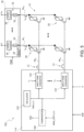
- FIG. 1 shows a circuit diagram of an in-memory computation device 10, hereinafter also referred to as IMC device 10, comprising a computation memory array (hereinafter indicated as memory array) 12, a line activation unit 14 and a reading unit 16.
- IMC device 10 comprising a computation memory array (hereinafter indicated as memory array) 12, a line activation unit 14 and a reading unit 16.
- the memory array 12 is of the non-volatile type and comprises a plurality of memory cells 20 organized in a matrix arrangement having M columns and N rows.
- a respective word line WL j and a respective bit line BL i are associated to each memory cell 20.
- the memory cells 20 are programmed to store each a respective computational weight g ij that may be used as a weight for performing an in-memory calculation.
- the line activation unit 14 provides a plurality of word line activation signals 21, one for each word line WL j , that are configured to each activate the memory cells 20 of a respective word line WL j .
- the line activation unit 14 receives an input vector X including a plurality of input values x 1 ,...,x N , one for each word line WL j .
- the word line activation signals 21 are pulses, in particular here rectangular pulses, each having a time width that is a function of the respective input value x j .
- the line activation unit 14 further receives an address signal ADR indicating which word lines WL j to activate for performing an in-memory calculation.
- the address signal ADR may be used to cause the activation, in use, only of some of the plurality of word lines WL 1 , ..., WL N , for example if the input vector X has a number of values smaller than the number N of rows of the memory array 12.
- the reading unit 16 comprises a plurality of digital detectors 22 and a biasing circuit 24.
- the biasing circuit 24 provides a bias voltage Vr to the bit lines BL 1 , ..., BL M .
- the biasing circuit 24 provides the same voltage Vr to all the bit lines BL 1 , ..., BL M .
- the biasing circuit 24 may provide bias voltages different with each other to the bit lines BL 1 ,...,BL M , depending on the specific application.
- the digital detectors 22 are each coupled to a respective bit line BL i and each provides an output signal y i indicative of a current I BL,i flowing through the respective bit line BL i , as discussed hereinafter in detail.
- the memory cells 20 each comprise a storing element 25 and a selection element 26.
- the storing element 25 of each memory cell 20 is a variable resistive element, in particular here based on a phase change material (PCM), such as a chalcogenide.
- PCM phase change material
- the computational weight g ij indicates the transconductance value of the storing element 25 of the respective memory cell 20, i.e. it is indicative of the programmed resistance of the storing element 25.
- a phase change material has at least two phase states, e.g. an amorphous phase and a crystalline phase, each having a respective resistivity.
- a phase change material may be transformed from one phase state to another by means of heat transfer, for example by using current pulses.
- each storing element 25 associated to the respective phase state is used to distinguish two or more logic states of the corresponding memory cell 20.
- the amorphous phase may have a higher resistance than the crystalline phase.
- a logic state '0', or reset state may be associated to the amorphous phase of the storing element 25.
- a logic state '1', or set state may be associated to the crystalline phase of the storing element 25.
- the selection element 26 is a switch, for example a BJT transistor, a diode or a MOS transistor, here an NMOS transistor, that is arranged in series with the respective storing element 25 and whose switching is controlled by the word line activation signal 21 of the respective word line WL j .
- the NMOS transistor forming the selection element 26 has a source coupled to, here directly connected to, the ground 29; a drain coupled to, here directly connected to, the second terminal of the storing element 25; and a gate coupled to, here directly connected to, the respective word line WL j .
- the storing element 25 and the selection element 26 form a current path of the respective memory cell 20; the selection element 26, in response to receiving the respective activation signal 21, closes the respective current path, thereby allowing the passage of a cell current i cell from the common node 28 to the ground 29.
- the IMC device 10 may further comprise interface circuits 30 coupled to the bit lines BL 1 , ..., BL M that may be used, for example, to programme the transconductance values g ij stored in the storing elements 25, in a per se known way.
- the digital detectors 22 each comprise an integration stage 33 and a counter stage 34 for each bit line BL i .
- the digital detectors 22 will be described hereinafter with respect to the digital detector 22 coupled to a generic bit line BL i of the plurality of bit lines BL 1 ,...,BL M .
- the integration stage 33 comprises a current mirror 35 that mirrors the bit line current I BL,i of the bit line BL i into an input node 36 of the respective integration stage 33.
- the current mirror 35 has a mirroring ratio 1:k, so that a mirrored bit line current k ⁇ I BL,i flows through the input node 36 of the integration stage 33.
- the current mirror 35 has a first branch, here formed by a respective PMOS transistor 37, coupled to the bit line BL i , and a second branch, here formed by a respective PMOS transistor 38, coupled to the respective integration stage 33.
- the sources of the PMOS transistors 37, 38 are coupled to a supply node 40, here at a voltage V DD , the gates of the PMOS transistors 37, 38 are mutually coupled together and to the drain of the PMOS transistor 37.
- the drain of the PMOS transistor 38 is coupled to, in particular here is directly connected to, the input node 36 of the integration stage 33.
- the integration stage 33 comprises a first integration circuit 41, a second integration circuit 42, and a switching circuit 43 coupled between the first and the second integration circuits 41, 42.
- the first and the second integration circuits 41, 42 are coupled to the input node 36 so as to receive the mirrored bit line current k ⁇ I BL,i .
- the first integration circuit 41 comprises a first inverter 45 having an output 46, a capacitor 47 of capacitance C A coupled at the output 46 of the first inverter 45, and a second inverter 48 whose input is coupled to the output 46 of the first inverter 45.
- the first inverter 45 has a supply node coupled to the input node 36 of the integration stage 33 ( figure 3 ) and receives at input a first control signal IN A .
- the first inverter 45 is biased by the mirrored bit line current k ⁇ I BL,i .
- the capacitor 47 has a first terminal coupled to the output node 46 of the first inverter 45 and a second terminal coupled to a reference potential node, here to ground.
- the output node 46 of the first inverter 45 is at a first integration voltage V A that drops across the capacitor 47.
- the second inverter 48 has a first sampling threshold, hereinafter referred to as first threshold V th1 , receives at input the first integration voltage V A and provides at output a first switch signal S1 as a function of the first threshold V th1 and the first integration voltage V A .
- the first switch signal S1 is a logic signal having a high logic value when the first integration voltage V A is smaller than the first threshold V th1 , and a low logic value when the first integration voltage V A is higher than the first threshold V th1 .
- the second integration circuit 42 comprises a first inverter 50 having an output 51, a capacitor 52 of capacitance C B coupled at the output 51 of the first inverter 50, and a second inverter 53 whose input is coupled to the output 51 of the first inverter 50.
- the first inverter 50 has a supply node coupled to the input node 36 of the integration stage 33 ( figure 3 ) and receives at input a second control signal IN B .
- the first inverter 50 is biased by the mirrored bit line current k ⁇ I BL,i .
- the capacitor 52 has a first terminal coupled to the output node 51 of the first inverter 50 and a second terminal coupled to a reference potential node, here to ground.
- the output node 51 of the first inverter 50 is at a second integration voltage V B dropping across the capacitor 51.
- the second inverter 53 has a second sampling threshold V th2 , hereinafter referred to as second threshold V th2 , receives at input the second integration voltage V B and provides at output a second switch signal S2 as a function of the second threshold V th2 and the second integration voltage V B .
- second threshold V th2 receives at input the second integration voltage V B and provides at output a second switch signal S2 as a function of the second threshold V th2 and the second integration voltage V B .
- the second switch signal S2 is a logic signal having a high logic value when the second integration voltage V B is smaller than the second threshold V th2 , and a low logic value when the second integration voltage V B is higher than the second threshold V th2 .
- the first threshold V th1 is equal to the second threshold V th2 ; however, the first threshold V th1 may be different to the second threshold V th2 , depending on the specific application.
- the switching circuit 43 is a latch formed by two inverters 55, 56 arranged in a ring configuration, a first switch 57 controlled by the first switch signal S1 and a second switch 58 controlled by the second switch signal S2.
- the switching circuit 43 has a first node 60 coupled to the input of the inverter 56 and the output of the inverter 55, and a second node 61 coupled to the output of the inverter 56 and the input of the inverter 55.
- the first node 60 provides the first control signal IN A .
- the second node 61 provides the second control signal IN B .
- the first switch 57 is coupled between the first node 60 and a node at a voltage V' DD
- the second switch 58 is coupled between the second node 61 and the node at the voltage V' DD .
- the voltage V' DD may be equal or different to the voltage V DD of the supply node 40.
- the digital detector 22 may comprise a voltage scaling circuit, for example a transistor, here not shown, whose source and drain terminals are coupled between the supply node 40 and the input node 36 of the integration stage 33.
- the switching circuit 43 also receives an enable signal EN, which controls the activation of the switching circuit 43.
- the enable signal EN may be used to keep the switching circuit 43 off when not in use, thereby allowing to optimize power consumption.
- the enable signal EN may be used to set the switching circuit 43 in a defined state, for example upon turning on of the IMC device 10.
- the charge counter stage 34 is coupled to the first and the second nodes 60, 61 of the switching circuit 43.
- the charge counter stage 34 comprises an inverter 63, whose input is coupled to the second node 61, and a counter comprising an inverter 65 whose input is coupled to the first node 60 and a plurality of D flip-flops 67 including a first flip-flop 67.2, a second flip-flop 67.3 and a last flip-flop 67.F, wherein F is the number of bits of the output signal y i .
- the counter of the charge counter stage 34 has F-1 flip-flops 67.
- the output of the inverter 63 provides the first bit yi(1), i.e. the least significant bit, of the output signal y i .
- the output of the inverter 63 may be used, at the end of a calculation performed by the IMC device 10, as the least significant bit y i (1) of the output signal y i .
- the flip-flops 67 are cascaded one with the other, in sequence from the first flip-flop 67.2 to the last flip-flop 67.F.
- the flip-flops 67 each have a clock input (CK-input), a data input (D-input), a Q-output, and a Q -output.
- the CK-input of the first flip-flop 67.2 is coupled to the output of the inverter 65.
- the Q -output of the first flip-flop 67.2 is fed back to the D-input of the first flip-flop 67.2.
- the Q-output of the first flip-flop 67.2 forms the second bit y i (2) of the output signal y i .
- the CK-input of the second flip-flop 67.3 is coupled to the Q -output of the first flip-flop 67.2.
- the Q -output of the second flip-flop 67.3 is fed back to the D-input of the second flip-flop 67.3.
- the Q-output of the second flip-flop 67.3 forms the third bit y i (2) of the output signal y i .
- the CK-input of the last flip-flop 67.F is coupled to the Q -output of the F-1-th flip-flop.
- the Q- output of the last flip-flop 67.F is fed back to the D-input of the last flip-flop 67.F.
- the Q-output of the last flip-flop 67.F forms the most significant bit yi(F) of the output signal yi.
- the first inverter 45 of the first integration circuit 41 is a CMOS inverter formed by the series circuit of a PMOS transistor 70 and an NMOS transistor 71, mutually coupled at the output node 46.
- the PMOS and NMOS transistors 70, 71 receive the first control signal IN A at the respective gate terminals.
- the source of the PMOS transistor 70 is coupled to the input node 36 of the integration stage 33.
- the second inverter 48 of the first integration circuit 41 is a CMOS inverter formed by the series circuit of a PMOS transistor 72 and an NMOS transistor 73, mutually coupled at a node 74 providing the first switch signal S1.
- the first threshold V th1 of the second inverter 48 is the switching threshold of the second inverter 48, and therefore depends on the properties, for example the threshold or the on-resistance, of the PMOS and NMOS transistors 72, 73.
- the switching threshold may be the input voltage for which the output of the inverter has the high logic value or the input voltage for which the output of the inverter has the low logic value.
- the switching threshold of the second inverter 48 may be defined as the operating point at which the respective input voltage, i.e. the first integration voltage V A , is equal to the respective output voltage, i.e. the first switch signal S1.
- the first inverter 50 of the second integration circuit 42 is a CMOS inverter formed by the series circuit of a PMOS transistor 75 and an NMOS transistor 76, mutually coupled at the output node 51.
- the PMOS and NMOS transistors 75, 76 receive the second control signal IN B at the respective gate terminals.
- the source of the PMOS transistor 75 is coupled to the input node 36 of the integration stage 33.
- the second inverter 53 of the second integration circuit 42 is a CMOS inverter formed by the series circuit of a PMOS transistor 77 and an NMOS transistor 78, mutually coupled at a node 79 providing the second switch signal S2.
- the second threshold V th2 of the second inverter 53 is the switching threshold of the second inverter 53, i.e. depends on the properties of the PMOS and NMOS transistors 77, 78.
- the switching threshold depends on the gate-source voltage that allows a current to flow through the source-drain path of the PMOS and NMOS transistors 77, 78.
- the first and the second inverters 55, 56 of the switching circuit 43 are cross-coupled CMOS inverters each comprising a respective PMOS transistor 80 and a respective NMOS transistor 81 mutually coupled in series between a supply node, here at the voltage V' DD , and ground.
- first and the second inverters 55, 56 of the switching circuit 43 also comprise each a respective enabling switch, here a PMOS transistor 82, that is coupled between the supply node at the voltage V' DD and the PMOS transistor 80 of the respective inverter.
- the PMOS transistors 82 are controlled by the enabling signal EN.
- bit line current I BL,i of the bit line BL i is mirrored into the integration stage 33 of the respective digital detector 22.
- Figure 4 shows an example of the time behaviour of the first control signal IN A , the first integration voltage V A and the second integration voltage V B of the digital detector 22 of figure 2 .
- the first integration voltage V A is below the first threshold V th,1 . Accordingly, the PMOS transistor 72 of the second inverter 48 is on and the NMOS transistor 73 of the second inverter 48 is off. Therefore, the first switch signal S1 (here not shown) has the high value and the first switch 57 is open.
- the first control signal IN A has the low value.
- the second control signal IN B has the high value. Therefore, with respect to the first inverter 50 of the second integration circuit 42, for t 0 ⁇ t ⁇ t 1 , the PMOS transistor 75 is off and the NMOS transistor 76 is on.
- the mirrored bit line current k ⁇ I BL,i flows, from the input node 36, only through the first inverter 45 of the first integration circuit 41 and not through the first inverter 50 of the second integration circuit 42.
- the mirrored bit line current k ⁇ I BL,i flows through the PMOS transistor 70 and charges the capacitor 47.
- the first integration voltage V A thus increases in time for t 0 ⁇ t ⁇ t 1 .
- the first integration voltage V A increases linearly in time for t 0 ⁇ t ⁇ t 1 ; however, the behaviour of the first integration voltage V A depends on the specific behaviour of the bit line current I BL,i in the time interval t 0 ⁇ t ⁇ t 1 .
- the first control signal IN A assumes the high value at a time instant t 2 .
- the time delay between instants t 1 and t 2 may correspond, for example, to the propagation delay of the second inverter 48 of the first integration circuit 41 and/or the switching time of the first switch 57.
- the mirrored bit line current I BL,i keeps charging the capacitor 47; accordingly, the first integration voltage V A increases up to a maximum value (instant t 2 ).
- the second control signal IN B (here not shown) assumes the low value (the inverter 56 of the switching circuit 43 receives the first control signal IN A at input).
- the PMOS transistor 70 and the NMOS transistor 71 of the first inverter 45 of the first integration circuit 41 are off and, respectively, on.
- the second control signal IN B has the low value
- the PMOS transistor 75 and the NMOS transistor 76 of the first inverter 50 of the second integration circuit 42 are on and, respectively, off.
- the mirrored bit line current k ⁇ I BL,i flows, from the input node 36, only through the first inverter 50 of the second integration circuit 42 and not through the first inverter 45 of the first integration circuit 41.
- the mirrored bit line current k ⁇ I BL,i flows through the PMOS transistor 75 and charges the capacitor 52 of the second integration circuit 42.
- the second integration voltage V B thus increases in time from the time instant t 2 .
- the second integration voltage V B increases linearly in time for t>t 2 ; however, the behaviour of the second integration voltage V B depends on the specific behaviour of the bit line current I BL,i .
- the capacitor 47 of the first integration circuit 41 discharges through the NMOS transistor 71 of the first inverter 45.
- the first integration voltage V A thus decreases to zero.
- the second control signal IN B assumes the high value, similarly to what has been discussed above for the first control signal IN A in correspondence of time instant t 2 .
- the second switch signal S2 switches to the low value and the second switch 58 closes, so that the second node 61 is at the voltage V' DD and, accordingly, the second control signal IN B assumes the high value.
- the time delay between instants t 3 and t 4 may correspond, for example, to the propagation delay of the second inverter 53 of the second integration circuit 42 and/or the switching time of the second switch 58.
- the mirrored bit line current k ⁇ I BL,i keeps charging the capacitor 52 of the second integration circuit 42; accordingly, the second integration voltage V B increases up to a maximum value (instant t 4 ).
- the switching circuit 43 keeps the first control signal IN A at the high value and the second control signal IN B at the low value.
- the first control signal IN A assumes the low value again, in response to the second control signal IN B assuming the high value.
- the mirrored bit line current k ⁇ I BL,i returns to charging the capacitor 47 of the first integration circuit 41 up to a time instant t 6 , similarly to what has been discussed for t 1 ⁇ t ⁇ t 2 .
- the mirrored bit line current k ⁇ I BL,i charges the capacitor 52 of the second integration circuit 42 up to a time instant t 7 , similarly to what has been discussed for t 2 ⁇ t ⁇ t 4 .
- the counter stage 34 in particular the flip-flops 67, counts the number of switching events of the first control signal IN A , in particular in this embodiment counts the number of rising edges of the first control signal IN A .
- the digital detectors 22 each measure the bit line current I BL,i of the respective bit line BL i by performing a number of successive sampling iterations.
- the integration stage 33 In each sampling iteration, for example with respect to a sampling iteration wherein the mirrored bit line current k ⁇ I BL,i flows through the first integration circuit 41, the integration stage 33 generates the first integration voltage V A as the time integral of the mirrored bit line current k ⁇ I BL,i , compares the first integration voltage V A with the first threshold V th,1 and, in response to the first integration voltage V A reaching the first threshold V th,1 , resets the first integration voltage V A , in particular here by switching the first control signal IN A .
- the counter stage 34 updates the respective output signal y i in response to the first integration voltage V A reaching the first threshold V th,1 .
- the least significant bit of the output signal yi is the value of the second control signal IN B at the end of the computation performed by the IMC device 10.
- the digital detectors 22 sample each the respective bit line current I BL,i by converting the bit line current I BL,i into a number of charge packets and counting said charge packets, wherein each charge packet corresponds to the charge accumulated on the capacitors 47, 52 that causes a switch of the second inverters 48, 53.
- the capacitors 47, 52 may have a small capacitance if compared to a case wherein the bit line current is integrated all at once onto a single capacitor of capacitance C tot .
- the capacitance of the capacitors 47, 52 may be smaller than the capacitance C tot by a factor 2 F , wherein F is the number of bits of the output signal yi.
- the digital detectors 22 may have a low die area occupancy and, accordingly, the IMC device 10 may have low manufacturing costs.
- the digital detectors 22 each start discretizing the respective bit line current I BL,i while the bit line current I BL,i flows through the respective bit line BL i . Therefore, the output signal yi may be ready soon after an end of a computation performed by the IMC device 10 or soon after the respective bit line current I BL,i stops.
- the digital detectors 22 may sample each the respective bit line current I BL,i until the digital detectors 22 receive a stop signal, for example from a user of the IMC device 10 or from the word line activation unit 14, indicating the end of the computation performed by the IMC device 10.
- the digital detectors 22 may have a fast measurement time, thereby allowing the IMC device 10 to have a low computation time.
- the switching circuit 43 disables the first integration circuit 41 and enables the second integration circuit 42, in response to the first integration signal V A reaching the first threshold V th,1 , and enables the first integration circuit 41 and disables the second integration circuit 42, in response to the second integration signal V B reaching the second threshold V th,2 .
- bit line current I BL,i This allows the bit line current I BL,i to be sampled alternatively by the first integration circuit 41 and the second integration circuit 42, thereby allowing the bit line current I BL,i to charge the capacitor 47 while the capacitor 52 is discharging, and to charge the capacitor 52 while the capacitor 47 is discharging. By doing so, no charge may be lost during the sampling and the digital detector 22 may achieve a high measurement accuracy of the bit line current I BL,i .
- MAC multiply and accumulate
- the cell current i cell that each memory cell 20 sinks depends on the transconductance g ij of the respective storing element 25 and the activation time of the respective selection element 26, i.e. on the pulse length of the respective word line activation signal 21.
- each cell current i cell depends on the respective transconductance value g ij .
- the time duration of each cell current i cell depends on the respective activation time.
- an electric charge may be associated to each cell current i cell ; said electric charge is a function of the respective transconductance value g ij and the respective activation time.
- the electric charge associated to each cell current i cell is a function of the product g ij ⁇ x j .
- each bit line BL i the respective bit line current I BL,i is a summation of the cell currents i cell . Therefore, the total electric charge associated to each bit line current I BL,i is a function of the multiply and accumulate operation g i1 ⁇ x 1 + g i2 ⁇ x 2 + ... + g iN ⁇ x N .
- each output signal yi which is obtained by measuring the respective bit line current I BL,i , in particular by integrating the respective bit line current I BL,i , is indicative of the MAC operation g i1 ⁇ x 1 + g i2 ⁇ x 2 + ... + g iN ⁇ x N .
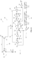
- FIG. 5 shows a different embodiment of the present IMC device, here indicated by 100.
- the IMC device 100 has a general structure similar to IMC device of figure 1 ; therefore, elements in common are indicated by the same reference numbers and are not further described in detail.
- the IMC device 100 comprises the memory array 12, here shown only in part, a line activation unit 114 and the reading unit 16.
- the reading unit 16 comprises also here the biasing circuit 24 and the digital detectors 22.
- the word line activation unit 114 receives the input signal X including the plurality of input values x 1 ,...,x N , and provides the plurality of word line activation signals 21 each as a function of a respective input value x j .
- the line activation circuit 114 comprises an oscillator 120 providing a timer signal TM ⁇ L:1> having L bits, and a plurality of comparators 122, one for each word line WL 1 ,...,WL N .
- the plurality of comparators 122 receive each the timer signal TM ⁇ L:1> and a respective input value x j and, in response, provide a respective word line activation signal 21.
- the oscillator 120 shown in detail in figures 6 and 7 , comprises a current generation portion 125 generating an oscillator current, here a mirrored current p ⁇ I OSC , and a counting portion 126 that generates the timer signal TM ⁇ L:1> from the oscillator current.
- the current generation portion 125 comprises a current source 127 generating a supply current I OSC and a current mirror 128 that mirrors the supply current I OSC into an input node 129 of the counting portion 126.
- the supply current I OSC may be for example equal to a maximum current that may flow through a bit line BL i , i.e. the current that flows in the bit line BL i when all the memory cells 20 associated to the bit line BL i are activated.
- the supply current I OSC may have a different value, depending on the specific application.
- the current mirror 128 has a mirroring ratio 1:p, so that the mirrored current that flows through the input node 129 of the counting portion 126 is p ⁇ I OSC .
- the current mirror 128 has a first branch, here formed by a respective PMOS transistor 130, coupled to the current source 127, and a second branch, here formed by a respective PMOS transistor 131, coupled to the counting portion 126.
- the sources of the PMOS transistors 130, 131 are coupled to a supply node 132, here at the voltage V DD , the gates of the PMOS transistors 130, 131 are mutually coupled together and to the drain of the PMOS transistor 130.
- the drain of the PMOS transistor 131 is coupled to, in particular here is directly connected to, the input node 129 of the counting portion 126.
- the counting portion 126 of the oscillator 120 comprises an integration stage 133, formed here by a first integration circuit 134, a second integration circuit 135 and a switching circuit 136 coupled between the first and the second integration circuits 134, 135, and a counter stage 137 which is coupled to the integration stage 133 and provides the timer signal TM ⁇ L:1>.
- the first and the second integration circuits 134, 135 are coupled to the input node 129 so as to receive the mirrored current p ⁇ I OSC .
- the first integration circuit 134 comprises a first inverter 140 having an output 141, a capacitor 142 of capacitance C' A coupled at the output 141 of the first inverter 140, and a second inverter 143 whose input is coupled to the output 141 of the first inverter 140.
- the first inverter 140 has a supply node coupled to the input node 129 of the counting portion 126 ( figure 7 ) and receives at input a first oscillator control signal OS A .
- the first inverter 140 is biased by the mirrored current p ⁇ I OSC .
- the capacitor 142 has a first terminal coupled to the output node 141 of the first inverter 140 and a second terminal coupled to a reference potential node, here to ground.
- the output node 141 of the first inverter 140 is at a first oscillator integration voltage V' A that drops across the capacitor 142.
- the second inverter 143 has a first oscillator threshold V' th1 , hereinafter simply referred to as first threshold V' th,1 , receives at input the first oscillator integration voltage V' A and provides at output a first oscillator switch signal S'1 as a function of the first threshold V' th1 and the first oscillator integration voltage V' A .
- first threshold V' th,1 receives at input the first oscillator integration voltage V' A and provides at output a first oscillator switch signal S'1 as a function of the first threshold V' th1 and the first oscillator integration voltage V' A .
- the first oscillator switch signal S'1 when the first oscillator integration voltage V' A is smaller than the first threshold V' th1 , the first oscillator switch signal S'1 has a high logic value. When the first oscillator integration voltage V' A is higher than the first threshold V' th1 , the first oscillator switch signal S'1 has a low logic value.
- the second integration circuit 135 comprises a first inverter 146 having an output 147, a capacitor 148 of capacitance C' B coupled at the output 147 of the first inverter 146, and a second inverter 149 whose input is coupled to the output 147 of the first inverter 146.
- the first inverter 146 has a supply node coupled to the input node 129 of the counting portion 126 ( figure 7 ) and receives at input a second oscillator control signal OS B .
- the first inverter 146 is biased by the mirrored current p ⁇ I OSC .
- the capacitor 148 has a first terminal coupled to the output node 147 of the first inverter 146 and a second terminal coupled to a reference potential node, here to ground.
- the output node 147 of the first inverter 146 is at a second oscillator integration voltage V' B dropping across the capacitor 148.
- the second oscillator switch signal S'2 when the second oscillator integration voltage V B is smaller than the second threshold V' th2 , the second oscillator switch signal S'2 has a high logic value. When the second oscillator integration voltage V' B is higher than the second threshold V' th2 , the second oscillator switch signal S'2 has a low logic value.
- the switching circuit 136 is a latch formed by two inverters 150, 151 arranged in a ring configuration, a first switch 153 controlled by the first oscillator switch signal S'1 and a second switch 154 controlled by the second oscillator switch signal S'2.
- the switching circuit 136 has a first node 156 coupled to the input of the inverter 151 and the output of the inverter 150, and a second node 157 coupled to the output of the inverter 151 and the input of the inverter 150.
- the first node 156 provides the first oscillator control signal OS A .
- the second node 157 provides the second oscillator control signal OS B .
- the first switch 153 is coupled between the first node 156 and a node at the voltage V' DD
- the second switch 154 is coupled between the second node 157 and the node at the voltage V' DD .
- the voltage V' DD of the counting portion 126 of the oscillator 120 may be equal to the voltage V' DD of the integration stage 33 of the digital detector 22 ( figure 2 ).
- the switching circuit 136 also receives an oscillator enable signal EN', which controls the activation of the switching circuit 136.
- the oscillator enable signal EN' may be used to keep the switching circuit 136 off when not in use, thereby allowing to optimize power consumption.
- the enable signal EN' may be used to set the switching circuit 136 in a defined state, for example upon turning on of the IMC device 10.
- the counter stage 137 is coupled to the first and the second nodes 156, 157 of the switching circuit 136.
- the output of the inverter 159 provides the first bit TM(1), i.e. the least significant bit, of the timer signal TM.
- the flip-flops 161 are cascaded one with the other, in sequence from the first flip 161.2 to the last flip-flop 161.L.
- the flip-flops 161 each have a clock input (CK-input), a data input (D-input), a Q-output, and a Q -output.
- the CK-input of the first flip-flop 161.2 is coupled to the output of the inverter 160.
- the Q -output of the first flip-flop 161.2 is fed back to the D-input of the first flip-flop 161.2.
- the Q-output of the first flip-flop 161.2 forms the second bit TM(2) of the timer signal TM ⁇ L:1>.
- the CK-input of the second flip-flop 161.3 is coupled to the Q -output of the first flip-flop 161.2.
- the Q -output of the second flip-flop 161.3 is fed back to the D-input of the second flip-flop 161.3.
- the Q-output of the second flip-flop 161.3 forms the third bit TM(3) of the timer signal TM ⁇ L:1>.
- the CK-input of the last flip-flop 161.L is coupled to the Q -output of the L-1-th flip-flop.
- the Q- output of the last flip-flop 161.L is fed back to the D-input of the last flip-flop 161.L.
- the Q-output of the last flip-flop 161.L forms the most significant bit TM(L) of the timer signal TM ⁇ L:1>.
- the source of the PMOS transistor 165 is coupled to the input node 129 of the integration stage 133 of the oscillator 120.
- the first threshold V' th1 of the second inverter 143 is the switching threshold of the second inverter 143, and therefore depends on the properties, for example the threshold or the on-resistance, of the PMOS and NMOS transistors 168, 169.
- the switching threshold may be the input voltage for which the output of the inverter has the high logic value or the input voltage for which the output of the inverter has the low logic value.
- the switching threshold of the second inverter 143 may be defined as the operating point at which the respective input voltage, i.e. the first oscillator integration voltage V' A , is equal to the respective output voltage, i.e. the first oscillator switch signal S'1.
- the first inverter 146 of the second integration circuit 135 is a CMOS inverter formed by the series circuit of a PMOS transistor 171 and an NMOS transistor 172, mutually coupled at the output node 173.
- the PMOS and NMOS transistors 172, 173 receive the second oscillator control signal OS B at the respective gate terminals.
- the source of the PMOS transistor 171 is coupled to the input node 129 of the counting portion 126 of the oscillator 120.
- the second threshold V' th2 of the second inverter 149 is the switching threshold of the second inverter 149, and therefore depends on the properties, for example the threshold or the on-resistance, of the PMOS and NMOS transistors 175, 176.
- the switching threshold may be the input voltage for which the output of the inverter has the high logic value or the input voltage for which the output of the inverter has the low logic value.
- the switching threshold of the second inverter 149 may be defined as the operating point at which the respective input voltage, i.e. the second oscillator integration voltage V' B , is equal to the respective output voltage, i.e. the second oscillator switch signal S'2.
- the first and the second inverters 150, 151 of the switching circuit 136 are cross-coupled CMOS inverters each comprising a respective PMOS transistor 180 and a respective NMOS transistor 181 mutually coupled in series between a supply node, here at the voltage V' DD , and ground.
- first and the second inverters 150, 151 of the switching circuit 136 also comprise each a respective enabling switch, here a PMOS transistor 182, that is coupled between the supply node at the voltage V' DD and the PMOS transistor 180 of the respective inverter.
- the PMOS transistors 182 are controlled by the oscillator enabling signal EN'.
- the oscillator 120 in particular the respective integration stage 133, has a circuit diagram that is equal to the circuit diagram of any one of the digital detectors 22 of figures 2 and 3 , in particular of the respective integration stage 33.
- the oscillator 120 generates the timer signal TM ⁇ L:1> from the oscillator current I OSC in the same way as any one of the digital detectors 22 generates the output signal y i from the respective bit line current I BL,i .
- the oscillator 120 generates the timer signal TM ⁇ L:1> by performing a number of successive timing iterations.
- the integration stage 133 In each timing iteration, for example with respect to a timing iteration wherein the mirrored oscillator current p ⁇ I OSC flows through the first integration circuit 134, the integration stage 133 generates the first integration oscillation voltage V' A as the time integral of the mirrored oscillator current p ⁇ I OSC , compares the first oscillator integration voltage V' A with the first threshold V' th,1 and, in response to the first oscillator integration voltage V' A reaching the first threshold V' th,1 , resets the first oscillator integration voltage V' A , in particular here by switching the first oscillator control signal OS A .
- the counter stage 137 updates the timer signal TM ⁇ L:1> in response to the first oscillator integration voltage V' A reaching the first threshold V' th,1 .
- the least significant bit of the timer signal TM is the value of the second oscillator control signal OS B .
- the oscillator 120 samples the oscillator current I OSC by converting the oscillator current I OSC into a number of charge packets and counting said charge packets, wherein each charge packet corresponds to the charge accumulated on the capacitors 142, 148 that causes a switch of the second inverters 143, 149.
- the timer signal TM ⁇ L:1> is updated at a frequency f u given by the switching events of the first oscillator control signal OS A (similarly to what discussed for the first control signal IN A with reference to figure 4 ).
- the update frequency f u thus depends on the value of the oscillator current I OSC , the mirror factor p of the current mirror 128, the capacitances C' A , C' B , and the first and second thresholds V' th,1 , V' th,2 of the second inverters 143, 149.
- Figure 8 shows in detail an embodiment of the input-time converter 122 of a word line WL j of the plurality of word lines WL 1 ,...,WL M comprising a comparator 190 receiving the timer signal TM ⁇ L:1> and the respective input value x j and providing, in response, a match signal MTC; and a pulse generation circuit, here formed by a NAND logic gate 191 and an inverter 192, providing the respective word line activation signal 21.
- the input value x j and the timer signal TM ⁇ L:1> are digital signals.
- the comparator 190 for example a bit checking circuit based on a XOR logic gate, compares the input value x j and the timer signal TM ⁇ L:1> and asserts the match signal MTC to the high logic value when the timer signal TM ⁇ L:1> becomes equal to the input value x j .
- the NAND logic gate 191 receives the match signal MTC and an address enable signal ADR_EN indicating if the word line WL j has to be activated during the performance of an in-memory calculation.
- the address enable signal ADR_EN may have a high logic value if the word line WL j has to be activated during the in-memory calculation.
- the inverter 192 is coupled at input to the output of the NAND logic gate 191 and provides at output the word line activation signal 21.
- the inverter 192 operates as a driver circuit for the respective word line WL j .
- the input-time converter 122 keeps the respective word line activation signal 21 to the high logic value (i.e. thereby here activating the selection elements 26 of the memory cells 20 coupled to the word line WL j ) as long as the timer signal TM ⁇ L:1> is different from the input value x j .
- the word line activation signals 21 each have a respective activation length T j that is proportional to the update frequency f u of the timer signal TM ⁇ L:1> and the respective input value x j .
- Figure 9 shows, by way of example, the word line activation signals 21 of the first word line WL 1 and the last word line WL N .
- the timer signal TM ⁇ L:1> of the oscillator 120 is reset to a start value, for example to zero, and the input-time converters 122 switch each the respective word line activation signal 21 to the high value.
- the input value x 1 associated to the first word line WL 1 is smaller than the input value x N associated to the last word line WL N ; therefore, the input-time converter 122 associated to the first word line WL 1 keeps the respective word line activation signal 21 to the high value for a time shorter with respect to the input-time converter 122 associated to the last word line WL N .
- the fact that the oscillator 120 generates the timer signal TM ⁇ L:1> from the oscillator current I OSC in the same way as the digital detectors 22 each generate the respective output signal yi from the respective bit line current I BL,i , in particular the fact that the respective integration circuits 33, 133 have the same circuit diagram, allows to obtain a strong correlation between the timer signal TM ⁇ L:1> and the output signals y 1 ,...,y M .
- the oscillator 120 may comprise a computation-end comparator 193, as indicated by a dashed line in figure 5 .
- the computation-end comparator 193 receives the timer signal TM ⁇ L:1> and a max count signal MAX_COUNT ⁇ L:1> and provides, in response, an end-count signal END.
- the max count signal MAX_COUNT ⁇ L:1> may be received from a user of the IMC device 10 and indicates the maximum duration of a calculation performed by the IMC device 10.
- the max count signal MAX_COUNT ⁇ L:1> may indicate a maximum duration equal to or higher than the time that any of the output signals yi would take to reach the maximum value, e.g. all F bits equal to 1, when all the cells 20 associated to the bit line BL i are activated.
- the max count signal MAX_COUNT ⁇ L:1> may indicate a smaller maximum duration, for example if it is desired to obtain a shorter computation time by the IMC device 10.
- the oscillator 120 may comprise, with reference to figure 7 , a first and a second stop switches, here a first and a second NMOS transistors 194, 195, that are configured to stop the oscillator 120 from updating the timer signal TM.
- the first and the second NMOS transistors 194, 195 have a drain terminal coupled to the output nodes 141, 173 of the first and, respectively, the second integration circuits 134, 135; and a source terminal coupled to a reference, here ground.
- the first and the second NMOS transistors 194, 195 receive, at the respective gate terminals, the end-count signal END.
- the end-computation comparator 195 switches the end signal END to the high logic value, thereby turning on the first and the second NMOS transistors 194, 195 and short-circuiting the output nodes 141, 173 of the first and the second integration circuits 134, 135 to ground.
- the oscillator 120 stops updating the timer signal TM.
- Figure 10 shows a different embodiment of the integration stage of any of the digital detectors 22 of the reading unit 16, here indicated as integration stage 220.
- the integration stage 220 differs from the integration stage 33 shown in figure 3 in that it comprises a first and a second stop switches, here a first and a second NMOS transistors 196, 197, that are configured to stop the digital detectors 22 from measuring the respective bit line current I BL,i .
- the first and the second NMOS transistors 196, 197 have a drain terminal coupled to the output nodes 46, 51 of the first and, respectively, the second integration circuits 41, 42; and a source terminal coupled to a reference, here ground.
- the first and the second NMOS transistors 196, 197 receive, at the respective gate terminals, the end-count signal END.
- the end-computation comparator 193 switches the end signal END to the high logic value, thereby turning on the first and the second NMOS transistors 196, 197 and short-circuiting the output nodes 46, 51 of the first and the second integration circuits 41, 42 to ground.
- the first and the second integration circuits 41, 42 stop integrating the bit line current BL i .
- the end-count signal END may be used to determine the end of the MAC calculation by the IMC device 100.
- FIG 11 shows a further embodiment of the present IMC device, here indicated by 200.
- the IMC device 200 has a general structure similar to the IMC device 100 of figure 5 ; therefore, elements in common are indicated by the same reference numbers and not further described.
- the IMC device 200 comprises the memory array 12, the reading unit 16 and the word line activation unit 114.
- the reading unit 16 comprises the plurality of digital detectors 22, one for each bit line BL i .
- the word line activation unit 114 comprises the oscillator 120 and the input-time converters 122 providing the word line activation signals 21.
- the IMC device 200 further comprises a reference memory array 205 comprising one or more reference cells, here a plurality of reference cells 206, of the non-volatile type.
- the reference memory array 205 may be a portion of the memory array 12 or may be a separate memory array.
- the reference cells 206 have the same circuit configuration as the memory cells 20 of the memory array 12.
- the reference cells 206 comprise each a storing element 210 and a selection element 211, in particular equal to the storing element 25 and, respectively, the selection element 26 of the memory cells 20.
- the storing element 210 is based on the same technology that is used to obtain the storing element 25.
- the storing element 25 is based on a PCM material
- the storing element 210 is also based on a PCM material, in particular the same PCM material.
- the reference cells 206 are programmed to store respective reference transconductance values, which may be equal or different to one another, depending on the specific application.
- the number of reference cells 206 and the respective reference transconductance values may be chosen, at the design stage, so that the reference memory array 205 is a statistically significant sample of the memory array 12.
- the reference memory array 205 has an overall reference transconductance value g ref that statistically represents an overall transconductance of the memory array 12.
- the overall transconductance of the memory array 12 may be equal to the transconductance that the memory array 12 would have if all the reference cells 20 are activated at the same time.
- the number of reference cells 206 may be higher than one hundred.
- the reference cells 206 may be programmed so that the overall transconductance g ref of the reference memory array 205 is equal to a mean value of the overall transconductance of the memory array 12.
- the mean value may represent the average transconductance value that the memory array 12 has in use, for example as determined during a calibration or initialization step of the IMC device 10.
- the storing elements 210 have a first terminal that is coupled to a common node 213 and a second terminal coupled to a reference potential node, here to ground 29, through the selection element 211.
- the reference cells 206 all share a same reference bit line BL ref .
- the selection elements 211 are each formed by a respective switch, here an NMOS transistor, that is arranged in series with the respective storing element 210.
- the selection elements 211 of all the reference cells 206 are controlled by a same reference activation signal REF, which for example may be generated by the word line activation unit 114 or by other components of the IMC device 200, here not shown.
- REF reference activation signal
- the selection elements 211 may be controlled each by a respective reference activation signal, different one from the other, depending on the number of reference cells 206 that is intended to activate.
- the reference activation signal REF may keep all the reference memory cells 206 activated for the whole duration of a computation performed by the IMC device 10.
- the reference memory array 205 forms the current source 127.
- the common node 213 of the reference memory array 205 is coupled to the first branch of the current mirror 128, in particular to the drain of the PMOS transistor 130.
- the reference memory array 205 is biased by a fixed voltage, here the voltage V DD of the supply node 132, but the oscillator current I OSC depends on the transconductance values of the reference cells 206.
- the IMC device 200 may be subject to a temperature variation that may affect the transconductance values g ij of the memory cells 20. Moreover, the transconductance values g ij of the memory cells 20 may be subject to drifts; for example, in case the memory cells 20 are PCM memory cells, the storing elements 25 may be subject to aging phenomena such as amorphization.
- Such deviations of the transconductance values g ij from the programmed values may change the bit line current I BL,i , thereby causing errors in the output signal yi.
- a change in the reference transconductance value g ref would cause a change in the oscillator current I OSC and, therefore, a change in the update frequency f u of the timer signal TM ⁇ L:1> that compensate the change in the transconductance values g ij of the memory cells 20.
- the memory cells 20 undergo a drift that causes an increase in the respective transconductance values g ij , the corresponding bit line current I BL,i would also increase.
- the reference transconductance value g ref would increase, thereby causing an increase in the oscillator current I OSC .
- the higher transconductance values g ij are compensated by inducing a reduced activation time of the word line WL j , so that the bit line current I BL,i is, as a first approximation, not affected by the drift in the transconductance values g ij .
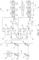
- FIG. 12 shows a different embodiment of the present IMC device, here indicated by 300.
- the IMC device 300 has a general structure similar to the IMC devices 10, 100, 200; therefore, elements in common are indicated by the same reference numbers and are not further described.
- Figure 12 shows only the elements that are useful for understanding the present embodiment, whereas elements and components that may be present in the final IMC device 300 and are not relevant for understanding the present embodiment are not shown.
- the IMC device 300 comprises the memory array 12 and a reading unit 316 having a plurality of digital detectors 322, one for each bit line BL 1 , ..., BL M .
- the digital detectors 322 will be described hereinafter with respect to the digital detector 322 of the bit line BL M , which is shown in detail in figure 12 .
- the digital detector 322 comprises an integration stage 330 and a counter stage 331.
- the integration stage 330 comprises a first integration circuit 334, a second integration circuit 335, and a switching circuit 336 coupled between the first and the second integration circuits 334, 335.
- the switching circuit 336 comprises a first switch 337 and a second switch 338 that couple the bit line BL M to the first integration circuit 334 and, respectively, to the second integration circuit 335.
- the first and the second switches 337, 338 are controlled by a selection signal SEL so that if the first switch 337 is open then the second switch 338 is closed and if the first switch 337 is closed then the second switch 338 is open.
- the switching circuit 336 further comprises an inverter 339 that receives the selection signal SEL and is coupled at output to the first switch 337.
- the switching circuit 336 allows the bit line current I BL,M to flow either through the first integration circuit 334 or through the second integration circuit 335.
- the first integration circuit 334 comprises a first operational amplifier 341, a feedback circuit 342, and a second operational amplifier 343.
- the first operational amplifier 341 has an inverting input coupled to the first switch 337 of the switching circuit 336, receives a read voltage Vr at a non-inverting input, and has an output 344 providing a voltage V q1 .
- the feedback circuit 342 is coupled between the inverting input and the output 344 of the first operational amplifier 341 and is formed by a parallel circuit comprising a feedback capacitor 345 and a switch 346.
- the second operational amplifier 343 has the non-inverting input coupled to the output 344 of the first operational amplifier 341, receives the first sampling threshold voltage V th,1 at the inverting input, and has an output 347 providing a first output voltage V out1 .
- the commutation of the switch 346 is controlled by the first output voltage V out,1 .
- the second integration circuit 335 comprises a first operational amplifier 350, a feedback circuit 351, and a second operational amplifier 352.
- the first operational amplifier 350 has an inverting input coupled to the second switch 338 of the switching circuit 336, receives the read voltage Vr at a non-inverting input, and has an output 353 providing a voltage V q2 .
- the feedback circuit 351 is coupled between the inverting input and the output 353 of the first operational amplifier 350 and is formed by a parallel circuit comprising a feedback capacitor 355 and a switch 356.
- the second operational amplifier 352 has the non-inverting input coupled to the output 353 of the first operational amplifier 350, receives the second sampling threshold voltage V th,2 at the inverting input, and has an output 357 providing a second output voltage V out,2 .
- the commutation of the switch 356 is controlled by the second output voltage V out,2 .
- the first and the second threshold voltages V th,1 , V th,2 are here equal; however, the first and the second threshold voltages V th,1 , V th,2 may be different one from the other.
- the charge counter stage 331 comprises a first counting circuit, here formed by a plurality of flip-flops 360, coupled to the first integration circuit 334, and providing a first intermediate output signal y' M ; and a second counting circuit, here formed by a plurality of flip-flops 361, coupled to the second integration circuit 335, and providing a second intermediate output signal y" M .
- the flip-flops 360 are D flip-flops and include a first flip-flop 360.1, a second flip-flop 360.2 and a last flip-flop 360.F, wherein F is the number of bits of the first intermediate output signal y' M .
- the flip-flops 360 are cascaded one with the other, in sequence from the first flip-flop 360.1 to the last flip-flop 360.F.
- the flip-flops 360 each have a clock input (CK-input), a data input (D-input), a Q-output, and a Q -output.
- the CK-input of the first flip-flop 360.1 is coupled to the output 347 of the second operational amplifier 343.
- the Q -output of the first flip-flop 360.1 is fed back to the D-input of the first flip-flop 360.1.
- the Q-output of the first flip-flop 360.1 forms the least significant bit y' M (1) of the first intermediate output signal y' M .
- the CK-input of the second flip-flop 360.1 is coupled to the Q -output of the first flip-flop 360.1.
- the Q -output of the second flip-flop 360.2 is fed back to the D-input of the second flip-flop 360.2.
- the Q-output of the second flip-flop 360.2 forms the second bit y' M (2) of the first intermediate output signal y' M .
- the CK-input of the last flip-flop 360.F is coupled to the Q -output of the F-1-th flip-flop.
- the Q- output of the last flip-flop 360.F is fed back to the D-input of the last flip-flop 360.F.
- the Q-output of the last flip-flop 360.F forms the most significant bit y' M (F) of the first intermediate output signal y' M .
- the flip-flops 361 are cascaded one with the other, in sequence from the first flip-flop 361.1 to the last flip-flop 361.F.
- the flip-flops 361 each have a clock input (CK-input), a data input (D-input), a Q-output, and a Q -output.
- the CK-input of the first flip-flop 361.1 is coupled to the output 357 of the second operational amplifier 352.
- the Q -output of the first flip-flop 361.1 is fed back to the D-input of the first flip-flop 361.1.
- the Q-output of the first flip-flop 361.1 forms the least significant bit y" M (1) of the second intermediate output signal y" M .
- the CK-input of the second flip-flop 361.1 is coupled to the Q -output of the first flip-flop 361.1.
- the Q -output of the second flip-flop 361.2 is fed back to the D-input of the second flip-flop 361.2.
- the Q-output of the second flip-flop 361.2 forms the second bit y" M (2) of the second intermediate output signal y" M .
- the digital detector 322 further comprises a combination unit 363 that receives the first intermediate output signal y' M from the flip-flops 360 and the second intermediate output signal y" M from the flip-flops 361 and provide, in response, the output signal y M .
- the combination unit 363 may provide the output signal y M by summing the first and the second intermediate output signals y' M , y" M .
- the switching circuit 336 makes the bit line current I BL,M to flow either in the first or in the second integration circuit 334, 335.
- the first switch 337 is closed and the second switch 338 is open.
- bit line BL M is biased by the read voltage Vr at the non-inverting input of the first operational amplifier 341 of the first integration circuit 334.
- the first output voltage V out,1 and the second output voltage V out,2 have the low logic value, thereby keeping the switches 346, 356 open.
- the bit line current I BL,M charges the capacitor 345 of the first integration circuit 334.
- the voltage V q1 at the output 344 of the first operational amplifier 341 increases in time.
- the second operational amplifier 343 switches the first output voltage V out,1 to the high logic value, here to V DD .
- the switch 346 closes, thereby discharging the capacitor 345 of the first integration circuit 334. Accordingly, the voltage V q1 at the output 344 decreases.
- the selection signal SEL switches, thereby opening the first switch 337 and closing the second switch 338 of the switching circuit 336.
- bit line BL M is coupled to the second integration circuit 335 and biased by the read voltage Vr at the non-inverting input of the first operational amplifier 350.
- the bit line current I BL,M flows through the second integration circuit 335, thereby charging the respective capacitor 355.
- the voltage V q2 at the output 353 of the first operational amplifier 350 increases.
- the second operational amplifier 352 switches the second output voltage V out,2 to the high logic value, here to V DD .
- the switch 356 closes, thereby discharging the capacitor 355 of the second integration circuit 335. Accordingly, the voltage V q2 at the output 353 decreases.
- the selection signal SEL switches, thereby opening the first switch 337 and closing the second switch 338 of the switching circuit 336.
- the flip-flops 360 count the number of rising events of the first output voltage V out,1 , i.e. the number of times the voltage V q1 becomes equal to the threshold voltage V th .
- the flip-flops 361 count the number of rising events of the second output voltage V out,2 , i.e. the number of times the voltage V q2 becomes equal to the threshold voltage V th .
- the digital detectors 322 each measure the bit line current I BL,i of the respective bit line BLi by performing a number of successive respective sampling iterations.
- the integration stage 330 In each sampling iteration, for example with respect to a sampling iteration wherein the bit line current I BL,i flows through the first integration circuit 334, the integration stage 330 generates the integration voltage V q1 as the time integral of the bit line current I BL,i , compares the integration voltage V q1 with the first threshold V th,1 and, in response to the integration voltage V q1 reaching the first threshold V th,1 , resets the integration voltage V q1 , in particular here by closing the switch 346.
- the counter stage 331 updates the output signal y i in response to the integration voltage V q1 reaching the first threshold V th,1 .
- the capacitors 345, 355 may have a small capacitance value and the bit line current I BL,i may be measured while the bit line current I BL,i flows through the respective bit line BLi.
- IMC devices 10, 100, 200, 300 may be subject to modifications and variations without departing the scope of the present invention, as defined in the attached claims.
- the integration stage 33, 330 of the digital detectors 22, 322 may comprise only one integration circuit, thereby without even comprising the respective switching circuit.
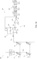
- figure 14 shows a different embodiment of the IMC device, here indicated by 400, wherein, differently from the IMC device 300 of figure 12 , the digital detectors, here indicated by 422, comprise each only the first integration circuit 334 and the first counter circuit 360. In practice, the digital detectors 422 of figure 14 do not comprise the switching circuit 336, the second integration circuit 335 and the second counter circuit 361 discussed with reference of figure 12 .
- each digital detector may be coupled to the respective bit line BL i differently from what shown and described here; for example, the integration stage 33 of figure 2 may be coupled to the bit line BLi without the current mirror 35, so that the integration stage 33 receives at the input node 36 directly the bit line current I BL,i .
- the integration stage 133 of the oscillator 120 may have the same circuit diagram as the integration stage 33, 330, 430 of any of the digital detectors 22, 322, 422, i.e. they may have equal circuit elements providing the integration signal and equal circuit elements providing the control signal from the integration signal.
- the integration stage of the oscillator and the digital detector may each have a first inverter and a capacitor providing the integration signal and a second inverter providing the control signal that is used by the respective counter stage.
- the capacitors of the integration stage of the digital detector and the capacitor of the integration stage of the oscillator may have the same capacitance value; and/or the first inverter of the integration stage of the digital detector may be equal to the first inverter of the integration stage of the oscillator; and/or the second inverter of the integration stage of the digital detector may be equal to the second inverter of the integration stage of the oscillator, e.g. having the same switching threshold.
- the integration stage of the oscillator and the digital detector may each have only one integration circuit (for example similarly to what discussed with reference to figure 14 ) or a first and a second integration circuit mutually coupled by a switching circuit.
- the memory cells 20 may be resistive memory cells not based on PCM materials, but on different technologies; for example, may be magnetoresistive (MRAM), resistive (RRAM) or static (SRAM) memory cells.
- MRAM magnetoresistive
- RRAM resistive
- SRAM static
- each memory cell 20 may be formed by a plurality of selectable resistive elements, equal or different from each other, mutually arranged in parallel, for example between the respective bit line and ground, that may be selectively enabled or disabled during programming of the memory array 12, so that the respective transconductance value g ij may be a multibit value.
- the oscillator may have the same circuit diagram as the digital detector of figure 12 or 14 .
- the charge counter stage 34 of the digital detectors 22 may comprise a second set of flip-flops, instead of the inverter 63, coupled to the second node 61 of the switching circuit 43, and a combination unit, similarly to what described with reference to figure 12 .
- the charge counter stage 137 of the oscillator 120 may comprise a second set of flip-flops, instead of the inverter 159, coupled to the second node 157 of the switching circuit 136, and a combination unit, similarly to what described with reference to figure 12 .
- the operational amplifiers 343 or 352 may be replaced by an inverter, as in the digital detectors 22 of figure 2 .
- the integration stage and the counter stage of the digital detectors may each be formed by a combination of the elements forming the digital detectors 22, 322 of figures 2 , 12 . Similar considerations apply, mutatis mutandis , to the integration stage and the counter stage of the oscillator, which, according to an embodiment, may have the same circuit diagram as the integration stage and counter stage of the digital detectors.
Landscapes
- Engineering & Computer Science (AREA)
- Physics & Mathematics (AREA)
- Theoretical Computer Science (AREA)
- General Physics & Mathematics (AREA)
- Mathematical Physics (AREA)
- Biomedical Technology (AREA)
- Life Sciences & Earth Sciences (AREA)
- Health & Medical Sciences (AREA)
- Data Mining & Analysis (AREA)
- Biophysics (AREA)
- Computing Systems (AREA)
- Software Systems (AREA)
- General Engineering & Computer Science (AREA)
- Mathematical Analysis (AREA)
- Neurology (AREA)
- Molecular Biology (AREA)
- Pure & Applied Mathematics (AREA)
- Mathematical Optimization (AREA)
- General Health & Medical Sciences (AREA)
- Computational Mathematics (AREA)
- Crystallography & Structural Chemistry (AREA)
- Chemical & Material Sciences (AREA)
- Artificial Intelligence (AREA)
- Computational Linguistics (AREA)
- Evolutionary Computation (AREA)
- Databases & Information Systems (AREA)
- Algebra (AREA)
- Computer Hardware Design (AREA)
- Analogue/Digital Conversion (AREA)
Abstract
Description
- The present invention relates to an in-memory computation device having an improved current reading circuit and to a control method.
- As is known, an in-memory computation device uses the specific arrangement of the memory cells of a memory array to perform an analogic data processing at the cell level.
- For example, in-memory computation devices are used to perform multiply and accumulate (MAC) operations, which are for example employed to implement machine learning algorithms, such as neural networks.
- A multiply and accumulate operation provides an output vector y1,...,yM as the multiplication of an input vector x1,...,xN by a vector or matrix of computational weights gij, e.g. :

- The in-memory computation device stores the computational weights gij in the cells of the memory and performs the multiplication and summation operations at the cell level.
- In detail, for each output vector yi, the known in-memory devices generate a current indicative of

- The in-memory computation devices allow to avoid back and forth transfer of data between a memory and an elaboration unit. Accordingly, the performance of an in-memory computation device is not limited by the data transfer bandwidth between memory and elaboration unit and has a low power consumption.
- However, the Applicant has verified that the ADCs of the known in-memory computation devices have a high die occupation area and a slow conversion time, thereby causing high manufacturing costs and low performances of the corresponding in-memory computation devices.
- The aim of the present invention is to overcome the disadvantages of the prior art.
- According to the present invention, an in-memory computation device and a control method thereof are provided, as defined in the attached claims.
- For a better understanding of the present invention, non-limiting embodiments are now described, with reference to the attached drawings, wherein:
-
figure 1 shows a block diagram of the present in-memory computation device, according to an embodiment; -
figure 2 shows a circuit diagram of a digital detector of the in-memory computation device offigure 1 , according to an embodiment; -
figure 3 shows a detailed circuit diagram of a portion of the digital detector offigure 2 ; -
figure 4 shows an example of waveforms of the digital detector offigure 2 , in use; -
figure 5 shows a block diagram of the present in-memory computation device, according to a different embodiment; -
figure 6 shows a circuit diagram of an oscillator of the in-memory computation device offigure 5 , according to an embodiment; -
figure 7 shows a detailed circuit diagram of a portion of the oscillator offigure 6 ; -
figure 8 shows a block diagram of a different portion of the in-memory computation device offigure 5 ; -
figure 9 shows an example of word line activation signals provided by the portion offigure 8 ; -
figure 10 shows a detailed circuit diagram of a portion of a digital detector of the in-memory computation device offigure 5 , according to an embodiment; -
figure 11 and12 show block diagrams of the present in-memory computation device, according to further embodiments; -
figure 13 shows an example of waveforms of a digital detector of the in-memory computation device offigure 12 , in use; and -
figure 14 shows a block diagram of the present in-memory computation device, according to a further embodiment. -
Figure 1 shows a circuit diagram of an in-memory computation device 10, hereinafter also referred to asIMC device 10, comprising a computation memory array (hereinafter indicated as memory array) 12, aline activation unit 14 and areading unit 16. - In
figure 1 , only the elements that are useful for understanding the present embodiment are shown, whereas elements and components that may be present in thefinal IMC device 10 and are not relevant for understanding the invention are not shown. - The
memory array 12 is of the non-volatile type and comprises a plurality ofmemory cells 20 organized in a matrix arrangement having M columns and N rows. - The
memory cells 20 arranged in the same column are mutually connected through a respective bit line BLi, wherein i=1,...,M. Thememory cells 20 arranged in the same row are mutually connected through a respective word line WLj, wherein j=1, ..., N . - In practice, a respective word line WLj and a respective bit line BLi are associated to each
memory cell 20. - The
memory cells 20 are programmed to store each a respective computational weight gij that may be used as a weight for performing an in-memory calculation. - The
line activation unit 14 provides a plurality of wordline activation signals 21, one for each word line WLj, that are configured to each activate thememory cells 20 of a respective word line WLj. - In this embodiment, the
line activation unit 14 receives an input vector X including a plurality of input values x1,...,xN, one for each word line WLj. The wordline activation signals 21 are pulses, in particular here rectangular pulses, each having a time width that is a function of the respective input value xj. - The
line activation unit 14 further receives an address signal ADR indicating which word lines WLj to activate for performing an in-memory calculation. For example, the address signal ADR may be used to cause the activation, in use, only of some of the plurality of word lines WL1, ..., WLN, for example if the input vector X has a number of values smaller than the number N of rows of thememory array 12. - The
reading unit 16 comprises a plurality ofdigital detectors 22 and abiasing circuit 24. - The
biasing circuit 24 provides a bias voltage Vr to the bit lines BL1, ..., BLM. - In this embodiment, the
biasing circuit 24 provides the same voltage Vr to all the bit lines BL1, ..., BLM. However, thebiasing circuit 24 may provide bias voltages different with each other to the bit lines BL1,...,BLM, depending on the specific application. - The
digital detectors 22 are each coupled to a respective bit line BLi and each provides an output signal yi indicative of a current IBL,i flowing through the respective bit line BLi, as discussed hereinafter in detail. - The
memory cells 20 each comprise astoring element 25 and aselection element 26. - The
storing element 25 of eachmemory cell 20 is a variable resistive element, in particular here based on a phase change material (PCM), such as a chalcogenide. - In detail, the computational weight gij indicates the transconductance value of the
storing element 25 of therespective memory cell 20, i.e. it is indicative of the programmed resistance of thestoring element 25. - A phase change material has at least two phase states, e.g. an amorphous phase and a crystalline phase, each having a respective resistivity.
- A phase change material may be transformed from one phase state to another by means of heat transfer, for example by using current pulses.
- The resistance of each
storing element 25 associated to the respective phase state is used to distinguish two or more logic states of thecorresponding memory cell 20. - For example, the amorphous phase may have a higher resistance than the crystalline phase. A logic state '0', or reset state, may be associated to the amorphous phase of the
storing element 25. A logic state '1', or set state, may be associated to the crystalline phase of the storingelement 25. - The storing
element 25 has a first terminal coupled to anode 28 of the respective bit line BLi and a second terminal coupled to a reference potential node, here toground 29, through theselection element 26. - The
selection element 26 is a switch, for example a BJT transistor, a diode or a MOS transistor, here an NMOS transistor, that is arranged in series with therespective storing element 25 and whose switching is controlled by the wordline activation signal 21 of the respective word line WLj. - In this embodiment, the NMOS transistor forming the
selection element 26 has a source coupled to, here directly connected to, theground 29; a drain coupled to, here directly connected to, the second terminal of thestoring element 25; and a gate coupled to, here directly connected to, the respective word line WLj. - In practice, the
storing element 25 and theselection element 26 form a current path of therespective memory cell 20; theselection element 26, in response to receiving therespective activation signal 21, closes the respective current path, thereby allowing the passage of a cell current icell from thecommon node 28 to theground 29. - The
IMC device 10 may further compriseinterface circuits 30 coupled to the bit lines BL1, ..., BLM that may be used, for example, to programme the transconductance values gij stored in thestoring elements 25, in a per se known way. - The
digital detectors 22 each comprise anintegration stage 33 and acounter stage 34 for each bit line BLi. - With reference to
figures 2 and3 , thedigital detectors 22 will be described hereinafter with respect to thedigital detector 22 coupled to a generic bit line BLi of the plurality of bit lines BL1,...,BLM. - In this embodiment, the
integration stage 33 comprises acurrent mirror 35 that mirrors the bit line current IBL,i of the bit line BLi into aninput node 36 of therespective integration stage 33. - The
current mirror 35 has a mirroring ratio 1:k, so that a mirrored bit line current k·IBL,i flows through theinput node 36 of theintegration stage 33. - In detail, the
current mirror 35 has a first branch, here formed by arespective PMOS transistor 37, coupled to the bit line BLi, and a second branch, here formed by arespective PMOS transistor 38, coupled to therespective integration stage 33. - The sources of the
PMOS transistors supply node 40, here at a voltage VDD, the gates of thePMOS transistors PMOS transistor 37. The drain of thePMOS transistor 38 is coupled to, in particular here is directly connected to, theinput node 36 of theintegration stage 33. - The
integration stage 33 comprises afirst integration circuit 41, asecond integration circuit 42, and aswitching circuit 43 coupled between the first and thesecond integration circuits - The first and the
second integration circuits input node 36 so as to receive the mirrored bit line current k·IBL,i. - The
first integration circuit 41 comprises afirst inverter 45 having anoutput 46, acapacitor 47 of capacitance CA coupled at theoutput 46 of thefirst inverter 45, and asecond inverter 48 whose input is coupled to theoutput 46 of thefirst inverter 45. - The
first inverter 45 has a supply node coupled to theinput node 36 of the integration stage 33 (figure 3 ) and receives at input a first control signal INA. - In practice, the
first inverter 45 is biased by the mirrored bit line current k·IBL,i. - The
capacitor 47 has a first terminal coupled to theoutput node 46 of thefirst inverter 45 and a second terminal coupled to a reference potential node, here to ground. - The
output node 46 of thefirst inverter 45 is at a first integration voltage VA that drops across thecapacitor 47. - The
second inverter 48 has a first sampling threshold, hereinafter referred to as first threshold Vth1, receives at input the first integration voltage VA and provides at output a first switch signal S1 as a function of the first threshold Vth1 and the first integration voltage VA. - In detail, the first switch signal S1 is a logic signal having a high logic value when the first integration voltage VA is smaller than the first threshold Vth1, and a low logic value when the first integration voltage VA is higher than the first threshold Vth1.
- The
second integration circuit 42 comprises afirst inverter 50 having anoutput 51, acapacitor 52 of capacitance CB coupled at theoutput 51 of thefirst inverter 50, and asecond inverter 53 whose input is coupled to theoutput 51 of thefirst inverter 50. - The
first inverter 50 has a supply node coupled to theinput node 36 of the integration stage 33 (figure 3 ) and receives at input a second control signal INB. - In practice, the
first inverter 50 is biased by the mirrored bit line current k·IBL,i. - The
capacitor 52 has a first terminal coupled to theoutput node 51 of thefirst inverter 50 and a second terminal coupled to a reference potential node, here to ground. - The
output node 51 of thefirst inverter 50 is at a second integration voltage VB dropping across thecapacitor 51. - The
second inverter 53 has a second sampling threshold Vth2, hereinafter referred to as second threshold Vth2, receives at input the second integration voltage VB and provides at output a second switch signal S2 as a function of the second threshold Vth2 and the second integration voltage VB. - In detail, the second switch signal S2 is a logic signal having a high logic value when the second integration voltage VB is smaller than the second threshold Vth2, and a low logic value when the second integration voltage VB is higher than the second threshold Vth2.
- In this embodiment, the first threshold Vth1 is equal to the second threshold Vth2; however, the first threshold Vth1 may be different to the second threshold Vth2, depending on the specific application.
- The switching
circuit 43 is a latch formed by twoinverters first switch 57 controlled by the first switch signal S1 and asecond switch 58 controlled by the second switch signal S2. - The switching
circuit 43 has afirst node 60 coupled to the input of theinverter 56 and the output of theinverter 55, and asecond node 61 coupled to the output of theinverter 56 and the input of theinverter 55. - The
first node 60 provides the first control signal INA. Thesecond node 61 provides the second control signal INB. - The
first switch 57 is coupled between thefirst node 60 and a node at a voltage V'DD, thesecond switch 58 is coupled between thesecond node 61 and the node at the voltage V'DD. - The voltage V'DD may be equal or different to the voltage VDD of the
supply node 40. For example, if the voltage V'DD is different, in particular smaller, than the voltage VDD, thedigital detector 22 may comprise a voltage scaling circuit, for example a transistor, here not shown, whose source and drain terminals are coupled between thesupply node 40 and theinput node 36 of theintegration stage 33. - In this embodiment, the switching
circuit 43 also receives an enable signal EN, which controls the activation of the switchingcircuit 43. For example, the enable signal EN may be used to keep the switchingcircuit 43 off when not in use, thereby allowing to optimize power consumption. In addition, the enable signal EN may be used to set the switchingcircuit 43 in a defined state, for example upon turning on of theIMC device 10. - The
charge counter stage 34 is coupled to the first and thesecond nodes circuit 43. - In detail, the
charge counter stage 34 comprises aninverter 63, whose input is coupled to thesecond node 61, and a counter comprising aninverter 65 whose input is coupled to thefirst node 60 and a plurality of D flip-flops 67 including a first flip-flop 67.2, a second flip-flop 67.3 and a last flip-flop 67.F, wherein F is the number of bits of the output signal yi. In practice, the counter of thecharge counter stage 34 has F-1 flip-flops 67. - The output of the
inverter 63 provides the first bit yi(1), i.e. the least significant bit, of the output signal yi. - In other words, the output of the
inverter 63 may be used, at the end of a calculation performed by theIMC device 10, as the least significant bit yi(1) of the output signal yi. - The flip-
flops 67 are cascaded one with the other, in sequence from the first flip-flop 67.2 to the last flip-flop 67.F. - The flip-
flops 67 each have a clock input (CK-input), a data input (D-input), a Q-output, and aQ -output. - The CK-input of the first flip-flop 67.2 is coupled to the output of the
inverter 65. TheQ -output of the first flip-flop 67.2 is fed back to the D-input of the first flip-flop 67.2. The Q-output of the first flip-flop 67.2 forms the second bit yi(2) of the output signal yi. - The CK-input of the second flip-flop 67.3 is coupled to the
Q -output of the first flip-flop 67.2. TheQ -output of the second flip-flop 67.3 is fed back to the D-input of the second flip-flop 67.3. The Q-output of the second flip-flop 67.3 forms the third bit yi(2) of the output signal yi. - What described for the second flip-flop 67.3 applies, mutatis mutandis, to all the subsequent flip-flops, here not shown, up to the F-1-th flip-flop, also not shown.
- Finally, the CK-input of the last flip-flop 67.F is coupled to the
Q -output of the F-1-th flip-flop. TheQ- output of the last flip-flop 67.F is fed back to the D-input of the last flip-flop 67.F. The Q-output of the last flip-flop 67.F forms the most significant bit yi(F) of the output signal yi. - With reference to the detailed implementation of the
integration stage 33 shown infigure 3 , thefirst inverter 45 of thefirst integration circuit 41 is a CMOS inverter formed by the series circuit of aPMOS transistor 70 and anNMOS transistor 71, mutually coupled at theoutput node 46. The PMOS andNMOS transistors - The source of the
PMOS transistor 70 is coupled to theinput node 36 of theintegration stage 33. - The
second inverter 48 of thefirst integration circuit 41 is a CMOS inverter formed by the series circuit of aPMOS transistor 72 and anNMOS transistor 73, mutually coupled at anode 74 providing the first switch signal S1. - The first threshold Vth1 of the
second inverter 48 is the switching threshold of thesecond inverter 48, and therefore depends on the properties, for example the threshold or the on-resistance, of the PMOS andNMOS transistors - For example, the switching threshold of the
second inverter 48 may be defined as the operating point at which the respective input voltage, i.e. the first integration voltage VA, is equal to the respective output voltage, i.e. the first switch signal S1. - The
first inverter 50 of thesecond integration circuit 42 is a CMOS inverter formed by the series circuit of aPMOS transistor 75 and anNMOS transistor 76, mutually coupled at theoutput node 51. The PMOS andNMOS transistors - The source of the
PMOS transistor 75 is coupled to theinput node 36 of theintegration stage 33. - The
second inverter 53 of thesecond integration circuit 42 is a CMOS inverter formed by the series circuit of aPMOS transistor 77 and anNMOS transistor 78, mutually coupled at anode 79 providing the second switch signal S2. - The second threshold Vth2 of the
second inverter 53 is the switching threshold of thesecond inverter 53, i.e. depends on the properties of the PMOS andNMOS transistors NMOS transistors - As shown in the detailed implementation of
figure 3 , the first and thesecond inverters circuit 43 are cross-coupled CMOS inverters each comprising arespective PMOS transistor 80 and arespective NMOS transistor 81 mutually coupled in series between a supply node, here at the voltage V'DD, and ground. - Moreover, the first and the
second inverters circuit 43 also comprise each a respective enabling switch, here aPMOS transistor 82, that is coupled between the supply node at the voltage V'DD and thePMOS transistor 80 of the respective inverter. - The
PMOS transistors 82 are controlled by the enabling signal EN. - In use, the bit line current IBL,i of the bit line BLi is mirrored into the
integration stage 33 of the respectivedigital detector 22. -
Figure 4 shows an example of the time behaviour of the first control signal INA, the first integration voltage VA and the second integration voltage VB of thedigital detector 22 offigure 2 . - For t0<t<t1, the first integration voltage VA is below the first threshold Vth,1. Accordingly, the
PMOS transistor 72 of thesecond inverter 48 is on and theNMOS transistor 73 of thesecond inverter 48 is off. Therefore, the first switch signal S1 (here not shown) has the high value and thefirst switch 57 is open. The first control signal INA has the low value. - It follows that, with respect to the
first inverter 45 of thefirst integration circuit 41, for t0<t<t1, thePMOS transistor 70 is on and theNMOS transistor 71 is off. - At the same time, for t0<t<t1, the second control signal INB has the high value. Therefore, with respect to the
first inverter 50 of thesecond integration circuit 42, for t0<t<t1, thePMOS transistor 75 is off and theNMOS transistor 76 is on. - Accordingly, the mirrored bit line current k·IBL,i flows, from the
input node 36, only through thefirst inverter 45 of thefirst integration circuit 41 and not through thefirst inverter 50 of thesecond integration circuit 42. - In detail, the mirrored bit line current k·IBL,i flows through the
PMOS transistor 70 and charges thecapacitor 47. The first integration voltage VA thus increases in time for t0<t<t1. - In detail, in the example of
figure 4 , the first integration voltage VA increases linearly in time for t0<t<t1; however, the behaviour of the first integration voltage VA depends on the specific behaviour of the bit line current IBL,i in the time interval t0<t<t1. - When the first integration voltage VA becomes equal to the first threshold voltage Vth,1, the
NMOS transistor 73 of thesecond inverter 48 turns on and thePMOS transistor 72 turns off. - In this embodiment, the first control signal INA assumes the high value at a time instant t2.
- The time delay between instants t1 and t2 may correspond, for example, to the propagation delay of the
second inverter 48 of thefirst integration circuit 41 and/or the switching time of thefirst switch 57. - For t1<t<t2, the mirrored bit line current IBL,i keeps charging the
capacitor 47; accordingly, the first integration voltage VA increases up to a maximum value (instant t2). - At the time instant t2, when the first control signal INA assumes the high value, the second control signal INB (here not shown) assumes the low value (the
inverter 56 of the switchingcircuit 43 receives the first control signal INA at input). - While the first control signal INA has the high value, the
PMOS transistor 70 and theNMOS transistor 71 of thefirst inverter 45 of thefirst integration circuit 41 are off and, respectively, on. At the same time, while the second control signal INB has the low value, thePMOS transistor 75 and theNMOS transistor 76 of thefirst inverter 50 of thesecond integration circuit 42 are on and, respectively, off. - Therefore, for t>t2, the mirrored bit line current k·IBL,i flows, from the
input node 36, only through thefirst inverter 50 of thesecond integration circuit 42 and not through thefirst inverter 45 of thefirst integration circuit 41. - In detail, the mirrored bit line current k·IBL,i flows through the
PMOS transistor 75 and charges thecapacitor 52 of thesecond integration circuit 42. The second integration voltage VB thus increases in time from the time instant t2. - In detail, in the example of
figure 4 , the second integration voltage VB increases linearly in time for t>t2; however, the behaviour of the second integration voltage VB depends on the specific behaviour of the bit line current IBL,i. - While the first control signal INA has the high value, the
capacitor 47 of thefirst integration circuit 41 discharges through theNMOS transistor 71 of thefirst inverter 45. The first integration voltage VA thus decreases to zero. - When the second integration voltage VB becomes equal to the second threshold voltage Vth,2 (time instant t3), the
NMOS transistor 78 of thesecond inverter 53 turns on and thePMOS transistor 77 turns off. - Accordingly, at a time instant t4, the second control signal INB assumes the high value, similarly to what has been discussed above for the first control signal INA in correspondence of time instant t2.
- In detail, in response to the second integration voltage VB reaching the second threshold Vth,2, the second switch signal S2 switches to the low value and the
second switch 58 closes, so that thesecond node 61 is at the voltage V'DD and, accordingly, the second control signal INB assumes the high value. - The time delay between instants t3 and t4 may correspond, for example, to the propagation delay of the
second inverter 53 of thesecond integration circuit 42 and/or the switching time of thesecond switch 58. - For t3<t<t4, the mirrored bit line current k·IBL,i keeps charging the
capacitor 52 of thesecond integration circuit 42; accordingly, the second integration voltage VB increases up to a maximum value (instant t4). - For t2<t<t4, the switching
circuit 43 keeps the first control signal INA at the high value and the second control signal INB at the low value. - At the time instant t4, the first control signal INA assumes the low value again, in response to the second control signal INB assuming the high value.
- In response to the first control signal INA assuming the low value, the mirrored bit line current k·IBL,i returns to charging the
capacitor 47 of thefirst integration circuit 41 up to a time instant t6, similarly to what has been discussed for t1<t<t2. - Consequently, from time instant t6 to time instant t7, the mirrored bit line current k·IBL,i charges the
capacitor 52 of thesecond integration circuit 42 up to a time instant t7, similarly to what has been discussed for t2<t<t4. - Again with reference to
figure 2 , thecounter stage 34, in particular the flip-flops 67, counts the number of switching events of the first control signal INA, in particular in this embodiment counts the number of rising edges of the first control signal INA. - In practice, the
digital detectors 22 each measure the bit line current IBL,i of the respective bit line BLi by performing a number of successive sampling iterations. In each sampling iteration, for example with respect to a sampling iteration wherein the mirrored bit line current k·IBL,i flows through thefirst integration circuit 41, theintegration stage 33 generates the first integration voltage VA as the time integral of the mirrored bit line current k·IBL,i, compares the first integration voltage VA with the first threshold Vth,1 and, in response to the first integration voltage VA reaching the first threshold Vth,1, resets the first integration voltage VA, in particular here by switching the first control signal INA. Thecounter stage 34 updates the respective output signal yi in response to the first integration voltage VA reaching the first threshold Vth,1. - In this embodiment, the least significant bit of the output signal yi is the value of the second control signal INB at the end of the computation performed by the
IMC device 10. - In other words, the
digital detectors 22 sample each the respective bit line current IBL,i by converting the bit line current IBL,i into a number of charge packets and counting said charge packets, wherein each charge packet corresponds to the charge accumulated on thecapacitors second inverters - It follows that the
capacitors capacitors factor 2F, wherein F is the number of bits of the output signal yi. - Therefore, the
digital detectors 22 may have a low die area occupancy and, accordingly, theIMC device 10 may have low manufacturing costs. - In addition, the
digital detectors 22 each start discretizing the respective bit line current IBL,i while the bit line current IBL,i flows through the respective bit line BLi. Therefore, the output signal yi may be ready soon after an end of a computation performed by theIMC device 10 or soon after the respective bit line current IBL,i stops. - For example, according to an embodiment, the
digital detectors 22 may sample each the respective bit line current IBL,i until thedigital detectors 22 receive a stop signal, for example from a user of theIMC device 10 or from the wordline activation unit 14, indicating the end of the computation performed by theIMC device 10. - Therefore, the
digital detectors 22 may have a fast measurement time, thereby allowing theIMC device 10 to have a low computation time. - Moreover, according to the illustrated embodiment, the switching
circuit 43 disables thefirst integration circuit 41 and enables thesecond integration circuit 42, in response to the first integration signal VA reaching the first threshold Vth,1, and enables thefirst integration circuit 41 and disables thesecond integration circuit 42, in response to the second integration signal VB reaching the second threshold Vth,2. - This allows the bit line current IBL,i to be sampled alternatively by the
first integration circuit 41 and thesecond integration circuit 42, thereby allowing the bit line current IBL,i to charge thecapacitor 47 while thecapacitor 52 is discharging, and to charge thecapacitor 52 while thecapacitor 47 is discharging. By doing so, no charge may be lost during the sampling and thedigital detector 22 may achieve a high measurement accuracy of the bit line current IBL,i. - The
IMC device 10 may be used to perform a multiply and accumulate (MAC) operation, in particular between the input vector X=x1,...,xN and the matrix formed by the computational weights gij. - In fact, the cell current icell that each
memory cell 20 sinks, here from therespective node 28 to ground 29 depends on the transconductance gij of therespective storing element 25 and the activation time of therespective selection element 26, i.e. on the pulse length of the respective wordline activation signal 21. - In detail, the absolute value of each cell current icell depends on the respective transconductance value gij. The time duration of each cell current icell depends on the respective activation time.
- Accordingly, an electric charge may be associated to each cell current icell; said electric charge is a function of the respective transconductance value gij and the respective activation time.
- Since the pulse length of the word line activation signals 21 is a function of the respective input value xj, the electric charge associated to each cell current icell is a function of the product gij·xj.
- For each bit line BLi, the respective bit line current IBL,i is a summation of the cell currents icell. Therefore, the total electric charge associated to each bit line current IBL,i is a function of the multiply and accumulate operation gi1·x1 + gi2·x2 + ... + giN·xN.
- Accordingly, each output signal yi, which is obtained by measuring the respective bit line current IBL,i, in particular by integrating the respective bit line current IBL,i, is indicative of the MAC operation gi1·x1 + gi2·x2 + ... + giN·xN.
-
Figure 5 shows a different embodiment of the present IMC device, here indicated by 100. TheIMC device 100 has a general structure similar to IMC device offigure 1 ; therefore, elements in common are indicated by the same reference numbers and are not further described in detail. - The
IMC device 100 comprises thememory array 12, here shown only in part, aline activation unit 114 and thereading unit 16. - The
memory array 12 comprises thememory cells 20 each coupled to a respective bit line BLi, with i=1,...,M, and a respective word line WLj, with j=1,...,N. - The
reading unit 16 comprises also here the biasingcircuit 24 and thedigital detectors 22. - The word
line activation unit 114 receives the input signal X including the plurality of input values x1,...,xN, and provides the plurality of word line activation signals 21 each as a function of a respective input value xj. - In detail, the
line activation circuit 114 comprises anoscillator 120 providing a timer signal TM<L:1> having L bits, and a plurality ofcomparators 122, one for each word line WL1,...,WLN. The plurality ofcomparators 122 receive each the timer signal TM<L:1> and a respective input value xj and, in response, provide a respective wordline activation signal 21. - The
oscillator 120, shown in detail infigures 6 and7 , comprises acurrent generation portion 125 generating an oscillator current, here a mirrored current p·IOSC, and acounting portion 126 that generates the timer signal TM<L:1> from the oscillator current. - In detail, the
current generation portion 125 comprises acurrent source 127 generating a supply current IOSC and acurrent mirror 128 that mirrors the supply current IOSC into aninput node 129 of the countingportion 126. - The supply current IOSC may be for example equal to a maximum current that may flow through a bit line BLi, i.e. the current that flows in the bit line BLi when all the
memory cells 20 associated to the bit line BLi are activated. - Alternatively, the supply current IOSC may have a different value, depending on the specific application.
- The
current mirror 128 has a mirroring ratio 1:p, so that the mirrored current that flows through theinput node 129 of the countingportion 126 is p·IOSC. - In detail, the
current mirror 128 has a first branch, here formed by arespective PMOS transistor 130, coupled to thecurrent source 127, and a second branch, here formed by arespective PMOS transistor 131, coupled to the countingportion 126. - The sources of the
PMOS transistors supply node 132, here at the voltage VDD, the gates of thePMOS transistors PMOS transistor 130. The drain of thePMOS transistor 131 is coupled to, in particular here is directly connected to, theinput node 129 of the countingportion 126. - The counting
portion 126 of theoscillator 120 comprises anintegration stage 133, formed here by afirst integration circuit 134, asecond integration circuit 135 and aswitching circuit 136 coupled between the first and thesecond integration circuits counter stage 137 which is coupled to theintegration stage 133 and provides the timer signal TM<L:1>. - The first and the
second integration circuits input node 129 so as to receive the mirrored current p·IOSC. - The
first integration circuit 134 comprises afirst inverter 140 having anoutput 141, acapacitor 142 of capacitance C'A coupled at theoutput 141 of thefirst inverter 140, and asecond inverter 143 whose input is coupled to theoutput 141 of thefirst inverter 140. - The
first inverter 140 has a supply node coupled to theinput node 129 of the counting portion 126 (figure 7 ) and receives at input a first oscillator control signal OSA. - In practice, the
first inverter 140 is biased by the mirrored current p·IOSC. - The
capacitor 142 has a first terminal coupled to theoutput node 141 of thefirst inverter 140 and a second terminal coupled to a reference potential node, here to ground. - The
output node 141 of thefirst inverter 140 is at a first oscillator integration voltage V'A that drops across thecapacitor 142. - The
second inverter 143 has a first oscillator threshold V'th1, hereinafter simply referred to as first threshold V'th,1, receives at input the first oscillator integration voltage V'A and provides at output a first oscillator switch signal S'1 as a function of the first threshold V'th1 and the first oscillator integration voltage V'A. - In detail, when the first oscillator integration voltage V'A is smaller than the first threshold V'th1, the first oscillator switch signal S'1 has a high logic value. When the first oscillator integration voltage V'A is higher than the first threshold V'th1, the first oscillator switch signal S'1 has a low logic value.
- The
second integration circuit 135 comprises afirst inverter 146 having anoutput 147, acapacitor 148 of capacitance C'B coupled at theoutput 147 of thefirst inverter 146, and asecond inverter 149 whose input is coupled to theoutput 147 of thefirst inverter 146. - The
first inverter 146 has a supply node coupled to theinput node 129 of the counting portion 126 (figure 7 ) and receives at input a second oscillator control signal OSB. - In practice, the
first inverter 146 is biased by the mirrored current p·IOSC. - The
capacitor 148 has a first terminal coupled to theoutput node 147 of thefirst inverter 146 and a second terminal coupled to a reference potential node, here to ground. - The
output node 147 of thefirst inverter 146 is at a second oscillator integration voltage V'B dropping across thecapacitor 148. - The
second inverter 149 has a second oscillator threshold V'th2, hereinafter simply referred to as second threshold V'th,2, receives at input the second oscillator integration voltage V'B and provides at output a second oscillator switch signal S'2 as a function of the second threshold V'th2 and the second oscillator integration voltage VB. - In detail, when the second oscillator integration voltage VB is smaller than the second threshold V'th2, the second oscillator switch signal S'2 has a high logic value. When the second oscillator integration voltage V'B is higher than the second threshold V'th2, the second oscillator switch signal S'2 has a low logic value.
- In this embodiment, the first threshold V'th1 of the
second inverter 143 is equal to the first threshold Vth1 of thesecond inverter 48 of the digital detectors 22 (figures 2 and3 ). The second threshold V'th2 of thesecond inverter 146 is equal to the second threshold Vth2 of thesecond inverter 53 of the digital detectors 22 (figures 2 and3 ). - Again with reference to
figure 6 , theswitching circuit 136 is a latch formed by twoinverters first switch 153 controlled by the first oscillator switch signal S'1 and asecond switch 154 controlled by the second oscillator switch signal S'2. - The
switching circuit 136 has afirst node 156 coupled to the input of theinverter 151 and the output of theinverter 150, and asecond node 157 coupled to the output of theinverter 151 and the input of theinverter 150. - The
first node 156 provides the first oscillator control signal OSA. Thesecond node 157 provides the second oscillator control signal OSB. - The
first switch 153 is coupled between thefirst node 156 and a node at the voltage V'DD, thesecond switch 154 is coupled between thesecond node 157 and the node at the voltage V'DD. - According to an embodiment, the voltage V'DD of the counting
portion 126 of theoscillator 120 may be equal to the voltage V'DD of theintegration stage 33 of the digital detector 22 (figure 2 ). - In the embodiment of
figure 6 , theswitching circuit 136 also receives an oscillator enable signal EN', which controls the activation of theswitching circuit 136. For example, the oscillator enable signal EN' may be used to keep the switchingcircuit 136 off when not in use, thereby allowing to optimize power consumption. In addition, the enable signal EN' may be used to set theswitching circuit 136 in a defined state, for example upon turning on of theIMC device 10. Thecounter stage 137 is coupled to the first and thesecond nodes switching circuit 136. - In detail, the
charge counter stage 137 comprises aninverter 159, whose input is coupled to thesecond node 157, and a counter comprising aninverter 160 whose input is coupled to thefirst node 156 and a plurality of D flip-flops 161 including a first flip-flop 161.2, a second flip-flop 161.3 and a last flip-flop 161.L, wherein L is the number of bits of the timer signal TM<L:1>. In practice, the counter of thecharge counter stage 137 has L-1 flip-flops 161. - The output of the
inverter 159 provides the first bit TM(1), i.e. the least significant bit, of the timer signal TM. - The flip-
flops 161 are cascaded one with the other, in sequence from the first flip 161.2 to the last flip-flop 161.L. - The flip-
flops 161 each have a clock input (CK-input), a data input (D-input), a Q-output, and aQ -output. - The CK-input of the first flip-flop 161.2 is coupled to the output of the
inverter 160. TheQ -output of the first flip-flop 161.2 is fed back to the D-input of the first flip-flop 161.2. The Q-output of the first flip-flop 161.2 forms the second bit TM(2) of the timer signal TM<L:1>. - The CK-input of the second flip-flop 161.3 is coupled to the
Q -output of the first flip-flop 161.2. TheQ -output of the second flip-flop 161.3 is fed back to the D-input of the second flip-flop 161.3. The Q-output of the second flip-flop 161.3 forms the third bit TM(3) of the timer signal TM<L:1>. - What described for the second flip-flop 161.3 applies, mutatis mutandis, to all the subsequent flip-flops, here not shown, up to the L-1-th flip-flop, also not shown.
- Finally, the CK-input of the last flip-flop 161.L is coupled to the
Q -output of the L-1-th flip-flop. TheQ- output of the last flip-flop 161.L is fed back to the D-input of the last flip-flop 161.L. The Q-output of the last flip-flop 161.L forms the most significant bit TM(L) of the timer signal TM<L:1>. - With reference to the detailed implementation of the
integration stage 133 shown infigure 7 , thefirst inverter 140 of thefirst integration circuit 134 is a CMOS inverter formed by the series circuit of aPMOS transistor 165 and an NMOS transistor 166, mutually coupled at theoutput node 141. The PMOS andNMOS transistors 165, 166 receive the first oscillator control signal OSA at the respective gate terminals. - The source of the
PMOS transistor 165 is coupled to theinput node 129 of theintegration stage 133 of theoscillator 120. - The
second inverter 143 of thefirst integration circuit 134 is a CMOS inverter formed by the series circuit of aPMOS transistor 168 and anNMOS transistor 169, mutually coupled at anode 170 providing the first oscillator switch signal S'1. - The first threshold V'th1 of the
second inverter 143 is the switching threshold of thesecond inverter 143, and therefore depends on the properties, for example the threshold or the on-resistance, of the PMOS andNMOS transistors - For example, the switching threshold of the
second inverter 143 may be defined as the operating point at which the respective input voltage, i.e. the first oscillator integration voltage V'A, is equal to the respective output voltage, i.e. the first oscillator switch signal S'1. - The
first inverter 146 of thesecond integration circuit 135 is a CMOS inverter formed by the series circuit of aPMOS transistor 171 and anNMOS transistor 172, mutually coupled at theoutput node 173. The PMOS andNMOS transistors - The source of the
PMOS transistor 171 is coupled to theinput node 129 of the countingportion 126 of theoscillator 120. - The
second inverter 149 of thesecond integration circuit 135 is a CMOS inverter formed by the series circuit of aPMOS transistor 175 and anNMOS transistor 176, mutually coupled at anode 177 providing the second oscillator switch signal S'2. - The second threshold V'th2 of the
second inverter 149 is the switching threshold of thesecond inverter 149, and therefore depends on the properties, for example the threshold or the on-resistance, of the PMOS andNMOS transistors - For example, the switching threshold of the
second inverter 149 may be defined as the operating point at which the respective input voltage, i.e. the second oscillator integration voltage V'B, is equal to the respective output voltage, i.e. the second oscillator switch signal S'2. - As shown in the detailed implementation of
figure 7 , the first and thesecond inverters switching circuit 136 are cross-coupled CMOS inverters each comprising arespective PMOS transistor 180 and arespective NMOS transistor 181 mutually coupled in series between a supply node, here at the voltage V'DD, and ground. - Moreover, the first and the
second inverters switching circuit 136 also comprise each a respective enabling switch, here aPMOS transistor 182, that is coupled between the supply node at the voltage V'DD and thePMOS transistor 180 of the respective inverter. - The
PMOS transistors 182 are controlled by the oscillator enabling signal EN'. - In practice, in this embodiment, the
oscillator 120, in particular therespective integration stage 133, has a circuit diagram that is equal to the circuit diagram of any one of thedigital detectors 22 offigures 2 and3 , in particular of therespective integration stage 33. - It follows that the
oscillator 120 generates the timer signal TM<L:1> from the oscillator current IOSC in the same way as any one of thedigital detectors 22 generates the output signal yi from the respective bit line current IBL,i. - Thus, the
oscillator 120 generates the timer signal TM<L:1> by performing a number of successive timing iterations. In each timing iteration, for example with respect to a timing iteration wherein the mirrored oscillator current p·IOSC flows through thefirst integration circuit 134, theintegration stage 133 generates the first integration oscillation voltage V'A as the time integral of the mirrored oscillator current p·IOSC, compares the first oscillator integration voltage V'A with the first threshold V'th,1 and, in response to the first oscillator integration voltage V'A reaching the first threshold V'th,1, resets the first oscillator integration voltage V'A, in particular here by switching the first oscillator control signal OSA. Thecounter stage 137 updates the timer signal TM<L:1> in response to the first oscillator integration voltage V'A reaching the first threshold V'th,1. - In this embodiment, the least significant bit of the timer signal TM is the value of the second oscillator control signal OSB.
- In other words, the
oscillator 120 samples the oscillator current IOSC by converting the oscillator current IOSC into a number of charge packets and counting said charge packets, wherein each charge packet corresponds to the charge accumulated on thecapacitors second inverters - It follows that the timer signal TM<L:1> is updated at a frequency fu given by the switching events of the first oscillator control signal OSA (similarly to what discussed for the first control signal INA with reference to
figure 4 ). The update frequency fu thus depends on the value of the oscillator current IOSC, the mirror factor p of thecurrent mirror 128, the capacitances C'A, C'B, and the first and second thresholds V'th,1, V'th,2 of thesecond inverters -
Figure 8 shows in detail an embodiment of the input-time converter 122 of a word line WLj of the plurality of word lines WL1,...,WLM comprising acomparator 190 receiving the timer signal TM<L:1> and the respective input value xj and providing, in response, a match signal MTC; and a pulse generation circuit, here formed by aNAND logic gate 191 and aninverter 192, providing the respective wordline activation signal 21. - In this embodiment, the input value xj and the timer signal TM<L:1> are digital signals.
- The
comparator 190, for example a bit checking circuit based on a XOR logic gate, compares the input value xj and the timer signal TM<L:1> and asserts the match signal MTC to the high logic value when the timer signal TM<L:1> becomes equal to the input value xj. - The
NAND logic gate 191 receives the match signal MTC and an address enable signal ADR_EN indicating if the word line WLj has to be activated during the performance of an in-memory calculation. In detail, the address enable signal ADR_EN may have a high logic value if the word line WLj has to be activated during the in-memory calculation. - The
inverter 192 is coupled at input to the output of theNAND logic gate 191 and provides at output the wordline activation signal 21. In practice, theinverter 192 operates as a driver circuit for the respective word line WLj. - With respect to word line WLj, the input-
time converter 122 keeps the respective wordline activation signal 21 to the high logic value (i.e. thereby here activating theselection elements 26 of thememory cells 20 coupled to the word line WLj) as long as the timer signal TM<L:1> is different from the input value xj. - Therefore, the word line activation signals 21 each have a respective activation length Tj that is proportional to the update frequency fu of the timer signal TM<L:1> and the respective input value xj.
-
Figure 9 shows, by way of example, the word line activation signals 21 of the first word line WL1 and the last word line WLN. At the beginning of a computation by the IMC device 100 (instant t0) the timer signal TM<L:1> of theoscillator 120 is reset to a start value, for example to zero, and the input-time converters 122 switch each the respective wordline activation signal 21 to the high value. - In the example of
figure 9 , the input value x1 associated to the first word line WL1 is smaller than the input value xN associated to the last word line WLN; therefore, the input-time converter 122 associated to the first word line WL1 keeps the respective wordline activation signal 21 to the high value for a time shorter with respect to the input-time converter 122 associated to the last word line WLN. This results in the wordline activation signal 21 of the first word line WL1 having an activation length T1 that is smaller than the activation length TN of the wordline activation signal 21 of the last word line WLN. - In use, the fact that the
oscillator 120 generates the timer signal TM<L:1> from the oscillator current IOSC in the same way as thedigital detectors 22 each generate the respective output signal yi from the respective bit line current IBL,i, in particular the fact that therespective integration circuits - Therefore, global variations that may affect the
IMC device 100, such as drifts of the supply voltages VDD, V'DD and/or temperature variations, are compensated by theoscillator 120 and thedigital detectors 22, without thereby affecting the precision of the MAC operation performed by theIMC device 100. - According to an embodiment, the
oscillator 120 may comprise a computation-end comparator 193, as indicated by a dashed line infigure 5 . - The computation-
end comparator 193 receives the timer signal TM<L:1> and a max count signal MAX_COUNT<L:1> and provides, in response, an end-count signal END. - The max count signal MAX_COUNT<L:1> may be received from a user of the
IMC device 10 and indicates the maximum duration of a calculation performed by theIMC device 10. For example, the max count signal MAX_COUNT<L:1> may indicate a maximum duration equal to or higher than the time that any of the output signals yi would take to reach the maximum value, e.g. all F bits equal to 1, when all thecells 20 associated to the bit line BLi are activated. However, the max count signal MAX_COUNT<L:1> may indicate a smaller maximum duration, for example if it is desired to obtain a shorter computation time by theIMC device 10. - In this case, the
oscillator 120 may comprise, with reference tofigure 7 , a first and a second stop switches, here a first and asecond NMOS transistors oscillator 120 from updating the timer signal TM. - In detail, the first and the
second NMOS transistors output nodes second integration circuits second NMOS transistors - When the timer signal TM<L:1> becomes equal to the max count signal MAX_CNT<L:1>, the end-
computation comparator 195 switches the end signal END to the high logic value, thereby turning on the first and thesecond NMOS transistors output nodes second integration circuits - Consequently, the
oscillator 120 stops updating the timer signal TM. -
Figure 10 shows a different embodiment of the integration stage of any of thedigital detectors 22 of thereading unit 16, here indicated asintegration stage 220. Theintegration stage 220 differs from theintegration stage 33 shown infigure 3 in that it comprises a first and a second stop switches, here a first and asecond NMOS transistors digital detectors 22 from measuring the respective bit line current IBL,i. - In detail, the first and the
second NMOS transistors output nodes second integration circuits second NMOS transistors - When the timer signal TM<L:1> becomes equal to the max count signal MAX_CNT<L:1>, the end-
computation comparator 193 switches the end signal END to the high logic value, thereby turning on the first and thesecond NMOS transistors output nodes second integration circuits - Consequently, the first and the
second integration circuits - In practice, the end-count signal END may be used to determine the end of the MAC calculation by the
IMC device 100. -
Figure 11 shows a further embodiment of the present IMC device, here indicated by 200. TheIMC device 200 has a general structure similar to theIMC device 100 offigure 5 ; therefore, elements in common are indicated by the same reference numbers and not further described. - In detail, the
IMC device 200 comprises thememory array 12, thereading unit 16 and the wordline activation unit 114. - The
reading unit 16 comprises the plurality ofdigital detectors 22, one for each bit line BLi. - The word
line activation unit 114 comprises theoscillator 120 and the input-time converters 122 providing the word line activation signals 21. - The
IMC device 200 further comprises areference memory array 205 comprising one or more reference cells, here a plurality ofreference cells 206, of the non-volatile type. - The
reference memory array 205 may be a portion of thememory array 12 or may be a separate memory array. - The
reference cells 206 have the same circuit configuration as thememory cells 20 of thememory array 12. - In detail, the
reference cells 206 comprise each a storingelement 210 and aselection element 211, in particular equal to the storingelement 25 and, respectively, theselection element 26 of thememory cells 20. - In practice, the storing
element 210 is based on the same technology that is used to obtain the storingelement 25. For example, if the storingelement 25 is based on a PCM material, then the storingelement 210 is also based on a PCM material, in particular the same PCM material. - The
reference cells 206 are programmed to store respective reference transconductance values, which may be equal or different to one another, depending on the specific application. - The number of
reference cells 206 and the respective reference transconductance values may be chosen, at the design stage, so that thereference memory array 205 is a statistically significant sample of thememory array 12. - In practice, the
reference memory array 205 has an overall reference transconductance value gref that statistically represents an overall transconductance of thememory array 12. - For example, the overall transconductance of the
memory array 12 may be equal to the transconductance that thememory array 12 would have if all thereference cells 20 are activated at the same time. - For example, the number of
reference cells 206 may be higher than one hundred. - For example, the
reference cells 206 may be programmed so that the overall transconductance gref of thereference memory array 205 is equal to a mean value of the overall transconductance of thememory array 12. - For example, the mean value may represent the average transconductance value that the
memory array 12 has in use, for example as determined during a calibration or initialization step of theIMC device 10. - The storing
elements 210 have a first terminal that is coupled to acommon node 213 and a second terminal coupled to a reference potential node, here to ground 29, through theselection element 211. - In practice, the
reference cells 206 all share a same reference bit line BLref. - The
selection elements 211 are each formed by a respective switch, here an NMOS transistor, that is arranged in series with therespective storing element 210. - In this embodiment, the
selection elements 211 of all thereference cells 206 are controlled by a same reference activation signal REF, which for example may be generated by the wordline activation unit 114 or by other components of theIMC device 200, here not shown. - However, the
selection elements 211 may be controlled each by a respective reference activation signal, different one from the other, depending on the number ofreference cells 206 that is intended to activate. - For example, the reference activation signal REF may keep all the
reference memory cells 206 activated for the whole duration of a computation performed by theIMC device 10. - In this embodiment, with reference to the implementation of the
oscillator 120 offigure 6 , thereference memory array 205 forms thecurrent source 127. - In detail, the
common node 213 of thereference memory array 205 is coupled to the first branch of thecurrent mirror 128, in particular to the drain of thePMOS transistor 130. - In practice, in use, the
reference memory array 205 is biased by a fixed voltage, here the voltage VDD of thesupply node 132, but the oscillator current IOSC depends on the transconductance values of thereference cells 206. - In use, the
IMC device 200 may be subject to a temperature variation that may affect the transconductance values gij of thememory cells 20. Moreover, the transconductance values gij of thememory cells 20 may be subject to drifts; for example, in case thememory cells 20 are PCM memory cells, the storingelements 25 may be subject to aging phenomena such as amorphization. - Such deviations of the transconductance values gij from the programmed values may change the bit line current IBL,i, thereby causing errors in the output signal yi.
- However, such temperature variations or drifts would also affect, in the same way, the reference transconductance value gref of the
reference memory array 205, since thereference memory cells 206 represent a statistically significant sample of thememory cells 20. - A change in the reference transconductance value gref would cause a change in the oscillator current IOSC and, therefore, a change in the update frequency fu of the timer signal TM<L:1> that compensate the change in the transconductance values gij of the
memory cells 20. - For example, if the
memory cells 20 undergo a drift that causes an increase in the respective transconductance values gij, the corresponding bit line current IBL,i would also increase. At the same time, also the reference transconductance value gref would increase, thereby causing an increase in the oscillator current IOSC. - An increase in the oscillator current IOSC implies that the oscillator integration voltages V'A, V'B (
figure 7 ) increase faster; accordingly, also the first and the second oscillator control signals OSA, OSB switch faster. In conclusion, also the update frequency fu of the timer signal TM<L:1> increases and, as a consequence, the activation length Tj of the word line activation signals 21 decreases (figure 9 ). - In practice, the higher transconductance values gij are compensated by inducing a reduced activation time of the word line WLj, so that the bit line current IBL,i is, as a first approximation, not affected by the drift in the transconductance values gij.
-
Figure 12 shows a different embodiment of the present IMC device, here indicated by 300. The IMC device 300 has a general structure similar to theIMC devices -
Figure 12 shows only the elements that are useful for understanding the present embodiment, whereas elements and components that may be present in the final IMC device 300 and are not relevant for understanding the present embodiment are not shown. - In detail, the IMC device 300 comprises the
memory array 12 and areading unit 316 having a plurality ofdigital detectors 322, one for each bit line BL1, ..., BLM. - By way of example, the
digital detectors 322 will be described hereinafter with respect to thedigital detector 322 of the bit line BLM, which is shown in detail infigure 12 . - The
digital detector 322 comprises anintegration stage 330 and acounter stage 331. - The
integration stage 330 comprises afirst integration circuit 334, asecond integration circuit 335, and aswitching circuit 336 coupled between the first and thesecond integration circuits - In detail, the
switching circuit 336 comprises afirst switch 337 and asecond switch 338 that couple the bit line BLM to thefirst integration circuit 334 and, respectively, to thesecond integration circuit 335. - The first and the
second switches first switch 337 is open then thesecond switch 338 is closed and if thefirst switch 337 is closed then thesecond switch 338 is open. - In detail, in this embodiment, the
switching circuit 336 further comprises aninverter 339 that receives the selection signal SEL and is coupled at output to thefirst switch 337. - In practice, the
switching circuit 336 allows the bit line current IBL,M to flow either through thefirst integration circuit 334 or through thesecond integration circuit 335. - The
first integration circuit 334 comprises a firstoperational amplifier 341, afeedback circuit 342, and a secondoperational amplifier 343. - The first
operational amplifier 341 has an inverting input coupled to thefirst switch 337 of theswitching circuit 336, receives a read voltage Vr at a non-inverting input, and has anoutput 344 providing a voltage Vq1. - The
feedback circuit 342 is coupled between the inverting input and theoutput 344 of the firstoperational amplifier 341 and is formed by a parallel circuit comprising afeedback capacitor 345 and aswitch 346. - The second
operational amplifier 343 has the non-inverting input coupled to theoutput 344 of the firstoperational amplifier 341, receives the first sampling threshold voltage Vth,1 at the inverting input, and has anoutput 347 providing a first output voltage Vout1. - The commutation of the
switch 346 is controlled by the first output voltage Vout,1. - The
second integration circuit 335 comprises a firstoperational amplifier 350, afeedback circuit 351, and a secondoperational amplifier 352. - The first
operational amplifier 350 has an inverting input coupled to thesecond switch 338 of theswitching circuit 336, receives the read voltage Vr at a non-inverting input, and has anoutput 353 providing a voltage Vq2. - The
feedback circuit 351 is coupled between the inverting input and theoutput 353 of the firstoperational amplifier 350 and is formed by a parallel circuit comprising afeedback capacitor 355 and aswitch 356. - The second
operational amplifier 352 has the non-inverting input coupled to theoutput 353 of the firstoperational amplifier 350, receives the second sampling threshold voltage Vth,2 at the inverting input, and has anoutput 357 providing a second output voltage Vout,2. - The commutation of the
switch 356 is controlled by the second output voltage Vout,2. - The first and the second threshold voltages Vth,1, Vth,2 are here equal; however, the first and the second threshold voltages Vth,1, Vth,2 may be different one from the other.
- The
charge counter stage 331 comprises a first counting circuit, here formed by a plurality of flip-flops 360, coupled to thefirst integration circuit 334, and providing a first intermediate output signal y'M; and a second counting circuit, here formed by a plurality of flip-flops 361, coupled to thesecond integration circuit 335, and providing a second intermediate output signal y"M. - In detail, the flip-
flops 360 are D flip-flops and include a first flip-flop 360.1, a second flip-flop 360.2 and a last flip-flop 360.F, wherein F is the number of bits of the first intermediate output signal y'M. - The flip-
flops 360 are cascaded one with the other, in sequence from the first flip-flop 360.1 to the last flip-flop 360.F. - The flip-
flops 360 each have a clock input (CK-input), a data input (D-input), a Q-output, and aQ -output. - The CK-input of the first flip-flop 360.1 is coupled to the
output 347 of the secondoperational amplifier 343. TheQ -output of the first flip-flop 360.1 is fed back to the D-input of the first flip-flop 360.1. The Q-output of the first flip-flop 360.1 forms the least significant bit y'M(1) of the first intermediate output signal y'M. - The CK-input of the second flip-flop 360.1 is coupled to the
Q -output of the first flip-flop 360.1. TheQ -output of the second flip-flop 360.2 is fed back to the D-input of the second flip-flop 360.2. The Q-output of the second flip-flop 360.2 forms the second bit y'M(2) of the first intermediate output signal y'M. - What described for the second flip-flop 360.2 applies, mutatis mutandis, to all the subsequent flip-
flops 360, here not shown, up to the F-1-th flip-flop, also not shown. - Finally, the CK-input of the last flip-flop 360.F is coupled to the
Q -output of the F-1-th flip-flop. TheQ- output of the last flip-flop 360.F is fed back to the D-input of the last flip-flop 360.F. The Q-output of the last flip-flop 360.F forms the most significant bit y'M(F) of the first intermediate output signal y'M. - The flip-
flops 361 are D flip-flops and include a first flip-flop 361.1, a second flip-flop 361.2 and a last flip-flop 361.F, wherein F is the number of bits of the second intermediate output signal y"M. - The flip-
flops 361 are cascaded one with the other, in sequence from the first flip-flop 361.1 to the last flip-flop 361.F. - The flip-
flops 361 each have a clock input (CK-input), a data input (D-input), a Q-output, and aQ -output. - The CK-input of the first flip-flop 361.1 is coupled to the
output 357 of the secondoperational amplifier 352. TheQ -output of the first flip-flop 361.1 is fed back to the D-input of the first flip-flop 361.1. The Q-output of the first flip-flop 361.1 forms the least significant bit y"M(1) of the second intermediate output signal y"M. - The CK-input of the second flip-flop 361.1 is coupled to the
Q -output of the first flip-flop 361.1. TheQ -output of the second flip-flop 361.2 is fed back to the D-input of the second flip-flop 361.2. The Q-output of the second flip-flop 361.2 forms the second bit y"M(2) of the second intermediate output signal y"M. - What described for the second flip-flop 361.2 applies, mutatis mutandis, to all the subsequent flip-
flops 361, here not shown, up to the F-1-th flip-flop, also not shown. - Finally, the CK-input of the last flip-flop 361.F is coupled to the
Q -output of the F-1-th flip-flop. TheQ- output of the last flip-flop 361.F is fed back to the D-input of the last flip-flop 361.F. The Q-output of the last flip-flop 361.F forms the most significant bit y"M(F) of the second intermediate output signal y"M. - The
digital detector 322 further comprises acombination unit 363 that receives the first intermediate output signal y'M from the flip-flops 360 and the second intermediate output signal y"M from the flip-flops 361 and provide, in response, the output signal yM. For example, thecombination unit 363 may provide the output signal yM by summing the first and the second intermediate output signals y'M, y"M. In use, theswitching circuit 336 makes the bit line current IBL,M to flow either in the first or in thesecond integration circuit - With reference to the example of
figure 13 , at t0, thefirst switch 337 is closed and thesecond switch 338 is open. - Thus, the bit line BLM is biased by the read voltage Vr at the non-inverting input of the first
operational amplifier 341 of thefirst integration circuit 334. - Moreover, at t0, the first output voltage Vout,1 and the second output voltage Vout,2 have the low logic value, thereby keeping the
switches - The bit line current IBL,M charges the
capacitor 345 of thefirst integration circuit 334. Thus, the voltage Vq1 at theoutput 344 of the firstoperational amplifier 341 increases in time. - When the voltage Vq1 reaches the threshold voltage Vth (instant t1), the second
operational amplifier 343 switches the first output voltage Vout,1 to the high logic value, here to VDD. - In response, the
switch 346 closes, thereby discharging thecapacitor 345 of thefirst integration circuit 334. Accordingly, the voltage Vq1 at theoutput 344 decreases. - Moreover, in response to the first output voltage Vout,1 assuming the high logic value, the selection signal SEL switches, thereby opening the
first switch 337 and closing thesecond switch 338 of theswitching circuit 336. - Therefore, at instant t1, the bit line BLM is coupled to the
second integration circuit 335 and biased by the read voltage Vr at the non-inverting input of the firstoperational amplifier 350. - The bit line current IBL,M flows through the
second integration circuit 335, thereby charging therespective capacitor 355. The voltage Vq2 at theoutput 353 of the firstoperational amplifier 350 increases. - When the voltage Vq2 reaches the threshold voltage Vth (instant t2), the second
operational amplifier 352 switches the second output voltage Vout,2 to the high logic value, here to VDD. - In response, the
switch 356 closes, thereby discharging thecapacitor 355 of thesecond integration circuit 335. Accordingly, the voltage Vq2 at theoutput 353 decreases. - Moreover, in response to the first output voltage Vout,1 assuming the high logic value, the selection signal SEL switches, thereby opening the
first switch 337 and closing thesecond switch 338 of theswitching circuit 336. - Therefore, similarly to what has been discussed above with reference to the instant t1, at the instant t2 the bit line current IBL,M flows again through the
first integration circuit 334. The voltage Vq1 thus starts increasing. - The flip-
flops 360 count the number of rising events of the first output voltage Vout,1, i.e. the number of times the voltage Vq1 becomes equal to the threshold voltage Vth. - The flip-
flops 361 count the number of rising events of the second output voltage Vout,2, i.e. the number of times the voltage Vq2 becomes equal to the threshold voltage Vth. - In practice, also in this embodiment, the
digital detectors 322 each measure the bit line current IBL,i of the respective bit line BLi by performing a number of successive respective sampling iterations. In each sampling iteration, for example with respect to a sampling iteration wherein the bit line current IBL,i flows through thefirst integration circuit 334, theintegration stage 330 generates the integration voltage Vq1 as the time integral of the bit line current IBL,i, compares the integration voltage Vq1 with the first threshold Vth,1 and, in response to the integration voltage Vq1 reaching the first threshold Vth,1, resets the integration voltage Vq1, in particular here by closing theswitch 346. Thecounter stage 331 updates the output signal yi in response to the integration voltage Vq1 reaching the first threshold Vth,1. - Similarly to what discussed for the
capacitors figure 2 ), thecapacitors - It is clear that the
IMC devices - For example, the
integration stage digital detectors figure 14 shows a different embodiment of the IMC device, here indicated by 400, wherein, differently from the IMC device 300 offigure 12 , the digital detectors, here indicated by 422, comprise each only thefirst integration circuit 334 and thefirst counter circuit 360. In practice, thedigital detectors 422 offigure 14 do not comprise theswitching circuit 336, thesecond integration circuit 335 and thesecond counter circuit 361 discussed with reference offigure 12 . - The integration stage of each digital detector may be coupled to the respective bit line BLi differently from what shown and described here; for example, the
integration stage 33 offigure 2 may be coupled to the bit line BLi without thecurrent mirror 35, so that theintegration stage 33 receives at theinput node 36 directly the bit line current IBL,i. - The
integration stage 133 of theoscillator 120 may have the same circuit diagram as theintegration stage digital detectors - In other words, for example as discussed above with reference to
figures 2 and6 , the integration stage of the oscillator and the digital detector may each have a first inverter and a capacitor providing the integration signal and a second inverter providing the control signal that is used by the respective counter stage. - In this case, the capacitors of the integration stage of the digital detector and the capacitor of the integration stage of the oscillator may have the same capacitance value; and/or the first inverter of the integration stage of the digital detector may be equal to the first inverter of the integration stage of the oscillator; and/or the second inverter of the integration stage of the digital detector may be equal to the second inverter of the integration stage of the oscillator, e.g. having the same switching threshold.
- The integration stage of the oscillator and the digital detector may each have only one integration circuit (for example similarly to what discussed with reference to
figure 14 ) or a first and a second integration circuit mutually coupled by a switching circuit. - The
memory cells 20 may be resistive memory cells not based on PCM materials, but on different technologies; for example, may be magnetoresistive (MRAM), resistive (RRAM) or static (SRAM) memory cells. - Moreover, the storing
element 25 of eachmemory cell 20 may be formed by a plurality of selectable resistive elements, equal or different from each other, mutually arranged in parallel, for example between the respective bit line and ground, that may be selectively enabled or disabled during programming of thememory array 12, so that the respective transconductance value gij may be a multibit value. - Finally, the illustrated embodiments may be combined to provide further solutions. For example, the oscillator may have the same circuit diagram as the digital detector of
figure 12 or14 . - For example, the
charge counter stage 34 of the digital detectors 22 (figure 2 ) may comprise a second set of flip-flops, instead of theinverter 63, coupled to thesecond node 61 of the switchingcircuit 43, and a combination unit, similarly to what described with reference tofigure 12 . - In addition or as an alternative, the
charge counter stage 137 of the oscillator 120 (figure 6 ) may comprise a second set of flip-flops, instead of theinverter 159, coupled to thesecond node 157 of theswitching circuit 136, and a combination unit, similarly to what described with reference tofigure 12 . - For example, with reference to
figure 12 , theoperational amplifiers digital detectors 22 offigure 2 . In practice, the integration stage and the counter stage of the digital detectors may each be formed by a combination of the elements forming thedigital detectors figures 2 ,12 . Similar considerations apply, mutatis mutandis, to the integration stage and the counter stage of the oscillator, which, according to an embodiment, may have the same circuit diagram as the integration stage and counter stage of the digital detectors.
Claims (16)
- An in-memory computation device (10; 100; 200; 300; 400) configured to receive an input signal (X) indicative of a plurality of input values (x1,...,xN) and to provide at least one output signal (y1,...,yM), the in-memory computation device comprising:a word line activation unit (14; 114) configured to receive the input signal and to provide a plurality of activation signals (21), each being a function of a respective input value;a memory array (12) comprising a plurality of memory cells (20) coupled to a bit line (BLi) and coupled each to a respective word line (WLj), the memory cells being configured to store each a respective computational weight (gij) and to receive each a respective activation signal (21) from the respective word line, the memory cells being configured to be flown through each by a respective cell current (icell) that is a function of the respective activation signal and the respective computational weight, the bit line being configured to be flown through by a bit line current (IBL,i) that is a summation of the cell currents; anda digital detector (22; 322; 422) coupled to the bit line and configured to provide the at least one output signal from the bit line current, the digital detector comprising an integration stage (33; 220; 330; 334) and a counter stage (34; 331) configured to perform a number of successive sampling iterations, wherein, in each sampling iteration:the integration stage is configured to generate an integration signal (VA, VB; Vq1, Vq2) indicative of a time integral of the bit line current, compare the integration signal with a sampling threshold (Vth,1, Vth,2), and reset the integration signal in response to the integration signal reaching the sampling threshold; andthe counter stage is configured to update the output signal in response to the integration signal reaching the sampling threshold.
- The in-memory computation device according to the preceding claim, wherein the integration stage (33) comprises a first inverter (45, 50) having an output (46, 51) providing the integration signal, and an integration capacitive element (47, 52) coupled at the output of the first inverter, the first inverter being configured to receive a biasing current (k·IBL,i) indicative of the bit line current.
- The in-memory computation device according to the preceding claim, wherein the first inverter has an input configured to receive a control signal (INA, INB) indicative of the integration signal reaching the sampling threshold, the first inverter being configured to charge the integration capacitive element with the biasing current or to discharge the integration capacitive element, as a function of the control signal.
- The in-memory computation device according to claim 1, wherein the integration stage (330; 430) comprises a first operational amplifier (341, 350) having a first input and an output (344, 353), and an integration capacitive element (345, 355) coupled between the first input of the first operational amplifier and the output of the first operational amplifier, the first operational amplifier being configured to receive, at the first input, a current indicative of the bit line current.
- The in-memory computation device according to any of the preceding claims, wherein the integration stage (33) comprises a second inverter (48, 53) having a switching threshold and receiving the integration signal, the sampling threshold being the switching threshold of the second inverter.
- The in-memory computation device according to any of claims 1-4, wherein the integration stage (330) comprises a second operational amplifier (343; 352) having a first input and a second input, the second operational amplifier being configured to receive the integration signal at the first input and the sampling threshold at the second input.
- The in-memory computation device according to any of the preceding claims, wherein the integration signal is a first integration signal (VA; Vq1) and the sampling threshold is a first sampling threshold (Vth,1), the integration stage comprising a first integration circuit (41; 334) configured to generate the first integration signal, compare the first integration signal with the first sampling threshold and reset the first integration signal, the integration stage further comprising a second integration circuit (42; 335) and a switching circuit (43; 336) coupled between the first and the second integration circuits,the second integration circuit being configured to generate a second integration signal (VB; Vq2) indicative of a time integral of the bit line current, compare the second integration signal with a second sampling threshold (Vth,2) and reset the second integration signal in response to the second integration signal reaching the second sampling threshold,the counter stage being configured to update the output signal also in response to the second integration signal reaching the second threshold,the switching circuit being configured to disable the first integration circuit and enable the second integration circuit, in response to the first integration signal reaching the first threshold, and to enable the first integration circuit and disable the second integration circuit, in response to the second integration signal reaching the second threshold.
- The in-memory computation device according to any of the preceding claims, wherein the word line activation unit (114) comprises an oscillator (120) and a plurality of input-time converters (122), the oscillator being configured to provide a timer signal (TM<L:1>) from an oscillator current (IOSC), the input-time converters being configured to receive each the timer signal and a respective input value and, in response, provide each the respective activation signal, the oscillator comprising an integration stage (133) and a counter stage (137) configured to perform a number of successive timing iterations, wherein, in each timing iteration:the integration stage is configured to generate a respective integration signal (V'A, V'B) indicative of a time integral of the oscillator current, compare the integration signal with an oscillator threshold (V'th,1, V'th,2), and reset the integration signal in response to the integration signal reaching the oscillator threshold; andthe counter stage is configured to update the timer signal in response to integration signal reaching the oscillator threshold.
- The in-memory computation device according to the preceding claim, wherein the integration stage of the oscillator has the same circuit diagram as the integration stage of the digital detector.
- The in-memory computation device (200) according to claim 8 or 9, further comprising a reference memory array (205) coupled to a reference bit line (BLref), configured to have a reference transconductance value and configured to provide a reference current that is a function of the reference transconductance value (gref), the oscillator (120) being coupled to the reference bit line and being configured to provide the timer signal from the reference current, the reference memory array being a statistically significant sample of the memory array (12).
- The in-memory computation device according to any of the preceding claims, wherein the integration stage (220) of the digital detector is configured to stop performing the sampling iterations, in response to receiving an end-computation signal (END).
- The in-memory computation device according to the preceding claim, wherein the word line activation unit (114) is configured to compare a timer signal (TM<L:1>) with a max count signal (MAX_CNT) and, in response, to provide the end-computation signal (END).
- The in-memory computation device according to any of the preceding claims, wherein the activation signals (21) are each a pulse signal having a duration (Tj), the duration being a function of, in particular proportional to, the respective input value (xj).
- The in-memory computation device according to any of the preceding claims, wherein the memory cells (20) each have a current path comprising a storing element (25) and a selection element (26) and extending between a common node (28) and a reference potential node (29), the selection element being configured to selectively close the respective current path, as function of the respective activation signal.
- The in-memory computation device according to any of the preceding claims, wherein the memory cells are nonvolatile memory cells, in particular PCM memory cells.
- A method for controlling an in-memory computation device (10; 100; 200; 300; 400) configured to receive an input signal (X) indicative of a plurality of input values (x1,...,xN) and to provide at least one output signal (y1,...,yM), the in-memory computation device comprising a word line activation circuit (14; 114), a memory array (12) and a digital detector (22; 322; 422), the digital detector being coupled to the bit line and comprising an integration stage (33; 220; 330; 334) and a counter stage (34; 331), the memory array comprising a plurality of memory cells (20) coupled to a bit line (BLi) and coupled each to a respective word line (WLj), the memory cells being configured to store each a respective computational weight (gij) and to receive each a respective activation signal (21) from the respective word line, the memory cells being configured to be flown through each by a respective cell current (icell) that is a function of the respective activation signal and the respective computational weight, the bit line being configured to be flown through by a bit line current (IBL,i) that is a summation of the cell currents,
the method comprising:providing, by the word line activation circuit, a plurality of activation signals (21) to the memory cells, each activation signal being a function of a respective input value;performing, by the digital detector, a number of successive sampling iterations, wherein each sampling iteration comprises, by the integration stage:generating an integration signal (VA, VB; Vq1, Vq2) indicative of a time integral of the bit line current;comparing the integration signal with a sampling threshold (Vth,1, Vth,2); andresetting the integration signal in response to the integration signal reaching the sampling threshold,each sampling iteration further comprising, by the counter stage, updating the output signal in response to the integration signal reaching the sampling threshold.
Applications Claiming Priority (1)
| Application Number | Priority Date | Filing Date | Title |
|---|---|---|---|
| IT202200026745 | 2022-12-23 |
Publications (1)
| Publication Number | Publication Date |
|---|---|
| EP4390935A1 true EP4390935A1 (en) | 2024-06-26 |
Family
ID=85462034
Family Applications (1)
| Application Number | Title | Priority Date | Filing Date |
|---|---|---|---|
| EP23216192.7A Pending EP4390935A1 (en) | 2022-12-23 | 2023-12-13 | In-memory computation device having an improved current reading circuit and control method |
Country Status (1)
| Country | Link |
|---|---|
| EP (1) | EP4390935A1 (en) |
Cited By (1)
| Publication number | Priority date | Publication date | Assignee | Title |
|---|---|---|---|---|
| EP4687024A1 (en) * | 2024-07-30 | 2026-02-04 | STMicroelectronics International N.V. | In-memory computation device having improved mapping of computation weights |
Citations (3)
| Publication number | Priority date | Publication date | Assignee | Title |
|---|---|---|---|---|
| US20180260696A1 (en) * | 2017-03-08 | 2018-09-13 | Arm Ltd | Spiking neural network |
| US20210033648A1 (en) * | 2019-07-29 | 2021-02-04 | International Business Machines Corporation | Current sensor |
| US20210334639A1 (en) * | 2019-01-18 | 2021-10-28 | Silicon Storage Technology, Inc. | Programmable output blocks for analog neural memory in a deep learning artificial neural network |
-
2023
- 2023-12-13 EP EP23216192.7A patent/EP4390935A1/en active Pending
Patent Citations (3)
| Publication number | Priority date | Publication date | Assignee | Title |
|---|---|---|---|---|
| US20180260696A1 (en) * | 2017-03-08 | 2018-09-13 | Arm Ltd | Spiking neural network |
| US20210334639A1 (en) * | 2019-01-18 | 2021-10-28 | Silicon Storage Technology, Inc. | Programmable output blocks for analog neural memory in a deep learning artificial neural network |
| US20210033648A1 (en) * | 2019-07-29 | 2021-02-04 | International Business Machines Corporation | Current sensor |
Non-Patent Citations (2)
| Title |
|---|
| KHADDAM-ALJAMEH R ET AL: "HERMES Core - A 14nm CMOS and PCM-based In-Memory Compute Core using an array of 300ps/LSB Linearized CCO-based ADCs and local digital processing", 2021 SYMPOSIUM ON VLSI CIRCUITS, JSAP, 13 June 2021 (2021-06-13), pages 1 - 2, XP033948213, DOI: 10.23919/VLSICIRCUITS52068.2021.9492362 * |
| MAYAHINIA MAHTA M MAYAHINIA-1@TUDELFT NL ET AL: "A Voltage-Controlled, Oscillation-Based ADC Design for Computation-in-Memory Architectures Using Emerging ReRAMs", ACM JOURNAL ON EMERGING TECHNOLOGIES IN COMPUTING SYSTEMS (JETC), ACM, 2 PENN PLAZA, SUITE 701 NEW YORK NY 10121-0701 USA, vol. 18, no. 2, 26 March 2022 (2022-03-26), pages 1 - 25, XP058689783, ISSN: 1550-4832, DOI: 10.1145/3451212 * |
Cited By (1)
| Publication number | Priority date | Publication date | Assignee | Title |
|---|---|---|---|---|
| EP4687024A1 (en) * | 2024-07-30 | 2026-02-04 | STMicroelectronics International N.V. | In-memory computation device having improved mapping of computation weights |
Also Published As
| Publication number | Publication date |
|---|---|
| US20240212751A1 (en) | 2024-06-27 |
Similar Documents
| Publication | Publication Date | Title |
|---|---|---|
| EP4390934A1 (en) | In-memory computation device having improved drift compensation | |
| US11544349B2 (en) | Method for combining analog neural net with FPGA routing in a monolithic integrated circuit | |
| US11942144B2 (en) | In-memory computation system with drift compensation circuit | |
| US12355443B2 (en) | In-memory computation system with built-in subtraction mode for handling matrix vector multiplication of signed feature data and signed computational weight data | |
| Reuben et al. | A time-based sensing scheme for multi-level cell (mlc) resistive ram | |
| EP4474976B1 (en) | In-memory computation device for performing a signed multiply-and-accumulate (mac) operation | |
| CN117711463A (en) | Memristor-based sense amplifier and control method thereof | |
| US12354672B2 (en) | Memory sensing with global non-regular counter and/or global multiple reference voltages | |
| US11687765B2 (en) | Method for analog in-memory compute for neural networks | |
| US12633343B2 (en) | In-memory computation device having an improved current reading circuit and control method | |
| US20240404569A1 (en) | In-memory computation device for implementing at least a multilayer neural network | |
| US20240212751A1 (en) | In-memory computation device having an improved current reading circuit and control method | |
| CN222636635U (en) | In-memory computing device with improved current reading circuit | |
| CN222887766U (en) | In-memory computing device | |
| CN119068949A (en) | In-memory computing device for implementing at least a multi-layer neural network | |
| US12586616B2 (en) | In-memory computation device for performing a signed mac operation | |
| CN118245427A (en) | In-memory computing device with improved current reading circuit and control method | |
| US20250046371A1 (en) | In-memory computation device with at least an improved digital detector for a more accurate current measurement | |
| CN118245429A (en) | In-memory computing device with improved drift compensation | |
| Reuben et al. | On-chip READ and WRITE circuits for multi-bit ferroelectric tunnel junction memory | |
| Biyani et al. | SABCIM: Self-Adaptive Biasing Scheme for Accurate and Efficient Analog Compute-in-Memory | |
| US20260037222A1 (en) | In-memory computation device having improved mapping of computation weights | |
| US12609714B2 (en) | Analog digital conversion sensing by dynamically varying charging capacitor values | |
| CN121438883A (en) | In-memory computing device with improved computational weight mapping | |
| CN118016124A (en) | Memristor array column current readout circuit and device |
Legal Events
| Date | Code | Title | Description |
|---|---|---|---|
| PUAI | Public reference made under article 153(3) epc to a published international application that has entered the european phase |
Free format text: ORIGINAL CODE: 0009012 |
|
| STAA | Information on the status of an ep patent application or granted ep patent |
Free format text: STATUS: THE APPLICATION HAS BEEN PUBLISHED |
|
| AK | Designated contracting states |
Kind code of ref document: A1 Designated state(s): AL AT BE BG CH CY CZ DE DK EE ES FI FR GB GR HR HU IE IS IT LI LT LU LV MC ME MK MT NL NO PL PT RO RS SE SI SK SM TR |
|
| STAA | Information on the status of an ep patent application or granted ep patent |
Free format text: STATUS: REQUEST FOR EXAMINATION WAS MADE |
|
| 17P | Request for examination filed |
Effective date: 20241224 |
|
| GRAP | Despatch of communication of intention to grant a patent |
Free format text: ORIGINAL CODE: EPIDOSNIGR1 |
|
| STAA | Information on the status of an ep patent application or granted ep patent |
Free format text: STATUS: GRANT OF PATENT IS INTENDED |
|
| RIC1 | Information provided on ipc code assigned before grant |
Ipc: G11C 13/00 20060101AFI20260323BHEP Ipc: G11C 11/54 20060101ALI20260323BHEP Ipc: G11C 7/10 20060101ALI20260323BHEP Ipc: G06N 3/063 20230101ALI20260323BHEP Ipc: G06N 3/065 20230101ALI20260323BHEP |
|
| INTG | Intention to grant announced |
Effective date: 20260409 |