EP4390413A1 - Design for test for source synchronous interfaces - Google Patents
Design for test for source synchronous interfaces Download PDFInfo
- Publication number
- EP4390413A1 EP4390413A1 EP23215241.3A EP23215241A EP4390413A1 EP 4390413 A1 EP4390413 A1 EP 4390413A1 EP 23215241 A EP23215241 A EP 23215241A EP 4390413 A1 EP4390413 A1 EP 4390413A1
- Authority
- EP
- European Patent Office
- Prior art keywords
- clock
- dft
- slave
- functional
- test vector
- Prior art date
- Legal status (The legal status is an assumption and is not a legal conclusion. Google has not performed a legal analysis and makes no representation as to the accuracy of the status listed.)
- Pending
Links
Images



Classifications
-
- G—PHYSICS
- G01—MEASURING; TESTING
- G01R—MEASURING ELECTRIC VARIABLES; MEASURING MAGNETIC VARIABLES
- G01R31/00—Arrangements for testing electric properties; Arrangements for locating electric faults; Arrangements for electrical testing characterised by what is being tested not provided for elsewhere
- G01R31/28—Testing of electronic circuits, e.g. by signal tracer
- G01R31/317—Testing of digital circuits
- G01R31/3181—Functional testing
- G01R31/3185—Reconfiguring for testing, e.g. LSSD, partitioning
- G01R31/318533—Reconfiguring for testing, e.g. LSSD, partitioning using scanning techniques, e.g. LSSD, Boundary Scan, JTAG
- G01R31/318594—Timing aspects
-
- G—PHYSICS
- G01—MEASURING; TESTING
- G01R—MEASURING ELECTRIC VARIABLES; MEASURING MAGNETIC VARIABLES
- G01R31/00—Arrangements for testing electric properties; Arrangements for locating electric faults; Arrangements for electrical testing characterised by what is being tested not provided for elsewhere
- G01R31/28—Testing of electronic circuits, e.g. by signal tracer
- G01R31/317—Testing of digital circuits
- G01R31/31704—Design for test; Design verification
-
- G—PHYSICS
- G01—MEASURING; TESTING
- G01R—MEASURING ELECTRIC VARIABLES; MEASURING MAGNETIC VARIABLES
- G01R31/00—Arrangements for testing electric properties; Arrangements for locating electric faults; Arrangements for electrical testing characterised by what is being tested not provided for elsewhere
- G01R31/28—Testing of electronic circuits, e.g. by signal tracer
- G01R31/317—Testing of digital circuits
- G01R31/31727—Clock circuits aspects, e.g. test clock circuit details, timing aspects for signal generation, circuits for testing clocks
-
- G—PHYSICS
- G01—MEASURING; TESTING
- G01R—MEASURING ELECTRIC VARIABLES; MEASURING MAGNETIC VARIABLES
- G01R31/00—Arrangements for testing electric properties; Arrangements for locating electric faults; Arrangements for electrical testing characterised by what is being tested not provided for elsewhere
- G01R31/28—Testing of electronic circuits, e.g. by signal tracer
- G01R31/317—Testing of digital circuits
- G01R31/3181—Functional testing
- G01R31/3185—Reconfiguring for testing, e.g. LSSD, partitioning
- G01R31/318533—Reconfiguring for testing, e.g. LSSD, partitioning using scanning techniques, e.g. LSSD, Boundary Scan, JTAG
- G01R31/318541—Scan latches or cell details
Definitions
- This disclosure relates generally to Design For Test (DFT), and more specifically to a hierarchical DFT scheme for Source Synchronous Interfaces (SSI).
- DFT Design For Test
- SSI Source Synchronous Interfaces
- SOC Systems On a Chip
- SSI improves bandwidth by transferring a clock and data together, so that the clock and data will be equally delayed, with a limitation that the skew between the clock and data must be less than half of the clock period.
- a traditional "two clock cycle at-speed" test uses a clock edge of one cycle of a local Phase Locked Loop (PLL) to launch data, and the same edge of a subsequent cycle to capture the data, however this test approach is not applicable for SSI interfaces.
- SSI interfaces have traditionally been tested with a slower DFT clock generator used to scan data into and out of scan chains and also to propagate the data. Accordingly, very low at-speed test coverage has been obtained with this approach.
- Embodiments described herein provide for hierarchical at-speed testing of SOCs having SSI interfaces.
- a combination of slower DFT clocks are used for serialized transfer of test vectors and higher speed functional clocking is used between registers. Accordingly, high fault coverage is realized, while still maintaining the IEEE 1500 standards support for inter subsystem tests.
- IEEE 1500 is a standard for embedded core testing supported by the Institute of Electrical and Electronics Engineers (IEEE) association.
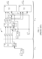
- FIG. 1 shows an example of an SOC 10 with a traditional DFT scheme based on a common clock used to load, propagate and unload test data.
- the SOC 10 includes a first subsystem 12 and a second subsystem 14.
- the first subsystem 12 includes a master register slice 20.
- the second subsystem 14 includes a register slice 22, an asynchronous First In First Out (FIFO) 24 and an asynchronous FIFO 26.
- FIFO First In First Out
- the master register slice 20 transmits to the register slice 22, a data ("Data”) 30a, a write enable for read data (“Wren_r”) 32a, a write enable for address data (Wren_ar”) 34a and a clock 36a, each of which are subsequently retransmitted to both asynchronous FIFOs 24 and 26 as 30b, 32b, 34 and 36b respectively.
- the asynchronous FIFOs 24 and 26 provide outputs 40 and 42 respectively.
- a clock generator 50 generates the clock 36a.
- a multiplexer 52 receives the clock 36a and may selectively generate an output 54, which triggers a clock generator 56 of the register slice 22 to provide the clock 36b.
- a multiplexer 58 receives the clock 36b and may selectively generate an output 60, which clocks each of the asynchronous FIFOs 24 and 26.
- a test clock 62 is gated by Design For Test Clock Gating (DFTCG) circuits 64 and 66.
- a scan mode signal 68 controls the multiplexers 54 and 58 to select either the clocks 36a and 36b respectively, or the gated test clocks of DFTCG 64 and 66 respectively. When the SOC 10 is being tested, the functional clocks 36a and 36b are not selected.
- the gated test clocks from the DFTCG circuits 64 and 66 are used to scan test data into the master slice 20, to propagate the data from the master slice to the register slice 22 and asynchronous FIFOs 24 and 26, and to scan test data out of the SOC 10.
- the gated clocks from the DFTCG circuits 64 and 66 do not test for transition delay (TD) faults that occur when propagation occurs through the register slice 22 without gating.
- TD transition delay
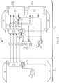
- FIG. 2 shows an SOC 70 including the hierarchical DFT scheme, in accordance with an embodiment of the present disclosure.
- An ExTest signal 72 and a DFT control signal 74 (used to select between a shift and capture phase) are further used to gate the scan mode signal 68.
- the multiplexers 52 and 58 will allow the clock signals 36a and 36b to pass through to the multiplexer outputs 54 and 60 respectively. Otherwise, the multiplexers 52 and 58 will pass the clock signal 62 through to the multiplexer outputs 54 and 60.
- gating the scan mode signal 68 may be conditioned upon one or more signals.
- test clock 62 is used to scan test data into an SSI interface of the master register slice 20.
- the test data is then launched from the master slice 20 along with a functional clock 36a generated by the clock generator 50 and allowed to propagate to the register slice and subsequently to the asynchronous FIFOs 24 and 26.
- test data is thus propagated "at-speed" concurrently with the functional clocks 36a and 36b.
- the test data may be scanned out.
- one or more of the register slice 22 and the asynchronous FIFOs 24 are 26 are referred to as "slaves.”
- the test scheme of FIG. 2 provides true at-speed (e.g., the speed at which the SOC 70 normally operates during normal usage). Furthermore this test scheme is agnostic to the number of intervening register slices between the master register slice 20 and the slaves.
- An SSI interface requires the functional clock 36a to be delayed by approximately 180 degrees relative to the data 30a that it will register (e.g., to provide a good "data eye").
- there may be more than one inversion To ensure that the clock polarity of the functional clock 36a or 36b is the same as the test clock gated by DFTCG 66, each functional clock 36a or 36b may be selectively inverted depending on a corresponding Test Data Register (TDR) bit 76 or 78.
- TDR Test Data Register
- the inversion of the functional clocks 36a, 36b or both 36a and 36b is performed by an "exclusive-OR" logic gate.
- FIG. 3 shows an SOC 80 including the hierarchical DFT scheme, in accordance with another embodiment of the present disclosure.
- the SOC 80 includes a third subsystem 82 interposed between the first subsystem 12 and the second subsystem 14.
- the third subsystem 82 includes an intermediate register 84, which in one example, may be conditionally reset based on the state of a functional reset signal 86 and a scan enable signal 88. In another embodiment, the reset of the intermediate register 84 may be conditioned upon one or more signals. Similar to the register slice 22, the intermediate register 84 retransmits a data signal 30c, a write enable for read data 32c, a write enable for address data 34c and a clock 36c.
- the intermediate register 84 has no scan elements and relies exclusively on the functional clock 36a to propagate the data and functional clock 36a from the first subsystem 12, (which includes the master) to the final subsystem 14, (which includes the slave).
- test data e.g., a "test vector”
- intermediate registers e.g., subsystem 82
- the test data is then captured by the last (e.g., second) subsystem 14 having the slave and scanned out.
- the slave may be one or more of the register slice 22, and the asynchronous FIFOs 24 and 26, each included in the last (e.g., third) subsystem 14.
- the intermediate register 84 is instantiated at a top hierarchical level of the SOC 80 and assists in retiming communications between the subsystems 12 and 14. Testing the intermediate register with the functional clock may improve the fault coverage over the traditional "two clock cycle" test, the later allowing for extra settling time resulting from transistors that may be abnormally slow to transition between states.
- FIG. 4 shows an SOC 90 including scan chain wrappers, in accordance with an embodiment of the present disclosure.
- the SOC 90 includes scan chains 92 and 94 to scan test data into the master register slice 20 from respective scan wrappers 96 and 98.
- the SOC 90 further includes scan chains 100 and 104 to scan test data out of the asynchronous FIFOs 24 and 26 and into respective scan wrappers 106 and 108, and scan chain 102 to scan data between the asynchronous FIFOs 24 and 26.
- the SOC 90 further includes scan chains 110 and 112 to scan test data out of the register slice 22 and into respective scan wrappers 106 and 108.
- each of the scan wrappers 96, 98, 106 and 108 may convert scan data from a higher hierarchical level of the SOC 90 to a serialized format appropriate for interfacing with the master slice 20, register slice 22 and asynchronous FIFOs 24 and 26.
- the higher hierarchical level of the SOC 90 may stitch scan chains together to form one or more concatenated chains.
- Each register slice or FIFO of the SOC 90 forming a master or a slave may have a unique scan chain due to the requirement for configurable clock polarities as described in FIG. 2 .
- “lockups” may be inserted between the scan chains of the register slices and FIFOs to reduce the timing skew between the scan chains forming the concatenated scan chain.
- the term "lockup” as used throughout this disclosure refers to a transparent latch circuit used to resolve a clock skew problem by introducing a half cycle delay in the data path.
- FIG. 5 shows an embodiment 120 of a method for DFT for SSI interfaces.
- a test vector may be shifted into a master register slice 20 of the first subsystem 12 with a DFT clock 62.
- the test vector is shifted into the master register slice 20 from the scan wrappers 96 and 98 through the scan chains 92 and 94 respectively.
- a functional clock 36a is generated with the master register slice 20 (by the clock generator 50).
- the test vector and functional clock 36a is launched from the master register slice 20 from the SSI interface.
- test vector and functional clock 36a are captured with a slave (e.g., one or more of the register slice 22 and the asynchronous FIFOs 24 and 26 of the second subsystem 14.
- a test vector is shifted out of a slave of the second subsystem 14 with the DFT clock 62.
- the test vector may be shifted out of the register slice 22 to the scan wrappers 106 and 108 through the scan chains 110 and 112 respectively.
- the test vector may be shifted out of the asynchronous FIFOs 24 and 26 to the scan wrappers 106 and 108 through the scan chains 100 and 104 respectively.
- the test vector may be shifted out of a combination of the register slice 22 and the asynchronous FIFOs 24 and 26.
- a method for Design For Test (DFT) for Source Synchronous Interfaces (SSI) comprises shifting a test vector into a master register slice with a DFT clock. A functional clock is generated. The test vector and the functional clock are launched from a first SSI of the master register slice. The test vector and the functional clock are captured with a second SSI of a slave. The test vector is shifted out of the slave with the DFT clock.
- DFT Design For Test
- SSI Source Synchronous Interfaces
- Alternative embodiments of the method for Design For Test (DFT) for Source Synchronous Interfaces (SSI) include one of the following features, or any combination thereof.
- a clock input of the slave is selected with a multiplexer, wherein the multiplexer is configured to select one of the functional clock and the DFT clock.
- the DFT clock is selectably inverted to align a first polarity of the functional clock to a second polarity of the DFT clock.
- a first frequency of the functional clock is greater than a second frequency of the DFT clock.
- the test vector and the functional clock are propagated through an intermediate register slice prior to capturing the test vector and the functional clock with the second SSI of the slave, wherein the intermediate register slice is clocked only with the functional clock.
- Shifting the test vector out of the slave comprises shifting a respective data from one or more of a slave register slice and an asynchronous First In First Out (FIFO) register.
- a first scan chain from a slave register slice is concatenated with a second scan chain from an asynchronous First In First Out (FIFO) register, wherein the slave comprises the slave register slice and the asynchronous FIFO register.
- a timing skew between the first scan chain and the second scan chain is resolved with a lockup latch.
- a first subsystem comprises shifting the test vector in with the DFT clock, and a second subsystem comprises shifting a second test vector out with a second DFT clock.
- a functional behavior of the first subsystem is emulated with the test vector.
- an apparatus comprises a master register slice comprising a first Source Synchronous Interface (SSI).
- a slave comprises a second SSI, wherein the second SSI is configured to receive a test vector and a functional clock from the first SSI during a capture mode.
- a multiplexer is connected to the functional clock, a Design For Test (DFT) clock and a clock input of the slave, wherein the multiplexer is configured to select the DFT clock in response to a request to shift out the test vector from the slave and to select the functional clock during the capture mode.
- DFT Design For Test
- a selectable inverter is between the DFT clock and the multiplexer, the selective inverter is configured to invert the DFT clock to align a first polarity of the functional clock to a second polarity of the DFT clock.
- a first frequency of the functional clock is greater than a second frequency of the DFT clock.
- the test vector and the functional clock propagate through an intermediate register slice prior to being captured with the second SSI of the slave, and the intermediate register slice is clocked only with the functional clock.
- the slave comprises one or more of a slave register slice and an asynchronous First In First Out (FIFO) register.
- FIFO First In First Out
- an apparatus comprises a first subsystem comprising a first register comprising a first Source Synchronous Interface (SSI).
- a second subsystem comprises a second register comprising a second SSI, wherein the second SSI is configured to receive a test vector and a functional clock from the first SSI during a capture mode.
- a multiplexer is connected to the functional clock, a Design For Test (DFT) clock and a clock input of the second register, wherein the multiplexer is configured to select the DFT clock in response to a request to shift out the test vector from the second register and to select the functional clock during the capture mode.
- DFT Design For Test
- An intermediate register is interposed between the first register and the second register, wherein the test vector and the functional clock propagate through the intermediate register prior to being captured with the second SSI, and the intermediate register is clocked only with the functional clock.
- the second subsystem further comprises an asynchronous First In First Out (FIFO) register, wherein the second register comprises a first scan chain and the FIFO comprises a second scan chain.
- FIFO First In First Out
- a lockup latch is configured to resolve a timing skew between the first scan chain and the second scan chain.
- the first subsystem comprises a second DFT clock, configured to scan the test vector into the first register.
Landscapes
- Engineering & Computer Science (AREA)
- General Engineering & Computer Science (AREA)
- Physics & Mathematics (AREA)
- General Physics & Mathematics (AREA)
- Computer Hardware Design (AREA)
- Test And Diagnosis Of Digital Computers (AREA)
- Tests Of Electronic Circuits (AREA)
Abstract
A method for Design For Test (DFT) for Source Synchronous Interfaces (SSI) includes shifting a test vector into a master register slice with a DFT clock. A functional clock is generated. The test vector and the functional clock are launched from a first SSI of the master register slice. The test vector and the functional clock are captured with a second SSI of a slave. The test vector is shifted out of the slave with the DFT clock.
Description
- This disclosure relates generally to Design For Test (DFT), and more specifically to a hierarchical DFT scheme for Source Synchronous Interfaces (SSI).
- Large Systems On a Chip (SOC) may contain numerous communication interfaces between the various subsystems. Higher bandwidth is achieved by using SSI between these subsystems. SSI improves bandwidth by transferring a clock and data together, so that the clock and data will be equally delayed, with a limitation that the skew between the clock and data must be less than half of the clock period.
- A traditional "two clock cycle at-speed" test uses a clock edge of one cycle of a local Phase Locked Loop (PLL) to launch data, and the same edge of a subsequent cycle to capture the data, however this test approach is not applicable for SSI interfaces. SSI interfaces have traditionally been tested with a slower DFT clock generator used to scan data into and out of scan chains and also to propagate the data. Accordingly, very low at-speed test coverage has been obtained with this approach.
- The present invention is illustrated by way of example and is not limited by the accompanying figures, in which like references indicate similar elements. Elements in the figures are illustrated for simplicity and clarity and have not necessarily been drawn to scale.
-
FIG. 1 is a schematic view of an example of a System On a Chip (SOC) with a DFT scheme based on a global clock. -
FIG. 2 is a schematic view of an SOC with a hierarchical DFT scheme, in accordance with an embodiment of the present disclosure. -
FIG. 3 is a schematic view of an SOC with a hierarchical DFT scheme, in accordance with another embodiment of the present disclosure. -
FIG. 4 is a schematic view of an SOC with a DFT scheme including scan chain wrappers, in accordance with an embodiment of the present disclosure. -
FIG. 5 is a flowchart representation of a method for DFT for an SOC having an SSI, in accordance with an embodiment of the present disclosure. - Embodiments described herein provide for hierarchical at-speed testing of SOCs having SSI interfaces. A combination of slower DFT clocks are used for serialized transfer of test vectors and higher speed functional clocking is used between registers. Accordingly, high fault coverage is realized, while still maintaining the IEEE 1500 standards support for inter subsystem tests. IEEE 1500 is a standard for embedded core testing supported by the Institute of Electrical and Electronics Engineers (IEEE) association.
-
FIG. 1 shows an example of anSOC 10 with a traditional DFT scheme based on a common clock used to load, propagate and unload test data. The SOC 10 includes afirst subsystem 12 and asecond subsystem 14. Thefirst subsystem 12 includes amaster register slice 20. Thesecond subsystem 14 includes aregister slice 22, an asynchronous First In First Out (FIFO) 24 and anasynchronous FIFO 26. Themaster register slice 20 transmits to theregister slice 22, a data ("Data") 30a, a write enable for read data ("Wren_r") 32a, a write enable for address data (Wren_ar") 34a and aclock 36a, each of which are subsequently retransmitted to bothasynchronous FIFOs asynchronous FIFOs outputs clock generator 50 generates theclock 36a. Amultiplexer 52 receives theclock 36a and may selectively generate anoutput 54, which triggers aclock generator 56 of theregister slice 22 to provide theclock 36b. Amultiplexer 58 receives theclock 36b and may selectively generate anoutput 60, which clocks each of theasynchronous FIFOs test clock 62 is gated by Design For Test Clock Gating (DFTCG)circuits scan mode signal 68, controls themultiplexers clocks DFTCG SOC 10 is being tested, thefunctional clocks DFTCG circuits master slice 20, to propagate the data from the master slice to theregister slice 22 andasynchronous FIFOs SOC 10. The gated clocks from theDFTCG circuits register slice 22 without gating. -
FIG. 2 shows anSOC 70 including the hierarchical DFT scheme, in accordance with an embodiment of the present disclosure. AnExTest signal 72 and a DFT control signal 74 (used to select between a shift and capture phase) are further used to gate thescan mode signal 68. Specifically, when theExTest signal 72 and theDFT control signal 74 are asserted high (e.g., a logical "1" value), themultiplexers multiplexers clock signal 62 through to the multiplexer outputs 54 and 60. In another embodiment, gating thescan mode signal 68 may be conditioned upon one or more signals. During test of theSOC 70, thetest clock 62 is used to scan test data into an SSI interface of themaster register slice 20. The test data is then launched from themaster slice 20 along with afunctional clock 36a generated by theclock generator 50 and allowed to propagate to the register slice and subsequently to theasynchronous FIFOs - The test data is thus propagated "at-speed" concurrently with the
functional clocks register slice 22 and theasynchronous FIFOs register slice 22 and theasynchronous FIFOs 24 are 26 are referred to as "slaves." Accordingly, the test scheme ofFIG. 2 provides true at-speed (e.g., the speed at which theSOC 70 normally operates during normal usage). Furthermore this test scheme is agnostic to the number of intervening register slices between themaster register slice 20 and the slaves. An SSI interface requires thefunctional clock 36a to be delayed by approximately 180 degrees relative to thedata 30a that it will register (e.g., to provide a good "data eye"). Depending upon the number of registers between themaster register slice 20 and the slave, there may be more than one inversion. To ensure that the clock polarity of thefunctional clock DFTCG 66, eachfunctional clock functional clocks -
FIG. 3 with continued reference toFIG. 2 shows anSOC 80 including the hierarchical DFT scheme, in accordance with another embodiment of the present disclosure. TheSOC 80 includes athird subsystem 82 interposed between thefirst subsystem 12 and thesecond subsystem 14. Thethird subsystem 82 includes anintermediate register 84, which in one example, may be conditionally reset based on the state of afunctional reset signal 86 and a scan enablesignal 88. In another embodiment, the reset of theintermediate register 84 may be conditioned upon one or more signals. Similar to theregister slice 22, theintermediate register 84 retransmits adata signal 30c, a write enable forread data 32c, a write enable foraddress data 34c and aclock 36c. - In contrast to the
register slice 22, (e.g. a slave), theintermediate register 84 has no scan elements and relies exclusively on thefunctional clock 36a to propagate the data andfunctional clock 36a from thefirst subsystem 12, (which includes the master) to thefinal subsystem 14, (which includes the slave). Specifically, test data (e.g., a "test vector") is scanned into a register of thefirst subsystem 12, propagated through intermediate registers (e.g., subsystem 82), at-speed and without scan by launching the test vector from an SSI of the master. The test data is then captured by the last (e.g., second)subsystem 14 having the slave and scanned out. In various embodiments, the slave may be one or more of theregister slice 22, and theasynchronous FIFOs subsystem 14. In one embodiment, theintermediate register 84 is instantiated at a top hierarchical level of theSOC 80 and assists in retiming communications between thesubsystems -
FIG. 4 shows anSOC 90 including scan chain wrappers, in accordance with an embodiment of the present disclosure. The SOC 90 includesscan chains master register slice 20 fromrespective scan wrappers SOC 90 further includesscan chains asynchronous FIFOs respective scan wrappers scan chain 102 to scan data between theasynchronous FIFOs SOC 90 further includesscan chains register slice 22 and intorespective scan wrappers - In one embodiment, each of the
scan wrappers SOC 90 to a serialized format appropriate for interfacing with themaster slice 20,register slice 22 andasynchronous FIFOs SOC 90 may stitch scan chains together to form one or more concatenated chains. Each register slice or FIFO of theSOC 90 forming a master or a slave may have a unique scan chain due to the requirement for configurable clock polarities as described inFIG. 2 . When stitching scan chains together, "lockups" may be inserted between the scan chains of the register slices and FIFOs to reduce the timing skew between the scan chains forming the concatenated scan chain. The term "lockup" as used throughout this disclosure refers to a transparent latch circuit used to resolve a clock skew problem by introducing a half cycle delay in the data path. -
FIG. 5 shows anembodiment 120 of a method for DFT for SSI interfaces. With continued reference toFIG. 4 , at 122, a test vector may be shifted into amaster register slice 20 of thefirst subsystem 12 with aDFT clock 62. The test vector is shifted into themaster register slice 20 from thescan wrappers scan chains functional clock 36a is generated with the master register slice 20 (by the clock generator 50). At 126, the test vector andfunctional clock 36a is launched from themaster register slice 20 from the SSI interface. At 128, the test vector andfunctional clock 36a are captured with a slave (e.g., one or more of theregister slice 22 and theasynchronous FIFOs second subsystem 14. At 130, a test vector is shifted out of a slave of thesecond subsystem 14 with theDFT clock 62. - For example, the test vector may be shifted out of the
register slice 22 to thescan wrappers scan chains asynchronous FIFOs scan wrappers scan chains register slice 22 and theasynchronous FIFOs - As will be appreciated, at least some of the embodiments as disclosed include at least the following. In one embodiment, a method for Design For Test (DFT) for Source Synchronous Interfaces (SSI) comprises shifting a test vector into a master register slice with a DFT clock. A functional clock is generated. The test vector and the functional clock are launched from a first SSI of the master register slice. The test vector and the functional clock are captured with a second SSI of a slave. The test vector is shifted out of the slave with the DFT clock.
- Alternative embodiments of the method for Design For Test (DFT) for Source Synchronous Interfaces (SSI) include one of the following features, or any combination thereof. A clock input of the slave is selected with a multiplexer, wherein the multiplexer is configured to select one of the functional clock and the DFT clock. The DFT clock is selectably inverted to align a first polarity of the functional clock to a second polarity of the DFT clock. A first frequency of the functional clock is greater than a second frequency of the DFT clock. The test vector and the functional clock are propagated through an intermediate register slice prior to capturing the test vector and the functional clock with the second SSI of the slave, wherein the intermediate register slice is clocked only with the functional clock. Shifting the test vector out of the slave comprises shifting a respective data from one or more of a slave register slice and an asynchronous First In First Out (FIFO) register. A first scan chain from a slave register slice is concatenated with a second scan chain from an asynchronous First In First Out (FIFO) register, wherein the slave comprises the slave register slice and the asynchronous FIFO register. A timing skew between the first scan chain and the second scan chain is resolved with a lockup latch. A first subsystem comprises shifting the test vector in with the DFT clock, and a second subsystem comprises shifting a second test vector out with a second DFT clock. A functional behavior of the first subsystem is emulated with the test vector.
- In another embodiment, an apparatus comprises a master register slice comprising a first Source Synchronous Interface (SSI). A slave comprises a second SSI, wherein the second SSI is configured to receive a test vector and a functional clock from the first SSI during a capture mode. A multiplexer is connected to the functional clock, a Design For Test (DFT) clock and a clock input of the slave, wherein the multiplexer is configured to select the DFT clock in response to a request to shift out the test vector from the slave and to select the functional clock during the capture mode.
- Alternative embodiments of the apparatus include one of the following features, or any combination thereof. A selectable inverter is between the DFT clock and the multiplexer, the selective inverter is configured to invert the DFT clock to align a first polarity of the functional clock to a second polarity of the DFT clock. A first frequency of the functional clock is greater than a second frequency of the DFT clock. The test vector and the functional clock propagate through an intermediate register slice prior to being captured with the second SSI of the slave, and the intermediate register slice is clocked only with the functional clock. The slave comprises one or more of a slave register slice and an asynchronous First In First Out (FIFO) register.
- In another embodiment, an apparatus comprises a first subsystem comprising a first register comprising a first Source Synchronous Interface (SSI). A second subsystem comprises a second register comprising a second SSI, wherein the second SSI is configured to receive a test vector and a functional clock from the first SSI during a capture mode. A multiplexer is connected to the functional clock, a Design For Test (DFT) clock and a clock input of the second register, wherein the multiplexer is configured to select the DFT clock in response to a request to shift out the test vector from the second register and to select the functional clock during the capture mode.
- Alternative embodiments of the apparatus include one of the following features, or any combination thereof. An intermediate register is interposed between the first register and the second register, wherein the test vector and the functional clock propagate through the intermediate register prior to being captured with the second SSI, and the intermediate register is clocked only with the functional clock. The second subsystem further comprises an asynchronous First In First Out (FIFO) register, wherein the second register comprises a first scan chain and the FIFO comprises a second scan chain. A lockup latch is configured to resolve a timing skew between the first scan chain and the second scan chain. The first subsystem comprises a second DFT clock, configured to scan the test vector into the first register.
- Although the invention is described herein with reference to specific embodiments, various modifications and changes can be made without departing from the scope of the present invention as set forth in the claims below. Accordingly, the specification and figures are to be regarded in an illustrative rather than a restrictive sense, and all such modifications are intended to be included within the scope of the present invention. Any benefits, advantages, or solutions to problems that are described herein with regard to specific embodiments are not intended to be construed as a critical, required, or essential feature or element of any or all the claims.
- Unless stated otherwise, terms such as "first" and "second" are used to arbitrarily distinguish between the elements such terms describe. Thus, these terms are not necessarily intended to indicate temporal or other prioritization of such elements.
Claims (15)
- A method for Design For Test (DFT) for Source Synchronous Interfaces (SSI) comprising:shifting a test vector into a master register slice with a DFT clock;generating a functional clock;launching the test vector and the functional clock from a first SSI of the master register slice;capturing the test vector and the functional clock with a second SSI of a slave; andshifting the test vector out of the slave with the DFT clock.
- The method of claim 1 further comprising selecting a clock input of the slave with a multiplexer, wherein the multiplexer is configured to select one of the functional clock and the DFT clock.
- The method of claim 2 further comprising selectably inverting the DFT clock to align a first polarity of the functional clock to a second polarity of the DFT clock.
- The method of any preceding claim wherein a first frequency of the functional clock is greater than a second frequency of the DFT clock.
- The method of any preceding claim further comprising propagating the test vector and the functional clock through an intermediate register slice prior to capturing the test vector and the functional clock with the second SSI of the slave, wherein the intermediate register slice is clocked only with the functional clock.
- The method of any preceding claim wherein shifting the test vector out of the slave comprises shifting a respective data from one or more of a slave register slice and an asynchronous First In First Out (FIFO) register.
- The method of any preceding claim further comprising concatenating a first scan chain from a slave register slice with a second scan chain from an asynchronous First In First Out (FIFO) register, wherein the slave comprises the slave register slice and the asynchronous FIFO register.
- The method of claim 7 further comprising resolving a timing skew between the first scan chain and the second scan chain with a lockup latch.
- The method of any preceding claim wherein a first subsystem comprises shifting the test vector in with the DFT clock, and a second subsystem comprises shifting a second test vector out with a second DFT clock.
- The method of claim 9 further comprising emulating a functional behavior of the first subsystem with the test vector.
- An apparatus comprising:a master register slice comprising a first Source Synchronous Interface (SSI);a slave comprising a second SSI, wherein the second SSI is configured to receive a test vector and a functional clock from the first SSI during a capture mode; anda multiplexer connected to the functional clock, a Design For Test (DFT) clock and a clock input of the slave, wherein the multiplexer is configured to select the DFT clock in response to a request to shift out the test vector from the slave and to select the functional clock during the capture mode.
- The apparatus of claim 11 further comprising a selectable inverter between the DFT clock and the multiplexer, the selective inverter configured to invert the DFT clock to align a first polarity of the functional clock to a second polarity of the DFT clock.
- The apparatus of claim 11 or 12 wherein a first frequency of the functional clock is greater than a second frequency of the DFT clock.
- The apparatus of any of claims 11 to 13 wherein the test vector and the functional clock propagate through an intermediate register slice prior to being captured with the second SSI of the slave, and the intermediate register slice is clocked only with the functional clock.
- The apparatus of any of claims 11 to 14 wherein the slave comprises one or more of a slave register slice and an asynchronous First In First Out (FIFO) register.
Applications Claiming Priority (1)
| Application Number | Priority Date | Filing Date | Title |
|---|---|---|---|
| IN202221071952 | 2022-12-13 |
Publications (1)
| Publication Number | Publication Date |
|---|---|
| EP4390413A1 true EP4390413A1 (en) | 2024-06-26 |
Family
ID=89164246
Family Applications (1)
| Application Number | Title | Priority Date | Filing Date |
|---|---|---|---|
| EP23215241.3A Pending EP4390413A1 (en) | 2022-12-13 | 2023-12-08 | Design for test for source synchronous interfaces |
Country Status (2)
| Country | Link |
|---|---|
| US (1) | US12553942B2 (en) |
| EP (1) | EP4390413A1 (en) |
Citations (3)
| Publication number | Priority date | Publication date | Assignee | Title |
|---|---|---|---|---|
| EP1873540B1 (en) * | 2006-06-27 | 2009-11-04 | Silicon Image, Inc. | Test clock control structures to generate configurable test clocks for scan-based testing of electronic circuits using programmable test clock controllers |
| US20130218508A1 (en) * | 2012-02-22 | 2013-08-22 | Freescale Semiconductor, Inc | System for testing electronic circuits |
| US20160169971A1 (en) * | 2014-12-15 | 2016-06-16 | Genesys Testware, Inc. | Design-for-Test Techniques for a Digital Electronic Circuit |
Family Cites Families (5)
| Publication number | Priority date | Publication date | Assignee | Title |
|---|---|---|---|---|
| US9234942B2 (en) * | 2012-09-21 | 2016-01-12 | Apple Inc. | Transition fault testing of source synchronous interface |
| US10444280B2 (en) * | 2015-10-27 | 2019-10-15 | Nvidia Corporation | Independent test partition clock coordination across multiple test partitions |
| US20170149555A1 (en) | 2015-11-20 | 2017-05-25 | Qualcomm Incorporated | Self-test for source-synchronous interface |
| US11257560B2 (en) * | 2017-09-27 | 2022-02-22 | Intel Corporation | Test architecture for die to die interconnect for three dimensional integrated circuits |
| US11934219B2 (en) * | 2022-03-29 | 2024-03-19 | Qualcomm Incorporated | Integrated functional and design for testability (DFT) clock delivery architecture |
-
2023
- 2023-02-14 US US18/168,643 patent/US12553942B2/en active Active
- 2023-12-08 EP EP23215241.3A patent/EP4390413A1/en active Pending
Patent Citations (3)
| Publication number | Priority date | Publication date | Assignee | Title |
|---|---|---|---|---|
| EP1873540B1 (en) * | 2006-06-27 | 2009-11-04 | Silicon Image, Inc. | Test clock control structures to generate configurable test clocks for scan-based testing of electronic circuits using programmable test clock controllers |
| US20130218508A1 (en) * | 2012-02-22 | 2013-08-22 | Freescale Semiconductor, Inc | System for testing electronic circuits |
| US20160169971A1 (en) * | 2014-12-15 | 2016-06-16 | Genesys Testware, Inc. | Design-for-Test Techniques for a Digital Electronic Circuit |
Also Published As
| Publication number | Publication date |
|---|---|
| US12553942B2 (en) | 2026-02-17 |
| US20240192271A1 (en) | 2024-06-13 |
Similar Documents
| Publication | Publication Date | Title |
|---|---|---|
| US8717078B2 (en) | Sequential latching device with elements to increase hold times on the diagnostic data path | |
| US7843218B1 (en) | Data latch with structural hold | |
| US6968486B2 (en) | Master-slave-type scanning flip-flop circuit for high-speed operation with reduced load capacity of clock controller | |
| US8484523B2 (en) | Sequential digital circuitry with test scan | |
| US7543207B2 (en) | Full scan solution for latched-based design | |
| USRE41496E1 (en) | Boundary-scan input circuit for a reset pin | |
| US9612281B2 (en) | High-speed flip-flop with robust scan-in path hold time | |
| US5721740A (en) | Flip-flop controller for selectively disabling clock signal | |
| US5293079A (en) | Formatter circuit | |
| US8841952B1 (en) | Data retention flip-flop | |
| US8644439B2 (en) | Circuits and methods for signal transfer between different clock domains | |
| US5313470A (en) | Boundary-scan input cell for a clock pin | |
| US8375265B1 (en) | Delay fault testing using distributed clock dividers | |
| EP1890234B1 (en) | Microcomputer and method for testing the same | |
| US20140298126A1 (en) | Latch circuit, scan test circuit and latch circuit control method | |
| US12203984B2 (en) | Scan chain circuit and corresponding method | |
| EP0927386A1 (en) | Transmitter and receiver circuits for high-speed parallel digital data transmission link | |
| US12553942B2 (en) | Test for source synchronous interfaces | |
| JP3363691B2 (en) | Semiconductor logic integrated circuit | |
| US20060085707A1 (en) | High speed energy conserving scan architecture | |
| US20130166978A1 (en) | Integrated circuit | |
| US6748563B1 (en) | Method and apparatus for testing path delays in a high-speed boundary scan implementation | |
| US7962805B1 (en) | System and method for preventing a race condition | |
| JP2918730B2 (en) | Scan circuit for digital logic | |
| KR102923642B1 (en) | Semiconductor device including scan chain having scan cells, method thereof, and method of operating semiconductor system capable of locating faulty scan cell among the scan cells |
Legal Events
| Date | Code | Title | Description |
|---|---|---|---|
| PUAI | Public reference made under article 153(3) epc to a published international application that has entered the european phase |
Free format text: ORIGINAL CODE: 0009012 |
|
| STAA | Information on the status of an ep patent application or granted ep patent |
Free format text: STATUS: THE APPLICATION HAS BEEN PUBLISHED |
|
| AK | Designated contracting states |
Kind code of ref document: A1 Designated state(s): AL AT BE BG CH CY CZ DE DK EE ES FI FR GB GR HR HU IE IS IT LI LT LU LV MC ME MK MT NL NO PL PT RO RS SE SI SK SM TR |
|
| STAA | Information on the status of an ep patent application or granted ep patent |
Free format text: STATUS: REQUEST FOR EXAMINATION WAS MADE |
|
| 17P | Request for examination filed |
Effective date: 20250102 |