EP4390367A1 - Measuring device and method for producing measuring device - Google Patents
Measuring device and method for producing measuring device Download PDFInfo
- Publication number
- EP4390367A1 EP4390367A1 EP22307000.4A EP22307000A EP4390367A1 EP 4390367 A1 EP4390367 A1 EP 4390367A1 EP 22307000 A EP22307000 A EP 22307000A EP 4390367 A1 EP4390367 A1 EP 4390367A1
- Authority
- EP
- European Patent Office
- Prior art keywords
- semiconductor layer
- flow channel
- measuring device
- cavity
- sensing module
- Prior art date
- Legal status (The legal status is an assumption and is not a legal conclusion. Google has not performed a legal analysis and makes no representation as to the accuracy of the status listed.)
- Pending
Links
Images






Classifications
-
- G—PHYSICS
- G01—MEASURING; TESTING
- G01N—INVESTIGATING OR ANALYSING MATERIALS BY DETERMINING THEIR CHEMICAL OR PHYSICAL PROPERTIES
- G01N15/00—Investigating characteristics of particles; Investigating permeability, pore-volume or surface-area of porous materials
- G01N15/10—Investigating individual particles
-
- B—PERFORMING OPERATIONS; TRANSPORTING
- B01—PHYSICAL OR CHEMICAL PROCESSES OR APPARATUS IN GENERAL
- B01L—CHEMICAL OR PHYSICAL LABORATORY APPARATUS FOR GENERAL USE
- B01L3/00—Containers or dishes for laboratory use, e.g. laboratory glassware; Droppers
- B01L3/50—Containers for the purpose of retaining a material to be analysed, e.g. test tubes
- B01L3/502—Containers for the purpose of retaining a material to be analysed, e.g. test tubes with fluid transport, e.g. in multi-compartment structures
- B01L3/5027—Containers for the purpose of retaining a material to be analysed, e.g. test tubes with fluid transport, e.g. in multi-compartment structures by integrated microfluidic structures, i.e. dimensions of channels and chambers are such that surface tension forces are important, e.g. lab-on-a-chip
- B01L3/502707—Containers for the purpose of retaining a material to be analysed, e.g. test tubes with fluid transport, e.g. in multi-compartment structures by integrated microfluidic structures, i.e. dimensions of channels and chambers are such that surface tension forces are important, e.g. lab-on-a-chip characterised by the manufacture of the container or its components
-
- B—PERFORMING OPERATIONS; TRANSPORTING
- B01—PHYSICAL OR CHEMICAL PROCESSES OR APPARATUS IN GENERAL
- B01L—CHEMICAL OR PHYSICAL LABORATORY APPARATUS FOR GENERAL USE
- B01L3/00—Containers or dishes for laboratory use, e.g. laboratory glassware; Droppers
- B01L3/50—Containers for the purpose of retaining a material to be analysed, e.g. test tubes
- B01L3/502—Containers for the purpose of retaining a material to be analysed, e.g. test tubes with fluid transport, e.g. in multi-compartment structures
- B01L3/5027—Containers for the purpose of retaining a material to be analysed, e.g. test tubes with fluid transport, e.g. in multi-compartment structures by integrated microfluidic structures, i.e. dimensions of channels and chambers are such that surface tension forces are important, e.g. lab-on-a-chip
- B01L3/502715—Containers for the purpose of retaining a material to be analysed, e.g. test tubes with fluid transport, e.g. in multi-compartment structures by integrated microfluidic structures, i.e. dimensions of channels and chambers are such that surface tension forces are important, e.g. lab-on-a-chip characterised by interfacing components, e.g. fluidic, electrical, optical or mechanical interfaces
-
- B—PERFORMING OPERATIONS; TRANSPORTING
- B01—PHYSICAL OR CHEMICAL PROCESSES OR APPARATUS IN GENERAL
- B01L—CHEMICAL OR PHYSICAL LABORATORY APPARATUS FOR GENERAL USE
- B01L3/00—Containers or dishes for laboratory use, e.g. laboratory glassware; Droppers
- B01L3/50—Containers for the purpose of retaining a material to be analysed, e.g. test tubes
- B01L3/502—Containers for the purpose of retaining a material to be analysed, e.g. test tubes with fluid transport, e.g. in multi-compartment structures
- B01L3/5027—Containers for the purpose of retaining a material to be analysed, e.g. test tubes with fluid transport, e.g. in multi-compartment structures by integrated microfluidic structures, i.e. dimensions of channels and chambers are such that surface tension forces are important, e.g. lab-on-a-chip
- B01L3/502761—Containers for the purpose of retaining a material to be analysed, e.g. test tubes with fluid transport, e.g. in multi-compartment structures by integrated microfluidic structures, i.e. dimensions of channels and chambers are such that surface tension forces are important, e.g. lab-on-a-chip specially adapted for handling suspended solids or molecules independently from the bulk fluid flow, e.g. for trapping or sorting beads or physically stretching molecules
-
- B—PERFORMING OPERATIONS; TRANSPORTING
- B01—PHYSICAL OR CHEMICAL PROCESSES OR APPARATUS IN GENERAL
- B01L—CHEMICAL OR PHYSICAL LABORATORY APPARATUS FOR GENERAL USE
- B01L2200/00—Solutions for specific problems relating to chemical or physical laboratory apparatus
- B01L2200/06—Fluid handling related problems
- B01L2200/0647—Handling flowable solids, e.g. microscopic beads, cells, particles
- B01L2200/0652—Sorting or classification of particles or molecules
-
- B—PERFORMING OPERATIONS; TRANSPORTING
- B01—PHYSICAL OR CHEMICAL PROCESSES OR APPARATUS IN GENERAL
- B01L—CHEMICAL OR PHYSICAL LABORATORY APPARATUS FOR GENERAL USE
- B01L2300/00—Additional constructional details
- B01L2300/06—Auxiliary integrated devices, integrated components
- B01L2300/0627—Sensor or part of a sensor is integrated
-
- B—PERFORMING OPERATIONS; TRANSPORTING
- B01—PHYSICAL OR CHEMICAL PROCESSES OR APPARATUS IN GENERAL
- B01L—CHEMICAL OR PHYSICAL LABORATORY APPARATUS FOR GENERAL USE
- B01L2300/00—Additional constructional details
- B01L2300/06—Auxiliary integrated devices, integrated components
- B01L2300/0627—Sensor or part of a sensor is integrated
- B01L2300/0645—Electrodes
-
- B—PERFORMING OPERATIONS; TRANSPORTING
- B01—PHYSICAL OR CHEMICAL PROCESSES OR APPARATUS IN GENERAL
- B01L—CHEMICAL OR PHYSICAL LABORATORY APPARATUS FOR GENERAL USE
- B01L2300/00—Additional constructional details
- B01L2300/08—Geometry, shape and general structure
- B01L2300/0809—Geometry, shape and general structure rectangular shaped
- B01L2300/0816—Cards, e.g. flat sample carriers usually with flow in two horizontal directions
-
- G—PHYSICS
- G01—MEASURING; TESTING
- G01N—INVESTIGATING OR ANALYSING MATERIALS BY DETERMINING THEIR CHEMICAL OR PHYSICAL PROPERTIES
- G01N15/00—Investigating characteristics of particles; Investigating permeability, pore-volume or surface-area of porous materials
- G01N15/10—Investigating individual particles
- G01N15/1023—Microstructural devices for non-optical measurement
-
- G—PHYSICS
- G01—MEASURING; TESTING
- G01N—INVESTIGATING OR ANALYSING MATERIALS BY DETERMINING THEIR CHEMICAL OR PHYSICAL PROPERTIES
- G01N15/00—Investigating characteristics of particles; Investigating permeability, pore-volume or surface-area of porous materials
- G01N15/10—Investigating individual particles
- G01N15/1031—Investigating individual particles by measuring electrical or magnetic effects
-
- G—PHYSICS
- G01—MEASURING; TESTING
- G01N—INVESTIGATING OR ANALYSING MATERIALS BY DETERMINING THEIR CHEMICAL OR PHYSICAL PROPERTIES
- G01N15/00—Investigating characteristics of particles; Investigating permeability, pore-volume or surface-area of porous materials
- G01N15/10—Investigating individual particles
- G01N2015/1024—Counting particles by non-optical means
Definitions
- the present disclosure relates to a measuring device for measuring a physical characteristic of an object in fluid flow and a method for producing a measuring device having the corresponding configuration.
- Biophysical cytometers based on MEMS (Microelectromechanical systems) technology are useful to perform high content analysis of biological objects such as individual cells and subsequent sorting of the objects according to their biophysical characteristics. Those cytometers may be used, for example, to identify cancer cells for the diagnostic purpose.
- WO 2021/069446 discloses such examples of flow cytometers comprising MEMS actuators and sensors. MEMS technology enables integration of a sensing module with a micro flow channel with detailed designs in the order of hundreds of nanometers to tens of micrometers.
- measuring systems for providing biophysical analysis of cells are available from:
- each electrode must be in electrical isolation to improve the quality of sensed signals.
- the effect of nearby structures and electrical parasitics need to be minimized in order to provide reliable measurement and broader bandwidth.
- the present disclosure aims to improve the signal quality obtained by a measuring device in order to allow physical analysis of target objects in fluid flow.
- a method for producing a measuring device for measuring physical characteristics of objects such as individual cells in fluid flow comprising a microfluidic chip provided with a flow channel for allowing fluid flow and an electrical sensing module including at least two electrodes and configured to acquire a physical characteristic of an object in the fluid flow; the method comprising: preparing an SOI substrate comprising a first semiconductor layer, a second semiconductor layer and an oxide layer provided between the first semiconductor layer and the second semiconductor layer, patterning at least the first semiconductor layer to form a cavity, the cavity defining lateral walls of the flow channel, a bottom wall of the flow channel connecting the lateral walls and the at least two electrodes, the cavity further defining a gap adjacent to each electrode along the flow channel; and applying an insulating material to each gap to form an insulating filling for electrically insulating the electrical sensing module from the remaining first semiconductor layer.
- the insulating material may be a non-photo-patternable material, the applying of the insulating material further comprising: applying the insulating material to the cavity; applying a mask layer onto the insulating material in the cavity; patterning the mask layer according to a contour of each gap; and removing the insulating material according to the patterned mask layer.
- the insulating material may be a photo-patternable material, the applying of the insulating material further comprising: applying the insulating material to the cavity; and removing the insulating material in the cavity according to a contour of each gap.
- the insulating material may be applied to each gap such that the insulating filling is substantially flush with the remaining first semiconductor layer.
- the cavity may be formed to expose the oxide layer.
- the cavity may be formed to expose the second semiconductor layer.
- the method may further comprise: patterning at least the second semiconductor layer to form a further cavity in the second semiconductor layer to expose a portion of the oxide layer opposite which the electrical sensing module is provided, or to expose the first semiconductor layer; and applying an insulating material to the cavity to form an insulating filling for electrically insulating the electrical sensing module from the remaining second semiconductor layer.
- a measuring device for measuring physical characteristics of objects such as individual cells in fluid flow
- the measuring device comprising: a microfluidic chip including a flow channel configured to allow for fluid flow and an electrical sensing module configured to acquire a physical characteristic of an object in the fluid flow
- the chip comprises: a first semiconductor layer; a second semiconductor layer; and an oxide layer provided between the first and second semiconductor layers, wherein the first semiconductor layer is provided with a cavity, the cavity defining lateral walls of the flow channel and a bottom wall of the flow channel connecting the lateral walls
- the electrical sensing module comprises: at least two electrodes, one of the at least two electrodes being provided on one of the lateral walls of the flow channel, another of the at least two electrodes being provided on the other of the lateral walls of the flow channel
- the measuring device further comprises an insulating filing provided adjacent to each electrode along the flow channel and configured to electrically isolate each electrode from the first semiconductor layer.
- the electrical sensing module may comprise at least four electrodes, the insulating fillings being configured to electrically isolate the electrodes from each other.
- an interface between each electrode and the adjacent insulating material may be airtight.
- the second semiconductor layer may be provided with a further cavity filled with an insulating filling that is in contact with the oxide layer opposite the first semiconductor layer or in direct contact with the first semiconductor layer.
- the measuring device may further comprise a mechanical sensing module spaced apart from the electrical sensing module along the flow channel and configured to acquire a mechanical characteristic of the object in the fluid flow.
- the mechanical sensing module may comprise a manipulator provided on one of the lateral walls of the flow channel and a sensor provided on the other of the lateral walls of the flow channel.
- the measuring device 10 may be used for a flow cytometer in order to perform biophysical characterization of objects such as individual cells flowing in a predefined channel, as described below by way of example.
- the flow cytometer may be used to identify cancer cells from the samples introduced into the channel with fluid flow.
- the general concept of the flow cytometer is well known in the art and thus detailed explanations are omitted in the present disclosure. Nonetheless, the possible application of the measuring device 10 disclosed herein is not limited to characterization of individual cells.
- the measuring device 10 may also be used for characterization of other objects, including, but not being limited to, microbeads (e.g. polymer and silica), gels (e.g. DNA gels and cell culturing gels), organoids, liposomes, and exosomes.
- the measuring device 10 comprises a microfluidic chip 20 provided with a flow channel 22 configured to allow for fluid flow that carries cells (a single cell X is schematically shown in figure 1 ) subjected to biophysical characterization.
- Cells are provided in the form of cell suspension or in any other forms compatible with the flow cytometry.
- the chip 20 has a silicon-based layered structure made from an SOI (Silicon on Insulator) wafer, comprising a top silicon layer 21, a bottom silicon layer 25, and a silicon oxide layer 23 between the silicon layers 21 and 25.
- the flow channel 22 is in the form of a cavity formed in the top silicon layer 21.
- the flow channel 22 is delimited by a pair of opposing lateral walls 22a and 22b and a bottom wall 22c connecting the lateral walls 22a and 22b.
- a cover layer such as a PDMS (polydimethylsiloxane) layer is fitted on the top silicon layer 21, thereby the flow channel 22 has a substantially closed structure over an area where the biophysical characterization takes place, while allowing for required installation of the measuring device 10 and connections of electrical components.
- the cover layer may also be formed from other polymers, or another material not limited to but including glass, quartz, or other wafers with a dielectric coating.
- the cover layer is provided with an inlet of the flow channel 22 where the cells are introduced and an outlet of the flow channel 22 connected to a vacuum pump (not shown) for creating continuous fluid flow within the flow channel 22.
- the chip 20 also includes an electric sensing module 30 for acquiring physical properties of the cells in the flow channel 22.
- the physical characteristics to be acquired by the electric sensing module 30 are not limited to, but may include, cell size, membrane capacitance and cytoplasm resistivity.
- the electrical sensing module 30 includes at least one driving electrode 32 and at least one sensing electrode 34.
- the driving electrode 32 provided on the lateral wall 22a of the flow channel 22.
- the sensing electrode 34 provided on the lateral wall 22b opposite the lateral wall 22a where the driving electrode 32 is provided.
- the distance between the electrodes 32 and 34 may be tens of micrometers.
- the electrodes 32 and 34 have a height equivalent to the thickness of the top silicon layer 21.
- the flow channel 22 may have a relatively small width in the area where the electrical sensing module 30 is provided in such a way that a single object, e.g. a cell, passes through at a time for the electrical characterization.
- the electrical sensing module 30 may include two or more of the driving electrodes 32 and two or more of the sensing electrodes 34, each driving electrodes 32 being operated in different driving modes.
- the electrical sensing module 30 may include one driving electrode 32 on the lateral wall 22a and two or more sensing electrodes 34 provided on another lateral wall 22b.
- insulators 36 Adjacent to the driving electrodes 32 and the sensing electrodes 34, insulators 36 are provided.
- the insulators 36 adjacent to the driving electrodes 32 electrically isolate the driving electrodes 32 from each other and from the remaining top silicon layer 21 of the chip 20.
- the insulators 36 adjacent to the sensing electrodes 34 electrically isolate the sensing electrodes 34 from each other and from the remaining silicon layer 21.
- the interface between the insulator 36 and the driving electrodes 32 as well as the interface between the insulator 36 and the sensing electrode 34 is airtight to prevent fluid leakage from the flow channel 22.
- the insulators 36 may be made of any suitable material for the purpose of providing electrical insulation, including but not being limited to CYTOP (TM) or SU8.
- the chip may also comprise a mechanical sensing module 40 for performing mechanical characterization of the cells.
- the mechanical sensing module 40 is integrated with the chip 20.
- the mechanical sensing module 40 includes a manipulator 42 and a mechanical sensor 44.
- the manipulator 42 may be a stationary component in the form of a narrower passage as shown in figure 1 .
- the mechanical sensor 44 may be a displacement sensor configured to detect displacement based on changes in capacitance in response to the individual cells flowing through the mechanical sensing module 40.
- the flow channel 22 is sufficiently narrow in an area where the mechanical sensing module 40 is provided, whereby a cell reaching the narrow passage is subjected to deformation.
- the mechanical sensor 44 detects the reaction of the cells, thereby acquiring mechanical properties of the cell, including but not limited to rigidity or viscosity.
- the manipulator may also be an adjustable manipulator configured to move toward or away from the opposing mechanical sensor 44, compressing a cell flowing the passage between the mobile manipulator and the mechanical sensor 44 in a controlled manner.
- the chip 20 may have an insulating filling 27 (see figure 2 ) in a cavity formed in the bottom silicon layer 25 over an area where the electrical sensing module 30 is disposed, or in other words the area where the measurement takes place by the electrical sensing module 30.
- the cell suspension is introduced from the inlet of the flow channel 22, passing through the electrical sensing module 30 and the mechanical sensing module 40 where the respective biophysical characterizations take place.
- a voltage is applied between the driving electrode 32 and the sensing electrode 34 at different frequencies, thereby generating an electric current flowing through the flow channel 22 and between the electrodes 32 and 34.
- the resistivity of the flow channel 22 locally increases. By measuring the increased resistivity, the electrical signatures of the individual cells are acquired. The presence of the cell also affects the vertical distribution of the electrical field in the channel.
- the insulators 36 separate the driving electrodes 32 from each other and from the top silicon layer 21. Therefore, a parasitic current that could possibly have been generated between them can be prevented and thus the signal quality sensed by the sensing electrode 34 is improved.
- the interfaces between the electrodes 32 and 34 and the insulators 36 are airtight.
- no slit is formed, unlike some existing devices, between the driving electrode 32 and the adjacent channel wall of the top silicon layer 21 as well as between the sensing electrode 34 and the adjacent channel wall. This ensures that introduction of the fluid into the flow channel 22 is performed efficiently because no air enters the flow channel 22 through those slits during the process of applying negative pressure at the outlet of the channel.
- such slits would have affected the signal quality sensed by the sensing module 34 due to parasitic signals that is to be generated between the electrodes and channel walls before and after passage of the flowing cells, in particular in case of fluid flow having a high flow rate. Therefore, the airtight structure of the present disclosure also contributes to the signal quality.
- the optional formation of the insulating filling 27 in the bottom silicon layer 25 is also advantageous to further improve the signal quality. Without the insulating filling 27 behind the oxide layer 23, the bottom silicon layer 25 would have acted as an additional electrode that captures part of the electric current otherwise flowing between the electrodes 32 and 34 across the flow channel 22. This would have affected electrical signals sensed by the sensing electrode 34, depending on the distance between the flowing cell and the bottom silicon layer 25. The presence of the insulating filling 27 prevents the dispersion in measurement result, thereby enabling trajectory-free measurement.
- the insulating filling 27 also prevents electric coupling between the top silicon layer 21 and the bottom silicon layer 25 which would have occurred in particular when the electrical sensing module 30 is operated at a high frequency of about 10 MHz or higher. Due to the presence of the insulating filing 27 underneath the electrical sensing module 30, the measurement device 10 is operable at high frequencies without affecting in measurement result.
- the optional mechanical sensing module 40 enables integration of the system for performing the mechanical characterization of the individual cells in addition to the electrical characterization.
- the measuring device 10 thus provides single-cell impedance spectroscopy in a continuous, uninterrupted flow, thereby achieving high throughput with improved measurement accuracy.
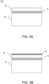
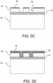
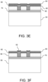
- FIGS 3A to 3H show the process of making a measuring device 10 according to one embodiment.
- the measuring device 10 in particular the chip 20 is made from an SOI (Silicon on Insulator) substrate 100.
- SOI Silicon on Insulator
- MEMS Micro Electro Mechanical Systems
- the SOI substrate 100 comprises a bottom semiconductor layer 50, an oxide layer 70 provided on the bottom semiconductor layer 50, and a top semiconductor layer 90 provided on the oxide layer 70 ( figure 3A ).
- Aluminum coating is then applied onto the top semiconductor layer 90, forming a protective layer 60 ( figure 3B ).
- the protective layer 60 is patterned by means of photolithography and the top semiconductor layer 90 is patterned by means of DRIE etching (Deep Reactive Ion Etching) to form a cavity corresponding to the shapes of the flow channel 20, the electrical sensing module 30 and gaps 92 adjacent to the electrical sensing module 30 ( figure 3C ).
- the mechanical sensing module 40 is also provided in the process.
- An insulating material 80 such as CYTOP (TM) is applied to the gap 92 as well as onto the top of the protective layer 60, for example, by means of deposition ( figure 3D ).
- the protective layer 62 is patterned by photolithography and removed by etching, leaving a portion where the gaps 92 are formed (See figure 3F together with figure 3C ).
- a portion of the insulating material 80 which is not covered by the patterned protective layer 62 is removed, for example, by plasma etching ( figure 3G ).
- the remaining protective layer 62 is then removed and the insulating material 80 underneath the protective layer 62 is removed by plasma etching to form the insulating filling 81 having a surface substantially in flush with the top of the top semiconductor layer 90 ( figure 3H ).
- Keeping the insulating filling 80 flush with the top semiconductor layer 90 is advantageous since it improves adherence of the cover layer such as a PDMS cover film over the entirety of the measuring device 10, in particular the sensing area, thereby preventing fluid leakage from the sensing area.
- the measuring device comprising the individually polarizable electrodes and the preferred electrical isolations are produced.
- the method is advantageously compatible with mass production of the measuring device 10 integrated with the electrical sensing module 30 and optionally with the mechanical sensing module 40.
- a photoresist such as SU8 is applied by deposition in the gaps 92 and on the top of the protective layer 60 ( figure 4D ), to obtain a photoresist layer 82.
- the photoresist layer 82 is patterned by photolithography to remove the portion covering the top of the protective layer 60 to form an insulating filling 81 within the gaps 92 ( figure 4E ).
- the oxide layer 70 may also be removed in order to expose the bottom semiconductor layer 50 behind the oxide layer 70.
- the protective coating 110 is patterned by photolithography to expose a portion of the bottom semiconductor layer 50 where the insulating filling is to be provided ( figure 5B ).
- a portion of the first semiconductor layer 50 which was not covered by the protective layer 110 is removed by DRIE to form cavities 112 ( figure 5C ).
- An insulating material for example, PDMS, is locally deposited to the cavities 112 ( figure 5D ) to obtain an insulating filling 120 in the cavities 112 ( figure 5D ).
- the protective layer 110 is removed to expose the bottom of the remaining first semiconductor layer 50 ( figure 5E ).
- the removal of the protective layer 110 is optional.
- the protective layer 110 may remain in the measuring device 10, provided that the protective layer 110 is grounded.
- the method described above with reference to figures 5A to 5E is also advantageously compatible with mass production of the measuring device 10 having the insulator on the side of the device opposite the electrical sensing module 30.
- the method may further involve removal of a portion of the oxide layer 70 during the process of forming the cavities 112 in order to expose the top semiconductor layer 90 behind the oxide layer 70.
Landscapes
- Chemical & Material Sciences (AREA)
- Health & Medical Sciences (AREA)
- Analytical Chemistry (AREA)
- General Health & Medical Sciences (AREA)
- Dispersion Chemistry (AREA)
- Clinical Laboratory Science (AREA)
- Hematology (AREA)
- Chemical Kinetics & Catalysis (AREA)
- Physics & Mathematics (AREA)
- Fluid Mechanics (AREA)
- Life Sciences & Earth Sciences (AREA)
- Biochemistry (AREA)
- General Physics & Mathematics (AREA)
- Immunology (AREA)
- Pathology (AREA)
- Investigating Or Analyzing Materials By The Use Of Electric Means (AREA)
Abstract
Description
- The present disclosure relates to a measuring device for measuring a physical characteristic of an object in fluid flow and a method for producing a measuring device having the corresponding configuration.
- Biophysical cytometers based on MEMS (Microelectromechanical systems) technology are useful to perform high content analysis of biological objects such as individual cells and subsequent sorting of the objects according to their biophysical characteristics. Those cytometers may be used, for example, to identify cancer cells for the diagnostic purpose.
WO 2021/069446 discloses such examples of flow cytometers comprising MEMS actuators and sensors. MEMS technology enables integration of a sensing module with a micro flow channel with detailed designs in the order of hundreds of nanometers to tens of micrometers. - Other examples of measuring systems for providing biophysical analysis of cells are available from:
- (1) C. Honrado, P. Bisegna, N. S. Swami and F. Caselli, Single-cell microfluidic impedance cytometry: from raw signals to cell phenotypes using data analyticsLab Chip, 21, pp.22-54, (2021);
- (2) Petchakup, C.; Li, K.H.H.; Hou, H.W., Advances in Single Cell Impedance Cytometry for Biomedical Applications, Micromachines 2017, 8, 87;
- (3) Gawad S, Sun T, Green NG, Morgan H, Impedance spectroscopy using maximum length sequences: Application to single cell analysis (2007) Rev Sci Instrum 78:054301; and
- (4) Q. Rezard, G. Perret, J.C. Gerbedoen, et al., IEEE Int. Conf. on MEMS (MEMS'21), pp. 494, (2021). Those microfluidic devices may be made from an SOI (Silicon on Insulator) wafer since it is compatible with integration of MEMS components. Some examples using SOI wafers are available from:
- (5) S. Sharma, K. Buchholz, S. M. Luber, U. Rant, M. Tornow, and G. Abstreiter, "Silicon-on-Insulator Microfluidic Device With Monolithic Sensor Integration for MicroTAS Applications," Journal of Microelectromechanical Systems, vol. 15, no. 2, pp. 308-313, 2006, doi: 10.1109/jmems.2006.872222;
- (6) T. Chingfu and H. Chenghan, "Thermal Bubble Microfluidic Gate Based on SOI Wafer," Journal of Microelectromechanical Systems, vol. 18, no. 4, pp. 852-859, 2009, doi: 10.1109/jmems.2009.2023882;
- (7) B. Legrand, A. E. Ashcroft, L. Buchaillot, and S. Arscott, "SOI-based nanoelectrospray emitter tips for mass spectrometry: a coupled MEMS and microfluidic design," J. Micromech. Microeng., vol. 17, no. 3, pp. 509-514, 2007/02/06 2007, doi: 10.1088/0960-1317/17/3/013;
- (8) https://www.xfab.com/technology/silicon-based-microfluidics;
- (9) C. Adamopoulos, A. Gharia, A. Niknejad, V. Stojanovic, and M. Anwar, "Microfluidic Packaging Integration with Electronic-Photonic Biosensors Using 3D Printed Transfer Molding," Biosensors (Basel), vol. 10, no. 11, Nov 14 2020, doi: 10.3390/bios10110177;
- (10) https://www.micralyne.com/technology-platforms/micrafluidics-silicon-microfluidic-mems-process/
- (11) R. Reale, A. De Ninno, L. Businaro, P. Bisegna, and F. Caselli, "High-throughput electrical position detection of single flowing particles/cells with non-spherical shape," Lab Chip, 10.1039/C9LC00071B vol. 19, no. 10, pp. 1818-1827, May 14 2019, doi: 10.1039/c9lc00071b;
- (12) S. Gawad, L. Schild, and P. Renaud, "Micromachined impedance spectroscopy flow cytometer for cell analysis and particle sizing," Lab on a Chip, vol. 1, no. 1, pp. 76-82, 2001, doi: 10.1039/b103933b;
- (13) E. Rollo et al., "Label-free identification of activated T lymphocytes through tridimensional microsensors on chip," Biosensors and Bioelectronics, vol. 94, pp. 193-199, Aug 15 2017, doi: 10.1016/j.bios.2017.02.047;
- (14) X. Huang et al., "Self-aligned sequential lateral field non-uniformities over channel depth for high throughput dielectrophoretic cell deflection," Lab Chip, vol. 21, no. 5, pp. 835-843, Mar 9 2021, doi: 10.1039/d0lc01211d; and
- (15) S. M. Weiz, M. Medina-Sánchez, and O. G. Schmidt, "Microsystems for Single-Cell Analysis," Advanced Biosystems, vol. 2, no. 2, 2018, doi: 10.1002/adbi.201700193.
- There is, however, some limitation in the proposed systems. For example, a silicon wafer requires each electrode to be in electrical isolation to improve the quality of sensed signals. Also, the effect of nearby structures and electrical parasitics need to be minimized in order to provide reliable measurement and broader bandwidth.
- The present disclosure aims to improve the signal quality obtained by a measuring device in order to allow physical analysis of target objects in fluid flow.
- According to the present invention, there is provided a method for producing a measuring device for measuring physical characteristics of objects such as individual cells in fluid flow, the measuring device comprising a microfluidic chip provided with a flow channel for allowing fluid flow and an electrical sensing module including at least two electrodes and configured to acquire a physical characteristic of an object in the fluid flow; the method comprising: preparing an SOI substrate comprising a first semiconductor layer, a second semiconductor layer and an oxide layer provided between the first semiconductor layer and the second semiconductor layer, patterning at least the first semiconductor layer to form a cavity, the cavity defining lateral walls of the flow channel, a bottom wall of the flow channel connecting the lateral walls and the at least two electrodes, the cavity further defining a gap adjacent to each electrode along the flow channel; and applying an insulating material to each gap to form an insulating filling for electrically insulating the electrical sensing module from the remaining first semiconductor layer.
- According to one aspect of the present invention, the insulating material may be a non-photo-patternable material, the applying of the insulating material further comprising: applying the insulating material to the cavity; applying a mask layer onto the insulating material in the cavity; patterning the mask layer according to a contour of each gap; and removing the insulating material according to the patterned mask layer.
- According to one aspect of the present invention, the insulating material may be a photo-patternable material, the applying of the insulating material further comprising: applying the insulating material to the cavity; and removing the insulating material in the cavity according to a contour of each gap.
- According to one aspect of the present invention, the insulating material may be applied to each gap such that the insulating filling is substantially flush with the remaining first semiconductor layer.
- According to one aspect of the present invention, the cavity may be formed to expose the oxide layer.
- According to one aspect of the present invention, the cavity may be formed to expose the second semiconductor layer.
- According to one aspect of the present invention, the method may further comprise: patterning at least the second semiconductor layer to form a further cavity in the second semiconductor layer to expose a portion of the oxide layer opposite which the electrical sensing module is provided, or to expose the first semiconductor layer; and applying an insulating material to the cavity to form an insulating filling for electrically insulating the electrical sensing module from the remaining second semiconductor layer.
- According to one aspect of the present invention, there is provided a measuring device for measuring physical characteristics of objects such as individual cells in fluid flow, the measuring device comprising: a microfluidic chip including a flow channel configured to allow for fluid flow and an electrical sensing module configured to acquire a physical characteristic of an object in the fluid flow, wherein the chip comprises: a first semiconductor layer; a second semiconductor layer; and an oxide layer provided between the first and second semiconductor layers, wherein the first semiconductor layer is provided with a cavity, the cavity defining lateral walls of the flow channel and a bottom wall of the flow channel connecting the lateral walls, wherein the electrical sensing module comprises: at least two electrodes, one of the at least two electrodes being provided on one of the lateral walls of the flow channel, another of the at least two electrodes being provided on the other of the lateral walls of the flow channel, wherein the measuring device further comprises an insulating filing provided adjacent to each electrode along the flow channel and configured to electrically isolate each electrode from the first semiconductor layer.
- According to one aspect of the present invention, the electrical sensing module may comprise at least four electrodes, the insulating fillings being configured to electrically isolate the electrodes from each other.
- According to one aspect of the present invention, an interface between each electrode and the adjacent insulating material may be airtight.
- According to one aspect of the present invention, the second semiconductor layer may be provided with a further cavity filled with an insulating filling that is in contact with the oxide layer opposite the first semiconductor layer or in direct contact with the first semiconductor layer.
- According to one aspect of the present invention, the measuring device may further comprise a mechanical sensing module spaced apart from the electrical sensing module along the flow channel and configured to acquire a mechanical characteristic of the object in the fluid flow.
- According to one aspect of the present invention, the mechanical sensing module may comprise a manipulator provided on one of the lateral walls of the flow channel and a sensor provided on the other of the lateral walls of the flow channel.
- Embodiments of the present disclosure will be described in further details with reference to the accompanying drawings, in which:
-
Figure 1 is a schematic plan view showing the configuration of a measuring device according to one embodiment; -
Figure 2 is a schematic perspective view showing the configuration of the measuring device offigure 1 ; -
Figures 3A to 3H show the process of producing a measuring device according to one embodiment, in which an insulator is added to one of the semiconductor layers; -
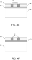
Figures 4A to 4F show the process of producing a measuring device according to another embodiment; and -
Figures 5A to 5E show the process of providing an insulating structure on another semiconductor layer of the measuring device. - Referring to
figures 1 and2 , a measuringdevice 10 according to one embodiment will be explained. The measuringdevice 10 may be used for a flow cytometer in order to perform biophysical characterization of objects such as individual cells flowing in a predefined channel, as described below by way of example. For example, the flow cytometer may be used to identify cancer cells from the samples introduced into the channel with fluid flow. The general concept of the flow cytometer is well known in the art and thus detailed explanations are omitted in the present disclosure. Nonetheless, the possible application of the measuringdevice 10 disclosed herein is not limited to characterization of individual cells. In fact, the measuringdevice 10 may also be used for characterization of other objects, including, but not being limited to, microbeads (e.g. polymer and silica), gels (e.g. DNA gels and cell culturing gels), organoids, liposomes, and exosomes. - The measuring
device 10 comprises amicrofluidic chip 20 provided with aflow channel 22 configured to allow for fluid flow that carries cells (a single cell X is schematically shown infigure 1 ) subjected to biophysical characterization. Cells are provided in the form of cell suspension or in any other forms compatible with the flow cytometry. - The
chip 20 has a silicon-based layered structure made from an SOI (Silicon on Insulator) wafer, comprising atop silicon layer 21, abottom silicon layer 25, and asilicon oxide layer 23 between the silicon layers 21 and 25. Theflow channel 22 is in the form of a cavity formed in thetop silicon layer 21. Theflow channel 22 is delimited by a pair of opposinglateral walls bottom wall 22c connecting thelateral walls - Although not illustrated, a cover layer such as a PDMS (polydimethylsiloxane) layer is fitted on the
top silicon layer 21, thereby theflow channel 22 has a substantially closed structure over an area where the biophysical characterization takes place, while allowing for required installation of the measuringdevice 10 and connections of electrical components. The cover layer may also be formed from other polymers, or another material not limited to but including glass, quartz, or other wafers with a dielectric coating. The cover layer is provided with an inlet of theflow channel 22 where the cells are introduced and an outlet of theflow channel 22 connected to a vacuum pump (not shown) for creating continuous fluid flow within theflow channel 22. - The
chip 20 also includes anelectric sensing module 30 for acquiring physical properties of the cells in theflow channel 22. The physical characteristics to be acquired by theelectric sensing module 30 are not limited to, but may include, cell size, membrane capacitance and cytoplasm resistivity. - The
electrical sensing module 30 includes at least one drivingelectrode 32 and at least onesensing electrode 34. The drivingelectrode 32 provided on thelateral wall 22a of theflow channel 22. Thesensing electrode 34 provided on thelateral wall 22b opposite thelateral wall 22a where the drivingelectrode 32 is provided. The distance between theelectrodes electrodes top silicon layer 21. Theflow channel 22 may have a relatively small width in the area where theelectrical sensing module 30 is provided in such a way that a single object, e.g. a cell, passes through at a time for the electrical characterization. - The
electrical sensing module 30 may include two or more of the drivingelectrodes 32 and two or more of thesensing electrodes 34, each drivingelectrodes 32 being operated in different driving modes. Theelectrical sensing module 30 may include one drivingelectrode 32 on thelateral wall 22a and two ormore sensing electrodes 34 provided on anotherlateral wall 22b. - Adjacent to the driving
electrodes 32 and thesensing electrodes 34,insulators 36 are provided. Theinsulators 36 adjacent to the drivingelectrodes 32 electrically isolate the drivingelectrodes 32 from each other and from the remainingtop silicon layer 21 of thechip 20. Likewise, theinsulators 36 adjacent to thesensing electrodes 34 electrically isolate thesensing electrodes 34 from each other and from the remainingsilicon layer 21. The interface between theinsulator 36 and the drivingelectrodes 32 as well as the interface between theinsulator 36 and thesensing electrode 34 is airtight to prevent fluid leakage from theflow channel 22. Theinsulators 36 may be made of any suitable material for the purpose of providing electrical insulation, including but not being limited to CYTOP (TM) or SU8. - Optionally, the chip may also comprise a
mechanical sensing module 40 for performing mechanical characterization of the cells. Themechanical sensing module 40 is integrated with thechip 20. Themechanical sensing module 40 includes amanipulator 42 and amechanical sensor 44. Themanipulator 42 may be a stationary component in the form of a narrower passage as shown infigure 1 . Themechanical sensor 44 may be a displacement sensor configured to detect displacement based on changes in capacitance in response to the individual cells flowing through themechanical sensing module 40. Theflow channel 22 is sufficiently narrow in an area where themechanical sensing module 40 is provided, whereby a cell reaching the narrow passage is subjected to deformation. Themechanical sensor 44 detects the reaction of the cells, thereby acquiring mechanical properties of the cell, including but not limited to rigidity or viscosity. Alternatively, the manipulator may also be an adjustable manipulator configured to move toward or away from the opposingmechanical sensor 44, compressing a cell flowing the passage between the mobile manipulator and themechanical sensor 44 in a controlled manner. - Optionally, the
chip 20 may have an insulating filling 27 (seefigure 2 ) in a cavity formed in thebottom silicon layer 25 over an area where theelectrical sensing module 30 is disposed, or in other words the area where the measurement takes place by theelectrical sensing module 30. - In operation, the cell suspension is introduced from the inlet of the
flow channel 22, passing through theelectrical sensing module 30 and themechanical sensing module 40 where the respective biophysical characterizations take place. - A voltage is applied between the driving
electrode 32 and thesensing electrode 34 at different frequencies, thereby generating an electric current flowing through theflow channel 22 and between theelectrodes flow channel 22 locally increases. By measuring the increased resistivity, the electrical signatures of the individual cells are acquired. The presence of the cell also affects the vertical distribution of the electrical field in the channel. - According to the measuring
device 10 having the above-described configuration, theinsulators 36 separate the drivingelectrodes 32 from each other and from thetop silicon layer 21. Therefore, a parasitic current that could possibly have been generated between them can be prevented and thus the signal quality sensed by thesensing electrode 34 is improved. - Further, the interfaces between the
electrodes insulators 36 are airtight. In other words, no slit is formed, unlike some existing devices, between the drivingelectrode 32 and the adjacent channel wall of thetop silicon layer 21 as well as between the sensingelectrode 34 and the adjacent channel wall. This ensures that introduction of the fluid into theflow channel 22 is performed efficiently because no air enters theflow channel 22 through those slits during the process of applying negative pressure at the outlet of the channel. In addition, such slits would have affected the signal quality sensed by thesensing module 34 due to parasitic signals that is to be generated between the electrodes and channel walls before and after passage of the flowing cells, in particular in case of fluid flow having a high flow rate. Therefore, the airtight structure of the present disclosure also contributes to the signal quality. - The optional formation of the insulating filling 27 in the
bottom silicon layer 25 is also advantageous to further improve the signal quality. Without the insulating filling 27 behind theoxide layer 23, thebottom silicon layer 25 would have acted as an additional electrode that captures part of the electric current otherwise flowing between theelectrodes flow channel 22. This would have affected electrical signals sensed by thesensing electrode 34, depending on the distance between the flowing cell and thebottom silicon layer 25. The presence of the insulating filling 27 prevents the dispersion in measurement result, thereby enabling trajectory-free measurement. - The insulating filling 27 also prevents electric coupling between the
top silicon layer 21 and thebottom silicon layer 25 which would have occurred in particular when theelectrical sensing module 30 is operated at a high frequency of about 10 MHz or higher. Due to the presence of the insulatingfiling 27 underneath theelectrical sensing module 30, themeasurement device 10 is operable at high frequencies without affecting in measurement result. - The optional
mechanical sensing module 40 enables integration of the system for performing the mechanical characterization of the individual cells in addition to the electrical characterization. - The measuring
device 10 thus provides single-cell impedance spectroscopy in a continuous, uninterrupted flow, thereby achieving high throughput with improved measurement accuracy. - Next, a method for producing a measuring
device 10 having the above-described configuration will be described. -
Figures 3A to 3H show the process of making a measuringdevice 10 according to one embodiment. According to the disclosed embodiment, the measuringdevice 10 in particular thechip 20 is made from an SOI (Silicon on Insulator)substrate 100. The SOI technology has been used for many years in the field of electronics and MEMS (Micro Electro Mechanical Systems) and thus well known to a person skilled in the art. - The
SOI substrate 100 comprises abottom semiconductor layer 50, anoxide layer 70 provided on thebottom semiconductor layer 50, and atop semiconductor layer 90 provided on the oxide layer 70 (figure 3A ). - Aluminum coating is then applied onto the
top semiconductor layer 90, forming a protective layer 60 (figure 3B ). - The
protective layer 60 is patterned by means of photolithography and thetop semiconductor layer 90 is patterned by means of DRIE etching (Deep Reactive Ion Etching) to form a cavity corresponding to the shapes of theflow channel 20, theelectrical sensing module 30 andgaps 92 adjacent to the electrical sensing module 30 (figure 3C ). Optionally, themechanical sensing module 40 is also provided in the process. - An insulating
material 80 such as CYTOP (TM) is applied to thegap 92 as well as onto the top of theprotective layer 60, for example, by means of deposition (figure 3D ). - Further aluminum coating is applied onto the insulating
material 80 to form a protective layer 62 (figure 3E ). - Then, the
protective layer 62 is patterned by photolithography and removed by etching, leaving a portion where thegaps 92 are formed (Seefigure 3F together withfigure 3C ). - A portion of the insulating
material 80 which is not covered by the patternedprotective layer 62 is removed, for example, by plasma etching (figure 3G ). - The remaining
protective layer 62 is then removed and the insulatingmaterial 80 underneath theprotective layer 62 is removed by plasma etching to form the insulating filling 81 having a surface substantially in flush with the top of the top semiconductor layer 90 (figure 3H ). Keeping the insulating filling 80 flush with thetop semiconductor layer 90 is advantageous since it improves adherence of the cover layer such as a PDMS cover film over the entirety of the measuringdevice 10, in particular the sensing area, thereby preventing fluid leakage from the sensing area. - According to the disclosed method, the measuring device comprising the individually polarizable electrodes and the preferred electrical isolations are produced. The method is advantageously compatible with mass production of the measuring
device 10 integrated with theelectrical sensing module 30 and optionally with themechanical sensing module 40. - Referring to
figures 4A to 4F , a method for producing the measuringdevice 10 according to another embodiment will be described. - Starting from an
SOI substrate 100, substantially the same steps are carried out as those described above with reference tofigures 3A to 3C to form thegaps 92 adjacent to the drivingelectrodes 32 and thesensing electrodes 34 of the electrical sensing module 30 (figures 4A to 4C ). - Then, a photoresist such as SU8 is applied by deposition in the
gaps 92 and on the top of the protective layer 60 (figure 4D ), to obtain aphotoresist layer 82. - The
photoresist layer 82 is patterned by photolithography to remove the portion covering the top of theprotective layer 60 to form an insulating filling 81 within the gaps 92 (figure 4E ). - Finally, the
protective layer 60 is removed to expose thetop semiconductor layer 90 underneath (figure 4F ). - This process also enjoys the same advantages as the method as described above with reference to
figures 3A to 3H . - Although the embodiments as described above involve removal of a portion of the
top semiconductor layer 90 as a result of the patterning step with reference tofigures 3C and4C , theoxide layer 70 may also be removed in order to expose thebottom semiconductor layer 50 behind theoxide layer 70. - Referring to
figures 5A to 5E , an example of the process of replacing a portion of thebottom semiconductor layer 50 of the measuringdevice 10 by an insulator will be described. - Onto the
bottom semiconductor layer 50 of the SOI substrate 100 (seefigure 4A , for example), aluminum coating is applied to form a protective layer 110 (figure 5A ). - The
protective coating 110 is patterned by photolithography to expose a portion of thebottom semiconductor layer 50 where the insulating filling is to be provided (figure 5B ). - A portion of the
first semiconductor layer 50 which was not covered by theprotective layer 110 is removed by DRIE to form cavities 112 (figure 5C ). - An insulating material, for example, PDMS, is locally deposited to the cavities 112 (
figure 5D ) to obtain an insulating filling 120 in the cavities 112 (figure 5D ). - Finally, the
protective layer 110 is removed to expose the bottom of the remaining first semiconductor layer 50 (figure 5E ). The removal of theprotective layer 110 is optional. In fact, theprotective layer 110 may remain in the measuringdevice 10, provided that theprotective layer 110 is grounded. - The method described above with reference to
figures 5A to 5E is also advantageously compatible with mass production of the measuringdevice 10 having the insulator on the side of the device opposite theelectrical sensing module 30. - According to another embodiment, the method may further involve removal of a portion of the
oxide layer 70 during the process of forming thecavities 112 in order to expose thetop semiconductor layer 90 behind theoxide layer 70. - Although some particular embodiments of the present disclosure are described above with reference to the accompanying drawings, modification, addition or omission of optional features of the embodiments may be made by the skilled person within the scope of the appended claims.
Claims (13)
- A method for producing a measuring device (10) for measuring physical characteristics of objects such as individual cells in fluid flow,the measuring device comprising a microfluidic chip (20) provided with a flow channel (22) for allowing fluid flow and an electrical sensing module (30) including at least two electrodes (32, 34) and configured to acquire a physical characteristic of an object in the fluid flow;the method comprising:preparing an SOI substrate (100) comprising a first semiconductor layer (90), a second semiconductor layer (50) and an oxide layer (70) provided between the first semiconductor layer and the second semiconductor layer,patterning at least the first semiconductor layer to form a cavity, the cavity defining lateral walls (22a, 22b) of the flow channel, a bottom wall (22c) of the flow channel connecting the lateral walls and the at least two electrodes, the cavity further defining a gap (92) adjacent to each electrode along the flow channel; andapplying an insulating material (80, 82) to each gap to form an insulating filling (81) for electrically insulating the electrical sensing module from the remaining first semiconductor layer.
- A method according to claim 1, wherein the insulating material is a non-photo-patternable material,
the applying of the insulating material further comprising:applying the insulating material to the cavity;applying a mask layer (62) onto the insulating material in the cavity;patterning the mask layer according to a contour of each gap (92); andremoving the insulating material (80) according to the patterned mask layer. - A method according to claim 1, wherein the insulating material is a photo-patternable material,
the applying of the insulating material further comprising:applying the insulating material (82) to the cavity; andremoving the insulating material in the cavity according to a contour of each gap. - A method according to any one of claims 1 to 3, wherein the insulating material is applied to each gap such that the insulating filling (81) is substantially flush with the remaining first semiconductor layer (90).
- A method according to any one of claims 1 to 4, wherein the cavity is formed to expose the oxide layer.
- A method according to any one of claims 1 to 4, wherein the cavity is formed to expose the second semiconductor layer.
- A method according to any one of claims 1 to 6, further comprising:patterning at least the second semiconductor layer (50) to form a further cavity (112) in the second semiconductor layer (50) to expose a portion of the oxide layer (70) opposite which the electrical sensing module (30) is provided, or to expose the first semiconductor layer (90); andapplying an insulating material (120) to the cavity to form an insulating filling (122) for electrically insulating the electrical sensing module from the remaining second semiconductor layer.
- A measuring device (10) for measuring physical characteristics of objects such as individual cells in fluid flow, the measuring device comprising:a microfluidic chip (20) including a flow channel (22) configured to allow for fluid flow and an electrical sensing module (30) configured to acquire a physical characteristic of an object in the fluid flow,wherein the chip comprises:a first semiconductor layer (21);a second semiconductor layer (25); andan oxide layer (23) provided between the first and second semiconductor layers,wherein the first semiconductor layer is provided with a cavity, the cavity defining lateral walls (22a, 22b) of the flow channel and a bottom wall (22c) of the flow channel connecting the lateral walls,wherein the electrical sensing module comprises:
at least two electrodes (32, 34), one (32) of the at least two electrodes being provided on one (22a) of the lateral walls of the flow channel, another (34) of the at least two electrodes being provided on the other (22b) of the lateral walls of the flow channel,the measuring device being characterized by further comprisingan insulating filing (36) provided adjacent to each electrode along the flow channel and configured to electrically isolate each electrode from the first semiconductor layer (21). - A measuring device according to claim 8, wherein the electrical sensing module (30) comprises at least four electrodes, the insulating fillings (36) being configured to electrically isolate the electrodes from each other.
- A measuring device according to claim 8 or 9, wherein an interface between each electrode and the adjacent insulating material is airtight.
- A measuring device according to any one of claims 8 to 10, wherein the second semiconductor layer (25) is provided with a further cavity filled with an insulating filling (27) that is in contact with the oxide layer (23) opposite the first semiconductor layer (21) or in direct contact with the first semiconductor layer (21).
- A measuring device according to any one of claims 8 to 11, further comprising a mechanical sensing module (40) spaced apart from the electrical sensing module (30) along the flow channel (22) and configured to acquire a mechanical characteristic of the object in the fluid flow.
- A measuring device according to claim 12, wherein the mechanical sensing module (40) comprises a manipulator provided on one of the lateral walls of the flow channel and a sensor provided on the other of the lateral walls of the flow channel.
Priority Applications (2)
| Application Number | Priority Date | Filing Date | Title |
|---|---|---|---|
| EP22307000.4A EP4390367A1 (en) | 2022-12-22 | 2022-12-22 | Measuring device and method for producing measuring device |
| PCT/EP2023/087374 WO2024133754A1 (en) | 2022-12-22 | 2023-12-21 | Measuring device and method for producing measuring device |
Applications Claiming Priority (1)
| Application Number | Priority Date | Filing Date | Title |
|---|---|---|---|
| EP22307000.4A EP4390367A1 (en) | 2022-12-22 | 2022-12-22 | Measuring device and method for producing measuring device |
Publications (1)
| Publication Number | Publication Date |
|---|---|
| EP4390367A1 true EP4390367A1 (en) | 2024-06-26 |
Family
ID=85018739
Family Applications (1)
| Application Number | Title | Priority Date | Filing Date |
|---|---|---|---|
| EP22307000.4A Pending EP4390367A1 (en) | 2022-12-22 | 2022-12-22 | Measuring device and method for producing measuring device |
Country Status (2)
| Country | Link |
|---|---|
| EP (1) | EP4390367A1 (en) |
| WO (1) | WO2024133754A1 (en) |
Citations (1)
| Publication number | Priority date | Publication date | Assignee | Title |
|---|---|---|---|---|
| WO2021069446A1 (en) | 2019-10-08 | 2021-04-15 | Centre National De La Recherche Scientifique (Cnrs) | Measuring device and method for measuring characteristics of cells |
-
2022
- 2022-12-22 EP EP22307000.4A patent/EP4390367A1/en active Pending
-
2023
- 2023-12-21 WO PCT/EP2023/087374 patent/WO2024133754A1/en not_active Ceased
Patent Citations (1)
| Publication number | Priority date | Publication date | Assignee | Title |
|---|---|---|---|---|
| WO2021069446A1 (en) | 2019-10-08 | 2021-04-15 | Centre National De La Recherche Scientifique (Cnrs) | Measuring device and method for measuring characteristics of cells |
Non-Patent Citations (15)
| Title |
|---|
| B. LEGRANDA. E. ASHCROFTL. BUCHAILLOTS. ARSCOTT: "SOI-based nanoelectrospray emitter tips for mass spectrometry: a coupled MEMS and microfluidic design", J. MICROMECH. MICROENG., vol. 17, no. 3, 6 February 2007 (2007-02-06), pages 509 - 514, XP020120028, DOI: 10.1088/0960-1317/17/3/013 |
| C. ADAMOPOULOSA. GHARIAA. NIKNEJADV. STOJANOVICM. ANWAR: "Microfluidic Packaging Integration with Electronic-Photonic Biosensors Using 3D Printed Transfer Molding", BIOSENSORS (BASEL, vol. 10, no. 11, 14 November 2020 (2020-11-14) |
| C. HONRADOP. BISEGNAN. S. SWAMIF. CASELLI: "Single-cell microfluidic impedance cytometry: from raw signals to cell phenotypes using data analytics", LAB CHIP, vol. 21, 2021, pages 22 - 54 |
| E. ROLLO ET AL.: "Label-free identification of activated T lymphocytes through tridimensional microsensors on chip", BIOSENSORS AND BIOELECTRONICS, vol. 94, 15 August 2017 (2017-08-15), pages 193 - 199, XP029983737, DOI: 10.1016/j.bios.2017.02.047 |
| GAWAD SSUN TGREEN NGMORGAN H: "Impedance spectroscopy using maximum length sequences: Application to single cell analysis", REV SCI INSTRUM, vol. 78, 2007, pages 054301 |
| PETCHAKUP, C.LI, K.H.H.HOU, H.W.: "Advances in Single Cell Impedance Cytometry for Biomedical Applications", MICROMACHINES, vol. 8, 2017, pages 87 |
| Q. REZARDG. PERRETJ.C. GERBEDOEN ET AL., IEEE INT. CONF. ON MEMS (MEMS'21, 2021, pages 494 |
| R. REALEA. DE NINNOL. BUSINAROP. BISEGNAF. CASELLI: "High-throughput electrical position detection of single flowing particles/cells with non-spherical shape", LAB CHIP, vol. 19, no. 10, 14 May 2019 (2019-05-14), pages 1818 - 1827, XP055801985, DOI: 10.1039/C9LC00071B |
| REZARD QUENTIN ET AL: "Developing A Mems Device for High-Throughput Multi-Parameter Single Cell Biophysical Analysis", 2021 IEEE 34TH INTERNATIONAL CONFERENCE ON MICRO ELECTRO MECHANICAL SYSTEMS (MEMS), IEEE, 25 January 2021 (2021-01-25), pages 494 - 497, XP033887023, DOI: 10.1109/MEMS51782.2021.9375176 * |
| S. GAWADL. SCHILDP. RENAUD: "Micromachined impedance spectroscopy flow cytometer for cell analysis and particle sizing", LAB ON A CHIP, vol. 1, no. 1, 2001, pages 76 - 82, XP008028057, DOI: 10.1039/b103933b |
| S. M. WEIZM. MEDINA-SANCHEZO. G. SCHMIDT: "Microsystems for Single-Cell Analysis", ADVANCED BIOSYSTEMS, vol. 2, no. 2, 2018 |
| S. SHARMAK. BUCHHOLZS. M. LUBERU. RANTM. TORNOWG. ABSTREITER: "Silicon-on-Insulator Microfluidic Device With Monolithic Sensor Integration for MicroTAS Applications", JOURNAL OF MICROELECTROMECHANICAL SYSTEMS, vol. 15, no. 2, pages 308 - 313 |
| T. CHINGFUH. CHENGHAN: "Thermal Bubble Microfluidic Gate Based on SOI Wafer", JOURNAL OF MICROELECTROMECHANICAL SYSTEMS, vol. 18, no. 4, 2009, pages 852 - 859, XP011269839, DOI: 10.1109/JMEMS.2009.2023882 |
| TAKAYAMA YUKI ET AL: "Developing a MEMS Device with Built-in Microfluidics for Biophysical Single Cell Characterization", MICROMACHINES, vol. 9, no. 6, 1 June 2018 (2018-06-01), pages 275, XP093021813, DOI: 10.3390/mi9060275 * |
| X. HUANG ET AL.: "Self-aligned sequential lateral field non-uniformities over channel depth for high throughput dielectrophoretic cell deflection", LAB CHIP, vol. 21, no. 5 |
Also Published As
| Publication number | Publication date |
|---|---|
| WO2024133754A1 (en) | 2024-06-27 |
Similar Documents
| Publication | Publication Date | Title |
|---|---|---|
| EP3001862B1 (en) | Mems pressure sensors with integrated baffles | |
| Koch et al. | Design and fabrication of a micromachined Coulter counter | |
| Sun et al. | A bulk microfabricated multi-axis capacitive cellular force sensor using transverse comb drives | |
| CN102401706B (en) | MEMS pressure sensor part and manufacture method thereof | |
| US7114397B2 (en) | Microelectromechanical system pressure sensor and method for making and using | |
| JP2003527581A (en) | Apparatus and method for electrical measurement of an object | |
| US10730741B2 (en) | MEMS sensor, especially pressure sensor, for metrological registering of a measured variable | |
| CN101661012A (en) | Microfilm capacitive type surface stress sensor used for biochemical detection and manufacture method thereof | |
| CN115541099A (en) | Capacitive microfluidic pressure sensor, preparation method and microfluidic chip thereof | |
| US20140340093A1 (en) | Liquid ion detector | |
| CN102520147B (en) | Capacitive micromachined ultrasonic transducer (CMUT) for detecting trace biochemical substances and preparation method for CMUT | |
| US12292372B2 (en) | Measuring device and method for measuring characteristics of cells | |
| WO2005100953A2 (en) | Microfluidic system | |
| WO2024133754A1 (en) | Measuring device and method for producing measuring device | |
| CN112683348A (en) | MEMS capacitive flow sensor and preparation method thereof | |
| EP3508844B1 (en) | Ion sensor, ion sensor manufacturing method, and field asymmetric ion mobility spectrometry system | |
| US20140008224A1 (en) | Method and microsystem for detecting analytes which are present in drops of liquid | |
| US8323955B1 (en) | Micromachined patch-clamp apparatus | |
| CN117705313B (en) | MEMS capacitive temperature and humidity integrated sensor and preparation method thereof | |
| KR102186264B1 (en) | Open microfluidic channel integrated biosensor and manufacturing method the same | |
| Bonnema et al. | Flow-through microfluidic relative permittivity sensor using highly-doped silicon sidewall electrodes | |
| EP3882580B1 (en) | Method for manufacturing a silicon-based coriolis-force-based flow sensing device | |
| US11906416B2 (en) | MEMS microparticle sensor | |
| EP1196349A1 (en) | Micro-electromechanical devices and methods of manufacture | |
| Hediger et al. | Fabrication of a novel microsystem for the electrical characterisation of cell arrays |
Legal Events
| Date | Code | Title | Description |
|---|---|---|---|
| PUAI | Public reference made under article 153(3) epc to a published international application that has entered the european phase |
Free format text: ORIGINAL CODE: 0009012 |
|
| STAA | Information on the status of an ep patent application or granted ep patent |
Free format text: STATUS: THE APPLICATION HAS BEEN PUBLISHED |
|
| AK | Designated contracting states |
Kind code of ref document: A1 Designated state(s): AL AT BE BG CH CY CZ DE DK EE ES FI FR GB GR HR HU IE IS IT LI LT LU LV MC ME MK MT NL NO PL PT RO RS SE SI SK SM TR |
|
| STAA | Information on the status of an ep patent application or granted ep patent |
Free format text: STATUS: REQUEST FOR EXAMINATION WAS MADE |
|
| 17P | Request for examination filed |
Effective date: 20241223 |
|
| STAA | Information on the status of an ep patent application or granted ep patent |
Free format text: STATUS: EXAMINATION IS IN PROGRESS |
|
| 17Q | First examination report despatched |
Effective date: 20250722 |