EP4390349A1 - Thermal impedance monitoring process for power modules - Google Patents
Thermal impedance monitoring process for power modules Download PDFInfo
- Publication number
- EP4390349A1 EP4390349A1 EP22306944.4A EP22306944A EP4390349A1 EP 4390349 A1 EP4390349 A1 EP 4390349A1 EP 22306944 A EP22306944 A EP 22306944A EP 4390349 A1 EP4390349 A1 EP 4390349A1
- Authority
- EP
- European Patent Office
- Prior art keywords
- frequency
- thermal impedance
- monitoring process
- die
- thermal
- Prior art date
- Legal status (The legal status is an assumption and is not a legal conclusion. Google has not performed a legal analysis and makes no representation as to the accuracy of the status listed.)
- Granted
Links
Images




Classifications
-
- G—PHYSICS
- G01—MEASURING; TESTING
- G01K—MEASURING TEMPERATURE; MEASURING QUANTITY OF HEAT; THERMALLY-SENSITIVE ELEMENTS NOT OTHERWISE PROVIDED FOR
- G01K7/00—Measuring temperature based on the use of electric or magnetic elements directly sensitive to heat ; Power supply therefor, e.g. using thermoelectric elements
- G01K7/42—Circuits effecting compensation of thermal inertia; Circuits for predicting the stationary value of a temperature
- G01K7/427—Temperature calculation based on spatial modeling, e.g. spatial inter- or extrapolation
-
- H—ELECTRICITY
- H02—GENERATION; CONVERSION OR DISTRIBUTION OF ELECTRIC POWER
- H02M—APPARATUS FOR CONVERSION BETWEEN AC AND AC, BETWEEN AC AND DC, OR BETWEEN DC AND DC, AND FOR USE WITH MAINS OR SIMILAR POWER SUPPLY SYSTEMS; CONVERSION OF DC OR AC INPUT POWER INTO SURGE OUTPUT POWER; CONTROL OR REGULATION THEREOF
- H02M1/00—Details of apparatus for conversion
- H02M1/32—Means for protecting converters other than automatic disconnection
- H02M1/327—Means for protecting converters other than automatic disconnection against abnormal temperatures
-
- H—ELECTRICITY
- H02—GENERATION; CONVERSION OR DISTRIBUTION OF ELECTRIC POWER
- H02M—APPARATUS FOR CONVERSION BETWEEN AC AND AC, BETWEEN AC AND DC, OR BETWEEN DC AND DC, AND FOR USE WITH MAINS OR SIMILAR POWER SUPPLY SYSTEMS; CONVERSION OF DC OR AC INPUT POWER INTO SURGE OUTPUT POWER; CONTROL OR REGULATION THEREOF
- H02M7/00—Conversion of AC power input into DC power output; Conversion of DC power input into AC power output
- H02M7/42—Conversion of DC power input into AC power output without possibility of reversal
- H02M7/44—Conversion of DC power input into AC power output without possibility of reversal by static converters
- H02M7/48—Conversion of DC power input into AC power output without possibility of reversal by static converters using discharge tubes with control electrode or semiconductor devices with control electrode
- H02M7/53—Conversion of DC power input into AC power output without possibility of reversal by static converters using discharge tubes with control electrode or semiconductor devices with control electrode using devices of a triode or transistor type requiring continuous application of a control signal
- H02M7/537—Conversion of DC power input into AC power output without possibility of reversal by static converters using discharge tubes with control electrode or semiconductor devices with control electrode using devices of a triode or transistor type requiring continuous application of a control signal using semiconductor devices only, e.g. single switched pulse inverters
- H02M7/5387—Conversion of DC power input into AC power output without possibility of reversal by static converters using discharge tubes with control electrode or semiconductor devices with control electrode using devices of a triode or transistor type requiring continuous application of a control signal using semiconductor devices only, e.g. single switched pulse inverters in a bridge configuration
- H02M7/53871—Conversion of DC power input into AC power output without possibility of reversal by static converters using discharge tubes with control electrode or semiconductor devices with control electrode using devices of a triode or transistor type requiring continuous application of a control signal using semiconductor devices only, e.g. single switched pulse inverters in a bridge configuration with automatic control of output voltage or current
-
- G—PHYSICS
- G01—MEASURING; TESTING
- G01K—MEASURING TEMPERATURE; MEASURING QUANTITY OF HEAT; THERMALLY-SENSITIVE ELEMENTS NOT OTHERWISE PROVIDED FOR
- G01K2217/00—Temperature measurement using electric or magnetic components already present in the system to be measured
Definitions
- the present disclosure is in the field of protecting power semiconductor modules from failures due to overheating in particular overheating due to thermal interfaces degradation and maintenance of equipment using such modules.
- Thermal interfaces degradation in a power module is due to delamination and void creation in any of the substructures between a semiconductor die and a heatsink. These degradations increase temperature of the semiconductor die that can lead to an unsafe temperature operation region. The consequence of the high temperature is the semiconductor breakdown and power module failure. Monitoring the thermal interfaces is then important to maintain the power module in a safe temperature region and guide maintenance and replacement phases of the power module.
- the degradation phenomena are caused by the temperature swing and the CTE mismatch between the different materials composing a power module stack-up shown in figure 1 that includes at least: semiconductor die 3 (for example in silicon), die attach 4 (for example in solder), a conductive layer 6 (for example in copper), an electrical insulator layer 7, and a heat-sink 8 (for example in aluminum).
- semiconductor die 3 for example in silicon
- die attach 4 for example in solder
- a conductive layer 6 for example in copper
- an electrical insulator layer 7 for example in aluminum
- the power module 1 can also comprise elements such : a thermal conductive layer 9 (for example in copper), a join layer 10 (for example solder), a base plate 11 (for example copper), a thermal interface 12 (for example graphite or thermal paste).
- a thermal conductive layer 9 for example in copper
- a join layer 10 for example solder
- a base plate 11 for example copper
- a thermal interface 12 for example graphite or thermal paste.
- a symmetric material stack-up can be also envisaged in the case of a double side cooling where the stack-up present hereinbefore is repeated on the top side 5 of the semiconductor die 3.
- Figure 2 shows possible cracks 2 in a layer such as layer 4. Such cracks cause a reduction of the thermal conduction of the layer.
- the standard JESD51-14 describe a method to measure the 'transient measurement of thermal resistance'.
- the method consists of measuring the junction temperature preferably after the heating power is switched off (cooling curve).
- the heating curve can be used if there is a constant heating power during the heating pulse time.
- the measurement obliges the power module to be turned-off after being worked in a known and thermal steady-state condition.
- the power losses should be known, which is hardily estimated during the on-line operation (in field application).
- Thermal impedance measurements techniques are powerful transient thermal response techniques which can give information on the degradation of the different interfaces of the power module.
- the technique typically consists in:
- the lock-in thermography techniques uses a process where the material or system to be analyzed thermally is excited with a non-steady state signal (e.g a pulsed signal, or a sinusoidal signal) at a specific frequency (related to the material thickness or damage depth), for example using an infrared radiative source such as a set of halogen lamps, recording images of the transient temperature response of the system/material, using specific software and algorithm, calculating the phase and the amplitude between the response and the excitation, and thus generating a phase image and an amplitude image.
- a non-steady state signal e.g a pulsed signal, or a sinusoidal signal
- an infrared radiative source such as a set of halogen lamps
- the present disclosure proposes a measurement method using a lock-in technique in transient states instead of steady state situations.
- the present disclosure proposes a thermal impedance monitoring process for a power module of a power converter used for transforming DC current to AC current, or vice-versa, where the semiconductor dissipates an asymmetrical loss between two half cycles of an AC frequency f of the AC current, said power module comprising at least a semiconductor die attached to a material stack-up of layers for its thermal dissipation and/or electrical connections, said process comprising:
- the process may comprise measuring said AC frequency and storing couple of time duration ⁇ t tx and AC frequency, f fund values.
- the signal relating to the junction temperature Tj may be a temperature sensitive electrical parameter of said semiconductor.
- the signal may be a non-calibrated temperature sensitive electrical parameter of said semiconductor.
- Said AC frequency may be lower than 2kHz.
- Said AC frequency may be lower than 1kHz.
- Said AC frequency may be the fundamental frequency powering the converter or the fundamental output frequency f fund of the converter.
- the present disclosure concerns also a converter comprising sensor means on a power semiconductor switch die of said converter for sensing a temperature on said power semiconductor switch die, analog to digital converter means, sampling means and a processor provided with memory means for storing and running a software configured for executing the thermal impedance monitoring process described hereabove.ln particular, said sensor means may be designed to sense a temperature sensitive electrical parameter of said die.
- the present disclosure proposes also a software comprising instructions for executing the thermal impedance monitoring process disclosed hereabove.
- the reflection coefficient is function of the material properties and of the contact resistance between the different materials, in case voids or defects are present at the interface.
- the reflection coefficient is also frequency dependent.
- the curves in figure 3 show the effect of a defect of strength R positioned a depth d on the phase shift of the surface temperature response as disclosed in document Rigert "Indutechnischs-Lockin-Therm conducting : ein Hallmaschine Kunststoff zermetsenfintechnik march” http://dx.doi.org/10.18419/opus-1734.
- the surface temperature response phase shift changes from the semi-infinite body value of 45° to a lower value that depends on R and on the position of the defect.
- Figure 3 thus shows the basic principle of lock-in thermography to characterize defects and interfaces in materials, devices including a module stack-up.
- ⁇ is frequency dependent: for defects located further into the material, greater sensitivity is obtained when lower excitation frequency is used.
- the excitation frequency information about interface (degradation) of different layer stack or interface can be gained.
- Thermal impedance electrical equivalent model: On the basis that heat conduction and electronic conduction are both physical processes modelled by the same phenomenon (diffusion), the thermal impedance of a semiconductor module can be modelled by analogy with the scaled heat conduction equation and the telegrapher's equations. Thus, an equivalent electrical network of the thermal system can be deduced.
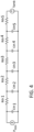
- an electrical network can represent the thermal system of a stack-up of 5 layers as shown in Erreur ! Source du rijn introuvable.
- P loss is the heat flux from the semiconductor die 5 of figure 1 , corresponding to the losses dissipated on the semiconductor die (the electrical equivalent is a current source)
- C th and R th are the equivalent capacitance and resistance of each layer starting with the die layer 3 and the heatsink layer 5
- Tamb is the environment heatsink temperature.
- Table 1 Stack up layers ⁇ W/mK ⁇ g/cm 3 c J/gK l mm 3 (silicon) 80 2,3 0,7l2 0,l4 4 (die attach) 50 7,4 0,24 0,l 6 404 8,9 0,385 0,3 7 l60 3,3 0,72 0,7 9 450 8,9 0,385 0,32 l0 60 7,4 0,24 0,4 ll 450 8,9 0,385 4 l2 30 l,8l 0,85 0,l5 8 239 2,7 0,92l 20
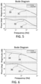
- the thermal impedance may be plotted in a bode diagram, where the amplitude and the phase are plotted in function of the excitation frequency of a sinus type.
- a comparison is done between a pristine, that is non-degraded module, and a degraded module according to figure 1 with measurements done at increasing frequencies.
- Figure 5 is the Bode diagram of a stack according to figure 1 with the layer 4 and the layer 10 having 40% of voids.
- Figure 6 is the Bode diagram of a stack according to figure 1 with the layer 4 has 40% of voids.
- Figure 7 is the Bode diagram of a stack according to figure 1 with the layer 10 has 40% of voids.
- Curves 32, 33 of figure 5 , curves 36, 37 of figure 6 and curves 40, 41 of figure 7 are representing the phase difference between the temperature variations of the die for of pristine in dotted line and degraded layers in plain lines.
- Curves 30, 31 of figure 5 , curves 34, 35 of figure 6 and curves 38, 39 of figure 7 are representing the amplitude of the temperature variation of the die with pristine in dotted line and degraded layers in plain lines.
- typical signal modulation strategies such as PWM modulation in converters typically operate at frequencies higher than 1kHz, such as 5kHz, or 10kHz.
- the thermal system response will be weak in this frequency range, and the temperature oscillations due to the PWM frequency will be weak as seen in the magnitude of the bode plot ⁇ -60dB of figure 8 .
- the thermal system will not be influenced by the PWM excitation. For the use of the model described in the previous section this justifies that the losses can be averaged over a PWM period.
- typical excitation frequencies may be limited by the load impedance, by the load requirements, or by the external control of the system, such that the system is typically excited in the frequency range of interest, i.e., at a frequency lower than 1kHz, for example 50Hz, 60Hz, 100Hz, 400Hz, or 1 Hz.
- a low frequency electrical excitation signal should not decrease from the maximum power value to the zero-power value within a time interval lower than ⁇ d .
- the power semiconductor die losses waveform is dependent on the application where the power module or system is installed.
- This invention relates to the cases of DC/AC or AC/DC power converter topologies, and to the cases where the losses are low frequency periodic pulsating waves with the following characteristics:
- FIG 9 An example of DC/AC power topology is shown in figure 9 where a DC supply 51 serves to build a three-phase alternating supply 52 using power semiconductor switches 1.
- the DC/AC power converter has a 3-phase configuration supplied by a DC bus voltage.
- the semiconductor die can be any IGBT, Diode, MOSFET, MISFET and in any placement of the power converter topology.
- the semiconductor die of interest in the power module is placed in one leg at the high side position.
- the switching and conduction losses of the semiconductor die 50 are generated in a normal operation of the power module in a motor control application given the load current, the bus voltage during the switching and conduction events.
- the semiconductor die losses generation in a power module on a DC/AC or DC/AC operation is proportional to the following variables that are related to the operating point: the current passing through I cond , the switched current I sw , the switched voltage V sw , the switching frequency f sw , the junction temperature, T j , the duty cycle modulation strategy / PWM technique.
- a periodic pulsed loss waveform in an DC/AC or AC/DC application is generated in the fundamental frequency, e.g., a grid frequency 50Hz or an electrical motor rotation control frequency of 1Hz - 2kHz.
- the losses on the semiconductor are generated only during a time corresponding to a first half-cycle of the fundamental frequency, and the semiconductor does not generate any losses during the second half cycle of the fundamental frequency.
- the power converter generates a sinusoidal current waveform, at the fundamental frequency of 100Hz, on the output of the phases ABC and a chopped voltage waveform at the switching frequency operation of 20kHz.
- Figures 10A and 10B are representation of the junction temperature and losses for a pristine and degraded power module at 100Hz of fundamental AC frequency.
- Figure 10A is a general view of the power and junction temperature waves with respect to time
- Figure 10B is a zoomed figure on one loss period comprising also a measurement of the die temperature Tj duration time.
- the losses wave 70 in figure 10A on the semiconductor die has only the positive sinusoidal shape.
- the losses follow a sinusoidal shape between 0° and 180° (0 and ⁇ ) and have a null value between 180° and 360° ( ⁇ and 2 ⁇ ) within the fundamental frequency f f : P ⁇ ⁇ A ⁇ s 2 ⁇ ⁇ f f ⁇ t 2 f 0 ⁇ 2 ⁇ ⁇ f f ⁇ t ⁇ ⁇ 0 f ⁇ ⁇ 2 ⁇ ⁇ f f ⁇ t ⁇ 2 ⁇
- the temperature response Tj of the die 71, 72 in figure 10A is calculated using the thermal impedance.
- the temperature wave has one minimum 71a, 72a and one maximum 71b, 72b within a fundamental period.
- When measuring the time between the minimum temperature point and the maximum temperature point gives an indicator of the module degradation.
- Figure 11 shows the losses in the fundamental frequency of the converter plotted for different modulation strategies when a DC/AC power converter drives an electrical motor.
- the different modulation strategies are: Sine 60, DPWM1 61, DPWM3 62, Spacevector 63.
- the losses are calculated considering both the conduction losses and the switching losses of the semiconductor die, and averaged over a modulation period.
- the topologies of the converter are not limited to the converter taken as an example but could be multilevel topologies as the NPC (neutral point clamped inverter), ANPC (Active-neutral-point-clamped inverter), MMC (modular multilevel converter), FC (flying capacitor) and other topologies that are the state of art.
- the thermal degradation estimation is not sensitive to the accuracy of the junction temperature measurement, and thus any signal related to the temperature of the semiconductor can be used, provided there is a monotonous relation between the temperature and the signal. It is not necessary to estimate or measure the power losses in the semiconductor, thus advantageously reducing the number of sensors, the computation time and increasing the accuracy of the degradation measurement.
- the fundamental frequency f fund at which the losses are measured may be measured and stored and the degradation state is determined by the time duration ⁇ t(f fund ) at said fundamental frequency.
- the fundamental loss frequency can be measured using the AC load current probe, or be given by the controller reference, or be given by the user AC frequency request.
- damages at different height in the stack causes different phase shift in the temperature increase curves and measuring damage indicators ⁇ ti(f fund,i ) at different frequencies f fund,i enables to gain information on the degradation evolution at different layers of the stack.
- the higher frequencies are used to monitor a degradation of the stack layers closer to the semiconductor and the lower frequencies are used to monitor a degradation of the stack layers farther from the semiconductor.
- the effect of the degradation on the frequency response functions for a specific layer of the stack can be determined by introducing a degradation in a specific layer, for example using equation 4, measuring the phase shift associated with this degradation using the Z(s) estimation of equation 3, and plotting a bode diagram as in figures 5 to 7.
- one or several frequencies between 20Hz to 500Hz are used to monitor the degradation on the layer 4 according to Figure 6 and one or several frequencies between 1Hz to 10Hz are used to monitor the layer 10 resulting in the curve of figure 7.
- monitoring of the time delay at several frequencies enables to separate the contributions of the several degradations as in the example of figure 5.
- Figure 12 shows a comparison of first-order estimation of the phase Ph using equation (8), and the phase extracted from calculations using the impedance method with respect to the fundamental frequency.
- curve 80 is the estimated phase curve for degraded layers 4 and 10 of figure 1 while curve 81 is the theoretical curve for such degraded layers
- curve 82 is the estimated phase curve for degraded layer 4 while curve 83 is the theoretical curve fir such degraded layer
- curve 84 is the estimated phase curve for degrade layer 10
- curve 85 the theoretical curve for such degraded layer 10.
- the process may monitor the time difference for different fundamental frequencies. This gives a possibility to provide estimation of which of the layers are degraded layers.
- this allows to record the fundamental frequency without using an additional sensor, or without acquiring the fundamental frequency information from a separate algorithm.
- the algorithm for degradation analysis can work independently of a control algorithm of the converter or any other operating condition of the power module.
- the signal used for measuring the temperature may be any thermal sensitive electrical parameter (TSEP) of the concerned semiconductor switch.
- TSEP thermal sensitive electrical parameter
- the deterioration can be identified and quantified without any complex prior TSEP calibration, reducing the complexity of the system.
- the TSEP it is not necessary to calibrate the TSEP, i.e., to determine A and B before implementing the method since only the variable X is measured.
- A>0 and the moments tTjmax and tTjmin where the junction temperature is at the maximum correspond to the moments where X is at the maximum, respectively at the minimum value.
- a ⁇ 0 and the moments tTjmax and tTjmin where the junction temperature is at the maximum correspond to the moments where X is at the minimum, respectively at the maximum value.
- Step 100 may also comprise measuring said AC frequency and step 120 may comprise storing couple of time duration ⁇ t tx and AC frequency, f fund values.
- Measuring in step 100 may be done with several means such as thermocouple, infrared image, TSEP etc.
- averaging of the ⁇ t values may be required and the comparison may not be done strictly with the first ⁇ t 0 value measured, but rather with a mean value over a measurement period of a few alternances at the beginning of the product usage. In such case, the averaging may be done on about two to ten alternances.
- Repetition of the sampling, measuring and the comparison maybe done on a regular basis that is every day, week, month or after a number of alternances of the AC frequency corresponding to the use of the converter (e.g., tenth or hundreds of hours) relevant with the estimated degradation rate.
- Repetition rate may also be accelerated when a difference between ⁇ t tx and ⁇ t 0 becomes larger than a predetermined warning value.
- repetition of the sampling, measuring and the comparison maybe done on a regular basis that is every day, week, month or after a number of alternances of the AC frequency corresponding to the use of the converter (e.g., tenth or hundreds of hours) relevant with the estimated degradation rate.
- Repetition rate may also be accelerated when a difference between ⁇ t tx and ⁇ t 0 becomes larger than a predetermined warning value.
- tests using adaptation of the AC freqeuncy may be done in specific situations such as tests on the grid frequency or ramping of a motor speed.
- the converter as shown in figure 9 may comprise sensor means 53 on a power semiconductor switch die of said converter for sensing a TSEP signal of said power semiconductor switch die, analog to digital converter means 54, sampling means 55 and a processor 56 provided with the necessary memory means 57 and computing means for storing and running a software configured for executing the thermal impedance monitoring process of the present disclosure.
Landscapes
- Engineering & Computer Science (AREA)
- Power Engineering (AREA)
- Physics & Mathematics (AREA)
- General Physics & Mathematics (AREA)
- Testing Of Individual Semiconductor Devices (AREA)
- Power Conversion In General (AREA)
- Inverter Devices (AREA)
Abstract
- sampling and measuring a signal relating to the junction temperature Tj of said semiconductor die at a frequency higher than twice said AC frequency of said AC current,
- calculating a time duration Δt= tTjmax- tTjmin between a moment tTjmax, where said junction temperature of said semiconductor die is at a maximum value, and a moment tTjmin, where said junction temperature is at a minimum value, in one period of said AC current, and storing said time duration Δt in a memory,
- repeating said sampling and measuring said signal and said calculating said time duration at different times tx=t0 to tm during the operating life of the power module to provide a series of time durations Δtt0 to Δttm and comparing said time durations Δtt0 to Δttm values for monitoring an evolution of said time duration Δt to determine an evolution of degradation of the thermal impedance of said power module.
Description
- The present disclosure is in the field of protecting power semiconductor modules from failures due to overheating in particular overheating due to thermal interfaces degradation and maintenance of equipment using such modules.
- Thermal interfaces degradation in a power module is due to delamination and void creation in any of the substructures between a semiconductor die and a heatsink. These degradations increase temperature of the semiconductor die that can lead to an unsafe temperature operation region. The consequence of the high temperature is the semiconductor breakdown and power module failure. Monitoring the thermal interfaces is then important to maintain the power module in a safe temperature region and guide maintenance and replacement phases of the power module.
- The degradation phenomena are caused by the temperature swing and the CTE mismatch between the different materials composing a power module stack-up shown in
figure 1 that includes at least: semiconductor die 3 (for example in silicon), die attach 4 (for example in solder), a conductive layer 6 (for example in copper), anelectrical insulator layer 7, and a heat-sink 8 (for example in aluminum). - The
power module 1, can also comprise elements such : a thermal conductive layer 9 (for example in copper), a join layer 10 (for example solder), a base plate 11 (for example copper), a thermal interface 12 (for example graphite or thermal paste). A symmetric material stack-up can be also envisaged in the case of a double side cooling where the stack-up present hereinbefore is repeated on thetop side 5 of thesemiconductor die 3. -
Figure 2 showspossible cracks 2 in a layer such aslayer 4. Such cracks cause a reduction of the thermal conduction of the layer. - In document Broeck & al. "In situ thermal impedance spectroscopy of Power electronic modules for localized degradation identification", PCIM Europe 2019; International Exhibition and Conference for Power Electronics, Intelligent Motion, Renewable Energy and Energy Management, 07-09 May 2019 Nuremberg, Germany; VDE ISBN:978-3-8007-4938-6, is disclosed a method to extract the thermal impedance frequency response function of power modules without interrupting normal converter operations. A sinusoidal small-signal loss excitation to a power device, extracts the temperature response of such power device and correlates both signals to estimate the thermal impedance at the excitation frequency. The method relies on phase information rather than magnitude, and thus is insensitive to measurement errors in loss and/or temperatures. It requires a small signal loss excitation method that will impact on torque ripple for a motor driver application for example.
- In document Polom & al., "Real-Time, In Situ Degradation Monitoring in Power Semiconductor Converters" 2019 IEEE Applied Power Electronics Conference and Exposition (APEC) , 17-21 March 2019, IEEE, DOI: 10.1109/APEC.2019.872182 the spatiotemporal dynamic thermal response of a semiconductor assembly response change with degradation is measured with a heat injection having a certain frequency content (sinus and square). The temperature of the semiconductor die is estimated via TSEP (thermal sensitive electrical parameter), the frequency response function (FRF) is computed for each system identification experiment, the FRF segments are combined and a function model is interpreted for thermal interface degradation.
- In the document Xiang & al., "Condition Monitoring Power Module Solder Fatigue Using Inverter Harmonic Identification ", IEEE Transactions on Power Electronics, Volume: 27, Issue: 1, January 2012 Pages 235 - 247, DOI: 10.1109/TPEL.2011.2160988, a method to monitor solder fatigue in an inverter applying IGBT power module is described to detect the change of the output harmonic. It is shown that low-order harmonics, caused by nonideal switching, are affected by the device junction temperature, which in turn depends upon module solder condition. The method lacks on accuracy; thus, the inverter controller is set to cause harmonic resonance at a given frequency.
- The standard JESD51-14 describe a method to measure the 'transient measurement of thermal resistance'. The method consists of measuring the junction temperature preferably after the heating power is switched off (cooling curve). Although not recommended, in principle also the heating curve can be used if there is a constant heating power during the heating pulse time. In the first case, the measurement obliges the power module to be turned-off after being worked in a known and thermal steady-state condition. In both cases, the power losses should be known, which is hardily estimated during the on-line operation (in field application).
- Thermal impedance measurements techniques are powerful transient thermal response techniques which can give information on the degradation of the different interfaces of the power module. The technique typically consists in:
- First, applying a starting steady-state thermal condition on the power module using the semiconductor switch as active devices. This starting condition can either be a zero-power condition, or a condition where a known and measured constant power is dissipated at the semiconductor.
- Second, applying a controlled power step increase (in case the start condition is a zero-power condition) or a power step decrease (in case the start condition is a constant power condition), and then recording the evolution of the semiconductor temperature until the new steady state thermal condition is reached.
- Finally, the recorded temperature transient behavior is described by using an equivalent Foster and Cauer network which represent the thermal structure of the power module by several RC elements. A fitting of the temperature transient using the foster equation allow to extract the resistances and capacitances of the different part of the power module, giving information of the evolution of thermal resistances and capacitances.
- Lock-in thermography techniques are well-proven commercially available techniques to detect material and system damages (e.g. delamination cracks in composites, voids, etc...) as discussed in Gerd Busse "Lockin-Thermography: Principles", NDE-applications and trends, January 2014 Conference: 2014 Quantitative InfraRed Thermography, DOI:10.21611/qirt.2014.e.
- The lock-in thermography techniques uses a process where the material or system to be analyzed thermally is excited with a non-steady state signal (e.g a pulsed signal, or a sinusoidal signal) at a specific frequency (related to the material thickness or damage depth), for example using an infrared radiative source such as a set of halogen lamps, recording images of the transient temperature response of the system/material, using specific software and algorithm, calculating the phase and the amplitude between the response and the excitation, and thus generating a phase image and an amplitude image. These techniques are used in thermal steady state conditions.
- Problems with respect to the state-of-the-art methods for thermal impedance monitoring are that:
- The dissipated power in the semiconductor must be known, i.e., it must be measured or estimated. In cases where the semiconductor is integrated in a power converter, this can be a difficult task;
- with the thermal measurement techniques described above, where the measurements are done in a steady state thermal situation) no information can be gained on which of the layers of the power module stack-up is degraded.
- The present disclosure proposes a measurement method using a lock-in technique in transient states instead of steady state situations.
- More precisely, the present disclosure proposes a thermal impedance monitoring process for a power module of a power converter used for transforming DC current to AC current, or vice-versa, where the semiconductor dissipates an asymmetrical loss between two half cycles of an AC frequency f of the AC current, said power module comprising at least a semiconductor die attached to a material stack-up of layers for its thermal dissipation and/or electrical connections, said process comprising:
- sampling and measuring a signal relating to the junction temperature Tj of said semiconductor die at a frequency higher than ten time said AC frequency of said AC current,
- calculating a time duration Δt=tTjmax-tTjmin between a moment tTjmax, where said junction temperature of said semiconductor die is at a maximum value, and a moment tTjmin, where said junction temperature is at a minimum value, in one period of said AC current, and storing said time duration Δt in a memory,
- repeating said sampling and measuring said signal and said calculating said time duration at different times tx=t0 to tp during the operating life of the power module to provide a series of time durations Δtt0 to Δttp , and comparing said time durations Δttp values with Δtt0 for monitoring an evolution of said time duration Δtx to determine an evolution of degradation of the thermal impedance of said power module.
- The process may comprise measuring said AC frequency and storing couple of time duration Δttx and AC frequency, ffund values.
- The process may comprise modifying said AC frequency during dedicated operation periods of said converter to provide several different AC frequencies fm=f1, f2, ..., fn each allowing to detect a thermal impedance of a specific layer of said stack up, repeating said sampling and measuring and said calculating the time durations Δttxf1, Δttxf2, ... , Δttxfn corresponding to such different AC frequencies,
- repeating said sampling and measuring said signal and said calculating said time duration during the operating life of the power module to provide a series of Δt0 to Δtx values for each of said different AC frequencies, and comparing said Δttxfm values with Δtt0fm at each of said AC frequencies fm=f1, f2, ..., fn for monitoring an evolution of Δtxfm for each of said AC frequencies to determine an evolution of degradation of the thermal impedance of said specific layers.
- The process may comprise measuring a time difference Δtmin between two successive minima of the junction temperature and calculating said AC frequency as f=1/Δtmin.
- The signal relating to the junction temperature Tj may be a temperature sensitive electrical parameter of said semiconductor.
- In such case the signal may be a non-calibrated temperature sensitive electrical parameter of said semiconductor.
- Said AC frequency may be lower than

- Said AC frequency may be lower than 2kHz.
- Said AC frequency may be lower than 1kHz.
- Said AC frequency may be the fundamental frequency powering the converter or the fundamental output frequency ffund of the converter.
- The present disclosure concerns also a converter comprising sensor means on a power semiconductor switch die of said converter for sensing a temperature on said power semiconductor switch die, analog to digital converter means, sampling means and a processor provided with memory means for storing and running a software configured for executing the thermal impedance monitoring process described hereabove.ln particular, said sensor means may be designed to sense a temperature sensitive electrical parameter of said die.The present disclosure proposes also a software comprising instructions for executing the thermal impedance monitoring process disclosed hereabove.
- A detailed description of exemplary embodiments of the disclosure will be discussed hereunder in reference to the attached drawings where:
-
Figure 1 : is an example of traditional stack of layers for a power module; -
Figure 2 : is a view of a cracked solder layer; -
Figure 3 : is a prior art diagram of surface temperature response phase shift versus depth of a defect; -
Figure 4 : is a Cauer network example of a stack-up of a power module -
Figure 5 : is a first Bode diagram for a first example of defects layers of a stack-up; -
Figure 6 : is a second Bode diagram for a second example of defects layers of a stack-up; -
Figure 7 : is a third Bode diagram for a third example of defects layers of a stack-up; -
Figure 8 : is an expanded Bode diagram for the first example of defects layers of the stack-up offigure 5 ; -
Figure 9 : is a simplified schematic view of a converter example with processor ; -
Figure 10A and10B : are diagrams of losses and junction temperature versus time for a pristine and a degraded stack-up; -
Figure 11 : shows the losses waveforms for different modulation types in a DC/AC converter according to different controls; -
Figure 12 : shows a diagram of equivalent phase shift versus fundamental frequency for different degradations of layers; -
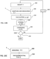
Figures 13A ,13B, 13C : show process steps of the present process. - In order to characterize the behavior of a power module, the thermal wave theory predicts that the thermal response of the surface of a homogeneous infinite material half-space subjected to a thermal excitation P 0 = P 0 (1 + cos(ω ))/2 is shifted by

figure 3 show the effect of a defect of strength R positioned a depth d on the phase shift of the surface temperature response as disclosed in document Rigert "Induktions-Lockin-Thermografie : ein neues Verfahren zur zerstörungsfreien Prüfung" http://dx.doi.org/10.18419/opus-1734. This chart shows the influence of the defect depth d (normalized with µ, a material parameter), and the reflection coefficient R (R=0=> no defect (perfect transmission); R=1=> strong defect (perfect reflection)). - It can be seen that when a defect is positioned at d<1.55 µm and has a coefficient of reflection R>0.4, the surface temperature response phase shift changes from the semi-infinite body value of 45° to a lower value that depends on R and on the position of the defect.
-
Figure 3 thus shows the basic principle of lock-in thermography to characterize defects and interfaces in materials, devices including a module stack-up. - Importantly the value of µ is frequency dependent: for defects located further into the material, greater sensitivity is obtained when lower excitation frequency is used. Thus, by varying the excitation frequency, information about interface (degradation) of different layer stack or interface can be gained.
- Although this simple model can give a good guidance on methods using thermal waves to detect damage, a power semiconductor stack cannot be modelled by a semi-infinite body, due to the different thermal properties of each layer of the stack. In order to analyze this system more precisely a 1D electrical equivalent of the thermal model can be used, one which the frequency response function can by analyzed.
- Thermal impedance: electrical equivalent model:
On the basis that heat conduction and electronic conduction are both physical processes modelled by the same phenomenon (diffusion), the thermal impedance of a semiconductor module can be modelled by analogy with the scaled heat conduction equation and the telegrapher's equations. Thus, an equivalent electrical network of the thermal system can be deduced. The resistances and capacitances of the electrical equivalent are defined by analogy with a thermal resistance, Rth and capacitance Cth, using the following equations:
- Where l is the thickness;
- A is the cross section area ;
- λ is the thermal conductivity,

- Where c is the specific heat capacity [J/g];
- V is the volume [m3];
- ρ is the density [g/m3].
- In the case of a simple model of power module composed with a stack-up of different materials, each layer will present a thermal resistance and a thermal capacitance. Thus, an electrical network, called Cauer network, can represent the thermal system of a stack-up of 5 layers as shown in Erreur ! Source du renvoi introuvable.. Ploss is the heat flux from the semiconductor die 5 of
figure 1 , corresponding to the losses dissipated on the semiconductor die (the electrical equivalent is a current source), Cth and Rth are the equivalent capacitance and resistance of each layer starting with thedie layer 3 and theheatsink layer 5 and Tamb is the environment heatsink temperature. - The total thermal impedance of the network of
figure 4 can be calculated using the following equation where s is the Laplacian operator:
- For the case of a degraded layer, a new (increased) resistance R th,v may be calculated using a percentage of void, f, as described in the next equation. As the material quantity is not modified, the thermal capacitance C h remains unchanged:

- For example, in the case of the stack-up of nine layers described in
figure 1 and the material data of Erreur I Source du renvoi introuvable. hereunder:Table 1: Stack up layers λ W/mK ρ g/cm3 c J/gK l mm 3 (silicon) 80 2,3 0, 7l2 0,l4 4 (die attach) 50 7,4 0,24 0, l 6 404 8,9 0,385 0,3 7 l60 3,3 0,72 0,7 9 450 8,9 0,385 0,32 l0 60 7,4 0,24 0,4 ll 450 8,9 0,385 4 l2 30 l,8l 0,85 0, l5 8 239 2,7 0,92l 20 - The thermal impedance may be plotted in a bode diagram, where the amplitude and the phase are plotted in function of the excitation frequency of a sinus type. In the curves of
Figures 5 to 7 a comparison is done between a pristine, that is non-degraded module, and a degraded module according tofigure 1 with measurements done at increasing frequencies. -
Figure 5 is the Bode diagram of a stack according tofigure 1 with thelayer 4 and thelayer 10 having 40% of voids.Figure 6 is the Bode diagram of a stack according tofigure 1 with thelayer 4 has 40% of voids.Figure 7 is the Bode diagram of a stack according tofigure 1 with thelayer 10 has 40% of voids. These figures show that the amplitude and the phase of the thermal impedance are modified by the degradation. -
Curves figure 5 , curves 36, 37 offigure 6 and curves 40, 41 offigure 7 are representing the phase difference between the temperature variations of the die for of pristine in dotted line and degraded layers in plain lines.Curves figure 5 , curves 34, 35 offigure 6 and curves 38, 39 offigure 7 are representing the amplitude of the temperature variation of the die with pristine in dotted line and degraded layers in plain lines. - the influence of a degradation of
layer 4 which is located close to the excitation source can best be detected by a phase shift ofcurve 33 with respect tocurve 32 at about 100Hz excitation as infigures 5 and 6 , whereas a relatively lower excitation frequency from about 1 to 10Hz is required to detect a frequency shift betweencurve 40 andcurve 41 corresponding to a damage inlayer 10 which is located further away from the heat source as seen infigure 7 . Note that no phase shift change is observed at 100Hz in case damage is introduced inlayer 10. Thus, by varying the excitation frequency, it is possible to gain information on which layer is damaged. - The previous section described the thermal response of the system to a sinusoidal excitation. In real application cases the power dissipation does not necessarily follow a sinusoidal behavior. The goal of this section is to describe the necessary conditions of the semiconductor operating point that generate a suitable thermal response of the system such that an information on a layer degradation can be gained. To support the loss profile requirements, the bode diagram of
figure 6 is plot on a larger frequency range as infigure 8 where the interval goes from 1Hz to 1 MHz.
In the present example,figure 8 shows the following information: - The magnitude of the bode diagram gives essentially the same information as a thermal impedance plot;
- The phase information shows that the
curves curves - Advantageously to the present invention, typical signal modulation strategies such as PWM modulation in converters typically operate at frequencies higher than 1kHz, such as 5kHz, or 10kHz. In consequence, the thermal system response will be weak in this frequency range, and the temperature oscillations due to the PWM frequency will be weak as seen in the magnitude of the bode plot <-60dB of
figure 8 . Thus, advantageously, the thermal system will not be influenced by the PWM excitation. For the use of the model described in the previous section this justifies that the losses can be averaged over a PWM period. - Advantageously to the present invention, typical excitation frequencies may be limited by the load impedance, by the load requirements, or by the external control of the system, such that the system is typically excited in the frequency range of interest, i.e., at a frequency lower than 1kHz, for example 50Hz, 60Hz, 100Hz, 400Hz, or 1 Hz.
- Another implication of this analysis is that a low frequency electrical excitation signal should not decrease from the maximum power value to the zero-power value within a time interval lower than τd .
- Thus, to summarize the power semiconductor losses requirements within the present invention: the power semiconductor die losses waveform is dependent on the application where the power module or system is installed.
- This invention relates to the cases of DC/AC or AC/DC power converter topologies, and to the cases where the losses are low frequency periodic pulsating waves with the following characteristics:
- a. A maximum pulse duration of a half-period of the fundamental frequency of the AC current, such that there exists a zero-loss time interval
- As an example, for condition c, the semiconductor chip is a silicon chip of thickness ld =100µm, the thermal diffusivity coefficient of silicon is Dd =4.89 10-4 m2/s, and thus fd = 4.89kHz, and τd =205µs.
- An example of DC/AC power topology is shown in
figure 9 where aDC supply 51 serves to build a three-phase alternating supply 52 using power semiconductor switches 1. The DC/AC power converter has a 3-phase configuration supplied by a DC bus voltage. The semiconductor die can be any IGBT, Diode, MOSFET, MISFET and in any placement of the power converter topology. In the following example, the semiconductor die of interest in the power module is placed in one leg at the high side position. - The switching and conduction losses of the semiconductor die 50 are generated in a normal operation of the power module in a motor control application given the load current, the bus voltage during the switching and conduction events.
- The semiconductor die losses generation in a power module on a DC/AC or DC/AC operation is proportional to the following variables that are related to the operating point: the current passing through Icond , the switched current Isw , the switched voltage Vsw , the switching frequency fsw , the junction temperature, Tj , the duty cycle modulation strategy / PWM technique.
- In such an application, typically, a periodic pulsed loss waveform in an DC/AC or AC/DC application is generated in the fundamental frequency, e.g., a grid frequency 50Hz or an electrical motor rotation control frequency of 1Hz - 2kHz. In any strategy, the losses on the semiconductor are generated only during a time corresponding to a first half-cycle of the fundamental frequency, and the semiconductor does not generate any losses during the second half cycle of the fundamental frequency.
- Considering that the power converter generates a sinusoidal current waveform, at the fundamental frequency of 100Hz, on the output of the phases ABC and a chopped voltage waveform at the switching frequency operation of 20kHz.
-
Figures 10A and10B are representation of the junction temperature and losses for a pristine and degraded power module at 100Hz of fundamental AC frequency.Figure 10A is a general view of the power and junction temperature waves with respect to time,Figure 10B is a zoomed figure on one loss period comprising also a measurement of the die temperature Tj duration time. In this example, the losses wave 70 infigure 10A on the semiconductor die has only the positive sinusoidal shape. In other words, the losses follow a sinusoidal shape between 0° and 180° (0 and π) and have a null value between 180° and 360° (π and 2 π) within the fundamental frequency ff :
- The temperature response Tj of the die 71, 72 in
figure 10A is calculated using the thermal impedance. The temperature wave has one minimum 71a, 72a and one maximum 71b, 72b within a fundamental period. When measuring the time between the minimum temperature point and the maximum temperature point gives an indicator of the module degradation. Infigure 10B showing a single loss period, it can be seen that the degraded power module with 40% of voids in layer 4offigure 1 operating at 100Hz of AC current has a longer duration time Δt=td than that of the pristine power module Δt=tp. This can be explained by the bode diagram offigure 6 , showing a larger absolute phase angle for the degraded thermal impedance compared to the pristine thermal impedance at 100Hz. - An important point is that it is possible only by examination of the temperature response to identify the beginning of the pulse corresponding to tTjmin, because the sudden power change generates a kink in the temperature response. Thus, advantageously, the information of Δt=tTjmax-tTjmin is related to the phase angle between the temperature response and the power excitation.
-
Figure 11 shows the losses in the fundamental frequency of the converter plotted for different modulation strategies when a DC/AC power converter drives an electrical motor. The different modulation strategies are:Sine 60,DPWM1 61,DPWM3 62,Spacevector 63. The losses are calculated considering both the conduction losses and the switching losses of the semiconductor die, and averaged over a modulation period. - The topologies of the converter are not limited to the converter taken as an example but could be multilevel topologies as the NPC (neutral point clamped inverter), ANPC (Active-neutral-point-clamped inverter), MMC (modular multilevel converter), FC (flying capacitor) and other topologies that are the state of art.
- This shows that in an AC/DC or DC/AC power converter having a power module comprising at least a semiconductor die attached to a material stack-up for the thermal dissipation and/or for electrical connections, where the semiconductor dissipates an asymmetrical loss between two half cycles of the AC frequency, measuring a signal related to the temperature of the semiconductor at said frequency, measuring the time duration Δt=tTjmax-tTjmin between the temperatures Tjmax and Tjmin where the junction temperature is at the maximum and respectively its minimum value, in an AC period permits to obtain a measurement of the degradation of at least one layer in a stack of layers between the die and a heatsink to which the die is attached by repeating such measurements during life of the power converter.
- Thus, advantageously since de degradation is sensitive to the temperature increase time delay Δt, and not to the magnitude of the temperature, nor the magnitude of the power losses the thermal degradation estimation is not sensitive to the accuracy of the junction temperature measurement, and thus any signal related to the temperature of the semiconductor can be used, provided there is a monotonous relation between the temperature and the signal. It is not necessary to estimate or measure the power losses in the semiconductor, thus advantageously reducing the number of sensors, the computation time and increasing the accuracy of the degradation measurement.
- In order to repeat measurements and compare such during the life of the converter, the calculations of the temperature increase time delay Δt= tTjmax- tTjmin may be stored in a memory at each iteration and compared with an initial value and/or a previous value and the evolution of such time delay Δtx for tx=t0 to tp may be monitored to obtain the degradation state of the thermal impedance.
- In addition to the measurement of the temperature increase time delay, the fundamental frequency ffund at which the losses are measured may be measured and stored and the degradation state is determined by the time duration Δt(ffund) at said fundamental frequency.
- Thus, advantageously, degradation information of a specific stack layer can be gained, as the variation of the damage indicator Δtx is sensitive to the fundamental frequency.
- For example, the fundamental loss frequency can be measured using the AC load current probe, or be given by the controller reference, or be given by the user AC frequency request.
- As discussed hereunder, damages at different height in the stack causes different phase shift in the temperature increase curves and measuring damage indicators Δti(ffund,i) at different frequencies ffund,i enables to gain information on the degradation evolution at different layers of the stack. The higher frequencies are used to monitor a degradation of the stack layers closer to the semiconductor and the lower frequencies are used to monitor a degradation of the stack layers farther from the semiconductor.
- The effect of the degradation on the frequency response functions for a specific layer of the stack can be determined by introducing a degradation in a specific layer, for
example using equation 4, measuring the phase shift associated with this degradation using the Z(s) estimation ofequation 3, and plotting a bode diagram as in figures 5 to 7. - As an example, one or several frequencies between 20Hz to 500Hz are used to monitor the degradation on the
layer 4 according to Figure 6 and one or several frequencies between 1Hz to 10Hz are used to monitor thelayer 10 resulting in the curve of figure 7. - In the case of a combination of several degradations, monitoring of the time delay at several frequencies enables to separate the contributions of the several degradations as in the example of figure 5.
- To support the relation between Δt and the phase angle, as a first approximation, the change of phase angle Ph in angular unit of degrees (°) due to the degradation, that is the change from Δt=tp to Δt=td can be approximated by the following equation:

- Figure 12 shows a comparison of first-order estimation of the phase Ph using equation (8), and the phase extracted from calculations using the impedance method with respect to the fundamental frequency. In this diagram,
curve 80 is the estimated phase curve fordegraded layers curve 81 is the theoretical curve for such degraded layers,curve 82 is the estimated phase curve fordegraded layer 4 whilecurve 83 is the theoretical curve fir such degraded layer,curve 84 is the estimated phase curve for degradelayer 10 andcurve 85 the theoretical curve for such degraded layer 10.This shows that for frequencies above around 10 Hz, the first order estimation shows similar trend as the more rigorous model, thus demonstrating that the information in Δt is the same as in the phase of the bode diagrams of figures 5 to 8. - Then, in case the fundamental frequency f of the AC current may be changed, the process may monitor the time difference for different fundamental frequencies. This gives a possibility to provide estimation of which of the layers are degraded layers.
- As the time difference Δtmin between two successive minima of the junction temperature is measured, the fundamental frequency may be calculated as ffund= 1/Δtmin
- Thus, advantageously, this allows to record the fundamental frequency without using an additional sensor, or without acquiring the fundamental frequency information from a separate algorithm. Thus, advantageously, the algorithm for degradation analysis can work independently of a control algorithm of the converter or any other operating condition of the power module.
- In example, in
figure 10A , the time interval between two successive minima is Δtmin =0.02s, and thus the fundamental frequency is found as ffund=1/Δtmin=50Hz. - The signal used for measuring the temperature may be any thermal sensitive electrical parameter (TSEP) of the concerned semiconductor switch.
- Thus, the deterioration can be identified and quantified without any complex prior TSEP calibration, reducing the complexity of the system.
- For example, the TSEP can have values X between Xa and Xb corresponding, for example to the range of temperature [-20C;200C], and the relation between the temperature and the TSEP is linear such as:
T=XA+B in [Xa;Xb] where A and B are constant - In this example, it is not necessary to calibrate the TSEP, i.e., to determine A and B before implementing the method since only the variable X is measured. In a sub example, A>0, and the moments tTjmax and tTjmin where the junction temperature is at the maximum correspond to the moments where X is at the maximum, respectively at the minimum value. In another sub example, A<0, and the moments tTjmax and tTjmin where the junction temperature is at the maximum correspond to the moments where X is at the minimum, respectively at the maximum value.
- More generally, it is sufficient that the function T(X) is monotonously increasing or decreasing, e.g., that its first derivative does not change sign in the interval [Xa;Xb]. Thus, advantageously non-calibrated TSEP with a non-linear temperature characteristic can also be used in the scope of the present disclosure.
- In
figure 13A are shown process steps of the present disclosure with the process comprising: - Step 100: sampling and measuring a signal S relating to the junction temperature Tj of said semiconductor die at a frequency higher than ten time said AC frequency of said AC current 100,
- Step 110 calculating a time duration Δt= tTjmax- tTjmin between a moment tTjmax, where said junction temperature of said semiconductor die is at a maximum value, and a moment tTjmin, where said junction temperature is at a minimum value, in one period of said AC current, and step 120 storing said time duration Δt in a memory,
- step 130 comparing said time durations Δtt0 to Δttp for t=t0 to tp values for monitoring an evolution of said time duration Δt to determine an evolution of degradation of the thermal impedance of said power module;
- repeating 140, 150 said sampling and measuring said signal and said calculating said time duration at different times tx=t0 to tp during the operating life of the power module to provide a series of time durations Δtt0 to Δttp.
- Step 100 may also comprise measuring said AC frequency and step 120 may comprise storing couple of time duration Δttx and AC frequency, ffund values.
- Measuring in
step 100 may be done with several means such as thermocouple, infrared image, TSEP etc. - Since there may be some noise in the measurements, averaging of the Δt values may be required and the comparison may not be done strictly with the first Δt0 value measured, but rather with a mean value over a measurement period of a few alternances at the beginning of the product usage. In such case, the averaging may be done on about two to ten alternances.
- Repetition of the sampling, measuring and the comparison maybe done on a regular basis that is every day, week, month or after a number of alternances of the AC frequency corresponding to the use of the converter (e.g., tenth or hundreds of hours) relevant with the estimated degradation rate. Repetition rate may also be accelerated when a difference between Δttx and Δt0 becomes larger than a predetermined warning value.
- The process may also comprise as shown in
figure 13B one ormore steps 260 of modifying said AC frequency during dedicated operation periods of said converter to provide several different AC frequencies fm= f1, f2, ..., fn each allowing to detect a thermal impedance of a specific layer of said stack up, repeating said sampling, and measuring the TSEP signal S and thefrequency 200 and said calculating 210 the time durations Δttxf1, Δttxf2, ... , Δttxfn corresponding to such different AC frequencies, - one or
more steps 230 of comparing said Δtt0fm to Δttpfm values at each of said AC frequencies for monitoring an evolution of Δt for each of said AC frequencies to determine an evolution of degradation of the thermal impedance of said specific layers, - repeating said sampling and measuring said signal and said calculating said time duration during the operating life of the power module to provide a series of Δtx= Δt0 to Δtp values for each of said different AC frequencies fm for comparing the Δtx values with the Δt0 value.
- Here also, repetition of the sampling, measuring and the comparison maybe done on a regular basis that is every day, week, month or after a number of alternances of the AC frequency corresponding to the use of the converter (e.g., tenth or hundreds of hours) relevant with the estimated degradation rate. Repetition rate may also be accelerated when a difference between Δttx and Δt0 becomes larger than a predetermined warning value.
- In addition, the tests using adaptation of the AC freqeuncy may be done in specific situations such as tests on the grid frequency or ramping of a motor speed.
- The process also may comprise as in
figure 13C one ormore steps 300 of measuring a time difference Δtmin between two successive minima of the junction temperature and calculating 310 said AC frequency as f=1/Δtmin. This avoids having to measure the frequency with another means than the signal S relating to the junction temperature Tj which may be a non-calibrated temperature sensitive electrical parameter of said semiconductor. - To proceed with the present process the converter as shown in
figure 9 may comprise sensor means 53 on a power semiconductor switch die of said converter for sensing a TSEP signal of said power semiconductor switch die, analog to digital converter means 54, sampling means 55 and aprocessor 56 provided with the necessary memory means 57 and computing means for storing and running a software configured for executing the thermal impedance monitoring process of the present disclosure.


Using the values of


The implication for the applicability of this invention is thus that the electrical excitation frequencies of interest should be significantly lower than

b. At least one local maximum inside the pulse, OR an asymmetrical loss dissipation between the two half-cycles.
AND
c. The time difference between the last maximum and the zero-loss time is larger than


Claims (14)
- - Thermal impedance monitoring process for a power module of a power converter used for transforming DC current to AC current, or vice-versa, where the semiconductor dissipates an asymmetrical loss between two half cycles of an AC frequency f of the AC current, said power module comprising at least a semiconductor die attached to a material stack-up of layers for its thermal dissipation and/or electrical connections, said process comprising:- sampling and measuring (100) a signal relating to the junction temperature Tj of said semiconductor die at a frequency higher than ten time said AC frequency of said AC current,- calculating (110) a time duration Δt= tTjmax- tTjmin between a moment tTjmax, where said junction temperature of said semiconductor die is at a maximum value, and a moment tTjmin, where said junction temperature is at a minimum value, in one period of said AC current, and storing (120) said time duration Δt in a memory,- repeating (140, 150) said sampling and measuring said signal and said calculating said time duration at different times tx=t0 to tp during the operating life of the power module to provide a series of time durations Δtt0 to Δttp , and comparing (130) said time durations Δttp values with Δtt0 for monitoring an evolution of said time duration Δtx to determine an evolution of degradation of the thermal impedance of said power module.
- - Thermal impedance monitoring process according to claim 1 comprising averaging the Δt measurements on periods for reducing noise in the measurements.
- - Thermal impedance monitoring process according to claim 1 or 2 comprising measuring said AC frequency( 200) and storing couple of time duration Δttx and AC frequency, ffund values (220).
- - Thermal impedance monitoring process according to claim 3 comprising modifying said AC frequency (260) during dedicated operation periods of said converter to provide several different AC frequencies fm=f1, f2, ..., fn each allowing to detect a thermal impedance of a specific layer of said stack up, repeating said sampling, and measuring and said calculating the time durations Δttxfm= Δttxf1, Δttxf2, ... , Δttxfn corresponding to such different AC frequencies,- repeating (240) said sampling and measuring said signal and said calculating said time duration during the operating life of the power module to provide a series of Δt0fm to Δtxfm values for each of said different AC frequencies, and comparing said Δttm values with Δtt0 at each of said AC frequencies for monitoring an evolution of Δt for each of said AC frequencies fm=f1, f2, ..., fn to determine an evolution of degradation of the thermal impedance of said specific layers.
- - Thermal impedance monitoring process according to claim 3 or 4 comprising measuring (300) a time difference Δtmin between two successive minima of the junction temperature and calculating said AC frequency as f=1/Δtmin.
- - Thermal impedance monitoring process according to any one of the preceding claims wherein the signal relating to the junction temperature Tj is a temperature sensitive electrical parameter of said semiconductor.
- - Thermal impedance monitoring process according to claim 6 wherein the signal relating to the junction temperature Tj is a non-calibrated temperature sensitive electrical parameter of said semiconductor.
- - Thermal impedance monitoring process according to any one of the preceding claims wherein said AC frequency is lower than

- - Thermal impedance monitoring process according to any one of the preceding claims wherein said AC frequency is lower than 2kHz.
- - Thermal impedance monitoring process according to any one of the preceding claims wherein said AC frequency is lower than 1kHz.
- - Thermal impedance monitoring process according to any one of the preceding claims wherein said AC frequency is the fundamental frequency powering the converter or the fundamental output frequency ffund of the converter.
- - Converter comprising sensor means (53) on a power semiconductor switch die of said converter for sensing a temperature of said power semiconductor switch die, analog to digital converter means (54), sampling means (55) and a processor (56) provided with memory means (57) for storing and running a software configured for executing the thermal impedance monitoring process according to any one of the preceding claims.
- - Converter according to claim 12 wherein said sensor means (53) are designed to sense a temperature sensitive electrical parameter of said power semiconductor switch die.
- - Permanent memory means comprising a software comprising instructions for executing the thermal impedance monitoring process according to any one of claim 1 to 11 when executed by a processor.
Priority Applications (4)
| Application Number | Priority Date | Filing Date | Title |
|---|---|---|---|
| EP22306944.4A EP4390349B1 (en) | 2022-12-19 | 2022-12-19 | Thermal impedance monitoring process for power modules |
| PCT/JP2023/029389 WO2024134969A1 (en) | 2022-12-19 | 2023-08-07 | Thermal impedance monitoring process for power module |
| CN202380086157.8A CN120500614A (en) | 2022-12-19 | 2023-08-07 | Thermal impedance monitoring process for power modules |
| JP2025539100A JP7851498B2 (en) | 2022-12-19 | 2023-08-07 | Method for monitoring the thermal impedance of power modules |
Applications Claiming Priority (1)
| Application Number | Priority Date | Filing Date | Title |
|---|---|---|---|
| EP22306944.4A EP4390349B1 (en) | 2022-12-19 | 2022-12-19 | Thermal impedance monitoring process for power modules |
Publications (2)
| Publication Number | Publication Date |
|---|---|
| EP4390349A1 true EP4390349A1 (en) | 2024-06-26 |
| EP4390349B1 EP4390349B1 (en) | 2025-10-29 |
Family
ID=84901345
Family Applications (1)
| Application Number | Title | Priority Date | Filing Date |
|---|---|---|---|
| EP22306944.4A Active EP4390349B1 (en) | 2022-12-19 | 2022-12-19 | Thermal impedance monitoring process for power modules |
Country Status (4)
| Country | Link |
|---|---|
| EP (1) | EP4390349B1 (en) |
| JP (1) | JP7851498B2 (en) |
| CN (1) | CN120500614A (en) |
| WO (1) | WO2024134969A1 (en) |
Citations (1)
| Publication number | Priority date | Publication date | Assignee | Title |
|---|---|---|---|---|
| US20220034958A1 (en) * | 2015-12-18 | 2022-02-03 | Zf Friedrichshafen Ag | Method and apparatus for detecting ageing of a power electronic apparatus comprising a semiconductor component, and power electronic system |
Family Cites Families (4)
| Publication number | Priority date | Publication date | Assignee | Title |
|---|---|---|---|---|
| JP3668708B2 (en) | 2001-10-22 | 2005-07-06 | 株式会社日立製作所 | Failure detection system |
| JP6861079B2 (en) | 2017-04-19 | 2021-04-21 | 株式会社日立製作所 | Power converter |
| JP7494041B2 (en) | 2020-07-29 | 2024-06-03 | 株式会社日立産機システム | Power conversion device and remote monitoring system |
| EP4099032B1 (en) | 2021-06-04 | 2023-12-20 | Mitsubishi Electric R & D Centre Europe B.V. | A method and a device for increasing the lifetime of power dies or power modules |
-
2022
- 2022-12-19 EP EP22306944.4A patent/EP4390349B1/en active Active
-
2023
- 2023-08-07 CN CN202380086157.8A patent/CN120500614A/en active Pending
- 2023-08-07 JP JP2025539100A patent/JP7851498B2/en active Active
- 2023-08-07 WO PCT/JP2023/029389 patent/WO2024134969A1/en not_active Ceased
Patent Citations (1)
| Publication number | Priority date | Publication date | Assignee | Title |
|---|---|---|---|---|
| US20220034958A1 (en) * | 2015-12-18 | 2022-02-03 | Zf Friedrichshafen Ag | Method and apparatus for detecting ageing of a power electronic apparatus comprising a semiconductor component, and power electronic system |
Non-Patent Citations (5)
| Title |
|---|
| BROECK: "In situ thermal impedance spectroscopy of Power electronic modules for localized degradation identification", PCIM EUROPE 2019; INTERNATIONAL EXHIBITION AND CONFERENCE FOR POWER ELECTRONICS, INTELLIGENT MOTION, RENEWABLE ENERGY AND ENERGY MANAGEMENT, 07-09 MAY 2019 NUREMBERG, GERMANY |
| GERD BUSSE: "Lockin-Thermography: Principles", NDE-APPLICATIONS AND TRENDS, JANUARY 2014 CONFERENCE: 2014 QUANTITATIVE INFRARED THERMOGRAPHY |
| POLOM: "2019 IEEE Applied Power Electronics Conference and Exposition (APEC", 17 March 2019, IEEE, article "Real-Time, In Situ Degradation Monitoring in Power Semiconductor Converters" |
| VAN DER BROECK CHRISTOPH H ET AL: "In-situ Thermal Impedance Spectroscopy of Power Electronic Modules for Localized Degradation Identification", PCIM EUROPE 2019, 7 May 2019 (2019-05-07), pages 1097 - 1104, XP093013165, Retrieved from the Internet <URL:https://ieeexplore.ieee.org/stampPDF/getPDF.jsp?tp=&arnumber=8767631&ref=aHR0cHM6Ly9pZWVleHBsb3JlLmllZWUub3JnL2RvY3VtZW50Lzg3Njc2MzE=> * |
| XIANG: "Condition Monitoring Power Module Solder Fatigue Using Inverter Harmonic Identification", IEEE TRANSACTIONS ON POWER ELECTRONICS, vol. 27, January 2012 (2012-01-01), pages 235 - 247, XP011389561, DOI: 10.1109/TPEL.2011.2160988 |
Also Published As
| Publication number | Publication date |
|---|---|
| JP2025530560A (en) | 2025-09-11 |
| EP4390349B1 (en) | 2025-10-29 |
| WO2024134969A1 (en) | 2024-06-27 |
| JP7851498B2 (en) | 2026-04-24 |
| CN120500614A (en) | 2025-08-15 |
Similar Documents
| Publication | Publication Date | Title |
|---|---|---|
| US11248966B2 (en) | Health monitoring and failure prognosis of power electronics devices | |
| Forest et al. | Use of opposition method in the test of high-power electronic converters | |
| JP5196370B2 (en) | Lifetime diagnosis device for power converter | |
| Wang et al. | Review of power semiconductor device reliability for power converters | |
| Hanif et al. | A comprehensive review toward the state-of-the-art in failure and lifetime predictions of power electronic devices | |
| Eleffendi et al. | In-service diagnostics for wire-bond lift-off and solder fatigue of power semiconductor packages | |
| Wang et al. | Real-time aging monitoring for IGBT modules using case temperature | |
| Choi et al. | Advanced accelerated power cycling test for reliability investigation of power device modules | |
| JP6899828B2 (en) | Methods and devices for detecting aging deterioration of power electronics equipment equipped with semiconductor components, and power electronics systems | |
| JP4367339B2 (en) | Electric motor control device | |
| Gao et al. | A temperature gradient-based potential defects identification method for IGBT module | |
| US7826985B2 (en) | Power module life estimation fatigue function | |
| EP1583197B1 (en) | Protection of power semiconductor components | |
| EP2682769B1 (en) | Apparatus for diagnosing DC link capacitor of inverter | |
| Arya et al. | Accurate online junction temperature estimation of IGBT using inflection point based updated I–V characteristics | |
| CN115616367B (en) | A method and system for online monitoring of power electronic device status information | |
| van der Broeck et al. | A test bench for thermal characterization of igbt power modules over mission profiles | |
| Wang et al. | SiC device junction temperature online monitoring | |
| Chen et al. | Driver Integrated Online R ds-on Monitoring Method for SiC Power Converters | |
| Halick et al. | Online computation of IGBT on-state resistance for off-shelf three-phase two-level power converter systems | |
| EP4390349B1 (en) | Thermal impedance monitoring process for power modules | |
| JP6714767B2 (en) | Power converter diagnostic circuit, power converter diagnostic system | |
| Entzminger et al. | Case temperature monitoring-based online condition monitoring of SiC MOSFET power modules using a radial basis function network | |
| Thurlbeck et al. | Machine learning based condition monitoring for sic mosfets in hydrokinetic turbine systems | |
| Pescetto et al. | Self-calibration technique for junction temperature estimation of SiC MOSFET inverters loaded with synchronous reluctance motors |
Legal Events
| Date | Code | Title | Description |
|---|---|---|---|
| PUAI | Public reference made under article 153(3) epc to a published international application that has entered the european phase |
Free format text: ORIGINAL CODE: 0009012 |
|
| STAA | Information on the status of an ep patent application or granted ep patent |
Free format text: STATUS: THE APPLICATION HAS BEEN PUBLISHED |
|
| AK | Designated contracting states |
Kind code of ref document: A1 Designated state(s): AL AT BE BG CH CY CZ DE DK EE ES FI FR GB GR HR HU IE IS IT LI LT LU LV MC ME MK MT NL NO PL PT RO RS SE SI SK SM TR |
|
| STAA | Information on the status of an ep patent application or granted ep patent |
Free format text: STATUS: REQUEST FOR EXAMINATION WAS MADE |
|
| 17P | Request for examination filed |
Effective date: 20241223 |
|
| GRAP | Despatch of communication of intention to grant a patent |
Free format text: ORIGINAL CODE: EPIDOSNIGR1 |
|
| STAA | Information on the status of an ep patent application or granted ep patent |
Free format text: STATUS: GRANT OF PATENT IS INTENDED |
|
| RIC1 | Information provided on ipc code assigned before grant |
Ipc: H02M 7/5387 20070101ALI20250331BHEP Ipc: H02M 1/32 20070101ALI20250331BHEP Ipc: G01K 7/42 20060101AFI20250331BHEP |
|
| INTG | Intention to grant announced |
Effective date: 20250411 |
|
| GRAJ | Information related to disapproval of communication of intention to grant by the applicant or resumption of examination proceedings by the epo deleted |
Free format text: ORIGINAL CODE: EPIDOSDIGR1 |
|
| STAA | Information on the status of an ep patent application or granted ep patent |
Free format text: STATUS: REQUEST FOR EXAMINATION WAS MADE |
|
| INTC | Intention to grant announced (deleted) | ||
| GRAP | Despatch of communication of intention to grant a patent |
Free format text: ORIGINAL CODE: EPIDOSNIGR1 |
|
| STAA | Information on the status of an ep patent application or granted ep patent |
Free format text: STATUS: GRANT OF PATENT IS INTENDED |
|
| INTG | Intention to grant announced |
Effective date: 20250703 |
|
| P01 | Opt-out of the competence of the unified patent court (upc) registered |
Free format text: CASE NUMBER: UPC_APP_0229_4390349/2025 Effective date: 20250711 |
|
| GRAS | Grant fee paid |
Free format text: ORIGINAL CODE: EPIDOSNIGR3 |
|
| GRAA | (expected) grant |
Free format text: ORIGINAL CODE: 0009210 |
|
| STAA | Information on the status of an ep patent application or granted ep patent |
Free format text: STATUS: THE PATENT HAS BEEN GRANTED |
|
| AK | Designated contracting states |
Kind code of ref document: B1 Designated state(s): AL AT BE BG CH CY CZ DE DK EE ES FI FR GB GR HR HU IE IS IT LI LT LU LV MC ME MK MT NL NO PL PT RO RS SE SI SK SM TR |
|
| REG | Reference to a national code |
Ref country code: CH Ref legal event code: F10 Free format text: ST27 STATUS EVENT CODE: U-0-0-F10-F00 (AS PROVIDED BY THE NATIONAL OFFICE) Effective date: 20251029 Ref country code: GB Ref legal event code: FG4D |
|
| REG | Reference to a national code |
Ref country code: IE Ref legal event code: FG4D |
|
| REG | Reference to a national code |
Ref country code: DE Ref legal event code: R096 Ref document number: 602022023897 Country of ref document: DE |
|
| PGFP | Annual fee paid to national office [announced via postgrant information from national office to epo] |
Ref country code: AT Payment date: 20260113 Year of fee payment: 4 |
|
| PGFP | Annual fee paid to national office [announced via postgrant information from national office to epo] |
Ref country code: FR Payment date: 20251121 Year of fee payment: 4 |
|
| REG | Reference to a national code |
Ref country code: NL Ref legal event code: MP Effective date: 20251029 |
|
| PG25 | Lapsed in a contracting state [announced via postgrant information from national office to epo] |
Ref country code: ES Free format text: LAPSE BECAUSE OF FAILURE TO SUBMIT A TRANSLATION OF THE DESCRIPTION OR TO PAY THE FEE WITHIN THE PRESCRIBED TIME-LIMIT Effective date: 20251029 |
|
| REG | Reference to a national code |
Ref country code: LT Ref legal event code: MG9D |
|
| PG25 | Lapsed in a contracting state [announced via postgrant information from national office to epo] |
Ref country code: NO Free format text: LAPSE BECAUSE OF FAILURE TO SUBMIT A TRANSLATION OF THE DESCRIPTION OR TO PAY THE FEE WITHIN THE PRESCRIBED TIME-LIMIT Effective date: 20260129 |
|
| PGFP | Annual fee paid to national office [announced via postgrant information from national office to epo] |
Ref country code: DE Payment date: 20251231 Year of fee payment: 4 |
|
| PG25 | Lapsed in a contracting state [announced via postgrant information from national office to epo] |
Ref country code: AT Free format text: LAPSE BECAUSE OF FAILURE TO SUBMIT A TRANSLATION OF THE DESCRIPTION OR TO PAY THE FEE WITHIN THE PRESCRIBED TIME-LIMIT Effective date: 20251029 Ref country code: FI Free format text: LAPSE BECAUSE OF FAILURE TO SUBMIT A TRANSLATION OF THE DESCRIPTION OR TO PAY THE FEE WITHIN THE PRESCRIBED TIME-LIMIT Effective date: 20251029 Ref country code: HR Free format text: LAPSE BECAUSE OF FAILURE TO SUBMIT A TRANSLATION OF THE DESCRIPTION OR TO PAY THE FEE WITHIN THE PRESCRIBED TIME-LIMIT Effective date: 20251029 |
|
| REG | Reference to a national code |
Ref country code: AT Ref legal event code: MK05 Ref document number: 1852031 Country of ref document: AT Kind code of ref document: T Effective date: 20251029 |
|
| PG25 | Lapsed in a contracting state [announced via postgrant information from national office to epo] |
Ref country code: NL Free format text: LAPSE BECAUSE OF FAILURE TO SUBMIT A TRANSLATION OF THE DESCRIPTION OR TO PAY THE FEE WITHIN THE PRESCRIBED TIME-LIMIT Effective date: 20251029 |
|
| PG25 | Lapsed in a contracting state [announced via postgrant information from national office to epo] |
Ref country code: RS Free format text: LAPSE BECAUSE OF FAILURE TO SUBMIT A TRANSLATION OF THE DESCRIPTION OR TO PAY THE FEE WITHIN THE PRESCRIBED TIME-LIMIT Effective date: 20260129 |
|
| PG25 | Lapsed in a contracting state [announced via postgrant information from national office to epo] |
Ref country code: IS Free format text: LAPSE BECAUSE OF FAILURE TO SUBMIT A TRANSLATION OF THE DESCRIPTION OR TO PAY THE FEE WITHIN THE PRESCRIBED TIME-LIMIT Effective date: 20260228 |
|
| PG25 | Lapsed in a contracting state [announced via postgrant information from national office to epo] |
Ref country code: PT Free format text: LAPSE BECAUSE OF FAILURE TO SUBMIT A TRANSLATION OF THE DESCRIPTION OR TO PAY THE FEE WITHIN THE PRESCRIBED TIME-LIMIT Effective date: 20260302 |
|
| PG25 | Lapsed in a contracting state [announced via postgrant information from national office to epo] |
Ref country code: PL Free format text: LAPSE BECAUSE OF FAILURE TO SUBMIT A TRANSLATION OF THE DESCRIPTION OR TO PAY THE FEE WITHIN THE PRESCRIBED TIME-LIMIT Effective date: 20251029 |
|
| PG25 | Lapsed in a contracting state [announced via postgrant information from national office to epo] |
Ref country code: LV Free format text: LAPSE BECAUSE OF FAILURE TO SUBMIT A TRANSLATION OF THE DESCRIPTION OR TO PAY THE FEE WITHIN THE PRESCRIBED TIME-LIMIT Effective date: 20251029 |
|
| PG25 | Lapsed in a contracting state [announced via postgrant information from national office to epo] |
Ref country code: BG Free format text: LAPSE BECAUSE OF FAILURE TO SUBMIT A TRANSLATION OF THE DESCRIPTION OR TO PAY THE FEE WITHIN THE PRESCRIBED TIME-LIMIT Effective date: 20251029 |