EP4387094A1 - Dc voltage regulation and tia with input-output dc voltage control - Google Patents
Dc voltage regulation and tia with input-output dc voltage control Download PDFInfo
- Publication number
- EP4387094A1 EP4387094A1 EP23211435.5A EP23211435A EP4387094A1 EP 4387094 A1 EP4387094 A1 EP 4387094A1 EP 23211435 A EP23211435 A EP 23211435A EP 4387094 A1 EP4387094 A1 EP 4387094A1
- Authority
- EP
- European Patent Office
- Prior art keywords
- tia
- voltage
- ldo
- output
- circuit
- Prior art date
- Legal status (The legal status is an assumption and is not a legal conclusion. Google has not performed a legal analysis and makes no representation as to the accuracy of the status listed.)
- Pending
Links
- 230000003287 optical effect Effects 0.000 claims abstract description 28
- 230000001427 coherent effect Effects 0.000 claims abstract description 13
- 238000000034 method Methods 0.000 claims description 16
- 235000004348 Perilla frutescens Nutrition 0.000 claims description 3
- 244000124853 Perilla frutescens Species 0.000 claims description 3
- 230000001105 regulatory effect Effects 0.000 description 24
- 238000010586 diagram Methods 0.000 description 13
- BKAYIFDRRZZKNF-VIFPVBQESA-N N-acetylcarnosine Chemical compound CC(=O)NCCC(=O)N[C@H](C(O)=O)CC1=CN=CN1 BKAYIFDRRZZKNF-VIFPVBQESA-N 0.000 description 6
- 230000008569 process Effects 0.000 description 6
- 239000003990 capacitor Substances 0.000 description 2
- 230000008859 change Effects 0.000 description 2
- 238000004891 communication Methods 0.000 description 2
- 230000003247 decreasing effect Effects 0.000 description 2
- 239000000203 mixture Substances 0.000 description 2
- 230000003071 parasitic effect Effects 0.000 description 2
- 230000004044 response Effects 0.000 description 2
- 239000008186 active pharmaceutical agent Substances 0.000 description 1
- 230000003321 amplification Effects 0.000 description 1
- 230000002238 attenuated effect Effects 0.000 description 1
- 230000008901 benefit Effects 0.000 description 1
- 230000001276 controlling effect Effects 0.000 description 1
- 238000007796 conventional method Methods 0.000 description 1
- 238000012937 correction Methods 0.000 description 1
- 230000008878 coupling Effects 0.000 description 1
- 238000010168 coupling process Methods 0.000 description 1
- 238000005859 coupling reaction Methods 0.000 description 1
- 230000007850 degeneration Effects 0.000 description 1
- 230000007613 environmental effect Effects 0.000 description 1
- 239000000835 fiber Substances 0.000 description 1
- 230000005669 field effect Effects 0.000 description 1
- 230000001939 inductive effect Effects 0.000 description 1
- 238000003199 nucleic acid amplification method Methods 0.000 description 1
- 230000010363 phase shift Effects 0.000 description 1
- 238000012545 processing Methods 0.000 description 1
- 230000001902 propagating effect Effects 0.000 description 1
- 230000002040 relaxant effect Effects 0.000 description 1
- 238000005316 response function Methods 0.000 description 1
- 239000004065 semiconductor Substances 0.000 description 1
- 238000012358 sourcing Methods 0.000 description 1
- 238000012546 transfer Methods 0.000 description 1
Images




Classifications
-
- H—ELECTRICITY
- H03—ELECTRONIC CIRCUITRY
- H03F—AMPLIFIERS
- H03F3/00—Amplifiers with only discharge tubes or only semiconductor devices as amplifying elements
- H03F3/45—Differential amplifiers
- H03F3/45071—Differential amplifiers with semiconductor devices only
- H03F3/45076—Differential amplifiers with semiconductor devices only characterised by the way of implementation of the active amplifying circuit in the differential amplifier
- H03F3/4508—Differential amplifiers with semiconductor devices only characterised by the way of implementation of the active amplifying circuit in the differential amplifier using bipolar transistors as the active amplifying circuit
- H03F3/45085—Long tailed pairs
- H03F3/45089—Non-folded cascode stages
-
- H—ELECTRICITY
- H03—ELECTRONIC CIRCUITRY
- H03F—AMPLIFIERS
- H03F3/00—Amplifiers with only discharge tubes or only semiconductor devices as amplifying elements
- H03F3/45—Differential amplifiers
- H03F3/45071—Differential amplifiers with semiconductor devices only
- H03F3/45076—Differential amplifiers with semiconductor devices only characterised by the way of implementation of the active amplifying circuit in the differential amplifier
- H03F3/45475—Differential amplifiers with semiconductor devices only characterised by the way of implementation of the active amplifying circuit in the differential amplifier using IC blocks as the active amplifying circuit
-
- G—PHYSICS
- G05—CONTROLLING; REGULATING
- G05F—SYSTEMS FOR REGULATING ELECTRIC OR MAGNETIC VARIABLES
- G05F1/00—Automatic systems in which deviations of an electric quantity from one or more predetermined values are detected at the output of the system and fed back to a device within the system to restore the detected quantity to its predetermined value or values, i.e. retroactive systems
- G05F1/10—Regulating voltage or current
- G05F1/46—Regulating voltage or current wherein the variable actually regulated by the final control device is DC
- G05F1/56—Regulating voltage or current wherein the variable actually regulated by the final control device is DC using semiconductor devices in series with the load as final control devices
-
- H—ELECTRICITY
- H03—ELECTRONIC CIRCUITRY
- H03F—AMPLIFIERS
- H03F1/00—Details of amplifiers with only discharge tubes, only semiconductor devices or only unspecified devices as amplifying elements
- H03F1/02—Modifications of amplifiers to raise the efficiency, e.g. gliding Class A stages, use of an auxiliary oscillation
- H03F1/0205—Modifications of amplifiers to raise the efficiency, e.g. gliding Class A stages, use of an auxiliary oscillation in transistor amplifiers
- H03F1/0211—Modifications of amplifiers to raise the efficiency, e.g. gliding Class A stages, use of an auxiliary oscillation in transistor amplifiers with control of the supply voltage or current
- H03F1/0216—Continuous control
- H03F1/0233—Continuous control by using a signal derived from the output signal, e.g. bootstrapping the voltage supply
-
- H—ELECTRICITY
- H03—ELECTRONIC CIRCUITRY
- H03F—AMPLIFIERS
- H03F3/00—Amplifiers with only discharge tubes or only semiconductor devices as amplifying elements
- H03F3/04—Amplifiers with only discharge tubes or only semiconductor devices as amplifying elements with semiconductor devices only
- H03F3/08—Amplifiers with only discharge tubes or only semiconductor devices as amplifying elements with semiconductor devices only controlled by light
- H03F3/087—Amplifiers with only discharge tubes or only semiconductor devices as amplifying elements with semiconductor devices only controlled by light with IC amplifier blocks
-
- H—ELECTRICITY
- H03—ELECTRONIC CIRCUITRY
- H03F—AMPLIFIERS
- H03F3/00—Amplifiers with only discharge tubes or only semiconductor devices as amplifying elements
- H03F3/04—Amplifiers with only discharge tubes or only semiconductor devices as amplifying elements with semiconductor devices only
- H03F3/14—Amplifiers with only discharge tubes or only semiconductor devices as amplifying elements with semiconductor devices only with amplifying devices having more than three electrodes or more than two PN junctions
-
- H—ELECTRICITY
- H03—ELECTRONIC CIRCUITRY
- H03F—AMPLIFIERS
- H03F3/00—Amplifiers with only discharge tubes or only semiconductor devices as amplifying elements
- H03F3/45—Differential amplifiers
- H03F3/45071—Differential amplifiers with semiconductor devices only
- H03F3/45479—Differential amplifiers with semiconductor devices only characterised by the way of common mode signal rejection
- H03F3/45484—Differential amplifiers with semiconductor devices only characterised by the way of common mode signal rejection in differential amplifiers with bipolar transistors as the active amplifying circuit
- H03F3/45488—Differential amplifiers with semiconductor devices only characterised by the way of common mode signal rejection in differential amplifiers with bipolar transistors as the active amplifying circuit by using feedback means
- H03F3/45493—Measuring at the loading circuit of the differential amplifier
- H03F3/45497—Controlling the input circuit of the differential amplifier
-
- H—ELECTRICITY
- H03—ELECTRONIC CIRCUITRY
- H03F—AMPLIFIERS
- H03F3/00—Amplifiers with only discharge tubes or only semiconductor devices as amplifying elements
- H03F3/45—Differential amplifiers
- H03F3/45071—Differential amplifiers with semiconductor devices only
- H03F3/45479—Differential amplifiers with semiconductor devices only characterised by the way of common mode signal rejection
- H03F3/45484—Differential amplifiers with semiconductor devices only characterised by the way of common mode signal rejection in differential amplifiers with bipolar transistors as the active amplifying circuit
- H03F3/45488—Differential amplifiers with semiconductor devices only characterised by the way of common mode signal rejection in differential amplifiers with bipolar transistors as the active amplifying circuit by using feedback means
- H03F3/45493—Measuring at the loading circuit of the differential amplifier
- H03F3/45511—Controlling the loading circuit of the differential amplifier
-
- G—PHYSICS
- G05—CONTROLLING; REGULATING
- G05F—SYSTEMS FOR REGULATING ELECTRIC OR MAGNETIC VARIABLES
- G05F1/00—Automatic systems in which deviations of an electric quantity from one or more predetermined values are detected at the output of the system and fed back to a device within the system to restore the detected quantity to its predetermined value or values, i.e. retroactive systems
- G05F1/10—Regulating voltage or current
- G05F1/46—Regulating voltage or current wherein the variable actually regulated by the final control device is DC
- G05F1/461—Regulating voltage or current wherein the variable actually regulated by the final control device is DC using an operational amplifier as final control device
-
- H—ELECTRICITY
- H03—ELECTRONIC CIRCUITRY
- H03F—AMPLIFIERS
- H03F2200/00—Indexing scheme relating to amplifiers
- H03F2200/129—Indexing scheme relating to amplifiers there being a feedback over the complete amplifier
-
- H—ELECTRICITY
- H03—ELECTRONIC CIRCUITRY
- H03F—AMPLIFIERS
- H03F2203/00—Indexing scheme relating to amplifiers with only discharge tubes or only semiconductor devices as amplifying elements covered by H03F3/00
- H03F2203/45—Indexing scheme relating to differential amplifiers
- H03F2203/45008—Indexing scheme relating to differential amplifiers the addition of two signals being made by a resistor addition circuit for producing the common mode signal
-
- H—ELECTRICITY
- H03—ELECTRONIC CIRCUITRY
- H03F—AMPLIFIERS
- H03F2203/00—Indexing scheme relating to amplifiers with only discharge tubes or only semiconductor devices as amplifying elements covered by H03F3/00
- H03F2203/45—Indexing scheme relating to differential amplifiers
- H03F2203/45418—Indexing scheme relating to differential amplifiers the CMCL comprising a resistor addition circuit
-
- H—ELECTRICITY
- H03—ELECTRONIC CIRCUITRY
- H03F—AMPLIFIERS
- H03F2203/00—Indexing scheme relating to amplifiers with only discharge tubes or only semiconductor devices as amplifying elements covered by H03F3/00
- H03F2203/45—Indexing scheme relating to differential amplifiers
- H03F2203/45528—Indexing scheme relating to differential amplifiers the FBC comprising one or more passive resistors and being coupled between the LC and the IC
-
- H—ELECTRICITY
- H03—ELECTRONIC CIRCUITRY
- H03F—AMPLIFIERS
- H03F2203/00—Indexing scheme relating to amplifiers with only discharge tubes or only semiconductor devices as amplifying elements covered by H03F3/00
- H03F2203/45—Indexing scheme relating to differential amplifiers
- H03F2203/45722—Indexing scheme relating to differential amplifiers the LC comprising one or more source followers, as post buffer or driver stages, in cascade in the LC
Definitions
- Various example embodiments relate to electrical circuits and methods for voltage regulators, trans-impedance amplifiers, and optical receivers using such voltage regulators and trans-impedance amplifiers.
- Trans-impedance amplifiers are used in high speed fiber optic communication systems.
- TIAs provide a link between the optical-to-electrical photodetectors (PDs), and the downstream electronics.
- a TIA converts a current coming from the PDs into a voltage, thus providing transimpedance gain (ZT).
- ZT transimpedance gain
- This voltage is typically fed to an ADC, and the resulting signal may be processed in the digital domain.
- the TIA is desirably linear and has a well-controlled gain, in the relevant operating range, so that the ADC receives a voltage that is a linear representation of the current from the PDs and has a magnitude that matches the dynamic range of the ADC.
- An example embodiment of the present disclosure provides an apparatus comprising a TIA and an LDO circuit for providing a supply voltage to the TIA.
- the LDO circuit is configured to adjust the supply voltage responsive to a DC voltage at an output of the TIA.
- the LDO circuit is configured to adjust the supply voltage to lessen variations of the DC voltage at an output of the TIA.
- the LDO circuit is configured to control a common-mode DC output voltage of the TIA.
- the LDO circuit may comprise an operational amplifier configured to adjust the supply voltage to change the DC voltage at an output of the TIA towards a reference voltage. Some embodiments may further comprise an input DC current cancellation circuit configured to adjust a DC input voltage of the TIA towards the reference voltage.
- the output of the TIA may be configured to provide a differential output signal, and the DC voltage at an output of the TIA may be a common-mode DC voltage at the output of the TIA.
- the DC input voltage of the TIA is a common-mode DC voltage at the input of the TIA.
- the LDO circuit may be configured to regulate less than 50% of a supply DC current of the TIA.
- the LDO circuit may be configured to regulate a first portion of a supply DC current of the TIA, with the apparatus further comprising a current mirror for adding a second portion of the supply DC current to the first portion at a supply voltage node of the TIA.
- the first portion is less than 50% of the supply DC current of the TIA.
- the apparatus further comprises a source of reference current coupled to an input of the current mirror.
- the coherent optical receiver may comprise an optical hybrid and photodiodes to receive light from corresponding outputs of the optical hybrid.
- the coherent optical receiver may comprise the TIA and the LDO circuit, with first and second of the photodiodes being connected to corresponding inputs of the TIA.
- the LDO circuit may be configured to provide a common-mode feedback from the output of the TIA to regulate the supply voltage.
- a second example embodiment disclosed herein provides an apparatus comprising: a voltage regulating circuit for providing a regulated voltage to a node of the circuit, wherein a load is connected to the node.
- the voltage regulating circuit comprises a low-dropout voltage regulator (LDO) connected to provide a first portion of a load current to the node, and a second circuit connected to provide a second portion of the load current to the node.
- LDO low-dropout voltage regulator
- the second portion is at least half of the load current.
- the second circuit may comprise a reference current source and a current mirror coupling the reference current source to the node.
- the current mirror is configured to output the second portion of the load current.
- the apparatus may further comprise a TIA having a supply voltage terminal connected to the node.
- the LDO may be configured to adjust the regulated voltage responsive to deviations of an output DC voltage of the TIA from a reference DC voltage.
- any of the above embodiments of the second example may comprise a coherent optical receiver including the TIA and the voltage regulating circuit.
- the LDO may be configured to provide a common-mode feedback from the output of the TIA to regulate the supply voltage.
- An aspect of the present disclosure provides a method comprising: providing a supply voltage to a trans-impedance amplifier (TIA) using a low drop-out (LDO) circuit; and configuring the LDO circuit to adjust the supply voltage responsive to a DC voltage at an output of the TIA.
- TIA trans-impedance amplifier
- LDO low drop-out
- Some embodiments of the method may comprise the LDO adjusting the supply voltage toward a reference voltage to lessen variations of the DC voltage at the output of the TIA.
- FIG. 1 illustrates a block diagram of an example coherent optical receiver 100 to which embodiments of the present disclosure may relate.
- An optical signal 101 received from an optical communication link (not shown) is mixed with local oscillator (LO) light 103 in an optical hybrid 115.
- LO local oscillator
- Different mixtures of the optical signal 101 and LO light 103 from four output ports of the optical hybrid 115 are transmitted to two photodiode (PD) pairs 120.
- PD photodiode
- Each PD pair 120 may be suitably biased at mid-point.
- the two PDs of a pair measure mixtures of the received optical signal light with LO light with different relative phase shifts.
- the signals from the two PDs of a pair are coupled to the differential inputs of a corresponding TIA 130.
- Differential outputs of the TIAs are provided to respective ADCs 140, which are, in turn, connected to a DSP 150 for signal processing and data demodulation.
- FIG. 2 A block diagram of a typical TIA circuit 200, which may be implemented e.g. as an Application-Specific Integrated Circuit (ASIC), is shown in FIG. 2 . It includes a front-end TIA (FE-TIA) 210, which converts PD current(s), e.g. I INp , I Inn from a PD pair 120, into a voltage signal, followed by a series of one or more Variable Gain Amplifiers (VGA) 220 to provide further voltage amplification, and an output driver 230.
- the output driver 230 is typically a transconductor, which drives an on-chip termination resistor 240 as well as being connected to the inputs of the ADC 140.
- the TIA circuit 200 may also include a peak detector 250 to measure the output swing, and an Automatic Gain Control (AGC) loop 260, which adjusts the TIA gain in order to keep the peak output swing at a desired value in the presence of slow variations of the swing of the currents I INp , I INn input to the TIA.
- AGC Automatic Gain Control
- the TIA input signal amplitude can vary suddenly by >10x (20dB) due to events in the optical network. Such events can substantially change the optical signal propagating to an optical receiver, at a rate much lower than the baud rate or symbol rate of the optical signal.
- the DC voltage bias of internal nodes of a FE-TIA should preferably be kept at a desired value, which should not vary significantly with PVT (process, voltage, and temperature) variations, and variations of the TIA gain and/or variations of the input DC and AC signals.
- PVT process, voltage, and temperature
- FIG. 3 schematically illustrates an example TIA circuit 300 including the FE-TIA 210 having a shunt-feedback topology.
- the transimpedance (ZT) of the FE-TIA 210 is typically varied by varying the value R F of feedback resistor(s) 314.
- the feedback resistor(s) 314 may be a circuit having tunable resistance and one or more elements.
- Each of the feedback resistor 314 typically includes a voltage-controlled MOS transistor (not shown in FIG. 3 ) operated in the triode regime.
- the current versus voltage (I-V) characteristic of resistors implemented with triode MOS transistors typically becomes highly nonlinear when the drain-source voltage drop (V DS ) is not suitably close to 0 volts. Therefore, it may be desirable that the two terminals of the variable resistor 314 are kept at approximately the same DC level, i.e. the voltage drop ⁇ V RF across the resistor(s) 314 should be substantially zero, or at least the voltage drop ⁇ V RF should preferably be small enough so that the MOS transistor in the feedback resistor 314 is in its substantially linear regime of operation.
- One aspect of the present disclosure relates to a closed-loop technique for reducing the voltage drop ⁇ V RF across the TIA feedback resistor 314.
- the FE-TIA such as the FE-TIA 300 that is illustrated in FIG. 3 and that is typically followed by a VGA in a TIA circuit, e.g. as illustrated in FIG. 2 , will be referred simply as the TIA.
- FIGs. 4 - 6 and 9 illustrate examples of such FE-TIAs ("TIAs") according to the present disclosure.
- the DC current entering the TIA 210 can reach values of a few milli-amperes (mA) and vary significantly over time.
- a closed-loop input DC current cancellation circuit such as e.g. the IDC CANC 320 shown in FIG. 3 , is typically employed to absorb this current so that the TIA's input DC bias is maintained approximately at a desired reference value.
- the IDC CANC 320 includes an operational amplifier 322 driving a voltage-controlled current source 324, e.g. a bipolar or FET transistor, connected in a negative feedback loop to reduce the difference between the TIA input DC voltage and a reference voltage V REF,CMIN .
- the input terminal of the feedback resistor(s) 314 is set to a controlled DC voltage approximately equal to the reference voltage V REF,CMIN .
- the reference voltage V REF,CMIN is generated e.g. from an approximately PVT-independent reference circuit, such as the well-known "bandgap reference" (not shown in FIG. 3 ).
- the TIA input DC voltage is well controlled and stable in the presence of voltage, supply and process variations.
- the DC voltage of the output terminal of the variable resistor (circuit) 314 is set by the voltage amplifier 310 of the TIA ("core amplifier 310", shown as a gain stage with a gain A 0 in FIG. 3 ).
- This DC voltage is a function of supply variations and process and temperature variations of resistors, bias currents, and of threshold voltages inside the core amplifier 310.
- the DC voltage drop ⁇ V RF across the feedback resistor 314 can vary significantly, thereby reducing the TIA's linearity.
- FIG. 4 shows an example diagram of a typical TIA circuit 400 with a low-dropout regulator (LDO) 440 connected to a supply voltage VCC to provide a regulated supply voltage VCC REG to a TIA 410 with shunt-feedback resistor(s) 414 having resistance R F .
- the LDO 440 operates to reduce supply noise and to improve accuracy of the amplifier supply voltage, and therefore of the output DC bias.
- the output DC bias of the TIA still may vary due to process and temperature variations of other amplifier components.
- the output DC common-mode voltage V CMOUT is given approximately by (VCC REG - I DC,AMP *R L - V be,Q5/Q6 ).
- I DC,AMP is the tail DC current of an input stage 420 of the TIA 410
- R L is the resistance of load resistors 422 of the input stage 420
- V be,Q5/Q6 is the base - emitter voltage of transistors Q 5 and Q 6 of an emitter follower 430 the TIA 410.
- the value of the output DC common-mode voltage V CMOUT is therefore a function of regulated supply VCC REG , DC current I DC,AMP and the load resistance R L (which vary with process and temperature), and is also a function of the base-emitter voltages V be,Q5/Q6 of the bipolar transistors Q 5 and Q 6 , which may have a strong temperature dependency.
- an example TIA circuit 500 of the present disclosure is shown in FIG. 5 .
- an LDO 540 includes an operational amplifier (OpAmp) 542 with two inputs and one output.
- the output of the LDO 540 connects to a gate of a FET 548 to control the regulated supply voltage VCC REG 555 to the TIA.
- One of the OpAmp's inputs is connected to sense the DC common-mode component of the output voltage of a TIA 410 instead of sensing the amplifier supply voltage VCC as in the TIA-LDO configuration ("TIA circuit 400") shown in FIG. 4 .
- the voltage-sensing input terminal 544 of the LDO 540 i.e.
- one of the input terminals of the OpAmp 542, is connected to a common-mode node 534 of a differential output 505 of the TIA 410.
- An output common-mode (DC) voltage V CMOUT is an average between voltages at the positive (512) and negative (511) output terminals of the TIA 410, and can be measured, e.g., at a node electrically connected to the positive and negative TIA outputs by resistors of a same value, e.g. node 534.
- the LDO 540 operates by comparing a common-mode output voltage V CMOUT of the TIA 410 against a voltage reference V REF,CMIN .
- the LDO 540 adjusts the regulated supply voltage VCC REG 555 to reduce the magnitude of the difference
- CMFB common-mode feedback loop
- FIG. 6 illustrates an embodiment 600 of the TIA circuit 500 of FIG. 5 (“TIA circuit 600") including input DC cancellation circuit(s) 620, labeled "I DC CANC", e.g., as described above with reference to IDC CANC 320 shown in FIG. 3 .
- I DC CANC input DC cancellation circuit(s) 620
- V REF,CMIN may be used to set both the amplifier input common-mode voltage V CMIN , e.g. using the IDC CANC circuit 620, i.e, circuit 320 shown in FIG. 3 , and the common-mode output voltage V CMOUT .
- the circuits of FIGs. 5 and 6 operate to keep both the TIA input and output DC bias at a same reference value using a closed-loop control. If the loop gain of the feedback circuit implemented with the LDO 540 is sufficiently large, the DC bias may be substantially independent of PVT and TIA ZT variations.
- FIGs. 5 and 6 adds little complexity and power overhead compared to the scheme shown in FIG. 4 .
- An LDO used in the example closed-loop circuits of FIGs. 5 and 6 should preferably be operable to set the VCC REG with sufficient precision, to provide significant current to supply an input stage 420 of the TIA 410 (typically 10mA or more), and to provide low-noise operation and high power-supply rejection ratio (PSRR) across the 3dB bandwidth (BW) of the TIA.
- PSRR power-supply rejection ratio
- BW 3dB bandwidth
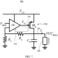
- a typical LDO 700 is based on a feedback loop, e.g. the feedback loop 710 from an output of an operational amplifier (OpAmp) 720 to one of the inputs thereof, via a transistor 730 "M 0 " and a resistor divider R 1 /R 2 .
- the OpAmp 720 controls the gate voltage of the transistor 730 to regulate a current I L output to a load 740 so as to make an output regulated voltage VCC REG at a regulated supply node 745 equal to a set function, e.g., a set fraction controlled by resistors R 1 and R 2 , of a stable reference V REF .
- the load 740 that connects to the regulated supply node 745 of the LDO 700 can be any circuit element sinking current from the load node 745, e.g. an amplifier or a TIA.
- the LDO operate stably in the presence of PVT variations and maintain a suitably high and wide-band power supply rejection ratio (PSRR), i.e., the transfer function between fluctuations of the unregulated supply voltage, e.g. Vcc in FIG. 7 , and fluctuations of the regulated output voltage, e.g. VCC REG in FIG. 7 .
- PSRR power supply rejection ratio
- a high PSRR may correspond to a Vcc noise attenuation of 20dB or more.
- the frequency response function of the feedback loop 710 of the LDO circuit 700 has two dominant poles (i.e. the lowest-frequency poles): one at node 755 "V G ", the gate of the transistor 730, the other at the regulated supply node 745 "VCC REG ".
- the frequency of the pole at node 755 "V G " is mostly impacted by a gate capacitance of transistor 730 "M 0 ", while the frequency of the pole at node 745 "VCC REG " is a function of capacitance C 0 .
- the pole at node 745 "VCC REG " should be set to be the lowest-frequency one. This may however require a very large value for capacitance C 0 (> 100pF). In discrete LDOs the capacitance C 0 is typically implemented off-chip, but for integrated LDOs C 0 should be an on-chip capacitor, resulting in significant chip area consumption.
- the second pole at node 755 "V G " is set to a frequency significantly higher than that of the dominant pole at node 745, so that the loop 710 does not become unstable.
- node 755 "V G " in the circuit of FIG. 7 is typically a highly capacitive load, since transistor 730 "M 0 " should be large enough to carry a load current of typically several mA while ensuring low-dropout operation.
- increasing the frequency of the second pole at node 755 is challenging, and may require either increasing the power consumption of the OpAmp 720, thus decreasing the LDO power efficiency, or increasing further the value of C 0 to move the dominant pole to lower frequency, thus further increasing the circuit area.
- FIG. 8 shows an example circuit diagram of a voltage regulating circuit 800 according to an embodiment of the present disclosure.
- the voltage regulating circuit 800 includes an LDO circuit 840, which may be as described above with reference to the LDO circuit 700 of FIG. 7 .
- the voltage regulating circuit 800 further includes a current mirror 820 connected at its output to the regulated supply node 845 and at its input to a current source 825 and configured to reduce the current through the transistor 730 "M 0 " of the LDO circuit 840.
- the current source 825 generates a partial replica current I REP,PART of an expected load current I Le , and a current mirror 820 formed with a transistor pair 821 "M 1 ", 822 “M 2 " generates a fixed output current I FIX , based on the partial replica current I REP,PART .
- the OpAmp 720 adjusts the current I LDO as needed to provide the desired value for the output voltage VCC REG at the regulated supply node 845, as set by the reference voltage V REF and the ratio of the resistances of resistors "R 1 " and “R 2 ".
- Sourcing a major portion, e.g. 50% or more, of the load current I L from a source external to the LDO feedback loop, e.g. the current mirror 820 providing a current I FIX proportional to a reference current I REP,PART , allows to significantly scale down the size of the transistor 730 "M 0 " compared to the LDO 700 of FIG. 7 .
- the parasitic capacitance at node 755 "V G " is reduced and the secondary pole of the LDO feedback loop 720 is pushed to a higher frequency, and the LDO stability issues are potentially mitigated.
- An expected, or nominal, value I Le of the load current I L for a particular TIA circuit may be estimated from the LDO circuit parameters and load, e.g.
- the replica current I FIX may be set to nominally provide from about 50% to about 90% of an expected load current I Le estimated for a given load 740, which allows reducing the current I LDO flowing through the transistor 730 "M 0 " proportionally by a factor of two or more.
- the replica current I FIX may be about 80% of the estimated load current I Le , which allows reducing the gate width of the transistor 730 "M 0 " to one fifth of the gate width without the replica current I FIX , since the LDO loop 710 only needs to provide about 20% of the load current I L .
- the parasitic capacitance at node 755 "V G " may be decreased by about a factor of about 5, which may be advantageous for LDO loop stability and for having a suitably high PSRR at high frequencies while relaxing requirements on the OpAmp power consumption and the C 0 footprint.
- a limited precision in generating the partial replica current I REP,PART may be compensated by the LDO feedback loop 720, which operates to adjust the I LDO by a corresponding amount so as to a maintain the regulated output supply voltage VCC REG at a target value set by the reference voltage V REF and, in the embodiments of FIG. 8 , by resistors "R 1 " and "R 2 ".
- the LDO feedback loop 720 may correct for variations in the partial current replica I REP,PART or for other circuit parameter variations by adjusting the current I LDO , as long as the current I LDO remains greater than zero Amperes (A) throughout the operation.
- the fixed current I FIX may therefore be chosen to ensure that the remaining portion of the load current I LDO remains non-zero over allowed variations of the circuit parameters and operation conditions.
- variations of the load current I L are expected to be within + ⁇ - 10% of a nominal value of the LDO current I LDO
- a nominal value of the fixed portion of the load current, i.e. I FIX may be about 80% of an expected value of the load current I L .
- the ratio of I FIX to I L may be adjusted up or down depending on the particular application and expected circuit and environmental parameter variations.
- the circuit topology illustrated in FIG. 8 may be suitable for an on-chip LDO providing voltage supply to an analog circuit such as, e.g., an amplifier or an oscillator.
- the load current I L is typically known and may not typically experience significant drifts over time.
- the partial replica current I REP,PART may be generated using conventional techniques for on-chip current generation.
- the regulated supply circuit 800 of FIG. 8 may have a precision in the output voltage control that is suitable for controlling the TIA output common-mode voltage V CMOUT in the circuit of FIGs. 5 or 6 . Accordingly, the LDO circuit of FIG. 8 may be used in place of the LDO 540 shown in FIGs. 5 or 6 .
- FIG. 9 illustrates an example TIA 900 using an embodiment of the LDO of FIG. 8 .
- a current source 905 provides a reference current I B to a current mirror 920 comprising transistors Q 7 and Q 8 .
- the current mirror 920 generates a current I EE ⁇ N * I B , N being a real number greater than 0, which biases an input stage 910 of the TIA 900.
- the input stage 910 is a differential cascode amplifier including transistor pairs (Q 1 /Q 2 ), (Q 3 /Q 4 ) and load resistors R L .
- Current mirrors 921 (transistors Q 7 and Q 11 ) and 922 (transistors Mi and M 2 ) are configured to source current I FIX ⁇ k*N*I B to regulated supply node 945 VCC REG .
- the current I FIX ⁇ k * I EE where the parameter k is set to e.g. 0.8 as discussed above.
- the remaining part, I LDO of the supply current I L is provided to the TIA by an LDO circuit 940 via transistor "M 0 ", which is driven by a feedback loop of the LDO circuit, that operates to set the TIA output common-mode voltage V CMOUT to a desired value, e.g. as described above with reference to FIG. 5 .
- the LDO circuit 940 includes an OpAmp 942 that operates to close the LDO feedback loop from an output of the OpAmp 942 to a TIA output common mode node 955, via the transistor M 0 , the TIA input stage 910, and the emitter follower stage 950 ( transistor pair "Q5", "Q6").
- the TIA circuit 900 in FIG. 9 may have about the same operation performance as the TIA circuit of FIG. 5 , but the amount of current provided by the transistor "M 0 " is substantially reduced, e.g., scaled down by a factor of (1- k ).
- the gate width of the transistor “M 0 " can also be correspondingly reduced, which is advantageous for the loop stability, PSRR, and power efficiency as discussed above. Since both of the currents I EE (i.e. the tail current of the TIA input stage 910) and I FIX (i.e. a "fixed" portion of the regulated supply current) in FIG. 9 are derived by mirroring bias current I B , the I FIX /I EE ratio may remain approximately constant if I B varies due to PVT variations.
- FIGs. 4 , 5 , 6 and 9 have a differential input to differential output configuration
- other embodiments may have single input to differential output configuration, single input to single output (SISO) configuration, or a differential input to single output configuration.
- SISO single input to single output
- the circuit in FIGs. 5 , 6 , and 9 may be modified so that LDO OpAmp senses the TIA single-ended output DC voltage, e.g.
- one of the LDO OpAmp inputs is connected to the TIA output node, or a passive or active low-pass filter is included wherein the filter input is connected to the TIA output node, and the filter output is connected to one of the LDO OpAmp inputs.
- any of the bipolar transistors shown in FIG. 4-9 may be implemented with a FET, and vice versa.
- the TIA core amplifier showed in FIG. 5 , 6 , and 9 may use a different topology than the differential cascode with the emitter follower output stage shown.
- the TIA might not include cascode transistors and/or might include a degeneration resistor and/or capacitor, and/or might include multiple output emitter followers, or no emitter folowers.
- the TIA might use one or more techniques to tune the amplifier gain such as current steering, variable tail current, variable impedance shunting or inductive peaking.
- a different circuit arrangement with respect to the one shown in FIG. 9 may be used to generate a partial replica of the TIA current I REP,PART , including but not limited to mixed-signal circuits using digital-to-analog converters and lookup tables.
- the OpAmp in FIG. 3-9 may be replaced with an Operational Transconductance Amplifier (OTA), i.e. an OpAmp with high output impedance, with no significant impact on the circuit operation.
- OTA Operational Transconductance Amplifier
- the LDO from FIG. 8 may provide a supply voltage to all or some of the TIA gain stages.
- the TIA may include additional low-frequency feedback loops, e.g. for offset correction.
Landscapes
- Engineering & Computer Science (AREA)
- Power Engineering (AREA)
- Physics & Mathematics (AREA)
- Electromagnetism (AREA)
- General Physics & Mathematics (AREA)
- Radar, Positioning & Navigation (AREA)
- Automation & Control Theory (AREA)
- Amplifiers (AREA)
Abstract
An apparatus, such as a coherent optical receiver, includes a trans-impedance amplifier, TIA, (410) and a low dropout, LDO, voltage regulator circuit for providing a supply voltage (VCC<sub>REG</sub>) to the TIA (410). The LDO circuit is configured to adjust the supply voltage responsive to a DC voltage (V<sub>CMOUT</sub>) at an output of the TIA (410). In some implementations the LDO circuit may provide only a fraction of a supply current to the TIA (410), with another fraction provided by a partial current replica source.
Description
- Various example embodiments relate to electrical circuits and methods for voltage regulators, trans-impedance amplifiers, and optical receivers using such voltage regulators and trans-impedance amplifiers.
- Trans-impedance amplifiers (TIAs) are used in high speed fiber optic communication systems. TIAs provide a link between the optical-to-electrical photodetectors (PDs), and the downstream electronics. A TIA converts a current coming from the PDs into a voltage, thus providing transimpedance gain (ZT). This voltage is typically fed to an ADC, and the resulting signal may be processed in the digital domain. The TIA is desirably linear and has a well-controlled gain, in the relevant operating range, so that the ADC receives a voltage that is a linear representation of the current from the PDs and has a magnitude that matches the dynamic range of the ADC.
- An example embodiment of the present disclosure provides an apparatus comprising a TIA and an LDO circuit for providing a supply voltage to the TIA. The LDO circuit is configured to adjust the supply voltage responsive to a DC voltage at an output of the TIA.
- In some embodiments of the above apparatus, the LDO circuit is configured to adjust the supply voltage to lessen variations of the DC voltage at an output of the TIA.
- In some embodiments of the above apparatus, the LDO circuit is configured to control a common-mode DC output voltage of the TIA.
- In any of the above embodiments, the LDO circuit may comprise an operational amplifier configured to adjust the supply voltage to change the DC voltage at an output of the TIA towards a reference voltage. Some embodiments may further comprise an input DC current cancellation circuit configured to adjust a DC input voltage of the TIA towards the reference voltage. In some of such above embodiments, the output of the TIA may be configured to provide a differential output signal, and the DC voltage at an output of the TIA may be a common-mode DC voltage at the output of the TIA. In some of such embodiments, the DC input voltage of the TIA is a common-mode DC voltage at the input of the TIA.
- In any of the above embodiments, the LDO circuit may be configured to regulate less than 50% of a supply DC current of the TIA.
- In any of the above embodiments, the LDO circuit may be configured to regulate a first portion of a supply DC current of the TIA, with the apparatus further comprising a current mirror for adding a second portion of the supply DC current to the first portion at a supply voltage node of the TIA. In some embodiments the first portion is less than 50% of the supply DC current of the TIA. In some embodiments, the apparatus further comprises a source of reference current coupled to an input of the current mirror.
- Some of the above embodiments may include a coherent optical receiver. The coherent optical receiver may comprise an optical hybrid and photodiodes to receive light from corresponding outputs of the optical hybrid. The coherent optical receiver may comprise the TIA and the LDO circuit, with first and second of the photodiodes being connected to corresponding inputs of the TIA. In any of the above embodiments, the LDO circuit may be configured to provide a common-mode feedback from the output of the TIA to regulate the supply voltage.
- A second example embodiment disclosed herein provides an apparatus comprising: a voltage regulating circuit for providing a regulated voltage to a node of the circuit, wherein a load is connected to the node. The voltage regulating circuit comprises a low-dropout voltage regulator (LDO) connected to provide a first portion of a load current to the node, and a second circuit connected to provide a second portion of the load current to the node. In some embodiments of the apparatus of the second example, the second portion is at least half of the load current.
- In any of the above embodiments of the second example, the second circuit may comprise a reference current source and a current mirror coupling the reference current source to the node. The current mirror is configured to output the second portion of the load current. In any of the above embodiments of the second example, the apparatus may further comprise a TIA having a supply voltage terminal connected to the node. In any of the above embodiments of the second example, the LDO may be configured to adjust the regulated voltage responsive to deviations of an output DC voltage of the TIA from a reference DC voltage.
- Any of the above embodiments of the second example may comprise a coherent optical receiver including the TIA and the voltage regulating circuit. The LDO may be configured to provide a common-mode feedback from the output of the TIA to regulate the supply voltage.
- An aspect of the present disclosure provides a method comprising: providing a supply voltage to a trans-impedance amplifier (TIA) using a low drop-out (LDO) circuit; and configuring the LDO circuit to adjust the supply voltage responsive to a DC voltage at an output of the TIA.
- Some embodiments of the method may comprise the LDO adjusting the supply voltage toward a reference voltage to lessen variations of the DC voltage at the output of the TIA.
- Embodiments disclosed herein will be described in greater detail with reference to the accompanying drawings which represent preferred embodiments thereof, in which like elements are indicated with like reference numerals, and wherein:
-
FIG. 1 is a schematic block diagram of a coherent optical receiver using the TIA(s) of the present disclosure may be used; -
FIG. 2 is a schematic block diagram of a TIA circuit that may be used in the coherent optical receiver ofFIG. 1 ; -
FIG. 3 is a circuit diagram of a shunt-feedback front-end TIA with a closed-loop input DC bias circuit; -
FIG. 4 is a circuit diagram of an example front-end TIA with an LDO; -
FIG. 5 is a circuit diagram of a front-end TIA with an LDO bias according to an embodiment of the present disclosure; -
FIG. 6 is a circuit diagram of an embodiment of the front-end TIA ofFIG. 5 with an input DC voltage cancellation using an LDO-shared voltage reference; -
FIG. 7 is a circuit diagram of a typical LDO; -
FIG. 8 is a circuit diagram of an LDO circuit according to an embodiment of the present disclosure. -
FIG. 9 is a circuit diagram of a front-end TIA powered by an embodiment of the LDO circuit ofFIG. 8 . - In the following description, for purposes of explanation and not limitation, specific details are set forth, such as particular circuits, circuit components, techniques, etc. in order to provide a thorough understanding of the present invention. However, it will be apparent to one skilled in the art that the present invention may be practiced in other embodiments that depart from these specific details. In other instances, detailed descriptions of well-known methods, devices, and circuits may be omitted so as not to obscure the description of the present invention. All statements herein reciting principles, aspects, and embodiments of the invention, as well as specific examples thereof, are intended to encompass both structural and functional equivalents thereof. Additionally, it is intended that such equivalents include both currently known equivalents as well as equivalents developed in the future.
- Furthermore, the following abbreviations and acronyms may be used in the present document:
- ADC: Analog to Digital Converter
- AGC: Automatic Gain Control
- AV: voltage gain
- BW: Bandwidth
- CMFB: Common Mode FeedBack
- DSP: Digital Signal Processor
- FET: Field-Effect Transistor
- LDO: Low DropOut regulator
- LNA: Low Noise Amplifier
- MOS: Metal-Oxide-Semiconductor
- OpAmp: Operational Amplifier
- PSRR: Power Supply Rejection Ratio
- PVT: Process/supply Voltage/Temperature
- SNR: Signal to Noise Ratio
- TIA: TransImpedance Amplifier
- ZT: transimpedance
- VDS: drain-source voltage drop
-
FIG. 1 illustrates a block diagram of an example coherentoptical receiver 100 to which embodiments of the present disclosure may relate. Anoptical signal 101 received from an optical communication link (not shown) is mixed with local oscillator (LO) light 103 in anoptical hybrid 115. Different mixtures of theoptical signal 101 and LO light 103 from four output ports of theoptical hybrid 115 are transmitted to two photodiode (PD) pairs 120. EachPD pair 120 may be suitably biased at mid-point. The two PDs of a pair measure mixtures of the received optical signal light with LO light with different relative phase shifts. The signals from the two PDs of a pair are coupled to the differential inputs of acorresponding TIA 130. Differential outputs of the TIAs are provided torespective ADCs 140, which are, in turn, connected to aDSP 150 for signal processing and data demodulation. - A block diagram of a
typical TIA circuit 200, which may be implemented e.g. as an Application-Specific Integrated Circuit (ASIC), is shown inFIG. 2 . It includes a front-end TIA (FE-TIA) 210, which converts PD current(s), e.g. I INp, I Inn from aPD pair 120, into a voltage signal, followed by a series of one or more Variable Gain Amplifiers (VGA) 220 to provide further voltage amplification, and anoutput driver 230. Theoutput driver 230 is typically a transconductor, which drives an on-chip termination resistor 240 as well as being connected to the inputs of theADC 140. TheTIA circuit 200 may also include apeak detector 250 to measure the output swing, and an Automatic Gain Control (AGC)loop 260, which adjusts the TIA gain in order to keep the peak output swing at a desired value in the presence of slow variations of the swing of the currents I INp, I INn input to the TIA. - For the coherent optical receiver illustrated in
FIG. 1 , the TIA input signal amplitude can vary suddenly by >10x (20dB) due to events in the optical network. Such events can substantially change the optical signal propagating to an optical receiver, at a rate much lower than the baud rate or symbol rate of the optical signal. In response to such events, gain of the TIA circuit may be adjusted by theAGC 260, so that the amplitude of the output signal, e.g. a differential output voltage ΔV OUT = (V OUTp-V OUTn), remains about constant and remains within a desirable operating range of theADC 140 connected to receive the output signals of theTIA circuit 200. - The DC voltage bias of internal nodes of a FE-TIA should preferably be kept at a desired value, which should not vary significantly with PVT (process, voltage, and temperature) variations, and variations of the TIA gain and/or variations of the input DC and AC signals.
-
FIG. 3 schematically illustrates anexample TIA circuit 300 including the FE-TIA 210 having a shunt-feedback topology. In this topology, which is typically used, e.g., for high-speed, low-noise applications, the transimpedance (ZT) of the FE-TIA 210 is typically varied by varying the value RF of feedback resistor(s) 314. The feedback resistor(s) 314 may be a circuit having tunable resistance and one or more elements. Each of thefeedback resistor 314 typically includes a voltage-controlled MOS transistor (not shown inFIG. 3 ) operated in the triode regime. One challenge is that the current versus voltage (I-V) characteristic of resistors implemented with triode MOS transistors typically becomes highly nonlinear when the drain-source voltage drop (VDS) is not suitably close to 0 volts. Therefore, it may be desirable that the two terminals of thevariable resistor 314 are kept at approximately the same DC level, i.e. the voltage drop ΔVRF across the resistor(s) 314 should be substantially zero, or at least the voltage drop ΔVRF should preferably be small enough so that the MOS transistor in thefeedback resistor 314 is in its substantially linear regime of operation. - One aspect of the present disclosure relates to a closed-loop technique for reducing the voltage drop ΔVRF across the
TIA feedback resistor 314. In the following, the FE-TIA, such as the FE-TIA 300 that is illustrated inFIG. 3 and that is typically followed by a VGA in a TIA circuit, e.g. as illustrated inFIG. 2 , will be referred simply as the TIA.FIGs. 4 - 6 and9 illustrate examples of such FE-TIAs ("TIAs") according to the present disclosure. - In coherent optical applications, the DC current entering the
TIA 210 can reach values of a few milli-amperes (mA) and vary significantly over time. A closed-loop input DC current cancellation circuit (IDC CANC), such as e.g. theIDC CANC 320 shown inFIG. 3 , is typically employed to absorb this current so that the TIA's input DC bias is maintained approximately at a desired reference value. TheIDC CANC 320 includes anoperational amplifier 322 driving a voltage-controlledcurrent source 324, e.g. a bipolar or FET transistor, connected in a negative feedback loop to reduce the difference between the TIA input DC voltage and a reference voltage VREF,CMIN. Due to this circuit, the input terminal of the feedback resistor(s) 314 is set to a controlled DC voltage approximately equal to the reference voltage VREF,CMIN. The reference voltage VREF,CMIN is generated e.g. from an approximately PVT-independent reference circuit, such as the well-known "bandgap reference" (not shown inFIG. 3 ). As a result, the TIA input DC voltage is well controlled and stable in the presence of voltage, supply and process variations. - On the other hand, the DC voltage of the output terminal of the variable resistor (circuit) 314 is set by the
voltage amplifier 310 of the TIA ("core amplifier 310", shown as a gain stage with a gain A0 inFIG. 3 ). This DC voltage is a function of supply variations and process and temperature variations of resistors, bias currents, and of threshold voltages inside thecore amplifier 310. As a result, the DC voltage drop ΔVRF across thefeedback resistor 314 can vary significantly, thereby reducing the TIA's linearity. -
FIG. 4 shows an example diagram of atypical TIA circuit 400 with a low-dropout regulator (LDO) 440 connected to a supply voltage VCC to provide a regulated supply voltage VCCREG to aTIA 410 with shunt-feedback resistor(s) 414 having resistance RF. TheLDO 440 operates to reduce supply noise and to improve accuracy of the amplifier supply voltage, and therefore of the output DC bias. However, the output DC bias of the TIA still may vary due to process and temperature variations of other amplifier components. - For example, in the
TIA circuit 400 ofFIG. 4 , the output DC common-mode voltage VCMOUT is given approximately by (VCCREG - IDC,AMP*RL - Vbe,Q5/Q6). Here IDC,AMP is the tail DC current of aninput stage 420 of theTIA 410, RL is the resistance ofload resistors 422 of theinput stage 420, Vbe,Q5/Q6 is the base - emitter voltage of transistors Q5 and Q6 of anemitter follower 430 theTIA 410. The value of the output DC common-mode voltage VCMOUT is therefore a function of regulated supply VCCREG, DC current IDC,AMP and the load resistance RL (which vary with process and temperature), and is also a function of the base-emitter voltages Vbe,Q5/Q6 of the bipolar transistors Q5 and Q6, which may have a strong temperature dependency. - An
example TIA circuit 500 of the present disclosure is shown inFIG. 5 . In the illustrated circuit, anLDO 540 includes an operational amplifier (OpAmp) 542 with two inputs and one output. The output of theLDO 540 connects to a gate of aFET 548 to control the regulatedsupply voltage VCC REG 555 to the TIA. One of the OpAmp's inputs is connected to sense the DC common-mode component of the output voltage of aTIA 410 instead of sensing the amplifier supply voltage VCC as in the TIA-LDO configuration ("TIA circuit 400") shown inFIG. 4 . In theTIA circuit 500 ofFIG. 5 , the voltage-sensing input terminal 544 of theLDO 540, i.e. one of the input terminals of theOpAmp 542, is connected to a common-mode node 534 of adifferential output 505 of theTIA 410. An output common-mode (DC) voltage VCMOUT is an average between voltages at the positive (512) and negative (511) output terminals of theTIA 410, and can be measured, e.g., at a node electrically connected to the positive and negative TIA outputs by resistors of a same value,e.g. node 534. In this embodiment, theLDO 540 operates by comparing a common-mode output voltage VCMOUT of theTIA 410 against a voltage reference VREF,CMIN. TheLDO 540 adjusts the regulatedsupply voltage VCC REG 555 to reduce the magnitude of the difference |VCMOUT- VREF,CMIN|. Therefore, theLDO 540 acts as a common-mode feedback loop (CMFB) for theTIA 410. -
FIG. 6 illustrates anembodiment 600 of theTIA circuit 500 ofFIG. 5 ("TIA circuit 600") including input DC cancellation circuit(s) 620, labeled "IDC CANC", e.g., as described above with reference toIDC CANC 320 shown inFIG. 3 . In some embodiments the same voltage reference VREF,CMIN may be used to set both the amplifier input common-mode voltage VCMIN, e.g. using theIDC CANC circuit 620, i.e,circuit 320 shown inFIG. 3 , and the common-mode output voltage VCMOUT. Since the inputs and outputs of acore amplifier 610 of theTIA 600 are connected to the two terminals of thefeedback resistors 314, setting the input and output common-mode of theTIA 600 to approximately the same voltage may have the advantage of reducing the DC voltage drop across thefeedback resistors 314 and may thereby improve the linearity of thevariable feedback resistors 314. - The circuits of
FIGs. 5 and6 operate to keep both the TIA input and output DC bias at a same reference value using a closed-loop control. If the loop gain of the feedback circuit implemented with theLDO 540 is sufficiently large, the DC bias may be substantially independent of PVT and TIA ZT variations. - Since typical TIAs incorporate an LDO to provide low-noise supply to the amplifier, the technique illustrated in
FIGs. 5 and6 adds little complexity and power overhead compared to the scheme shown inFIG. 4 . - An LDO used in the example closed-loop circuits of
FIGs. 5 and6 , such as e.g. theLDO 540, should preferably be operable to set the VCCREG with sufficient precision, to provide significant current to supply aninput stage 420 of the TIA 410 (typically 10mA or more), and to provide low-noise operation and high power-supply rejection ratio (PSRR) across the 3dB bandwidth (BW) of the TIA. Below an example LDO circuit is described that may be capable of meeting at least some of these expectations. - Referring to
FIG. 7 , atypical LDO 700 is based on a feedback loop, e.g. thefeedback loop 710 from an output of an operational amplifier (OpAmp) 720 to one of the inputs thereof, via atransistor 730 "M0" and a resistor divider R1/R2. TheOpAmp 720 controls the gate voltage of thetransistor 730 to regulate a current IL output to aload 740 so as to make an output regulated voltage VCCREG at aregulated supply node 745 equal to a set function, e.g., a set fraction controlled by resistors R 1 and R 2, of a stable reference VREF. Theload 740 that connects to theregulated supply node 745 of theLDO 700 can be any circuit element sinking current from theload node 745, e.g. an amplifier or a TIA. - It is typically desired that the LDO operate stably in the presence of PVT variations and maintain a suitably high and wide-band power supply rejection ratio (PSRR), i.e., the transfer function between fluctuations of the unregulated supply voltage, e.g. Vcc in
FIG. 7 , and fluctuations of the regulated output voltage, e.g. VCCREG inFIG. 7 . The greater is the PSRR, the stronger any fluctuations of the Vcc within the LDO bandwidth are attenuated in the VCCREG. For example, a high PSRR may correspond to a Vcc noise attenuation of 20dB or more. - Properties of an LDO circuit related to PSRR performance may be analyzed from the poles of a loop gain frequency response of the LDO circuit. The frequency response function of the
feedback loop 710 of theLDO circuit 700 has two dominant poles (i.e. the lowest-frequency poles): one atnode 755 "VG", the gate of thetransistor 730, the other at theregulated supply node 745 "VCCREG". The frequency of the pole atnode 755 "VG" is mostly impacted by a gate capacitance oftransistor 730 "M0", while the frequency of the pole atnode 745 "VCCREG" is a function of capacitance C0. To provide a wideband PSRR, as typically desired, the pole atnode 745 "VCCREG" should be set to be the lowest-frequency one. This may however require a very large value for capacitance C0 (> 100pF). In discrete LDOs the capacitance C0 is typically implemented off-chip, but for integrated LDOs C0 should be an on-chip capacitor, resulting in significant chip area consumption. - It may be further desired that the second pole at
node 755 "VG" is set to a frequency significantly higher than that of the dominant pole atnode 745, so that theloop 710 does not become unstable. However,node 755 "VG" in the circuit ofFIG. 7 is typically a highly capacitive load, sincetransistor 730 "M0" should be large enough to carry a load current of typically several mA while ensuring low-dropout operation. As a result, increasing the frequency of the second pole atnode 755 is challenging, and may require either increasing the power consumption of theOpAmp 720, thus decreasing the LDO power efficiency, or increasing further the value of C0 to move the dominant pole to lower frequency, thus further increasing the circuit area. -
FIG. 8 shows an example circuit diagram of avoltage regulating circuit 800 according to an embodiment of the present disclosure. Thevoltage regulating circuit 800 includes anLDO circuit 840, which may be as described above with reference to theLDO circuit 700 ofFIG. 7 . Thevoltage regulating circuit 800 further includes acurrent mirror 820 connected at its output to theregulated supply node 845 and at its input to acurrent source 825 and configured to reduce the current through thetransistor 730 "M0" of theLDO circuit 840. Thecurrent source 825 generates a partial replica current IREP,PART of an expected load current ILe, and acurrent mirror 820 formed with atransistor pair 821 "M1", 822 "M2" generates a fixed output current IFIX , based on the partial replica current IREP,PART. The fixed output current IFIX, which may be somewhat smaller than the expected load current I L, flows into a regulated supply node 845 ("load node") to which theload 740 is attached. Only the remaining part of the load current IL, i.e. the current ILDO = (IL - IFIX), is provided to said node by theLDO feedback loop 720 through thetransistor 730 "M0". TheOpAmp 720 adjusts the current ILDO as needed to provide the desired value for the output voltage VCCREG at theregulated supply node 845, as set by the reference voltage VREF and the ratio of the resistances of resistors "R1" and "R2". - Sourcing a major portion, e.g. 50% or more, of the load current IL from a source external to the LDO feedback loop, e.g. the
current mirror 820 providing a current IFIX proportional to a reference current IREP,PART, allows to significantly scale down the size of thetransistor 730 "M0" compared to theLDO 700 ofFIG. 7 . As a result, the parasitic capacitance atnode 755 "VG" is reduced and the secondary pole of theLDO feedback loop 720 is pushed to a higher frequency, and the LDO stability issues are potentially mitigated. An expected, or nominal, value ILe of the load current IL for a particular TIA circuit may be estimated from the LDO circuit parameters and load, e.g. TIA, specifications. In an example embodiment, the replica current IFIX may be set to nominally provide from about 50% to about 90% of an expected load current ILe estimated for a givenload 740, which allows reducing the current ILDO flowing through thetransistor 730 "M0" proportionally by a factor of two or more. In an example embodiment, the replica current IFIX may be about 80% of the estimated load current ILe, which allows reducing the gate width of thetransistor 730 "M0" to one fifth of the gate width without the replica current IFIX, since theLDO loop 710 only needs to provide about 20% of the load current IL. As a result, the parasitic capacitance atnode 755 "VG" may be decreased by about a factor of about 5, which may be advantageous for LDO loop stability and for having a suitably high PSRR at high frequencies while relaxing requirements on the OpAmp power consumption and the C0 footprint. - A limited precision in generating the partial replica current IREP,PART may be compensated by the
LDO feedback loop 720, which operates to adjust the ILDO by a corresponding amount so as to a maintain the regulated output supply voltage VCCREG at a target value set by the reference voltage VREF and, in the embodiments ofFIG. 8 , by resistors "R1" and "R2". In the embodiment ofFIG. 8 , theLDO feedback loop 720 may correct for variations in the partial current replica IREP,PART or for other circuit parameter variations by adjusting the current ILDO, as long as the current ILDO remains greater than zero Amperes (A) throughout the operation. The portion of the load current provided by thecurrent mirror 820, i.e. the fixed current IFIX, may therefore be chosen to ensure that the remaining portion of the load current ILDO remains non-zero over allowed variations of the circuit parameters and operation conditions. In a typical example embodiment, variations of the load current IL are expected to be within +\- 10% of a nominal value of the LDO current ILDO, and a nominal value of the fixed portion of the load current, i.e. IFIX, may be about 80% of an expected value of the load current IL. In various embodiments the ratio of IFIX to IL may be adjusted up or down depending on the particular application and expected circuit and environmental parameter variations. - The circuit topology illustrated in
FIG. 8 may be suitable for an on-chip LDO providing voltage supply to an analog circuit such as, e.g., an amplifier or an oscillator. In this case the load current IL is typically known and may not typically experience significant drifts over time. As a result, the partial replica current IREP,PART may be generated using conventional techniques for on-chip current generation. - The
regulated supply circuit 800 ofFIG. 8 may have a precision in the output voltage control that is suitable for controlling the TIA output common-mode voltage VCMOUT in the circuit ofFIGs. 5 or6 . Accordingly, the LDO circuit ofFIG. 8 may be used in place of theLDO 540 shown inFIGs. 5 or6 . -
FIG. 9 illustrates anexample TIA 900 using an embodiment of the LDO ofFIG. 8 . Acurrent source 905 provides a reference current IB to acurrent mirror 920 comprising transistors Q7 and Q8. Thecurrent mirror 920 generates a current IEE ≈ N*I B , N being a real number greater than 0, which biases aninput stage 910 of theTIA 900. In the illustrated embodiment, theinput stage 910 is a differential cascode amplifier including transistor pairs (Q1/Q2), (Q3/Q4) and load resistors RL. Current mirrors 921 (transistors Q7 and Q11) and 922 (transistors Mi and M2) are configured to source current IFIX ≈ k*N*IB toregulated supply node 945 VCCREG. As a result, the current IFIX ≈ k * IEE, where the parameter k is set to e.g. 0.8 as discussed above. The remaining part, ILDO , of the supply current IL is provided to the TIA by anLDO circuit 940 via transistor "M0", which is driven by a feedback loop of the LDO circuit, that operates to set the TIA output common-mode voltage VCMOUT to a desired value, e.g. as described above with reference toFIG. 5 . In the illustrated embodiment, theLDO circuit 940 includes anOpAmp 942 that operates to close the LDO feedback loop from an output of theOpAmp 942 to a TIA outputcommon mode node 955, via the transistor M0, theTIA input stage 910, and the emitter follower stage 950 ( transistor pair "Q5", "Q6"). As a result, theTIA circuit 900 inFIG. 9 may have about the same operation performance as the TIA circuit ofFIG. 5 , but the amount of current provided by the transistor "M0" is substantially reduced, e.g., scaled down by a factor of (1-k). The gate width of the transistor "M0" can also be correspondingly reduced, which is advantageous for the loop stability, PSRR, and power efficiency as discussed above. Since both of the currents IEE (i.e. the tail current of the TIA input stage 910) and IFIX (i.e. a "fixed" portion of the regulated supply current) inFIG. 9 are derived by mirroring bias current IB, the IFIX/IEE ratio may remain approximately constant if IB varies due to PVT variations. - It will be understood by one skilled in the art that various changes may be affected in the described embodiment without departing from the spirit and scope of the invention as defined by the claims. For example, although the examples illustrated in
FIGs. 4 ,5 ,6 and9 have a differential input to differential output configuration, other embodiments may have single input to differential output configuration, single input to single output (SISO) configuration, or a differential input to single output configuration. In the case of a TIA with a single-ended output, the circuit inFIGs. 5 ,6 , and9 may be modified so that LDO OpAmp senses the TIA single-ended output DC voltage, e.g. one of the LDO OpAmp inputs is connected to the TIA output node, or a passive or active low-pass filter is included wherein the filter input is connected to the TIA output node, and the filter output is connected to one of the LDO OpAmp inputs. In another example, any of the bipolar transistors shown inFIG. 4-9 may be implemented with a FET, and vice versa. In another example, the TIA core amplifier showed inFIG. 5 ,6 , and9 may use a different topology than the differential cascode with the emitter follower output stage shown. For example, the TIA might not include cascode transistors and/or might include a degeneration resistor and/or capacitor, and/or might include multiple output emitter followers, or no emitter folowers. Also, the TIA might use one or more techniques to tune the amplifier gain such as current steering, variable tail current, variable impedance shunting or inductive peaking. In another example, a different circuit arrangement with respect to the one shown inFIG. 9 may be used to generate a partial replica of the TIA current IREP,PART, including but not limited to mixed-signal circuits using digital-to-analog converters and lookup tables. In some embodiments, the OpAmp inFIG. 3-9 may be replaced with an Operational Transconductance Amplifier (OTA), i.e. an OpAmp with high output impedance, with no significant impact on the circuit operation. In another embodiment, common-source P-type transistor M0 inFIG. 4-9 may be replaced with a source-follower N-type transistor, at expense of higher minimum dropout voltage between VCC and VCCREG. In some embodiments, the LDO fromFIG. 8 may provide a supply voltage to all or some of the TIA gain stages. For example, in the example ofFIG. 9 , only the cascode amplifier (910) supply is provided by theLDO 940, while emitter followers Q5 and Q6 are connected to unregulated supply VCC. In other embodiments, the TIA may include additional low-frequency feedback loops, e.g. for offset correction. - It will be understood by one skilled in the art that other changes in detail may be affected in the described embodiment without departing from the spirit and scope of the invention as defined by the claims.
Claims (15)
- An apparatus comprising:a trans-impedance amplifier (TIA) (130; 240; 300; 500; 600; 900); and,a low drop-out (LDO) circuit (540; 700; 800; 940) for providing a supply voltage to the TIA, the LDO circuit being configured to adjust the supply voltage responsive to a DC voltage at an output (534; 955) of the TIA.
- The apparatus of claim 1 wherein the LDO circuit is configured to adjust the supply voltage to lessen variations of the DC voltage at the output of the TIA.
- The apparatus of claims 1 or 2 wherein the LDO circuit comprises an operational amplifier (542, 942) configured to adjust the DC voltage at the output of the TIA towards a reference voltage.
- The apparatus of claim 3 further comprising an input DC current cancellation circuit (620) configured to adjust a DC input voltage of the TIA towards the reference voltage.
- The apparatus of claim 4 wherein the DC input voltage is a common-mode DC voltage at the input of the TIA.
- The apparatus of claim 1 to 5, wherein the LDO circuit is configured to control a DC common-mode output voltage of the TIA.
- The apparatus of any one of claims 1 to 5, wherein the output of the TIA is configured to provide a differential output signal, and the DC voltage at an output of the TIA is a common-mode DC voltage at the output of the TIA.
- The apparatus of any one of claims 1 to 7 wherein the LDO circuit is configured to regulate less than 50% of a supply DC current of the TIA.
- The apparatus of any one of claims 1 to 8 wherein the LDO circuit is configured to regulate a first portion of a supply DC current of the TIA, and wherein the apparatus further comprises a current mirror (820; 922) for adding a second portion of the supply DC current to the first portion at a supply voltage node of the TIA.
- The apparatus of claim 9 wherein the first portion is less than 50% of the supply DC current of the TIA.
- The apparatus of claim 9 or 10 further comprising a source of reference current (825; 921) coupled to an input of the current mirror.
- The apparatus of any one of claims 1 to 11 wherein the LDO circuit is configured to provide a common-mode feedback from the output of the TIA to regulate the supply voltage.
- The apparatus of any one of claims 1 to 12 comprising a coherent optical receiver (100), the coherent optical receiver comprising an optical hybrid (115) and photodiodes (120) to receive light from corresponding outputs of the optical hybrid; and wherein the coherent optical receiver comprises the TIA and the LDO circuit, first and second of the photodiodes being connected to corresponding inputs of the TIA.
- A method comprising:providing a supply voltage to a trans-impedance amplifier (TIA) using a low drop-out (LDO) circuit; andconfiguring the LDO circuit to adjust the supply voltage responsive to a DC voltage at an output of the TIA.
- The method of claim 14 comprising the LDO adjusting the supply voltage toward a reference voltage to lessen variations of the DC voltage at the output of the TIA.
Applications Claiming Priority (1)
| Application Number | Priority Date | Filing Date | Title |
|---|---|---|---|
| US202263431928P | 2022-12-12 | 2022-12-12 |
Publications (1)
| Publication Number | Publication Date |
|---|---|
| EP4387094A1 true EP4387094A1 (en) | 2024-06-19 |
Family
ID=88923640
Family Applications (1)
| Application Number | Title | Priority Date | Filing Date |
|---|---|---|---|
| EP23211435.5A Pending EP4387094A1 (en) | 2022-12-12 | 2023-11-22 | Dc voltage regulation and tia with input-output dc voltage control |
Country Status (2)
| Country | Link |
|---|---|
| US (1) | US20240195371A1 (en) |
| EP (1) | EP4387094A1 (en) |
Families Citing this family (3)
| Publication number | Priority date | Publication date | Assignee | Title |
|---|---|---|---|---|
| JP2024090265A (en) * | 2022-12-22 | 2024-07-04 | 住友電気工業株式会社 | Receiving circuit and optical receiving circuit |
| US20240356504A1 (en) * | 2023-04-19 | 2024-10-24 | Semtech Corporation | Transimpedance amplifiers |
| US20260106584A1 (en) * | 2024-10-15 | 2026-04-16 | Raytheon Company | Transimpedance amplifier adaptive to input current variation and output voltage level shift |
Citations (1)
| Publication number | Priority date | Publication date | Assignee | Title |
|---|---|---|---|---|
| US20190199290A1 (en) * | 2017-12-27 | 2019-06-27 | Qualcomm Incorporated | Differential amplifier with complementary unit structure |
Family Cites Families (4)
| Publication number | Priority date | Publication date | Assignee | Title |
|---|---|---|---|---|
| US10333628B2 (en) * | 2016-06-10 | 2019-06-25 | Hewlett Packard Enterprise Development Lp | Optical receivers |
| US11611316B2 (en) * | 2020-10-29 | 2023-03-21 | Psemi Corporation | Load regulation for LDO with low loop gain |
| DE102020129614B3 (en) * | 2020-11-10 | 2021-11-11 | Infineon Technologies Ag | Voltage regulation circuit and method of operating a voltage regulation circuit |
| US11621683B2 (en) * | 2021-01-29 | 2023-04-04 | Cirrus Logic, Inc. | Current sensing circuitry |
-
2023
- 2023-07-21 US US18/356,608 patent/US20240195371A1/en active Pending
- 2023-11-22 EP EP23211435.5A patent/EP4387094A1/en active Pending
Patent Citations (1)
| Publication number | Priority date | Publication date | Assignee | Title |
|---|---|---|---|---|
| US20190199290A1 (en) * | 2017-12-27 | 2019-06-27 | Qualcomm Incorporated | Differential amplifier with complementary unit structure |
Non-Patent Citations (3)
| Title |
|---|
| AWNY AHMED ET AL: "23.5 A dual 64Gbaud 10kOhm 5% THD linear differential transimpedance amplifier with automatic gain control in 0.13 m BiCMOS technology for optical fiber coherent receivers", 2016 IEEE INTERNATIONAL SOLID-STATE CIRCUITS CONFERENCE (ISSCC), IEEE, 31 January 2016 (2016-01-31), pages 406 - 407, XP032873658, ISBN: 978-1-4673-9466-6, [retrieved on 20160223], DOI: 10.1109/ISSCC.2016.7418079 * |
| AWNY AHMED ET AL: "A Linear Differential Transimpedance Amplifier for 100-Gb/s Integrated Coherent Optical Fiber Receivers", IEEE TRANSACTIONS ON MICROWAVE THEORY AND TECHNIQUES, IEEE, USA, vol. 66, no. 2, 5 February 2018 (2018-02-05), pages 973 - 986, XP011676539, ISSN: 0018-9480, [retrieved on 20180202], DOI: 10.1109/TMTT.2017.2752170 * |
| ZHUO MA ET AL: "A quick transient response LDO regulator in current control mode", SOLID-STATE AND INTEGRATED CIRCUIT TECHNOLOGY (ICSICT), 2010 10TH IEEE INTERNATIONAL CONFERENCE ON; 20101101 - 20101104, IEEE, PISCATAWAY, NJ, USA, 1 November 2010 (2010-11-01), pages 372 - 375, XP031835347, ISBN: 978-1-4244-5797-7 * |
Also Published As
| Publication number | Publication date |
|---|---|
| US20240195371A1 (en) | 2024-06-13 |
Similar Documents
| Publication | Publication Date | Title |
|---|---|---|
| US20240195371A1 (en) | Dc voltage regulation and tia with input-output dc voltage control | |
| US20140306760A1 (en) | Apparatus and method for transimpedance amplifiers with wide input current ranges | |
| US6037841A (en) | Impedance matched CMOS transimpedance amplifier for high-speed fiber optic communications | |
| US8766728B2 (en) | Trans-impedance amplifier with enhanced dynamic range but invariable input impedance | |
| US10355655B2 (en) | Transimpedance amplifier (TIA) circuit having reduced power consumption, improved linearization and reduced peaking | |
| US10944486B2 (en) | DC current cancellation scheme for an optical receiver | |
| US7532072B1 (en) | Method to control the output common mode in a differential OPAMP with rail-to-rail input stage | |
| US6879217B2 (en) | Triode region MOSFET current source to bias a transimpedance amplifier | |
| US20120217381A1 (en) | Variable gain amplifier compensating frequency response thereof | |
| US6359517B1 (en) | Photodiode transimpedance circuit | |
| US20160266179A1 (en) | Metod And System For A Wideband CMOS RMS Power Detection Scheme | |
| US11349444B2 (en) | Transimpedance amplifier circuit | |
| US6218905B1 (en) | Common-gate transimpedance amplifier with dynamically controlled input impedance | |
| US8866554B2 (en) | Translinear slew boost circuit for operational amplifier | |
| CN113300675A (en) | Burst mode optical receiver trans-impedance amplifier circuit with reduced settling time | |
| EP4387091A1 (en) | Method for varying amplifier gain | |
| CN117459149B (en) | A control system for detecting conversion circuits and lasers used in high-speed optical communication chips | |
| US7221229B2 (en) | Receiver circuit having an optical reception device | |
| US20230092750A1 (en) | Reception circuit for optical communication | |
| US7319220B2 (en) | Trans-impedance amplifier with offset current | |
| WO2019122377A1 (en) | Output common mode voltage regulated variable gain amplifier | |
| US20240195375A1 (en) | Method for tia transimpedance control | |
| US11411542B2 (en) | Transimpedance amplifier circuit | |
| EP4387097A1 (en) | Tia with tunable gain | |
| CN116075797B (en) | Logarithmic Current-to-Voltage Converter |
Legal Events
| Date | Code | Title | Description |
|---|---|---|---|
| PUAI | Public reference made under article 153(3) epc to a published international application that has entered the european phase |
Free format text: ORIGINAL CODE: 0009012 |
|
| STAA | Information on the status of an ep patent application or granted ep patent |
Free format text: STATUS: THE APPLICATION HAS BEEN PUBLISHED |
|
| AK | Designated contracting states |
Kind code of ref document: A1 Designated state(s): AL AT BE BG CH CY CZ DE DK EE ES FI FR GB GR HR HU IE IS IT LI LT LU LV MC ME MK MT NL NO PL PT RO RS SE SI SK SM TR |
|
| STAA | Information on the status of an ep patent application or granted ep patent |
Free format text: STATUS: REQUEST FOR EXAMINATION WAS MADE |
|
| 17P | Request for examination filed |
Effective date: 20241219 |