EP4386859A1 - Enhancement mode transistor with a robust gate and method - Google Patents
Enhancement mode transistor with a robust gate and method Download PDFInfo
- Publication number
- EP4386859A1 EP4386859A1 EP23204762.1A EP23204762A EP4386859A1 EP 4386859 A1 EP4386859 A1 EP 4386859A1 EP 23204762 A EP23204762 A EP 23204762A EP 4386859 A1 EP4386859 A1 EP 4386859A1
- Authority
- EP
- European Patent Office
- Prior art keywords
- layer
- semiconductor
- barrier
- gate
- portions
- Prior art date
- Legal status (The legal status is an assumption and is not a legal conclusion. Google has not performed a legal analysis and makes no representation as to the accuracy of the status listed.)
- Pending
Links
Images







Classifications
-
- H—ELECTRICITY
- H10—SEMICONDUCTOR DEVICES; ELECTRIC SOLID-STATE DEVICES NOT OTHERWISE PROVIDED FOR
- H10D—INORGANIC ELECTRIC SEMICONDUCTOR DEVICES
- H10D30/00—Field-effect transistors [FET]
- H10D30/40—FETs having zero-dimensional [0D], one-dimensional [1D] or two-dimensional [2D] charge carrier gas channels
- H10D30/47—FETs having zero-dimensional [0D], one-dimensional [1D] or two-dimensional [2D] charge carrier gas channels having two-dimensional [2D] charge carrier gas channels, e.g. nanoribbon FETs or high electron mobility transistors [HEMT]
- H10D30/471—High electron mobility transistors [HEMT] or high hole mobility transistors [HHMT]
- H10D30/475—High electron mobility transistors [HEMT] or high hole mobility transistors [HHMT] having wider bandgap layer formed on top of lower bandgap active layer, e.g. undoped barrier HEMTs such as i-AlGaN/GaN HEMTs
-
- H—ELECTRICITY
- H10—SEMICONDUCTOR DEVICES; ELECTRIC SOLID-STATE DEVICES NOT OTHERWISE PROVIDED FOR
- H10D—INORGANIC ELECTRIC SEMICONDUCTOR DEVICES
- H10D30/00—Field-effect transistors [FET]
- H10D30/40—FETs having zero-dimensional [0D], one-dimensional [1D] or two-dimensional [2D] charge carrier gas channels
- H10D30/47—FETs having zero-dimensional [0D], one-dimensional [1D] or two-dimensional [2D] charge carrier gas channels having two-dimensional [2D] charge carrier gas channels, e.g. nanoribbon FETs or high electron mobility transistors [HEMT]
-
- H—ELECTRICITY
- H10—SEMICONDUCTOR DEVICES; ELECTRIC SOLID-STATE DEVICES NOT OTHERWISE PROVIDED FOR
- H10D—INORGANIC ELECTRIC SEMICONDUCTOR DEVICES
- H10D30/00—Field-effect transistors [FET]
- H10D30/01—Manufacture or treatment
- H10D30/015—Manufacture or treatment of FETs having heterojunction interface channels or heterojunction gate electrodes, e.g. HEMT
-
- H—ELECTRICITY
- H10—SEMICONDUCTOR DEVICES; ELECTRIC SOLID-STATE DEVICES NOT OTHERWISE PROVIDED FOR
- H10D—INORGANIC ELECTRIC SEMICONDUCTOR DEVICES
- H10D62/00—Semiconductor bodies, or regions thereof, of devices having potential barriers
- H10D62/10—Shapes, relative sizes or dispositions of the regions of the semiconductor bodies; Shapes of the semiconductor bodies
- H10D62/113—Isolations within a component, i.e. internal isolations
-
- H—ELECTRICITY
- H10—SEMICONDUCTOR DEVICES; ELECTRIC SOLID-STATE DEVICES NOT OTHERWISE PROVIDED FOR
- H10D—INORGANIC ELECTRIC SEMICONDUCTOR DEVICES
- H10D62/00—Semiconductor bodies, or regions thereof, of devices having potential barriers
- H10D62/10—Shapes, relative sizes or dispositions of the regions of the semiconductor bodies; Shapes of the semiconductor bodies
- H10D62/124—Shapes, relative sizes or dispositions of the regions of semiconductor bodies or of junctions between the regions
-
- H—ELECTRICITY
- H10—SEMICONDUCTOR DEVICES; ELECTRIC SOLID-STATE DEVICES NOT OTHERWISE PROVIDED FOR
- H10D—INORGANIC ELECTRIC SEMICONDUCTOR DEVICES
- H10D62/00—Semiconductor bodies, or regions thereof, of devices having potential barriers
- H10D62/10—Shapes, relative sizes or dispositions of the regions of the semiconductor bodies; Shapes of the semiconductor bodies
- H10D62/13—Semiconductor regions connected to electrodes carrying current to be rectified, amplified or switched, e.g. source or drain regions
- H10D62/149—Source or drain regions of field-effect devices
- H10D62/161—Source or drain regions of field-effect devices of FETs having Schottky gates
-
- H—ELECTRICITY
- H10—SEMICONDUCTOR DEVICES; ELECTRIC SOLID-STATE DEVICES NOT OTHERWISE PROVIDED FOR
- H10D—INORGANIC ELECTRIC SEMICONDUCTOR DEVICES
- H10D62/00—Semiconductor bodies, or regions thereof, of devices having potential barriers
- H10D62/10—Shapes, relative sizes or dispositions of the regions of the semiconductor bodies; Shapes of the semiconductor bodies
- H10D62/17—Semiconductor regions connected to electrodes not carrying current to be rectified, amplified or switched, e.g. channel regions
- H10D62/343—Gate regions of field-effect devices having PN junction gates
-
- H—ELECTRICITY
- H10—SEMICONDUCTOR DEVICES; ELECTRIC SOLID-STATE DEVICES NOT OTHERWISE PROVIDED FOR
- H10D—INORGANIC ELECTRIC SEMICONDUCTOR DEVICES
- H10D62/00—Semiconductor bodies, or regions thereof, of devices having potential barriers
- H10D62/80—Semiconductor bodies, or regions thereof, of devices having potential barriers characterised by the materials
- H10D62/85—Semiconductor bodies, or regions thereof, of devices having potential barriers characterised by the materials being Group III-V materials, e.g. GaAs
- H10D62/8503—Nitride Group III-V materials, e.g. AlN or GaN
-
- H—ELECTRICITY
- H10—SEMICONDUCTOR DEVICES; ELECTRIC SOLID-STATE DEVICES NOT OTHERWISE PROVIDED FOR
- H10D—INORGANIC ELECTRIC SEMICONDUCTOR DEVICES
- H10D64/00—Electrodes of devices having potential barriers
- H10D64/01—Manufacture or treatment
-
- H—ELECTRICITY
- H10—SEMICONDUCTOR DEVICES; ELECTRIC SOLID-STATE DEVICES NOT OTHERWISE PROVIDED FOR
- H10D—INORGANIC ELECTRIC SEMICONDUCTOR DEVICES
- H10D64/00—Electrodes of devices having potential barriers
- H10D64/20—Electrodes characterised by their shapes, relative sizes or dispositions
- H10D64/27—Electrodes not carrying the current to be rectified, amplified, oscillated or switched, e.g. gates
- H10D64/311—Gate electrodes for field-effect devices
- H10D64/411—Gate electrodes for field-effect devices for FETs
-
- H—ELECTRICITY
- H10—SEMICONDUCTOR DEVICES; ELECTRIC SOLID-STATE DEVICES NOT OTHERWISE PROVIDED FOR
- H10D—INORGANIC ELECTRIC SEMICONDUCTOR DEVICES
- H10D64/00—Electrodes of devices having potential barriers
- H10D64/20—Electrodes characterised by their shapes, relative sizes or dispositions
- H10D64/27—Electrodes not carrying the current to be rectified, amplified, oscillated or switched, e.g. gates
- H10D64/311—Gate electrodes for field-effect devices
- H10D64/411—Gate electrodes for field-effect devices for FETs
- H10D64/511—Gate electrodes for field-effect devices for FETs for IGFETs
-
- H—ELECTRICITY
- H10—SEMICONDUCTOR DEVICES; ELECTRIC SOLID-STATE DEVICES NOT OTHERWISE PROVIDED FOR
- H10D—INORGANIC ELECTRIC SEMICONDUCTOR DEVICES
- H10D64/00—Electrodes of devices having potential barriers
- H10D64/20—Electrodes characterised by their shapes, relative sizes or dispositions
- H10D64/27—Electrodes not carrying the current to be rectified, amplified, oscillated or switched, e.g. gates
- H10D64/311—Gate electrodes for field-effect devices
- H10D64/411—Gate electrodes for field-effect devices for FETs
- H10D64/511—Gate electrodes for field-effect devices for FETs for IGFETs
- H10D64/517—Gate electrodes for field-effect devices for FETs for IGFETs characterised by the conducting layers
-
- H—ELECTRICITY
- H10—SEMICONDUCTOR DEVICES; ELECTRIC SOLID-STATE DEVICES NOT OTHERWISE PROVIDED FOR
- H10D—INORGANIC ELECTRIC SEMICONDUCTOR DEVICES
- H10D84/00—Integrated devices formed in or on semiconductor substrates that comprise only semiconducting layers, e.g. on Si wafers or on GaAs-on-Si wafers
- H10D84/01—Manufacture or treatment
-
- H—ELECTRICITY
- H10—SEMICONDUCTOR DEVICES; ELECTRIC SOLID-STATE DEVICES NOT OTHERWISE PROVIDED FOR
- H10D—INORGANIC ELECTRIC SEMICONDUCTOR DEVICES
- H10D84/00—Integrated devices formed in or on semiconductor substrates that comprise only semiconducting layers, e.g. on Si wafers or on GaAs-on-Si wafers
- H10D84/01—Manufacture or treatment
- H10D84/02—Manufacture or treatment characterised by using material-based technologies
- H10D84/05—Manufacture or treatment characterised by using material-based technologies using Group III-V technology
-
- H—ELECTRICITY
- H10—SEMICONDUCTOR DEVICES; ELECTRIC SOLID-STATE DEVICES NOT OTHERWISE PROVIDED FOR
- H10D—INORGANIC ELECTRIC SEMICONDUCTOR DEVICES
- H10D84/00—Integrated devices formed in or on semiconductor substrates that comprise only semiconducting layers, e.g. on Si wafers or on GaAs-on-Si wafers
- H10D84/80—Integrated devices formed in or on semiconductor substrates that comprise only semiconducting layers, e.g. on Si wafers or on GaAs-on-Si wafers characterised by the integration of at least one component covered by groups H10D12/00 or H10D30/00, e.g. integration of IGFETs
- H10D84/82—Integrated devices formed in or on semiconductor substrates that comprise only semiconducting layers, e.g. on Si wafers or on GaAs-on-Si wafers characterised by the integration of at least one component covered by groups H10D12/00 or H10D30/00, e.g. integration of IGFETs of only field-effect components
-
- H—ELECTRICITY
- H10—SEMICONDUCTOR DEVICES; ELECTRIC SOLID-STATE DEVICES NOT OTHERWISE PROVIDED FOR
- H10D—INORGANIC ELECTRIC SEMICONDUCTOR DEVICES
- H10D64/00—Electrodes of devices having potential barriers
- H10D64/20—Electrodes characterised by their shapes, relative sizes or dispositions
- H10D64/23—Electrodes carrying the current to be rectified, amplified, oscillated or switched, e.g. sources, drains, anodes or cathodes
- H10D64/251—Source or drain electrodes for field-effect devices
- H10D64/256—Source or drain electrodes for field-effect devices for lateral devices wherein the source or drain electrodes are recessed in semiconductor bodies
Definitions
- This invention was made with government support under contract number HQ0727790700 and awarded by the United States Defense Microelectronics Activity (DMEA) and the United States Defense Advanced Research Projects Agency (DARPA). The government has certain rights in the invention.
- DMEA United States Defense Microelectronics Activity
- DRPA United States Defense Advanced Research Projects Agency
- the present disclosure relates to transistors, and, more particularly, to embodiments of a semiconductor structure including an enhancement mode (e-mode) high electron mobility transistor (HEMT) with a robust gate and to embodiments of a method of forming the structure.
- e-mode enhancement mode
- HEMT high electron mobility transistor
- HEMTs have emerged as a leading technology for radio frequency (RF) and millimeter wave (mmWave) (e.g., 3-300GHz) wireless applications.
- RF radio frequency
- mmWave millimeter wave
- Such HEMTs are normally depletion mode (d-mode) devices that can be modified to form enhancement mode (e-mode) devices.
- d-mode normally depletion mode
- e-mode enhancement mode
- e-mode HEMTs suffer from reliability issues.
- the semiconductor structure can include a barrier layer with a first barrier portion positioned laterally between and thicker than second barrier portions.
- the semiconductor structure can further include a gate.
- the gate can include a semiconductor layer and a gate conductor layer.
- the semiconductor layer can be on the first barrier portion and can have, above the first barrier portion, a first semiconductor portion positioned laterally between and thicker than second semiconductor portions.
- the gate conductor layer can be on and narrower in width than the first semiconductor portion.
- Some embodiments of the semiconductor structure disclosed herein can include a barrier layer with alternating first barrier portions and second barrier portions. Each first barrier portion can be positioned laterally between and thicker than the adjacent second barrier portions.
- the semiconductor structure can further include multiple gates. Each gate can include a semiconductor layer and a gate conductor layer.
- the semiconductor layer can be on a first barrier portion and can have, above the first barrier portion, a first semiconductor portion positioned laterally between and thicker than second semiconductor portions.
- the gate conductor layer can be on and narrower in width than the first semiconductor portion.
- the semiconductor structure can further include a conformal dielectric layer over the gates and further on the second barrier portions on opposing sides of the gates.
- a disclosed method embodiment can include forming a barrier layer and forming a gate above the barrier layer.
- the gate can be formed so as to include a semiconductor layer and a gate conductor layer, as described below.
- the semiconductor layer can be on a first barrier portion of the barrier layer, which is between and thicker than second barrier portions. Additionally, the semiconductor layer can have, above the first barrier portion, a first semiconductor portion positioned laterally between and thicker than second semiconductor portions.
- the gate conductor layer can be on and narrower in width than the first semiconductor portion.
- a d-mode HEMT refers to a HEMT that is normally in an ON-state (i.e., conductive) and only switches to an OFF-state (i.e., becomes non-conductive) when a voltage is applied to the gate of the HEMT. This is due to a zero-bias two-dimensional electron gas (2DEG) below the gate and, particularly, between the barrier and channel layers of the HEMT.
- 2DEG two-dimensional electron gas
- An e-mode HEMT refers to HEMT that is normally in an OFF-state (i.e., non-conductive) and only switches to an ON-state (i.e., becomes conductive) when a voltage is applied to the gate.
- One technique for modifying the gate of a d-mode HEMT to form an e-mode HEMT is to insert a P-type III-V semiconductor layer (e.g., a magnesium (Mg)-doped gallium nitride (GaN) layer or some other suitable P-type III-V semiconductor layer) into the gate (e.g., above the barrier layer and below the gate metal) in order to suppress the zero-bias 2DEG.
- a P-type III-V semiconductor layer e.g., a magnesium (Mg)-doped gallium nitride (GaN) layer or some other suitable P-type III-V semiconductor layer
- e-mode HEMTs suffer from reliability issues.
- the inventors have determined that the reliability issues stem from gate degradation caused by implant isolation region formation. Specifically, during HEMT processing, gate formation on a barrier layer is followed by formation of implant isolation region(s) in a channel layer below the barrier layer.
- the implant isolation region(s) are formed using a dopant implantation process so that they are located below one or both ends of the gate and so that they block potential current path(s) between the source/drain regions that would otherwise bypass the portion of the channel layer below the gate by wrapping around the end(s) of the gate. Such current path(s) are created due to charge build up in the channel layer under the barrier layer and the implant isolation region(s) effectively eliminate the charge.
- the dopant is implanted through the P-type III-V semiconductor layer at the end(s) of the gate and, as a result, causes gate degradation and, thereby reliability issues.
- the e-mode HEMT can include a barrier layer on a channel layer.
- the barrier layer can have a thick portion positioned laterally between thin portions.
- the e-mode HEMT can also include a gate.
- the gate can be positioned laterally between, separated from, and parallel to source/drain terminals and can traverse the width of an active device region.
- the gate can include a semiconductor layer (e.g., a P-type III-V semiconductor layer, such as an Mg-doped GaN layer) on the thick portion of the barrier layer.
- the semiconductor layer can include a thick portion positioned laterally between thin portions.
- the gate can further include a gate conductor layer on and narrower in width than the thick portion of the semiconductor layer.
- opposing end walls of the gate are stepped and the thin portions of the barrier layer near the end walls minimize or eliminate charge build up in the channel layer that could potentially result in a current path around the gate.
- implant isolation regions in the channel layer may be unnecessary.
- implant isolation regions can be aligned below the thin portions of the barrier layer. They will not need to be as deep because charge build up will be reduced due to the relatively thin barrier layer in the area.
- the semiconductor structure can further include alternating e-mode and d-mode HEMTs with shared source and drain terminals, where the e-mode HEMTs similarly have robust gates. Also disclosed herein are method embodiments for forming the disclosed semiconductor structures.
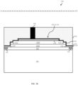
- FIG. 1A is a layout diagram and FIGs. 1B and 1C are different cross-section diagrams of an embodiment of a semiconductor structure 100 including an e-mode HEMT 110.
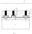
- FIG. 2A is a layout diagram and FIG. 2B is a cross-section diagram of another embodiment of a semiconductor structure 200 including alternating parallel e-mode and d-mode HEMTs (e.g., see e-mode HEMTs 210.1 and 210.2 and d-mode HEMT 280, which is without a gate, between the e-mode HEMTs).
- FIG. 3A is a layout diagram and FIG.
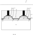
- 3B is a cross-section diagram of yet another embodiment of a semiconductor structure 300 including alternating parallel e-mode and d-mode HEMTs (e.g., see e-mode HEMTs 310.1 and 310.2 and d-mode HEMT 380 between the e-mode HEMTs).
- Each semiconductor structure 100, 200, 300 can include a substrate 101, 201, 301.
- the substrate 101, 201, 301 can be, for example, a silicon (Si) or Si-based substrate (e.g., a silicon carbide (SiC) substrate), a sapphire substrate, a III-V semiconductor substrate (e.g., a GaN substrate or some other suitable III-V semiconductor substrate) or any other suitable substrate for a III-V semiconductor device.
- III-V semiconductor refers to a compound obtained by combining group III elements, such as aluminum (Al), gallium (Ga), or indium (In), with group V elements, such as nitrogen (N), phosphorous (P), arsenic (As) or antimony (Sb) (e.g., GaN, InP, GaAs, or GaP).
- group III elements such as aluminum (Al), gallium (Ga), or indium (In)
- group V elements such as nitrogen (N), phosphorous (P), arsenic (As) or antimony (Sb) (e.g., GaN, InP, GaAs, or GaP).
- Each semiconductor structure 100, 200, 300 can further include multiple epitaxially grown semiconductor layers on the substrate 101, 201, 301.
- These semiconductor layers can include, for example: an optional buffer layer (not specifically shown) on the top surface of the substrate 101, 201, 301; a channel layer 102, 202, 302 for HEMT(s) on the buffer layer (or substrate); and a barrier layer 103, 203, 303 for HEMT(s) on the channel layer 102, 202, 302.
- These epitaxial grown semiconductor layers can be, for example, III-V semiconductor layers.
- the optional buffer layer can be employed to facilitate growth of the channel layer 102, 202, 302 and to provide for lattice constants of the substrate 101, 201, 301 below and the channel layer 102, 202, 302 above.
- the buffer layer can be doped or undoped.
- the buffer layer can be carbon-doped.
- the barrier layer 103, 203, 303 can have a band gap that is wider than the bandgap of the channel layer 102, 202, 202 for the device channel.
- barrier and channel materials can be selected so that a heterojunction is formed at the interface between the two layers, thereby resulting in the formation of a two-dimensional electron gas (2DEG) in the channel layer 102, 202, 202.
- This 2DEG in the channel layer 102, 202, 302 can provide the conductive pathway for the drifting of charges between the source and the drain.
- the buffer layer could be a carbon-doped gallium nitride (C-GaN) buffer layer or a buffer layer of any other material suitable for use as a buffer layer of a HEMT.
- the channel layer 102, 202, 302 could be a GaN layer or a III-V semiconductor layer made of any other III-V semiconductor compound suitable for use as a channel layer in a HEMT.
- the barrier layer 103, 203, 303 could be an aluminum gallium nitride (AlGaN) barrier layer or a barrier layer of any other material suitable for use as a barrier layer in a HEMT.
- the figures and the description above depict the epitaxially grown semiconductor layers (e.g., the buffer layer (not shown); the channel layer 102, 202, 302; and the barrier layer 103, 203, 303) as being single layered structures (i.e., comprising one layer of buffer material, one layer of channel material and one layer of barrier material).
- the epitaxially grown layers could be multi-layered structures (e.g., comprising multiple sub-layers of different buffer materials, multiple sub-layers of different III-V semiconductor channel materials and/or multiple sub-layers of different barrier materials).
- Each semiconductor structure 100, 200, 300 can include at least one e-mode HEMT 110, 210.1-210.2, 310.1-310.2.
- Each e-mode HEMT 110, 210.1-210.2, 310.1-310.2 can include: source and drain terminals 121-122, 221-222, 321-322; an active device region 105, 205.1-205.2, 305.1-305.2 including a corresponding section of the channel layer 102, 202, 302 extending laterally between the source and drain terminals 121-122, 221-222, 321-322; and a corresponding e-mode HEMT gate 130, 230.1-230.2, 330.1-330.2, which is on a section of the barrier layer 103, 203, 303 and which traverses the active device region 105, 205.1-205.2, 305.1-305.2 parallel to and positioned laterally between the source and drain terminals 121-122, 221-222, 321-322.
- the gate 130, 230.1-230.2, 330.1-330.2 of each e-mode HEMT 110, 210.1-210.2, 310.1-310.2 can include a semiconductor layer 132, 232, 332 on a section of the barrier layer 103. More specifically, within each e-mode HEMT, a section of the barrier layer 103, 203, 303 can include a first barrier portion 103T, 203T, 303T (also referred to herein as a thick barrier portion) and second barrier portions 103t, 203t, 303t (also referred to herein as thin barrier portions).
- the first barrier portion 103T, 203T, 303T can be positioned laterally between and can be thicker than the second barrier portions 103t, 203t, 303t. Additionally, the first barrier portion 103T, 203T, 303T can traverse the active device region and the second barrier portions 103t, 203t, 303t can extend laterally from opposing ends of the first barrier portion 103T, 203T, 303T beyond the side boundaries of the active device region.
- the semiconductor layer 132, 232, 332 can be a monocrystalline P-type III-V semiconductor layer. For example, the semiconductor layer 132, 232, 332 can be a Mg-doped GaN layer.
- the semiconductor layer 132, 232, 332 can include, above the first barrier portion 103T, 203T, 303T, a first semiconductor portion 132T, 232T, 332T (also referred to herein as a thick semiconductor portion) that is narrower in width than the first barrier portion 103T, 203T, 303T and second semiconductor portions 132t, 232t, 332t (also referred to herein as thin semiconductor portions).
- the first semiconductor portion 132T, 232T, 332T can be positioned laterally between and thicker than second semiconductor portions 132t, 232t, 332t.
- essentially vertical surfaces of the second semiconductor portions 132t, 232t, 332t can be aligned with essentially vertical of the first barrier portion 103T, 203T, 303T below such that the second barrier portions 103t, 203t, 303t extend laterally beyond the semiconductor layer 132, 232, 332.
- the gate 130, 230.1-230.2, 330.1-330.2 of each e-mode HEMT can further include a gate conductor layer 133, 233, 333 on the first semiconductor portion 132T, 232T, 332T.
- the gate conductor layer 133, 233, 333 can include metal(s) or metal alloy(s) that will form such a Schottky contact (i.e., a potential energy barrier for electrons) at the gate conductor-semiconductor.
- Metals or metal alloys that could be employed for a Schottky contact gate terminal include, but are not limited to, gold (Au), titanium (Ti), titanium nitride (TiN), nickel-gold (Ni-Au), or titanium-platinum-gold (Ti/Pt/Au).
- the gate conductor layer 133, 233, 333 can be narrower in width that the first semiconductor portion 132T, 232T, 332T below (i.e., the first semiconductor portion can be wider than the gate conductor layer) such that the first semiconductor portion 132T, 232T, 332T extends laterally beyond the gate conductor layer 133, 233, 333 toward to the side boundaries of the active device region.
- the e-mode HEMT could, more specifically, be an e-mode metal-insulator-semiconductor HEMT (MISHEMT).
- the gate of each e-mode MISHEMT could further include a gate dielectric layer (not shown) in the stack below the gate conductor layer.
- the gate dielectric layer could be a silicon dioxide (SiO 2 ) layer, a high K dielectric layer or a layer of any other dielectric material suitable for use as a gate dielectric layer of a MISHEMT
- the gate conductor layer could include one layer or multiple sub-layers of any suitable gate conductor material (e.g., gate metal(s), gate metal alloy(s), doped polysilicon, etc.).
- each end wall of the gate has a step down from the gate conductor layer 133, 233, 333 to the top surface of the first semiconductor portion 132T, 232T, 332T, another step down to the top surface of the second semiconductor portion 132t, 232t, 332t, and another step down to the top surface of the second barrier portion 103t, 203t, 303t. Since the second barrier portions 103t, 203t, 303t at the ends of the gate are relatively thin, charge build up in the channel layer at the ends of the gate is minimal or eliminated, potentially eliminating any current path around the gate.
- each e-mode HEMT can further include isolation regions 141, 241, 341 in the channel layer 102, 202, 302 aligned below areas of the second barrier portions 103t, 203t, 303t, respectively, adjacent but offset from the opposing end walls of the gate 130, 230.1-230.2, 330.1-330.2 and, thereby offset from the semiconductor layer 132, 232, 332.
- the isolation regions 141, 241, 341 can be areas of the channel layer that contain and, particularly, that have been doped a dopant, such as argon, to eliminate charge build up and thereby block potential current path(s) between the source and drain terminals 121-122, 221-222, 321-322 that would otherwise bypass the portion of the channel layer below the gate by wrapping around the end(s) of the gate.
- Doping of the doped region e.g., the argon-doped region
- implant isolation regions can be achieved, for example, using a dopant implantation process, such that the isolation regions are also referred to herein as implant isolation regions. It should be noted that, since charge build up will be limited due to the second barrier portions being relatively thin, the depth of the implant isolation regions can be relatively shallow.
- the implant isolation regions can be formed so that they are completely offset from the gate and, particularly, from the semiconductor layer therein so as to avoid any gate degradation that could be caused by a dopant implantation process, thereby ensuring that the gate remains robust (i.e., less likely to suffer from reliability issues).
- Each e-mode HEMT 110, 210.1-210.2, 310.1-310.2 can further include a conformal dielectric layer 151, 251, 351 (e.g., a conformal silicon nitride (SiN) layer or a conformal layer of some other suitable dielectric material) over the gate 130, 230.1-230.2, 330.1-330.2.
- a conformal dielectric layer 151, 251, 351 e.g., a conformal silicon nitride (SiN) layer or a conformal layer of some other suitable dielectric material
- each e-mode HEMT 110, 210.1-210.2, 310.1-310.2 can further include source and drain terminals 121-122, 221-222, 321-322 parallel to and on opposing sides of the gate 130, 230.1-230.2, 330.1-330.2.
- the source and drain terminals 121-122, 221-222, 321-322 can be separated from the gate by essentially the same separation distances or by different separation distances (e.g., as illustrated, the drain terminal 122, 222, 322 can be separated from the gate by a greater separation distance than the source terminal 121, 221, 321 for increased breakdown voltage).
- the source and drain terminals 121-122, 221-222, 321-322 can, for example, include ohmic contact source and drain terminals in source/drain openings that extend through the dielectric layer 151, 251, 351 and into the barrier layer 103, 203, 303 toward or to the channel layer 102, 202, 302. That is, the source/drain openings can extend through the dielectric layer and at least partially through the barrier layer toward the channel layer.
- the source and drain terminals can be essentially T-shaped, each with a lower section in a source/drain opening and an upper section on and wider than the lower section (e.g., extending laterally onto the dielectric layer), as illustrated.
- Such ohmic contact source and drain terminals can include one or more layers of metal or metal alloys (e.g., such ohmic contact source and drain terminals include, but are not limited to, multi-layer structures of Ti/Al/TiN, Ti/Al/Ti/Au or Mo/Al/Mo/Au). It should be noted that the source and drain terminal configurations are provided above for illustration purposes and are not intended to be limiting. Alternatively, any other suitable source and drain terminal configuration for a HEMT could be employed.
- the semiconductor structure 100 include an e-mode HEMT 110 with a gate 130 positioned laterally between discrete source and drain terminals 121-122.
- Interlayer dielectric (ILD) material 152 can cover the e-mode HEMT 110.
- the ILD material 152 can include, for example, one or more layers of dielectric material (e.g., silicon dioxide (SiO 2 ) or some other suitable ILD material).
- Contacts e.g., gate contact(s) 199 and source and drain contacts 198
- the semiconductor structure 200, 300 can include multiple HEMTs connected in parallel with shared source and drain terminals 221-222, 321-322.
- the semiconductor structure 200, 300 can include alternating e-mode HEMTs 210.1-210.2, 310.1-310.2, as described above, and d-mode HEMT(s) 280, 380.
- the barrier layer 203, 303 can include alternating first barrier portions 203T, 303T and second barrier portions 203t, 303t with each first barrier portion 203T, 303T being positioned laterally between and thicker than two adjacent second barrier portions 203t, 303T.
- the e-mode HEMTs 210.1-210.2, 310.1-310.2 can include gates 230.1-230.2, 330.1-330.2 on first barrier portions 203T, 303T, as discussed in detail above.
- Each d-mode HEMT e.g., see d-mode HEMTs 280, 380
- the d-mode HEMT 280 can include a corresponding active device region 206 in a section of the channel layer 202 positioned laterally between the active device regions 205.1 and 205.2 of the e-mode HEMTs 210.1-210.2 and extending between the source and drain terminals 221-222.
- a second barrier portion 203 T can traverse the active device region 206 and the conformal dielectric layer 251 can cover the second barrier portion 203T.
- the d-mode HEMT 280 can be devoid of a gate and, thus, always in an ON state.
- ILD material 252 can cover the various e-mode and d-mode HEMTs.
- the ILD material 252 can include, for example, one or more layers of dielectric material (e.g., SiO 2 or some other suitable ILD material). Contacts can extend through the ILD material 252 to the e-mode HEMT gates and to the source and drain terminals.
- dielectric material e.g., SiO 2 or some other suitable ILD material.
- the d-mode HEMT 380 can similarly include a corresponding active device region 306 in a section of the channel layer 302 positioned laterally between the active device regions 305.1 and 305.2 of the e-mode HEMTs 310.1-310.2 and extending between the source and drain terminals 321-322.
- a second barrier portion 303T can traverse the active device region 306 and the conformal dielectric layer 351 can cover the second barrier portion 303T.
- the d-mode HEMT 380 can include a gate 386 (referred to herein as an additional gate or a d-mode HEMT gate) to control the ON/OFF state of the d-mode HEMT 380.
- the gate 386 can be on the conformal dielectric layer 351 aligned above a second barrier portion 303T and positioned laterally between gates 330.1-330.2 (i.e., between the gates of two e-mode HEMTs 310.1-310.2).
- the gate 386 can include a gate conductor layer 383 on the second barrier portion 303T.
- the gate conductor layer 383 can include the same gate conductor material(s) as that used for the e-mode HEMT gates or, alternatively, can include different gate conductor material(s).
- ILD material 352 can cover the various e-mode and d-mode HEMTs.
- the ILD material 352 can include, for example, one or more layers of dielectric material (e.g., SiO 2 or some other suitable ILD material). Contacts can extend through the ILD material 352 to the e-mode and d-mode HEMT gates and to the source and drain terminals.
- dielectric material e.g., SiO 2 or some other suitable ILD material.
- the semiconductor structure 200 and 300 are shown as including a single d-mode HEMT between and sharing source and drain terminals with two e-mode HEMTs. However, it should be understood that the figures are not intended to be limiting. Alternatively, the semiconductor structures 200 and 300 could include any number of alternating e-mode and d-mode HEMTs.
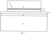
- Each of the disclosed method embodiments can include forming a stack of epitaxially grown semiconductor layers on a substrate 101, 201, 301, as illustrated in FIG. 4 .
- the substrate 101, 201, 301 can be, for example, a Si or Si-based substrate (e.g., a SiC substrate), a sapphire substrate, a III-V semiconductor substrate (e.g., a GaN substrate or some other suitable III-V semiconductor substrate) or any other suitable substrate for a III-V semiconductor device.
- the multiple epitaxially grown semiconductor layers can include, for example: an optional buffer layer (not specifically shown) on the top surface of the substrate 101, 201, 301; a channel layer 102, 202, 302 for HEMT(s) on the buffer layer (or substrate); and a barrier layer 103, 203, 303 for HEMT(s) on the channel layer 102, 202, 302.
- These epitaxial grown semiconductor layers can be, for example, III-V semiconductor layers.
- III-V semiconductor refers to a compound obtained by combining group III elements, such as Al, Ga, or In, with group V elements, such as N, P, As, or Sb (e.g., GaN, InP, GaAs, or GaP).
- the buffer layer could be a C-GaN buffer layer or a buffer layer of any other material suitable for use as a buffer layer of a HEMT.
- the channel layer 102, 202, 302 could be a GaN layer or a III-V semiconductor channel layer made of any other III-V semiconductor compound suitable for use as a channel layer in a HEMT.
- the barrier layer 103, 203, 303 could be a AlGaN barrier layer or a barrier layer of any other material suitable for use as a barrier layer in a HEMT.
- the figures and the description above depict the epitaxially grown semiconductor layers (e.g., the buffer layer (not shown); the channel layer 102, 202, 302; and the barrier layer 103, 203, 303) as being single layered structures (i.e., comprising one layer of buffer material, one layer of channel material and one layer of barrier material).
- the epitaxially grown layers could be multi-layered structures (e.g., comprising multiple sub-layers of different buffer materials, multiple sub-layers of different III-V semiconductor channel materials and/or multiple sub-layers of different barrier materials).
- These epitaxially grown semiconductor layers can also include a monocrystalline P-type III-V semiconductor layer 132, 232, 332 (e.g., a Mg-doped GaN layer) for e-mode HEMT gates to be formed during subsequent processing.
- a monocrystalline P-type III-V semiconductor layer 132, 232, 332 e.g., a Mg-doped GaN layer
- a gate conductor layer 133 can be formed on the semiconductor layer 132, as illustrated in FIG. 5 .
- the gate conductor layer 133 can include metal(s) or metal alloy(s) that will form such a Schottky contact (i.e., a potential energy barrier for electrons) at the gate conductor-semiconductor.
- Metals or metal alloys that could be employed for a Schottky contact gate terminal include, but are not limited to, Au, Ti, TiN, Ni-Au, or Ti/Pt/Au.
- a mask 501 e.g., a hardmask layer, such as a silicon nitride (SiN) hardmask layer
- a hardmask layer such as a silicon nitride (SiN) hardmask layer
- Exposed portions of the gate conductor layer 133-semiconductor layer 132 stack can then be removed (e.g., by one or more selective anisotropic etch processes) to form a gate 130 that extends laterally across the active device region.
- a timed isotropic etch process that is selective for the gate conductor material e.g., a timed wet etch process that is selective for TiN
- a timed wet etch process that is selective for TiN can be performed to laterally etch back the exposed vertical surfaces of the gate conductor material so that edges of the semiconductor layer 132 are exposed, as illustrated in FIG. 6 .
- the mask 501 can then be removed.
- An additional masked etch process can be performed to remove end sections of the gate conductor layer 133 of the gate 130, as illustrated in FIGs. 7 and 8 .
- a mask 701 e.g., another hardmask layer
- mask 701 formation can be concurrent with mask formation for patterning resistors elsewhere on the substrate and formed of the same metal or metal alloy material (e.g., TiN) as that used for the gate conductor layer 133.
- An anisotropic etch process can be performed to remove the exposed end sections of the gate conductor layer 133.
- the etch specifications used can be non-selective for the gate conductor material such that exposed surfaces of the semiconductor layer 132 and barrier layer 103 are concurrently recessed, thereby modifying the gate so that it has stepped opposing end walls, as illustrated in FIG. 8 .
- Such an etch process could be, for example, a reactive ion etch (RIE) process performed using chlorine (Cl).
- RIE reactive ion etch
- Cl chlorine
- the semiconductor layer 132 has, above the first barrier portion 103T, a first semiconductor portion 132T positioned laterally between and thicker than second semiconductor portions 132T, and the gate conductor layer 133 is on but narrower in width than the first semiconductor portion 132T.
- the mask 701 can then be selectively removed.
- isolation regions 141 can be formed, as illustrated in FIG. 9 .
- a mask 901 e.g., another hardmask layer
- a dopant implantation process can be performed to implant a dopant, such as argon, into an area of the channel layer 102 aligned below the openings 902 and completely offset from the semiconductor layer 132, thereby forming the isolation regions 141.
- isolation regions 141 can eliminate charge build up in the channel layer 102 near the ends of the gate 130 to block potential current paths around the gate 130. Since charge build up will be limited because the portions of the barrier layer 103 that extend beyond the ends of the gate 130 are relatively thin, the depth of the isolation regions 141 can be relatively shallow. Furthermore, since the mask 901 protects the semiconductor layer 132 during the dopant implantation process, gate degradation is avoided and the gate 130 remains robust (i.e., less likely to suffer from reliability issues). The mask 901 can then be removed.
- Additional processing can be performed in order to complete the e-mode HEMT 110, as illustrated in FIGs. 1A-1C .
- a conformal dielectric layer 151 e.g., a conformal SiN layer or a conformal layer of some other suitable dielectric material
- source and drain terminals 121-122 can also be formed.
- formation of the source and drain terminals 121-122 can include forming source and drain openings (e.g., using lithographic patterning and etch processes). The source and drain openings can be formed so that they are parallel to and on opposing sides of the gate 130 (e.g., separated from the gate by the same separation distance or by different separation distances).
- the source and drain openings can be formed so that they that extend through the dielectric layer 151 and into the barrier layer 103 toward or to the channel layer 102.
- One or more layers of metal or metal alloys can then be deposited over the partially completed structure so as to fill the openings. These layers can be selected to form ohmic contact source and drain terminals and can include, for example, Ti/Al/TiN, Ti/Al/Ti/Au or Mo/Al/Mo/Au.
- the stack of metal or metal alloy layers can then be patterned (e.g., lithographically patterned and etched) to form the discrete source and drain terminals 121-122 (e.g., T-shaped source and drain terminals).
- any other suitable technique for forming source and drain terminals could be employed.
- one or more layers of ILD material 152 can be deposited over the partially completed structure and contacts (e.g., gate contact(s) 199 and source and drain contacts 198) can be formed so that they extend through the ILD material 152 to the gate and source and drain terminals.
- contacts e.g., gate contact(s) 199 and source and drain contacts 198
- a gate conductor layer 233, 333 can be formed on the semiconductor layer 232, 332 and, as illustrated in FIG. 10 , the gate conductor layer-semiconductor layer stack can be lithographically patterned and etched to form discrete gates 230.1-230.2, 330.1-330.2 extending laterally across designated e-mode HEMT active device regions, respectively.
- the gates can, for example, be patterned so as to be in end-to-end alignment with each pair of adjacent gates being separated by a d-mode HEMT active device region.
- the gate conductor layer 233, 333 can include metal(s) or metal alloy(s) that will form such a Schottky contact (i.e., a potential energy barrier for electrons) at the gate conductor-semiconductor.
- Metals or metal alloys that could be employed for a Schottky contact gate terminal include, but are not limited to, Au, Ti, TiN, Ni-Au, or Ti/Pt/Au. Additionally, in the same manner as described above with regard to formation of the gate 130 in the semiconductor structure 100 of FIGs.
- exposed vertical surfaces of the gate conductor material in each gate 230.1-230.2, 330.1-330.2 can also be laterally etched (e.g., using a timed selective isotropic etch process) so that edges of the semiconductor layer 232, 332 below are slightly exposed.
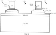
- An additional masked etch process can be performed to remove the end sections of the gate conductor layer 233, 333 of each of the gates 230.1-230.2, 330.1-330.2, as illustrated in FIGs. 11 and 12 .
- a mask layer e.g., a hardmask layer, such as a SiN hardmask layer
- mask sections 1101 are on the center of the gate conductor layer 233, 333 of each of the gates 230.1-230.2, 330.1-330.2 and so openings 1102 expose end sections and surfaces of the semiconductor layer 232, 332 and barrier layer 203, 303 that extend laterally beyond those end sections (including the portion of the barrier layer between adjacent gates).
- An anisotropic etch process (e.g., an RIE process performed using Cl) can be performed to remove the exposed end sections of the gate conductor layers.
- the etch specifications used can be non-selective for the gate conductor material such that exposed surfaces of the semiconductor layer 232, 332 and barrier layer 203, 303 are concurrently recessed, thereby modifying each gate 230.1-230.2, 330.1-330.2 so that it has stepped opposing end walls, as illustrated in FIG. 12 .
- isolation regions 241, 341 can be formed, as illustrated in FIG. 13 .
- a mask 1301 e.g., another hardmask layer
- openings 1302 that expose only areas in the thin portions of the barrier layer 203, 303 are beyond but adjacent to the opposing end walls of the gates.
- a center area of a thin portion of the barrier layer that extends between adjacent gates can remain covered by the mask.
- a dopant implantation process can be performed to implant a dopant, such as argon, into areas of the channel layer 202, 302 aligned below the openings 1302, thereby forming isolation regions 241, 341.
- a dopant such as argon
- isolation regions 241, 241 can eliminate charge build-up in the channel layer near the ends of the gates 230.1-230.2, 330.1-330.2 to block potential current paths around the gates. Since charge build up will be limited because the portions of the barrier layer that extend beyond the end walls of the gates are relatively thin, the depth of the isolation regions can be relatively shallow.
- the mask 1301 protects the semiconductor layer within each gate, gate degradation is avoided and the gates 230.1-230.2, 330.1-330.2 remain robust (i.e., less likely to suffer from reliability issues). The mask 1301 can then be removed.
- Additional processing can be performed in order to complete the e-mode HEMTs 230.1-230.2, 330.1-330.2 and the d-mode HEMT 280, 380 therebetween, as illustrated in FIGs. 2A-2B and 3A-3B .
- a conformal dielectric layer 251, 351 e.g., a conformal SiN layer or a conformal layer of some other suitable dielectric material
- a d-mode HEMT gate 386 can be formed (e.g., deposited and patterned) on the top surface of the dielectric layer 351 between the gates 330.1-330.2.
- the gate 386 can include a gate conductor layer 383 of the same gate conductor material(s) as that used for the e-mode HEMT gates or, alternatively, can include different gate conductor material(s).
- shared source and drain terminals 221-222, 321-322 for the e-mode HEMTs 210.1-210.2, 310.1-310.2 and for the d-mode HEMT 280, 380 therebetween can be formed.
- shared source and drain terminals 221-222, 321-322 can be formed, for example, in the same manner as the source and drain terminals 121-122 described in detail above.
- one or more layers of ILD material 252, 352 can be deposited over the partially completed structure and contacts can be formed so that they extend through the ILD material 252, 352 to the gates and source and drain terminals of the HEMTs.
- a semiconductor material refers to a material whose conducting properties can be altered by doping with an impurity.
- semiconductor materials include, for example, silicon-based semiconductor materials (e.g., silicon, silicon germanium, silicon germanium carbide, silicon carbide, etc.) and III-V compound semiconductors (i.e., compounds obtained by combining group III elements, such as aluminum (Al), gallium (Ga), or indium (In), with group V elements, such as nitrogen (N), phosphorous (P), arsenic (As) or antimony (Sb) (e.g., GaN, InP, GaAs, or GaP).
- group III elements such as aluminum (Al), gallium (Ga), or indium (In)
- group V elements such as nitrogen (N), phosphorous (P), arsenic (As) or antimony (Sb)
- group III elements such as aluminum (Al), gallium (Ga), or indium (In)
- group V elements such as nitrogen (N), phosphorous (P
- a pure semiconductor material and, more particularly, a semiconductor material that is not doped with an impurity for the purposes of increasing conductivity is referred to in the art as an intrinsic semiconductor.
- a semiconductor material that is doped with an impurity for the purposes of increasing conductivity is referred to in the art as an extrinsic semiconductor and will be more conductive than an intrinsic semiconductor made of the same base material. That is, extrinsic silicon will be more conductive than intrinsic silicon; extrinsic silicon germanium will be more conductive than intrinsic silicon germanium; and so on.
- a silicon-based semiconductor material e.g., silicon, silicon germanium, etc.
- a Group III dopant such as boron (B) or indium (In)
- a silicon-based semiconductor material is typically doped a Group V dopant, such as arsenic (As), phosphorous (P) or antimony (Sb), to achieve N-type conductivity.
- a gallium nitride (GaN)-based semiconductor material is typically doped with magnesium (Mg) to achieve P-type conductivity and with silicon (Si) or oxygen to achieve N-type conductivity.
- Mg magnesium
- Si silicon
- oxygen oxygen
- different conductivity levels will depend upon the relative concentration levels of the dopant(s) in a given semiconductor region.
- a semiconductor region or layer is described as being at a higher conductivity level than another semiconductor region or layer, it is more conductive (less resistive) than the other semiconductor region or layer; whereas, when a semiconductor region or layer is described as being at a lower conductivity level than another semiconductor region or layer, it is less conductive (more resistive) than that other semiconductor region or layer.
- laterally is used herein to describe the relative locations of elements and, more particularly, to indicate that an element is positioned to the side of another element as opposed to above or below the other element, as those elements are oriented and illustrated in the drawings.
- an element that is positioned laterally adjacent to another element will be beside the other element
- an element that is positioned laterally immediately adjacent to another element will be directly beside the other element
- an element that laterally surrounds another element will be adjacent to and border the outer sidewalls of the other element.
- the corresponding structures, materials, acts, and equivalents of all means or step plus function elements in the embodiments below are intended to include any structure, material, or act for performing the function in combination with other claimed elements as specifically claimed.
- various aspects of the present disclosure show a structure including an enhancement mode high electron mobility transistor (HEMT).
- the HEMT includes a barrier layer with a thick portion positioned laterally between thin portions and a gate.
- the gate includes a semiconductor layer (e.g., a P-type III-V semiconductor layer) on the thick portion of the barrier layer and having a thick portion positioned laterally between thin portions.
- the gate also includes a gate conductor layer on and narrower than the thick portion of the semiconductor layer, so end walls of the gate are stepped. Thin portions of the barrier layer near these end walls minimize or eliminate charge build up in a channel layer below.
- isolation regions can be below the thin portions of the barrier layer offset from the semiconductor layer.
- the structure can further include alternating e-mode and d-mode HEMTs. Also disclosed are associated method embodiments.
- the term "include” and its variants may be interpreted as meaning that an embodiment includes stated features, while not necessarily excluding the presence of other features that are not explicitly stated.
Landscapes
- Junction Field-Effect Transistors (AREA)
Abstract
A disclosed structure includes an enhancement mode high electron mobility transistor (HEMT). The HEMT includes a barrier layer (103) with a thick portion (103T) positioned laterally between thin portions (103t) and a gate. The gate includes a semiconductor layer (132) (e.g., a P-type III-V semiconductor layer) on the thick portion of the barrier layer and having a thick portion (132T) positioned laterally between thin portions (132t). The gate also includes a gate conductor layer (133) on and narrower than the thick portion of the semiconductor layer, so end walls of the gate are stepped. Thin portions of the barrier layer near these end walls minimize or eliminate charge build up in a channel layer below. To block current paths around the gate, isolation regions can be below the thin portions of the barrier layer offset from the semiconductor layer. The structure can further include alternating e-mode and d-mode HEMTs. Also disclosed are associated method embodiments.
Description
- This invention was made with government support under contract number HQ0727790700 and awarded by the United States Defense Microelectronics Activity (DMEA) and the United States Defense Advanced Research Projects Agency (DARPA). The government has certain rights in the invention.
- The present disclosure relates to transistors, and, more particularly, to embodiments of a semiconductor structure including an enhancement mode (e-mode) high electron mobility transistor (HEMT) with a robust gate and to embodiments of a method of forming the structure.
- HEMTs have emerged as a leading technology for radio frequency (RF) and millimeter wave (mmWave) (e.g., 3-300GHz) wireless applications. Such HEMTs are normally depletion mode (d-mode) devices that can be modified to form enhancement mode (e-mode) devices. However, currently available e-mode HEMTs suffer from reliability issues.
- Disclosed herein are embodiments of a semiconductor structure. The semiconductor structure can include a barrier layer with a first barrier portion positioned laterally between and thicker than second barrier portions. The semiconductor structure can further include a gate. The gate can include a semiconductor layer and a gate conductor layer. The semiconductor layer can be on the first barrier portion and can have, above the first barrier portion, a first semiconductor portion positioned laterally between and thicker than second semiconductor portions. The gate conductor layer can be on and narrower in width than the first semiconductor portion.
- Some embodiments of the semiconductor structure disclosed herein can include a barrier layer with alternating first barrier portions and second barrier portions. Each first barrier portion can be positioned laterally between and thicker than the adjacent second barrier portions. The semiconductor structure can further include multiple gates. Each gate can include a semiconductor layer and a gate conductor layer. The semiconductor layer can be on a first barrier portion and can have, above the first barrier portion, a first semiconductor portion positioned laterally between and thicker than second semiconductor portions. The gate conductor layer can be on and narrower in width than the first semiconductor portion. The semiconductor structure can further include a conformal dielectric layer over the gates and further on the second barrier portions on opposing sides of the gates.
- Also disclosed herein are method embodiments for forming such semiconductor structures. For example, a disclosed method embodiment can include forming a barrier layer and forming a gate above the barrier layer. The gate can be formed so as to include a semiconductor layer and a gate conductor layer, as described below. The semiconductor layer can be on a first barrier portion of the barrier layer, which is between and thicker than second barrier portions. Additionally, the semiconductor layer can have, above the first barrier portion, a first semiconductor portion positioned laterally between and thicker than second semiconductor portions. The gate conductor layer can be on and narrower in width than the first semiconductor portion.
- The present disclosure will be better understood from the following detailed description with reference to the drawings, which are not necessarily drawn to scale and in which:
-
FIG. 1A is a layout diagram andFIGs. 1B and1C are different cross-section diagrams of a disclosed embodiment of a semiconductor structure; -
FIG. 2A is a layout diagram andFIG. 2B is a cross-section diagram of another disclosed embodiment of a semiconductor structure; -
FIG. 3A is a layout diagram andFIG. 3B is a cross-section diagram of yet another disclosed embodiment of a semiconductor structure; -
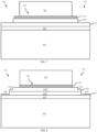
FIGs. 4-9 are cross-section diagrams illustrative of process steps in the formation of the semiconductor structure ofFIGs. 1A-1C ; and -
FIGs. 10-13 are cross-section diagrams illustrative of process steps in the formation of the semiconductor structures ofFIGs. 2A-2B and3A-3B . - As mentioned above, HEMTs, have emerged as a leading technology for RF and mm Wave wireless applications. Those skilled in the art will recognize that conventional HEMTs are typically d-mode devices. A d-mode HEMT refers to a HEMT that is normally in an ON-state (i.e., conductive) and only switches to an OFF-state (i.e., becomes non-conductive) when a voltage is applied to the gate of the HEMT. This is due to a zero-bias two-dimensional electron gas (2DEG) below the gate and, particularly, between the barrier and channel layers of the HEMT. The gate can, however, be modified to form an e-mode HEMT. An e-mode HEMT refers to HEMT that is normally in an OFF-state (i.e., non-conductive) and only switches to an ON-state (i.e., becomes conductive) when a voltage is applied to the gate. One technique for modifying the gate of a d-mode HEMT to form an e-mode HEMT is to insert a P-type III-V semiconductor layer (e.g., a magnesium (Mg)-doped gallium nitride (GaN) layer or some other suitable P-type III-V semiconductor layer) into the gate (e.g., above the barrier layer and below the gate metal) in order to suppress the zero-bias 2DEG. However, as mentioned above, currently available e-mode HEMTs suffer from reliability issues. The inventors have determined that the reliability issues stem from gate degradation caused by implant isolation region formation. Specifically, during HEMT processing, gate formation on a barrier layer is followed by formation of implant isolation region(s) in a channel layer below the barrier layer. The implant isolation region(s) are formed using a dopant implantation process so that they are located below one or both ends of the gate and so that they block potential current path(s) between the source/drain regions that would otherwise bypass the portion of the channel layer below the gate by wrapping around the end(s) of the gate. Such current path(s) are created due to charge build up in the channel layer under the barrier layer and the implant isolation region(s) effectively eliminate the charge. In e-mode HEMTs, the dopant is implanted through the P-type III-V semiconductor layer at the end(s) of the gate and, as a result, causes gate degradation and, thereby reliability issues.
- In view of the foregoing, disclosed herein are embodiments of a semiconductor structure including at least one enhancement mode (e-mode) high electron mobility transistor (HEMT) with a robust gate to minimize reliability issues. Specifically, the e-mode HEMT can include a barrier layer on a channel layer. The barrier layer can have a thick portion positioned laterally between thin portions. The e-mode HEMT can also include a gate. The gate can be positioned laterally between, separated from, and parallel to source/drain terminals and can traverse the width of an active device region. The gate can include a semiconductor layer (e.g., a P-type III-V semiconductor layer, such as an Mg-doped GaN layer) on the thick portion of the barrier layer. The semiconductor layer can include a thick portion positioned laterally between thin portions. The gate can further include a gate conductor layer on and narrower in width than the thick portion of the semiconductor layer. Thus, opposing end walls of the gate are stepped and the thin portions of the barrier layer near the end walls minimize or eliminate charge build up in the channel layer that could potentially result in a current path around the gate. As a result, implant isolation regions in the channel layer may be unnecessary. However, if necessary to block potential current paths around the gate, implant isolation regions can be aligned below the thin portions of the barrier layer. They will not need to be as deep because charge build up will be reduced due to the relatively thin barrier layer in the area. Additionally, they can be completely offset from the semiconductor layer of the gate due to the stepped end walls and, thus, gate degradation due to dopants implanted through the semiconductor layer of the gate is avoided and the gate of the HEMT remains robust. In some embodiments, the semiconductor structure can further include alternating e-mode and d-mode HEMTs with shared source and drain terminals, where the e-mode HEMTs similarly have robust gates. Also disclosed herein are method embodiments for forming the disclosed semiconductor structures.
- More particularly,
FIG. 1A is a layout diagram andFIGs. 1B and1C are different cross-section diagrams of an embodiment of asemiconductor structure 100 including ane-mode HEMT 110.FIG. 2A is a layout diagram andFIG. 2B is a cross-section diagram of another embodiment of asemiconductor structure 200 including alternating parallel e-mode and d-mode HEMTs (e.g., see e-mode HEMTs 210.1 and 210.2 and d-mode HEMT 280, which is without a gate, between the e-mode HEMTs).FIG. 3A is a layout diagram andFIG. 3B is a cross-section diagram of yet another embodiment of asemiconductor structure 300 including alternating parallel e-mode and d-mode HEMTs (e.g., see e-mode HEMTs 310.1 and 310.2 and d-mode HEMT 380 between the e-mode HEMTs). - Each
semiconductor structure substrate substrate - Each
semiconductor structure substrate substrate channel layer barrier layer channel layer channel layer substrate channel layer barrier layer channel layer channel layer channel layer - In some embodiments, the buffer layer could be a carbon-doped gallium nitride (C-GaN) buffer layer or a buffer layer of any other material suitable for use as a buffer layer of a HEMT. The
channel layer barrier layer channel layer barrier layer - Each
semiconductor structure e-mode HEMT 110, 210.1-210.2, 310.1-310.2. - Each
e-mode HEMT 110, 210.1-210.2, 310.1-310.2 can include: source and drain terminals 121-122, 221-222, 321-322; anactive device region 105, 205.1-205.2, 305.1-305.2 including a corresponding section of thechannel layer e-mode HEMT gate 130, 230.1-230.2, 330.1-330.2, which is on a section of thebarrier layer active device region 105, 205.1-205.2, 305.1-305.2 parallel to and positioned laterally between the source and drain terminals 121-122, 221-222, 321-322. - The
gate 130, 230.1-230.2, 330.1-330.2 of eache-mode HEMT 110, 210.1-210.2, 310.1-310.2 can include asemiconductor layer barrier layer 103. More specifically, within each e-mode HEMT, a section of thebarrier layer first barrier portion second barrier portions first barrier portion second barrier portions first barrier portion second barrier portions first barrier portion semiconductor layer semiconductor layer semiconductor layer first barrier portion first semiconductor portion first barrier portion second semiconductor portions first semiconductor portion second semiconductor portions second semiconductor portions first barrier portion second barrier portions semiconductor layer - The
gate 130, 230.1-230.2, 330.1-330.2 of each e-mode HEMT can further include agate conductor layer first semiconductor portion gate conductor layer gate conductor layer first semiconductor portion first semiconductor portion gate conductor layer - Optionally, the e-mode HEMT could, more specifically, be an e-mode metal-insulator-semiconductor HEMT (MISHEMT). In this case, the gate of each e-mode MISHEMT could further include a gate dielectric layer (not shown) in the stack below the gate conductor layer. The gate dielectric layer could be a silicon dioxide (SiO2) layer, a high K dielectric layer or a layer of any other dielectric material suitable for use as a gate dielectric layer of a MISHEMT In this case, the gate conductor layer could include one layer or multiple sub-layers of any suitable gate conductor material (e.g., gate metal(s), gate metal alloy(s), doped polysilicon, etc.).
- Thus, the
gate 130, 230.1-230.2, 330.1-330.2 of each e-mode HEMT has stepped opposing end walls. That is, instead of having essentially vertical opposing end walls, each end wall of the gate has a step down from thegate conductor layer first semiconductor portion second semiconductor portion second barrier portion second barrier portions - However, optionally, in order to block any such current path, each e-mode HEMT can further include
isolation regions channel layer second barrier portions gate 130, 230.1-230.2, 330.1-330.2 and, thereby offset from thesemiconductor layer isolation regions - Each
e-mode HEMT 110, 210.1-210.2, 310.1-310.2 can further include aconformal dielectric layer gate 130, 230.1-230.2, 330.1-330.2. - As mentioned above, each
e-mode HEMT 110, 210.1-210.2, 310.1-310.2 can further include source and drain terminals 121-122, 221-222, 321-322 parallel to and on opposing sides of thegate 130, 230.1-230.2, 330.1-330.2. The source and drain terminals 121-122, 221-222, 321-322 can be separated from the gate by essentially the same separation distances or by different separation distances (e.g., as illustrated, thedrain terminal source terminal dielectric layer barrier layer channel layer - As illustrated in
FIGs. 1A-1C , thesemiconductor structure 100 include ane-mode HEMT 110 with agate 130 positioned laterally between discrete source and drain terminals 121-122. Interlayer dielectric (ILD)material 152 can cover thee-mode HEMT 110. TheILD material 152 can include, for example, one or more layers of dielectric material (e.g., silicon dioxide (SiO2) or some other suitable ILD material). Contacts (e.g., gate contact(s) 199 and source and drain contacts 198) can extend through theILD material 152 to the gate and source and drain terminals. - As illustrated in
FIGs. 2A-2B andFIGs. 3A-3B , thesemiconductor structure semiconductor structure barrier layer first barrier portions second barrier portions first barrier portion second barrier portions first barrier portions mode HEMTs 280, 380) can be positioned laterally between a pair of e-mode HEMTs, as illustrated. - Referring to the
semiconductor structure 200 ofFIGs. 2A-2B , in this case, the d-mode HEMT 280 can include a correspondingactive device region 206 in a section of thechannel layer 202 positioned laterally between the active device regions 205.1 and 205.2 of the e-mode HEMTs 210.1-210.2 and extending between the source and drain terminals 221-222. Asecond barrier portion 203 T can traverse theactive device region 206 and theconformal dielectric layer 251 can cover thesecond barrier portion 203T. In this embodiment, the d-mode HEMT 280 can be devoid of a gate and, thus, always in an ON state.ILD material 252 can cover the various e-mode and d-mode HEMTs. TheILD material 252 can include, for example, one or more layers of dielectric material (e.g., SiO2 or some other suitable ILD material). Contacts can extend through theILD material 252 to the e-mode HEMT gates and to the source and drain terminals. - Referring to the
semiconductor structure 300 ofFIGs. 3A-3B , in this case, the d-mode HEMT 380 can similarly include a correspondingactive device region 306 in a section of thechannel layer 302 positioned laterally between the active device regions 305.1 and 305.2 of the e-mode HEMTs 310.1-310.2 and extending between the source and drain terminals 321-322. Asecond barrier portion 303T can traverse theactive device region 306 and theconformal dielectric layer 351 can cover thesecond barrier portion 303T. In this embodiment, the d-mode HEMT 380 can include a gate 386 (referred to herein as an additional gate or a d-mode HEMT gate) to control the ON/OFF state of the d-mode HEMT 380. Thegate 386 can be on theconformal dielectric layer 351 aligned above asecond barrier portion 303T and positioned laterally between gates 330.1-330.2 (i.e., between the gates of two e-mode HEMTs 310.1-310.2). Thegate 386 can include agate conductor layer 383 on thesecond barrier portion 303T. Thegate conductor layer 383 can include the same gate conductor material(s) as that used for the e-mode HEMT gates or, alternatively, can include different gate conductor material(s).ILD material 352 can cover the various e-mode and d-mode HEMTs. TheILD material 352 can include, for example, one or more layers of dielectric material (e.g., SiO2 or some other suitable ILD material). Contacts can extend through theILD material 352 to the e-mode and d-mode HEMT gates and to the source and drain terminals. - For purposes of illustration, the
semiconductor structure semiconductor structures - Also disclosed herein are method embodiments for forming a semiconductor structure, such as the
semiconductor structure 100 ofFIGs. 1A-1C , that includes an e-mode HEMT having a robust gate and method embodiments for forming a semiconductor structure, such as thesemiconductor structure 200 ofFIGs. 2A-2B or thesemiconductor structure 300 ofFIGs. 3A-3B , that includes alternating e-mode and d-mode HEMTs with shared source and drain terminals, where the e-mode HEMTs similarly have robust gates. - Each of the disclosed method embodiments can include forming a stack of epitaxially grown semiconductor layers on a
substrate FIG. 4 . Thesubstrate substrate channel layer barrier layer channel layer - In some embodiments, the buffer layer could be a C-GaN buffer layer or a buffer layer of any other material suitable for use as a buffer layer of a HEMT. The
channel layer barrier layer channel layer barrier layer V semiconductor layer - To form the
semiconductor structure 100 ofFIGs. 1A-1B , agate conductor layer 133 can be formed on thesemiconductor layer 132, as illustrated inFIG. 5 . Thegate conductor layer 133 can include metal(s) or metal alloy(s) that will form such a Schottky contact (i.e., a potential energy barrier for electrons) at the gate conductor-semiconductor. Metals or metal alloys that could be employed for a Schottky contact gate terminal include, but are not limited to, Au, Ti, TiN, Ni-Au, or Ti/Pt/Au. A mask 501 (e.g., a hardmask layer, such as a silicon nitride (SiN) hardmask layer) can subsequently be formed on thegate conductor layer 133 and lithographically patterned and etched into an essentially rectangular shape that extends laterally across a designated active device region. Exposed portions of the gate conductor layer 133-semiconductor layer 132 stack can then be removed (e.g., by one or more selective anisotropic etch processes) to form agate 130 that extends laterally across the active device region. Following gate formation, a timed isotropic etch process that is selective for the gate conductor material (e.g., a timed wet etch process that is selective for TiN) can be performed to laterally etch back the exposed vertical surfaces of the gate conductor material so that edges of thesemiconductor layer 132 are exposed, as illustrated inFIG. 6 . Themask 501 can then be removed. - An additional masked etch process can be performed to remove end sections of the
gate conductor layer 133 of thegate 130, as illustrated inFIGs. 7 and 8 . Specifically, a mask 701 (e.g., another hardmask layer) can be formed on thegate conductor layer 133 and lithographically patterned and etched so as to haveopenings 702 that expose the end sections of thegate conductor layer 133 as well as surfaces of thesemiconductor layer 132 andbarrier layer 103 that extend laterally beyond those end sections. It should be noted that thatmask 701 formation can be concurrent with mask formation for patterning resistors elsewhere on the substrate and formed of the same metal or metal alloy material (e.g., TiN) as that used for thegate conductor layer 133. An anisotropic etch process can be performed to remove the exposed end sections of thegate conductor layer 133. The etch specifications used can be non-selective for the gate conductor material such that exposed surfaces of thesemiconductor layer 132 andbarrier layer 103 are concurrently recessed, thereby modifying the gate so that it has stepped opposing end walls, as illustrated inFIG. 8 . Such an etch process could be, for example, a reactive ion etch (RIE) process performed using chlorine (Cl). As a result, in the area of thegate 130, thebarrier layer 103 has afirst barrier portion 103T positioned laterally between and thicker thansecond barrier portions 103T. Additionally, within thegate 130, thesemiconductor layer 132 has, above thefirst barrier portion 103T, afirst semiconductor portion 132T positioned laterally between and thicker thansecond semiconductor portions 132T, and thegate conductor layer 133 is on but narrower in width than thefirst semiconductor portion 132T. Themask 701 can then be selectively removed. - Optionally, following
gate 130 formation, isolation regions 141 (e.g., implant isolation regions) can be formed, as illustrated inFIG. 9 . Specifically, a mask 901 (e.g., another hardmask layer) can be formed over the partially completed structure and lithographically patterned and etched so as to formopenings 902 that expose only areas of thesecond barrier portions 103t that are beyond the ends ofsemiconductor layer 132. Then, a dopant implantation process can be performed to implant a dopant, such as argon, into an area of thechannel layer 102 aligned below theopenings 902 and completely offset from thesemiconductor layer 132, thereby forming theisolation regions 141. As discussed above,such isolation regions 141 can eliminate charge build up in thechannel layer 102 near the ends of thegate 130 to block potential current paths around thegate 130. Since charge build up will be limited because the portions of thebarrier layer 103 that extend beyond the ends of thegate 130 are relatively thin, the depth of theisolation regions 141 can be relatively shallow. Furthermore, since themask 901 protects thesemiconductor layer 132 during the dopant implantation process, gate degradation is avoided and thegate 130 remains robust (i.e., less likely to suffer from reliability issues). Themask 901 can then be removed. - Additional processing can be performed in order to complete the
e-mode HEMT 110, as illustrated inFIGs. 1A-1C . For example, a conformal dielectric layer 151 (e.g., a conformal SiN layer or a conformal layer of some other suitable dielectric material) can be formed over the partially completed structure. Then, source and drain terminals 121-122 can also be formed. In some embodiments, formation of the source and drain terminals 121-122 can include forming source and drain openings (e.g., using lithographic patterning and etch processes). The source and drain openings can be formed so that they are parallel to and on opposing sides of the gate 130 (e.g., separated from the gate by the same separation distance or by different separation distances). The source and drain openings can be formed so that they that extend through thedielectric layer 151 and into thebarrier layer 103 toward or to thechannel layer 102. One or more layers of metal or metal alloys can then be deposited over the partially completed structure so as to fill the openings. These layers can be selected to form ohmic contact source and drain terminals and can include, for example, Ti/Al/TiN, Ti/Al/Ti/Au or Mo/Al/Mo/Au. The stack of metal or metal alloy layers can then be patterned (e.g., lithographically patterned and etched) to form the discrete source and drain terminals 121-122 (e.g., T-shaped source and drain terminals). Alternatively, any other suitable technique for forming source and drain terminals could be employed. Then, using conventional middle of the line (MOL) processing techniques, one or more layers ofILD material 152 can be deposited over the partially completed structure and contacts (e.g., gate contact(s) 199 and source and drain contacts 198) can be formed so that they extend through theILD material 152 to the gate and source and drain terminals. - To form the
semiconductor structure 200 ofFIGs. 2A-2B or thesemiconductor structure 300 ofFIGs. 3A-3B , agate conductor layer semiconductor layer FIG. 10 , the gate conductor layer-semiconductor layer stack can be lithographically patterned and etched to form discrete gates 230.1-230.2, 330.1-330.2 extending laterally across designated e-mode HEMT active device regions, respectively. The gates can, for example, be patterned so as to be in end-to-end alignment with each pair of adjacent gates being separated by a d-mode HEMT active device region. Thegate conductor layer gate 130 in thesemiconductor structure 100 ofFIGs. 1A-1C , exposed vertical surfaces of the gate conductor material in each gate 230.1-230.2, 330.1-330.2 can also be laterally etched (e.g., using a timed selective isotropic etch process) so that edges of thesemiconductor layer - An additional masked etch process can be performed to remove the end sections of the
gate conductor layer FIGs. 11 and12 . Specifically, a mask layer (e.g., a hardmask layer, such as a SiN hardmask layer) can be formed and lithographically patterned and etched somask sections 1101 are on the center of thegate conductor layer openings 1102 expose end sections and surfaces of thesemiconductor layer barrier layer semiconductor layer barrier layer FIG. 12 . - Optionally, following gate formation,
isolation regions 241, 341 (e.g., implant isolation regions) can be formed, as illustrated inFIG. 13 . Specifically, a mask 1301 (e.g., another hardmask layer) can be formed over the partially completed structure and lithographically patterned and etched so as to haveopenings 1302 that expose only areas in the thin portions of thebarrier layer channel layer openings 1302, thereby formingisolation regions such isolation regions mask 1301 protects the semiconductor layer within each gate, gate degradation is avoided and the gates 230.1-230.2, 330.1-330.2 remain robust (i.e., less likely to suffer from reliability issues). Themask 1301 can then be removed. - Additional processing can be performed in order to complete the e-mode HEMTs 230.1-230.2, 330.1-330.2 and the d-
mode HEMT FIGs. 2A-2B and3A-3B . For example, aconformal dielectric layer 251, 351 (e.g., a conformal SiN layer or a conformal layer of some other suitable dielectric material) can be formed over the partially completed structure. Optionally, as illustrated in thesemiconductor structure 300 ofFIGs. 3A-3B , a d-mode HEMT gate 386 can be formed (e.g., deposited and patterned) on the top surface of thedielectric layer 351 between the gates 330.1-330.2. Thegate 386 can include agate conductor layer 383 of the same gate conductor material(s) as that used for the e-mode HEMT gates or, alternatively, can include different gate conductor material(s). Then, shared source and drain terminals 221-222, 321-322 for the e-mode HEMTs 210.1-210.2, 310.1-310.2 and for the d-mode HEMT ILD material ILD material - It should be understood that in the structures and method described above, a semiconductor material refers to a material whose conducting properties can be altered by doping with an impurity. Such semiconductor materials include, for example, silicon-based semiconductor materials (e.g., silicon, silicon germanium, silicon germanium carbide, silicon carbide, etc.) and III-V compound semiconductors (i.e., compounds obtained by combining group III elements, such as aluminum (Al), gallium (Ga), or indium (In), with group V elements, such as nitrogen (N), phosphorous (P), arsenic (As) or antimony (Sb) (e.g., GaN, InP, GaAs, or GaP). A pure semiconductor material and, more particularly, a semiconductor material that is not doped with an impurity for the purposes of increasing conductivity (i.e., an undoped semiconductor material) is referred to in the art as an intrinsic semiconductor. A semiconductor material that is doped with an impurity for the purposes of increasing conductivity (i.e., a doped semiconductor material) is referred to in the art as an extrinsic semiconductor and will be more conductive than an intrinsic semiconductor made of the same base material. That is, extrinsic silicon will be more conductive than intrinsic silicon; extrinsic silicon germanium will be more conductive than intrinsic silicon germanium; and so on. Furthermore, it should be understood that different impurities (i.e., different dopants) can be used to achieve different conductivity types (e.g., P-type conductivity and N-type conductivity) and that the dopants may vary depending upon the different semiconductor materials used. For example, a silicon-based semiconductor material (e.g., silicon, silicon germanium, etc.) is typically doped with a Group III dopant, such as boron (B) or indium (In), to achieve P-type conductivity, whereas a silicon-based semiconductor material is typically doped a Group V dopant, such as arsenic (As), phosphorous (P) or antimony (Sb), to achieve N-type conductivity. A gallium nitride (GaN)-based semiconductor material is typically doped with magnesium (Mg) to achieve P-type conductivity and with silicon (Si) or oxygen to achieve N-type conductivity. Those skilled in the art will also recognize that different conductivity levels will depend upon the relative concentration levels of the dopant(s) in a given semiconductor region. Furthermore, when a semiconductor region or layer is described as being at a higher conductivity level than another semiconductor region or layer, it is more conductive (less resistive) than the other semiconductor region or layer; whereas, when a semiconductor region or layer is described as being at a lower conductivity level than another semiconductor region or layer, it is less conductive (more resistive) than that other semiconductor region or layer.
- It should be understood that the terminology used herein is for the purpose of describing the disclosed structures and methods and is not intended to be limiting. For example, as used herein, the singular forms "a," "an" and "the" are intended to include the plural forms as well, unless the context clearly indicates otherwise. Additionally, as used herein, the terms "comprises," "comprising," "includes" and/or "including" specify the presence of stated features, integers, steps, operations, elements, and/or components, but do not preclude the presence or addition of one or more other features, integers, steps, operations, elements, components, and/or groups thereof. Furthermore, as used herein, terms such as "right," "left," "vertical," "horizontal," "top," "bottom," "upper," "lower," "under," "below," "underlying," "over," "overlying," "parallel," "perpendicular," etc., are intended to describe relative locations as they are oriented and illustrated in the drawings (unless otherwise indicated) and terms such as "touching," "in direct contact," "abutting," "directly adjacent to," "immediately adjacent to," etc., are intended to indicate that at least one element physically contacts another element (without other elements separating the described elements). The term "laterally" is used herein to describe the relative locations of elements and, more particularly, to indicate that an element is positioned to the side of another element as opposed to above or below the other element, as those elements are oriented and illustrated in the drawings. For example, an element that is positioned laterally adjacent to another element will be beside the other element, an element that is positioned laterally immediately adjacent to another element will be directly beside the other element, and an element that laterally surrounds another element will be adjacent to and border the outer sidewalls of the other element. The corresponding structures, materials, acts, and equivalents of all means or step plus function elements in the embodiments below are intended to include any structure, material, or act for performing the function in combination with other claimed elements as specifically claimed.
- The descriptions of the various disclosed embodiments have been presented for purposes of illustration and are not intended to be exhaustive or limiting. Many modifications and variations will be apparent to those of ordinary skill in the art without departing from the scope and spirit of the disclosed embodiments. The terminology used herein was chosen to best explain the principles of the embodiments, the practical application or technical improvement over technologies found in the marketplace, or to enable others of ordinary skill in the art to understand the embodiments disclosed herein.
- In summary, various aspects of the present disclosure show a structure including an enhancement mode high electron mobility transistor (HEMT). The HEMT includes a barrier layer with a thick portion positioned laterally between thin portions and a gate. The gate includes a semiconductor layer (e.g., a P-type III-V semiconductor layer) on the thick portion of the barrier layer and having a thick portion positioned laterally between thin portions. The gate also includes a gate conductor layer on and narrower than the thick portion of the semiconductor layer, so end walls of the gate are stepped. Thin portions of the barrier layer near these end walls minimize or eliminate charge build up in a channel layer below. To block current paths around the gate, isolation regions can be below the thin portions of the barrier layer offset from the semiconductor layer. The structure can further include alternating e-mode and d-mode HEMTs. Also disclosed are associated method embodiments.
- The various aspects of the present disclosure may be exemplified in the following embodiments which are explicitly disclosed:
- Embodiment 1:
A structure comprising:- a barrier layer having one first barrier portion and second barrier portions, wherein the first barrier portion is positioned laterally between and thicker than the second barrier portions; and
- a gate including:
- a semiconductor layer on the first barrier portion, wherein the semiconductor layer has, above the first barrier portion, a first semiconductor portion and second semiconductor portions and wherein the first semiconductor portion is positioned laterally between and thicker than the second semiconductor portions; and
- a gate conductor layer on the first semiconductor portion, wherein the first semiconductor portion is wider than the gate conductor layer.
- Embodiment 2:
The structure of embodiment 1, further comprising:- a channel layer, wherein the barrier layer is on the channel layer; and
- isolation regions in the channel layer below the second barrier portions.
- Embodiment 3:
The structure of embodiment 2, wherein the isolation regions include argon-doped regions. - Embodiment 4:
The structure of embodiment 2 or 3, wherein the isolation regions are offset from the semiconductor layer. - Embodiment 5:
The structure of one of embodiments 1 to 4, wherein the semiconductor layer includes a P-type III-V semiconductor layer. - Embodiment 6:
The structure of one of embodiments 1 to 5,- wherein the barrier layer includes an aluminum gallium nitride layer,
- wherein the semiconductor layer includes a magnesium-doped gallium nitride layer, and
- wherein the gate conductor layer includes a titanium nitride layer.
- Embodiment 7:
The structure of one of embodiments 1 to 6, further comprising:- a source terminal extending at least partially through the barrier layer toward a channel layer; and
- a drain terminal extending at least partially through the barrier layer toward the channel layer,
- wherein the gate is positioned laterally between the source terminal and the drain terminal.
- Embodiment 8:
A structure comprising:- a barrier layer with alternating first barrier portions and second barrier portions, wherein each first barrier portion is positioned laterally between and thicker than adjacent second barrier portions;
- gates, each gate including:
- a semiconductor layer on a first barrier portion, wherein the semiconductor layer has, above the first barrier portion, a first semiconductor portion and second semiconductor portions and wherein the first semiconductor portion is positioned laterally between and thicker than the second semiconductor portions; and
- a gate conductor layer on the first semiconductor portion, wherein the first semiconductor portion is wider than the gate conductor layer; and
- a conformal dielectric layer over the gates and further on the second barrier portions on opposing sides of the gates.
- Embodiment 9
The structure of embodiment 8, further comprising:- a channel layer, wherein the barrier layer is on the channel layer; and
- isolation regions in the channel layer below the second barrier portions.
- Embodiment 10:
The structure of embodiment 9, wherein the isolation regions include argon-doped regions. - Embodiment 11:
The structure of embodiment 9 or 10, wherein the isolation regions are offset from the semiconductor layer of each gate. - Embodiment 12:
The structure of one of embodiments 8 to 11, wherein the semiconductor layer of each gate includes a P-type III-V semiconductor layer. - Embodiment 13:
The structure of one of embodiments 8 to 12,- wherein the barrier layer includes an aluminum gallium nitride layer,
- wherein the semiconductor layer of each gate includes a magnesium-doped gallium nitride layer, and
- wherein the gate conductor layer of each gate includes a titanium nitride layer.
- Embodiment 14:
The structure of one of embodiments 8 to 13, further comprising:- a source terminal extending at least partially through the barrier layer toward a channel layer; and
- a drain terminal extending at least partially through the barrier layer toward the channel layer,
- wherein the gates are positioned laterally between the source terminal and the drain terminal.
- Embodiment 15:
The structure of one of embodiments 8 to 14, further comprising: an additional gate on the conformal dielectric layer aligned above a second barrier portion between two of the gates. - Embodiment 16:
A method comprising:- forming a barrier layer; and
- forming a gate including:
- a semiconductor layer on the barrier layer,
- wherein the barrier layer has a first barrier portion and second barrier portions,
- wherein the first barrier portion is positioned laterally between and thicker than the second barrier portions,
- wherein the semiconductor layer has, above the first barrier portion, a first semiconductor portion and second semiconductor portions, and
- wherein the first semiconductor portion is positioned laterally between and thicker than the second semiconductor portions; and
- a gate conductor layer on the first semiconductor portion, wherein the first semiconductor portion is wider than the gate conductor layer.
- a semiconductor layer on the barrier layer,
- Embodiment 17:
The method of embodiment 16, wherein the forming of the gate includes:- forming the semiconductor layer on the barrier layer;
- forming the gate conductor layer on the semiconductor layer to form a gate conductor layer-semiconductor layer stack;
- patterning the gate conductor layer-semiconductor layer stack;
- laterally etching vertical surfaces of the gate conductor layer to expose edge portions of the semiconductor layer;
- forming a mask layer on the gate conductor layer so end sections of the gate conductor layer are exposed; and
- etching away the end sections of the gate conductor layer and concurrently recessing exposed surfaces of the second semiconductor portions and the second barrier portions.
- Embodiment 18:
The method of embodiment 17, wherein the barrier layer is above a channel layer and wherein the method further includes forming isolation regions in the channel layer below the second barrier portions, respectively. - Embodiment 19:
The method of embodiment 18, wherein the forming of the isolation regions includes forming implant isolation regions offset from the semiconductor layer. - Embodiment 20:
The method of one of embodiments 17 to 19, wherein the semiconductor layer comprises a P-type III-V semiconductor layer. - Embodiment 21:
A structure comprising:- a barrier layer having at least one first barrier portion and second barrier portions, wherein the at least one first barrier portion is positioned laterally between and thicker than the second barrier portions; and
- at least one gate, each of the at least one gate including:
- a semiconductor layer on a respective one of the at least one first barrier portion, wherein the semiconductor layer has, above the respective one of the at least one first barrier portion, a first semiconductor portion and second semiconductor portions and wherein the first semiconductor portion is positioned laterally between and thicker than the second semiconductor portions; and
- a gate conductor layer on the first semiconductor portion, wherein the first semiconductor portion is wider than the gate conductor layer.
- Embodiment 22:
The structure of embodiment 21, further comprising:- a channel layer, wherein the barrier layer is on the channel layer; and
- isolation regions in the channel layer below the second barrier portions.
- Embodiment 23:
The structure of embodiment 22, wherein the isolation regions include argon-doped regions. - Embodiment 24:
The structure of embodiment 22 or 23, wherein the isolation regions are offset from the semiconductor layer. - Embodiment 25:
The structure of one of embodiments 21 to 24, wherein the semiconductor layer includes a P-type III-V semiconductor layer. - Embodiment 26:
The structure of one of embodiments 21 to 25,- wherein the barrier layer includes an aluminum gallium nitride layer,
- wherein the semiconductor layer includes a magnesium-doped gallium nitride layer, and
- wherein the gate conductor layer includes a titanium nitride layer.
- Embodiment 27:
The structure of one of embodiments 21 to 26, further comprising:- a source terminal extending at least partially through the barrier layer toward a channel layer; and
- a drain terminal extending at least partially through the barrier layer toward the channel layer,
- wherein the gate is positioned laterally between the source terminal and the drain terminal.
- Embodiment 28:
The structure of one of embodiments 21 to 27, wherein the structure comprises:- the barrier layer with alternating first barrier portions and second barrier portions, wherein each of the first barrier portions is positioned laterally between and thicker than adjacent second barrier portions;
- a plurality of gates, each gate of the plurality of gates including:
- a semiconductor layer on a respective one of the first barrier portions, wherein the semiconductor layer has, above the respective first barrier portion, a first semiconductor portion and second semiconductor portions and wherein the first semiconductor portion is positioned laterally between and thicker than the second semiconductor portions; and
- the gate conductor layer on the first semiconductor portion, wherein the first semiconductor portion is wider than the gate conductor layer; and
- a conformal dielectric layer over the gates and further on the second barrier portions on opposing sides of the gates.
In some illustrative examples of embodiment 28, the according structure defined in embodiment 28 may correspond to the structure of embodiment 8. In more illustrative examples herein, embodiment 28 may be combined with any of embodiments 9 to 15 above. - Embodiment 29:
The structure of embodiment 28 in combination with one of embodiments 22 to 24, wherein the isolation regions are offset from the semiconductor layer of each gate. - Embodiment 30:
The structure of embodiment 28 or 29,- wherein the barrier layer includes an aluminum gallium nitride layer,
- wherein the semiconductor layer of each gate includes a magnesium-doped gallium nitride layer, and
- wherein the gate conductor layer of each gate includes a titanium nitride layer.
- Embodiment 31:
The structure of one of embodiments 28 to 30, further comprising: an additional gate on the conformal dielectric layer aligned above a second barrier portion between two of the gates. - Embodiment 32:
The method of one of embodiments 16 to 20, wherein the structure of one of embodiments 1 to 15 or 21 to 31 is formed. - At least in the embodiments above, the term "include" and its variants may be interpreted as meaning that an embodiment includes stated features, while not necessarily excluding the presence of other features that are not explicitly stated.
Claims (15)
- A structure comprising:a barrier layer having at least one first barrier portion and second barrier portions, wherein the at least one first barrier portion is positioned laterally between and thicker than the second barrier portions; andat least one gate, each of the at least one gate including:a semiconductor layer on a respective one of the at least one first barrier portion, wherein the semiconductor layer has, above the respective one of the at least one first barrier portion, a first semiconductor portion and second semiconductor portions and wherein the first semiconductor portion is positioned laterally between and thicker than the second semiconductor portions; anda gate conductor layer on the first semiconductor portion, wherein the first semiconductor portion is wider than the gate conductor layer.
- The structure of claim 1, further comprising:a channel layer, wherein the barrier layer is on the channel layer; andisolation regions in the channel layer below the second barrier portions.
- The structure of claim 2, wherein the isolation regions include argon-doped regions.
- The structure of claim 2 or 3, wherein the isolation regions are offset from the semiconductor layer.
- The structure of one of claims 1 to 4, wherein the semiconductor layer includes a P-type III-V semiconductor layer.
- The structure of one of claims 1 to 5,wherein the barrier layer includes an aluminum gallium nitride layer,wherein the semiconductor layer includes a magnesium-doped gallium nitride layer, andwherein the gate conductor layer includes a titanium nitride layer.
- The structure of one of claims 1 to 6, further comprising:a source terminal extending at least partially through the barrier layer toward a channel layer; anda drain terminal extending at least partially through the barrier layer toward the channel layer,wherein the gate is positioned laterally between the source terminal and the drain terminal.
- The structure of one of claims 1 to 7, wherein the structure comprises:the barrier layer with alternating first barrier portions and second barrier portions, wherein each of the first barrier portions is positioned laterally between and thicker than adjacent second barrier portions;a plurality of gates, each gate of the plurality of gates including:a semiconductor layer on a respective one of the first barrier portions, wherein the semiconductor layer has, above the respective first barrier portion, a first semiconductor portion and second semiconductor portions and wherein the first semiconductor portion is positioned laterally between and thicker than the second semiconductor portions; andthe gate conductor layer on the first semiconductor portion, wherein the first semiconductor portion is wider than the gate conductor layer; anda conformal dielectric layer over the gates and further on the second barrier portions on opposing sides of the gates.
- The structure of claim 8 in combination with one of claims 2 to 4, wherein the isolation regions are offset from the semiconductor layer of each gate.
- The structure of claim 8 or 9,wherein the barrier layer includes an aluminum gallium nitride layer,wherein the semiconductor layer of each gate includes a magnesium-doped gallium nitride layer, andwherein the gate conductor layer of each gate includes a titanium nitride layer.
- The structure of one of claims 8 to 10, further comprising: an additional gate on the conformal dielectric layer aligned above a second barrier portion between two of the gates.
- A method comprising:forming a barrier layer; andforming a gate including:a semiconductor layer on the barrier layer, the semiconductor layer preferably comprising a P-type III-V semiconductor layer,wherein the barrier layer has a first barrier portion and second barrier portions,wherein the first barrier portion is positioned laterally between and thicker than the second barrier portions,wherein the semiconductor layer has, above the first barrier portion, a first semiconductor portion and second semiconductor portions, andwherein the first semiconductor portion is positioned laterally between and thicker than the second semiconductor portions; anda gate conductor layer on the first semiconductor portion, wherein the first semiconductor portion is wider than the gate conductor layer.
- The method of claim 12, wherein the forming of the gate includes:forming the semiconductor layer on the barrier layer;forming the gate conductor layer on the semiconductor layer to form a gate conductor layer-semiconductor layer stack;patterning the gate conductor layer-semiconductor layer stack;laterally etching vertical surfaces of the gate conductor layer to expose edge portions of the semiconductor layer;forming a mask layer on the gate conductor layer so end sections of the gate conductor layer are exposed; andetching away the end sections of the gate conductor layer and concurrently recessing exposed surfaces of the second semiconductor portions and the second barrier portions.
- The method of claim 13, wherein the barrier layer is above a channel layer and the method further includes forming isolation regions in the channel layer below the second barrier portions, respectively.
- The method of claim 14, wherein the forming of the isolation regions includes forming implant isolation regions offset from the semiconductor layer.
Applications Claiming Priority (1)
| Application Number | Priority Date | Filing Date | Title |
|---|---|---|---|
| US18/065,674 US12557323B2 (en) | 2022-12-14 | 2022-12-14 | Enhancement mode transistor with a robust gate and method |
Publications (1)
| Publication Number | Publication Date |
|---|---|
| EP4386859A1 true EP4386859A1 (en) | 2024-06-19 |
Family
ID=88506952
Family Applications (1)
| Application Number | Title | Priority Date | Filing Date |
|---|---|---|---|
| EP23204762.1A Pending EP4386859A1 (en) | 2022-12-14 | 2023-10-20 | Enhancement mode transistor with a robust gate and method |
Country Status (3)
| Country | Link |
|---|---|
| US (1) | US12557323B2 (en) |
| EP (1) | EP4386859A1 (en) |
| CN (1) | CN118198119A (en) |
Citations (4)
| Publication number | Priority date | Publication date | Assignee | Title |
|---|---|---|---|---|
| US20140252490A1 (en) * | 2013-03-06 | 2014-09-11 | Fujitsu Semiconductor Limited | Semiconductor device and method of manufacturing the semiconductor device |
| US20200350399A1 (en) * | 2019-04-30 | 2020-11-05 | Innoscience | Semiconductor device and fabrication method thereof |
| US20200357909A1 (en) * | 2019-05-07 | 2020-11-12 | Cambridge Gan Devices Limited | Iii-v semiconductor device with integrated power transistor and start-up circuit |
| WO2022113536A1 (en) * | 2020-11-26 | 2022-06-02 | ローム株式会社 | Nitride semiconductor device and manufacturing method therefor |
Family Cites Families (4)
| Publication number | Priority date | Publication date | Assignee | Title |
|---|---|---|---|---|
| US8742460B2 (en) | 2010-12-15 | 2014-06-03 | Transphorm Inc. | Transistors with isolation regions |
| US9048174B2 (en) | 2013-01-18 | 2015-06-02 | Taiwan Semiconductor Manufacturing Co., Ltd. | Compound semiconductor device having gallium nitride gate structures |
| JP6966689B2 (en) * | 2017-03-31 | 2021-11-17 | 富士通株式会社 | Nitride semiconductor device and its manufacturing method |
| US20220352337A1 (en) * | 2020-11-27 | 2022-11-03 | Innoscience (suzhou) Semiconductor Co., Ltd. | Semiconductor device and manufacturing method thereof |
-
2022
- 2022-12-14 US US18/065,674 patent/US12557323B2/en active Active
-
2023
- 2023-10-20 EP EP23204762.1A patent/EP4386859A1/en active Pending
- 2023-10-20 CN CN202311361618.6A patent/CN118198119A/en active Pending
Patent Citations (5)
| Publication number | Priority date | Publication date | Assignee | Title |
|---|---|---|---|---|
| US20140252490A1 (en) * | 2013-03-06 | 2014-09-11 | Fujitsu Semiconductor Limited | Semiconductor device and method of manufacturing the semiconductor device |
| US20200350399A1 (en) * | 2019-04-30 | 2020-11-05 | Innoscience | Semiconductor device and fabrication method thereof |
| US20200357909A1 (en) * | 2019-05-07 | 2020-11-12 | Cambridge Gan Devices Limited | Iii-v semiconductor device with integrated power transistor and start-up circuit |
| WO2022113536A1 (en) * | 2020-11-26 | 2022-06-02 | ローム株式会社 | Nitride semiconductor device and manufacturing method therefor |
| US20230420517A1 (en) * | 2020-11-26 | 2023-12-28 | Rohm Co., Ltd. | Nitride semiconductor device and manufacturing method therefor |
Also Published As
| Publication number | Publication date |
|---|---|
| US12557323B2 (en) | 2026-02-17 |
| CN118198119A (en) | 2024-06-14 |
| US20240204090A1 (en) | 2024-06-20 |
Similar Documents
| Publication | Publication Date | Title |
|---|---|---|
| US12119383B2 (en) | Transistor with multi-level self-aligned gate and source/drain terminals and methods | |
| US9768257B2 (en) | Semiconductor device | |
| JP5044222B2 (en) | Group III nitride current control device and manufacturing method | |
| US11695052B2 (en) | III-Nitride transistor with a cap layer for RF operation | |
| US20240063219A1 (en) | Integrated depletion and enhancement mode gallium nitride high-electron mobility transistors | |
| JP7813766B2 (en) | Nitride Semiconductor Devices | |
| CN114270532B (en) | Semiconductor device and manufacturing method thereof | |
| US10490642B2 (en) | Semiconductor device having silicide layers | |
| TWI732813B (en) | Semiconductor device, electronic part, electronic apparatus, and method for fabricating semiconductor device | |
| US20150132900A1 (en) | VERTICAL GaN JFET WITH LOW GATE-DRAIN CAPACITANCE AND HIGH GATE-SOURCE CAPACITANCE | |
| US12417975B2 (en) | Electrically programmable fuse over crystalline semiconductor materials | |
| WO2023141749A1 (en) | GaN-BASED SEMICONDUCTOR DEVICE WITH REDUCED LEAKAGE CURRENT AND METHOD FOR MANUFACTURING THE SAME | |
| EP4401147A1 (en) | Transistor with a primary gate wrapping a floating secondary gate | |
| EP4498422A1 (en) | Semiconductor electronic device comprising an electronic component based on heterostructure and manufacturing process | |
| US12557323B2 (en) | Enhancement mode transistor with a robust gate and method | |
| CN114975573B (en) | High electron mobility transistor and manufacturing method thereof | |
| US11916119B2 (en) | Transistor with self-aligned gate and self-aligned source/drain terminal(s) and methods | |
| CN114649410A (en) | Trench type semiconductor device and method of manufacturing the same | |
| US20260101587A1 (en) | Chip including silicon device and iii-v semiconductor device on iii-v semiconductor layer | |
| US12154956B1 (en) | Structure including multi-level field plate and method of forming the structure | |
| US12457764B2 (en) | Semiconductor device and method for manufacturing semiconductor device | |
| CN119403215A (en) | Manufacturing process of semiconductor electronic device integrating different electronic components and semiconductor electronic device |
Legal Events
| Date | Code | Title | Description |
|---|---|---|---|
| PUAI | Public reference made under article 153(3) epc to a published international application that has entered the european phase |
Free format text: ORIGINAL CODE: 0009012 |
|
| STAA | Information on the status of an ep patent application or granted ep patent |
Free format text: STATUS: REQUEST FOR EXAMINATION WAS MADE |
|
| 17P | Request for examination filed |
Effective date: 20231020 |
|
| AK | Designated contracting states |
Kind code of ref document: A1 Designated state(s): AL AT BE BG CH CY CZ DE DK EE ES FI FR GB GR HR HU IE IS IT LI LT LU LV MC ME MK MT NL NO PL PT RO RS SE SI SK SM TR |