EP4386437A1 - Driver circuit, corresponding laser-driving device, laser lighting module, lidar apparatus and methods of operation - Google Patents
Driver circuit, corresponding laser-driving device, laser lighting module, lidar apparatus and methods of operation Download PDFInfo
- Publication number
- EP4386437A1 EP4386437A1 EP23307132.3A EP23307132A EP4386437A1 EP 4386437 A1 EP4386437 A1 EP 4386437A1 EP 23307132 A EP23307132 A EP 23307132A EP 4386437 A1 EP4386437 A1 EP 4386437A1
- Authority
- EP
- European Patent Office
- Prior art keywords
- control switch
- laser
- switch
- source
- circuit
- Prior art date
- Legal status (The legal status is an assumption and is not a legal conclusion. Google has not performed a legal analysis and makes no representation as to the accuracy of the status listed.)
- Granted
Links
Images


Classifications
-
- G—PHYSICS
- G01—MEASURING; TESTING
- G01S—RADIO DIRECTION-FINDING; RADIO NAVIGATION; DETERMINING DISTANCE OR VELOCITY BY USE OF RADIO WAVES; LOCATING OR PRESENCE-DETECTING BY USE OF THE REFLECTION OR RERADIATION OF RADIO WAVES; ANALOGOUS ARRANGEMENTS USING OTHER WAVES
- G01S7/00—Details of systems according to groups G01S13/00, G01S15/00, G01S17/00
- G01S7/48—Details of systems according to groups G01S13/00, G01S15/00, G01S17/00 of systems according to group G01S17/00
- G01S7/481—Constructional features, e.g. arrangements of optical elements
- G01S7/4814—Constructional features, e.g. arrangements of optical elements of transmitters alone
- G01S7/4815—Constructional features, e.g. arrangements of optical elements of transmitters alone using multiple transmitters
-
- H—ELECTRICITY
- H01—ELECTRIC ELEMENTS
- H01S—DEVICES USING THE PROCESS OF LIGHT AMPLIFICATION BY STIMULATED EMISSION OF RADIATION [LASER] TO AMPLIFY OR GENERATE LIGHT; DEVICES USING STIMULATED EMISSION OF ELECTROMAGNETIC RADIATION IN WAVE RANGES OTHER THAN OPTICAL
- H01S5/00—Semiconductor lasers
- H01S5/02—Structural details or components not essential to laser action
- H01S5/026—Monolithically integrated components, e.g. waveguides, monitoring photo-detectors, drivers
- H01S5/0261—Non-optical elements, e.g. laser driver components, heaters
-
- G—PHYSICS
- G01—MEASURING; TESTING
- G01S—RADIO DIRECTION-FINDING; RADIO NAVIGATION; DETERMINING DISTANCE OR VELOCITY BY USE OF RADIO WAVES; LOCATING OR PRESENCE-DETECTING BY USE OF THE REFLECTION OR RERADIATION OF RADIO WAVES; ANALOGOUS ARRANGEMENTS USING OTHER WAVES
- G01S17/00—Systems using the reflection or reradiation of electromagnetic waves other than radio waves, e.g. lidar systems
- G01S17/02—Systems using the reflection of electromagnetic waves other than radio waves
- G01S17/06—Systems determining position data of a target
- G01S17/08—Systems determining position data of a target for measuring distance only
- G01S17/10—Systems determining position data of a target for measuring distance only using transmission of interrupted, pulse-modulated waves
-
- G—PHYSICS
- G01—MEASURING; TESTING
- G01S—RADIO DIRECTION-FINDING; RADIO NAVIGATION; DETERMINING DISTANCE OR VELOCITY BY USE OF RADIO WAVES; LOCATING OR PRESENCE-DETECTING BY USE OF THE REFLECTION OR RERADIATION OF RADIO WAVES; ANALOGOUS ARRANGEMENTS USING OTHER WAVES
- G01S7/00—Details of systems according to groups G01S13/00, G01S15/00, G01S17/00
- G01S7/48—Details of systems according to groups G01S13/00, G01S15/00, G01S17/00 of systems according to group G01S17/00
- G01S7/481—Constructional features, e.g. arrangements of optical elements
- G01S7/4814—Constructional features, e.g. arrangements of optical elements of transmitters alone
-
- G—PHYSICS
- G01—MEASURING; TESTING
- G01S—RADIO DIRECTION-FINDING; RADIO NAVIGATION; DETERMINING DISTANCE OR VELOCITY BY USE OF RADIO WAVES; LOCATING OR PRESENCE-DETECTING BY USE OF THE REFLECTION OR RERADIATION OF RADIO WAVES; ANALOGOUS ARRANGEMENTS USING OTHER WAVES
- G01S7/00—Details of systems according to groups G01S13/00, G01S15/00, G01S17/00
- G01S7/48—Details of systems according to groups G01S13/00, G01S15/00, G01S17/00 of systems according to group G01S17/00
- G01S7/481—Constructional features, e.g. arrangements of optical elements
- G01S7/4817—Constructional features, e.g. arrangements of optical elements relating to scanning
-
- G—PHYSICS
- G01—MEASURING; TESTING
- G01S—RADIO DIRECTION-FINDING; RADIO NAVIGATION; DETERMINING DISTANCE OR VELOCITY BY USE OF RADIO WAVES; LOCATING OR PRESENCE-DETECTING BY USE OF THE REFLECTION OR RERADIATION OF RADIO WAVES; ANALOGOUS ARRANGEMENTS USING OTHER WAVES
- G01S7/00—Details of systems according to groups G01S13/00, G01S15/00, G01S17/00
- G01S7/48—Details of systems according to groups G01S13/00, G01S15/00, G01S17/00 of systems according to group G01S17/00
- G01S7/483—Details of pulse systems
- G01S7/484—Transmitters
-
- H—ELECTRICITY
- H01—ELECTRIC ELEMENTS
- H01S—DEVICES USING THE PROCESS OF LIGHT AMPLIFICATION BY STIMULATED EMISSION OF RADIATION [LASER] TO AMPLIFY OR GENERATE LIGHT; DEVICES USING STIMULATED EMISSION OF ELECTROMAGNETIC RADIATION IN WAVE RANGES OTHER THAN OPTICAL
- H01S5/00—Semiconductor lasers
- H01S5/02—Structural details or components not essential to laser action
- H01S5/022—Mountings; Housings
- H01S5/023—Mount members, e.g. sub-mount members
- H01S5/02325—Mechanically integrated components on mount members or optical micro-benches
- H01S5/02326—Arrangements for relative positioning of laser diodes and optical components, e.g. grooves in the mount to fix optical fibres or lenses
-
- H—ELECTRICITY
- H01—ELECTRIC ELEMENTS
- H01S—DEVICES USING THE PROCESS OF LIGHT AMPLIFICATION BY STIMULATED EMISSION OF RADIATION [LASER] TO AMPLIFY OR GENERATE LIGHT; DEVICES USING STIMULATED EMISSION OF ELECTROMAGNETIC RADIATION IN WAVE RANGES OTHER THAN OPTICAL
- H01S5/00—Semiconductor lasers
- H01S5/40—Arrangement of two or more semiconductor lasers, not provided for in groups H01S5/02 - H01S5/30
- H01S5/4025—Array arrangements, e.g. constituted by discrete laser diodes or laser bar
-
- H—ELECTRICITY
- H01—ELECTRIC ELEMENTS
- H01S—DEVICES USING THE PROCESS OF LIGHT AMPLIFICATION BY STIMULATED EMISSION OF RADIATION [LASER] TO AMPLIFY OR GENERATE LIGHT; DEVICES USING STIMULATED EMISSION OF ELECTROMAGNETIC RADIATION IN WAVE RANGES OTHER THAN OPTICAL
- H01S5/00—Semiconductor lasers
- H01S5/04—Processes or apparatus for excitation, e.g. pumping, e.g. by electron beams
- H01S5/042—Electrical excitation ; Circuits therefor
- H01S5/0428—Electrical excitation ; Circuits therefor for applying pulses to the laser
-
- H—ELECTRICITY
- H01—ELECTRIC ELEMENTS
- H01S—DEVICES USING THE PROCESS OF LIGHT AMPLIFICATION BY STIMULATED EMISSION OF RADIATION [LASER] TO AMPLIFY OR GENERATE LIGHT; DEVICES USING STIMULATED EMISSION OF ELECTROMAGNETIC RADIATION IN WAVE RANGES OTHER THAN OPTICAL
- H01S5/00—Semiconductor lasers
- H01S5/40—Arrangement of two or more semiconductor lasers, not provided for in groups H01S5/02 - H01S5/30
- H01S5/4025—Array arrangements, e.g. constituted by discrete laser diodes or laser bar
- H01S5/4031—Edge-emitting structures
Definitions
- the present disclosure relates to a driver circuit for LIDAR (Light Detection And Ranging or Laser Imaging Detection And Ranging) applications.
- LIDAR Light Detection And Ranging or Laser Imaging Detection And Ranging
- the present disclosure relates to a driver circuit couplable to a control circuit and to a plurality of laser diodes, for biasing them.
- the present disclosure relates to a laser-driving device (e.g., implemented as a System-in-Package, SiP) including the driver circuit and the control circuit, to a lighting module including the laser-driving device and the laser diodes, to a LIDAR apparatus including the lighting module, and to methods of operating the laser-driving device and the laser lighting module.
- SiP System-in-Package
- LIDAR systems are increasingly used in the automotive sector, in possible combination with video cameras and radar systems, for environmental mapping and for other safety applications, such as emergency braking, detection of pedestrians and collision avoidance.
- Very short high-current pulses (such as current pulses that have an intensity in the range of tens of amps with rise and fall times in the (sub) nanosecond time range, for example, of the order of 100 ps) are desirable for laser diodes for LIDAR systems used for measuring the distances with time-of-flight (ToF) measurements techniques with medium-to-short distance values (e.g., distances of less than approximately 100 m with resolution of measurement of about ⁇ 15 cm).
- ToF time-of-flight
- Arrays of laser diodes including laser diodes activated in sequence or in parallel are also used for improving the signal-to-noise (S/N) ratio of the return signal received.
- Multi-channel drivers offer the possibility of selecting the diode (diodes) to be activated with a short current pulse of high intensity.
- Circuits, devices, lighting modules and apparatuses for use in LIDAR applications are known, for instance, from references US 2022/0013982 A1 and US 2022/0014187 A1 , which are assigned to the same Applicants of the instant application. Additionally, references US 2022/0013984 A1 and US 2021/0218223 A1 , which are also assigned to the same Applicants of the instant application, disclose implementation details of such circuits and devices. All the patent applications listed above are hereby incorporated herein by reference in their entireties, also for the purpose of possibly seeking protection for one or more of the features disclosed therein, which may contribute to solve the technical problem solved by one or more embodiments of the present disclosure.
- LIDAR systems present non-negligible parasitic inductances (e.g., higher than 1 nH) and/or capacitances, in particular on account of the use of the arrays of laser diodes, which cause degraded electrical performance of the latter.
- known solutions may be limited by a current rating in the range of about 20 A, mainly due to the maximum current capability of the laser-selecting switches and the maximum power dissipation of the switch that is used to drive a resonant current wave.
- Attaining a higher current rating by increasing the chip size would result in: lengthier connections to ground (which result in increased stray inductances in the commutation loop), increased output capacitance of the switch that drives the resonant current wave, deteriorated switching time and increased current overshoot due to resonance in the commutation loop with a period in the nanosecond range (which result in a poor current control in the nanosecond range).
- Reduction of the parasitic inductances and/or capacitances is therefore a desirable feature in the implementation of a driver circuit for laser diodes designed for high current ratings.
- An object of one or more embodiments is to contribute in providing driver circuits having an improved topology and/or chip layout that results in reduced parasitic inductances and/or capacitances.
- such an object can be achieved by a driver circuit having the features set forth in the claims that follow.
- One or more embodiments may relate to a corresponding laser-driving device including a driver circuit and a control circuit.
- One or more embodiments may relate to a corresponding laser lighting module including a laser-driving device, one or more laser diodes and a power supply arrangement.
- One or more embodiments may relate to a corresponding LIDAR apparatus including a laser lighting module.
- One or more embodiments may relate to corresponding methods of operating the laser-driving device and the laser lighting module.
- a driver circuit is couplable to a plurality of laser diodes.
- the driver circuit includes a semiconductor body having a first surface.
- the driver circuit includes a first control switch (e.g., transistor) having a drain terminal electrically coupled to a drain metallization and having a source terminal electrically coupled to a first source metallization.
- the drain metallization is configured to be electrically coupled to a power supply line and the first source metallization is configured to be coupled to cathode terminals of the laser diodes and to a reference node.
- the driver circuit includes a second control switch (e.g., transistor) having a drain terminal electrically coupled to the drain metallization and having a source terminal electrically coupled to a second source metallization.
- the second source metallization is configured to be coupled to the cathode terminals of the laser diodes and to a reference node.
- the driver circuit includes a plurality of high-side switches (e.g., transistors), each high-side switch having a respective drain terminal electrically coupled to the drain metallization and having a respective source terminal electrically coupled to a respective third source metallization.
- Each third source metallization is coupled to a respective drive output node for driving an anode terminal of a respective laser diode of the plurality of laser diodes.
- the drain metallization, the first source metallization, the second source metallization and the third source metallizations face the first surface of the semiconductor body, which is also configured to face the laser diodes.
- the second source metallization and the third source metallizations are aligned with one another in a direction of alignment and are superimposed, orthogonally to the direction of alignment, to the respective source terminals of the second control switch and of the high-side switches.
- One or more embodiments may thus provide a driver circuit for laser diodes having improved topology and layout that reduce parasitic inductances.
- a laser-driving device e.g., in the form of a System-in-Package, SiP
- a driver circuit for driving the first control switch, the second control switch and the high-side switches to cyclically generate pulses for activating the laser diodes.
- the control circuit is configured to:
- a laser lighting module includes a laser-driving device according to one or more embodiments and a resonant circuit including an inductor and a capacitor having an intermediate node between them.
- the resonant circuit is coupled between the power supply line and the reference node.
- the laser lighting module further includes a charging circuitry coupled between a supply node and the intermediate node of the resonant circuit for charging the capacitor of the resonant circuit, and a plurality of laser diodes.
- Each of the laser diodes has an anode terminal electrically coupled to a respective one of the drive output nodes and a cathode terminal electrically coupled to the reference node.
- a LIDAR apparatus includes a laser light emitter path including a LIDAR mirror module and a laser lighting module according to one or more embodiments, a laser light receiver path including a photodiode module and a receiver circuit coupled to the photodiode module, and a controller circuit.
- the controller circuit is configured to emit driving signals for the LIDAR mirror module and the laser lighting module, and receive raw data from the receiver circuit coupled to the photodiode module.
- a method of operating a laser-driving device includes:
- a method of operating a laser lighting module includes:
- references to "an embodiment” or “one embodiment” in the framework of the present description is intended to indicate that a particular configuration, structure, or characteristic described in relation to the embodiment is included in at least one embodiment.
- phrases such as “in an embodiment” or “in one embodiment” that may be present in one or more points of the present description do not necessarily refer to one and the same embodiment.
- particular configurations, structures, or characteristics may be combined in any adequate way in one or more embodiments.
- FIG 1 is a circuit diagram exemplary of a laser lighting module 11 that may be included in a LIDAR apparatus 1 (exemplified in Figure 9 ), according to an embodiment of the present disclosure.
- the laser lighting module 11 includes a laser-driving device and a plurality of laser diodes.
- the laser diodes LD_j are configured to be selectively activated (e.g., in a pulsed way) by respective half-bridge circuits.
- each half-bridge circuit includes a pair of electronic switches such as field-effect transistors and, for example, HEMT (High Electron Mobility Transistor) devices and/or MOSFET (Metal-Oxide-Semiconductor Field-Effect Transistor) devices.
- HEMT High Electron Mobility Transistor
- MOSFET Metal-Oxide-Semiconductor Field-Effect Transistor
- each half-bridge circuit includes a high-side switch S2_j (e.g., S2_1, S2_2, S2_3, S2_4 in the example of Figure 1 ) coupled between a power supply line 12 common to all the half-bridge circuits and a respective driving node 13_j (e.g., 13_1, 13_2, 13_3, 13_4 in the example of Figure 1 ), and a low-side switch S3_j (e.g., S3_1, S3_2, S3_3, S3_4 in the example of Figure 1 ) coupled between the respective driving node 13_j and a reference line (e.g., a ground GND, referred to in what follows as reference node GND) common to all the half-bridge circuits.
- a high-side switch S2_j e.g., S2_1, S2_2, S2_3, S2_4 in the example of Figure 1
- a respective driving node 13_j e.g., 13_1, 13_2, 13
- each laser diode LD_j is coupled to the reference node GND, and the anode terminal of each laser diode LD_j is coupled to the driving node 13_j of the respective half-bridge circuit (e.g., the laser diodes LD_j are arranged in a common-cathode configuration).
- a first half-bridge S2_1, S3_1 drives a first laser diode LD_1, a second half-bridge S2_2, S3_2 drives a second laser diode LD_2, a third half-bridge S2_3, S3_3 drives a third laser diode LD_3, and a fourth half-bridge S2_4, S3_4 drives a fourth laser diode LD_4.
- the half-bridge circuits are driven by respective driving circuits 10 j coupled to the control terminals (e.g., gate terminals) of the high-side switches S2_j and low-side switches S3_j.
- a resonant tank (or circuit) LC that includes an inductor Lr and a capacitor Cr connected in series is coupled between the power supply line 12 and the reference node GND.
- the inductor Lr is arranged between the power supply line 12 and an intermediate node 14 of the resonant circuit LC, and the capacitor Cr is arranged between the intermediate node 14 and the reference node GND.
- the intermediate node 14 is coupled to a charge circuit (also referred to in what follows as regulator) 16, of a known type, which receives a supply voltage VCC.
- a first control switch S1 such as a gallium nitride (GaN) field-effect transistor (for example, a GaN HEMT), is coupled between the power supply line 12 and the reference node GND.
- a second control switch S1_0 such as a gallium nitride (GaN) field-effect transistor (for example, a GaN HEMT), is also coupled between the power supply line 12 and the reference node GND.
- the control switches S1, S1_0 and the half-bridge switches S2_j, S3_j are driven as a function of enable signals supplied, as discussed hereinafter, by a control circuit designated as a whole by reference numeral 18, which includes the half-bridge driving circuits 10 j .
- control circuit 18 includes: the half-bridge driving circuits 10 j ; respective control circuits 182 j for the half-bridge driving circuits 10 j configured to send to the half-bridge driving circuits 10 j respective enable signals Ton_S2_j to enable supply of energy to (and therefore emission of light from) the respective laser diodes LD_j; a control circuit 201 configured to control the first control switch S1 (e.g., driving its control terminal, i.e., a gate terminal in the case of a field-effect transistor); and a control circuit 202 configured to control the second control switch S1_0 (e.g., driving its control terminal, i.e., a gate terminal in the case of a field-effect transistor).
- first control switch S1 e.g., driving its control terminal, i.e., a gate terminal in the case of a field-effect transistor
- control circuit 202 configured to control the second control switch S1_0 (e.g., driving its control terminal, i.e.,
- control circuits 182 j , 201 and 202, as well as the half-bridge driving circuits 10 j are represented as distinct entities purely for simplicity of description and understanding. These control and driving circuits may be integrated in a single control unit 18, which may also incorporate the low-side switches S3_j. In fact, it will be understood that the components of a laser lighting module 11 as exemplified in Figure 1 may be arranged as follows:
- control circuit 18 enables co-ordination of operation of the control switches S1 and S1_0 with operation of the high-side switches S2_j and of the low-side switches S3_j in order to generate (ultra)short current pulses (e.g., having rise times and fall times in the order of the (sub)nanosecond time range and, for example, in the order of 100 ps), with high di/dt (e.g., higher than approximately 80 nA/ns) and high magnitude (e.g., reaching 40 A or more), which are switched on the laser diodes LD_j to obtain individual activation (e.g., sequential activation with a delay in the order of 1 ns) and selective emission of light.
- (ultra)short current pulses e.g., having rise times and fall times in the order of the (sub)nanosecond time range and, for example, in the order of 100 ps
- high di/dt e.g., higher than approximately 80 nA/ns
- control switches S1 and S1_0 are connected in parallel to all the light-emission channels, as well as to the resonant circuit LC, and are thus configured to control energy supply from the regulator 16 to the resonant circuit LC, thereby defining the energy content and the peak current of the pulses of the laser diodes LD_j when activated.
- the regulator 16 can be implemented in a manner known per se so as to charge the capacitor Cr in the resonant circuit LC to a voltage adequate for obtaining a peak current in the resonant circuit LC equal to or higher than a desired pulse current of the laser diodes LD_j.
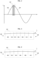
- Figure 2 is a waveform of the resonant current I L flowing through the resonant circuit LC
- Figure 3 is an enlarged view of a portion of the waveform of Figure 2 during an independent laser activation phase
- Figure 4 is an enlarged view of a portion of the waveform of Figure 2 during a sequential laser activation phase.
- the high-side and low-side switches S2_j and S3_j are driven by the control circuit 18 in half-bridge configuration so that: when the high-side switch S2_j is on (i.e., closed, conductive), the corresponding low-side switch S3_j is off (open, nonconductive), and the corresponding laser diode LD_j can be activated by injecting current in the latter through the respective light-emission channel; and, when the high-side switch S2_j is off, the low-side switch S3_j is on, thus coupling the respective driving node 13_j to the reference node GND and countering undesired spurious currents that could flow through the laser diode LD_j. It will otherwise be noted that provision of the low-side switches S3_j may not be essential for the operation of the laser lighting module 11, so that one or more embodiments may not be provided with low-side switches S3_j and the corresponding driving circuitry.
- control switches S1 and S1_0 are initially off, so that the capacitor Cr is charged by the regulator 16 to a voltage value (e.g., comprised between approximately 10 V and approximately 20 V) that is adequate for obtaining a desired current in the resonant circuit LC (e.g., comprised between approximately 20 A and approximately 60 A).
- the control switches S1 and S1_0 are then both switched on, so that the resonant circuit LC starts to oscillate and the current I L increases in the inductor Lr (see, e.g., the waveform portion 250 in Figure 2 ), with the resonant current being distributed (e.g., shared, split) between switches S1 and S1_0.
- a laser firing phase starts (see, e.g., the waveform portion 252 in Figure 2 , which is enlarged in Figures 3 and 4 ).
- the control switch S1 is turned off while the control switch S1_0 remains on, so that the resonant current I L is forced to flow through switch S1_0 only.
- the control switch S1 will remain off for the entire duration of the firing phase 252.
- the control switch S1_0 is also turned off while one of the high-side switches S2_j is turned on, so that the resonant current I L flowing through the inductor Lr is deviated in the respective laser diode LD_j and light emission takes place for the desired pulse duration (e.g., 1 ns).
- the control switch S1_0 is again turned on while the high-side switch S2_j previously activated is turned off, so that the resonant current I L is again forced to flow through switch S1_0 only.
- Portions 306 and 310 of the firing phase 252 substantially reproduce the behavior of portion 302 (i.e., switch S1_0 is turned off and one of the high-side switches S2_j is turned on), while portions 308 and 312 of the firing phase 252 substantially reproduce the behavior of portions 300 and 304 (i.e., switch S1_0 is turned on and all the high-side switches S2_j are turned off).
- both control switches S1 and S1_0 are switched on again (see, e.g., the waveform portion 254 in Figure 2 ).
- the control switch S1 is turned off while the control switch S1_0 remains on, so that the resonant current I L is forced to flow through switch S1_0 only.
- the control switch S1 will remain off for the entire duration of the firing phase 252.
- the control switch S1_0 is also turned off while the high-side switch S2_1 is turned on, so that the resonant current I L flowing through the inductor Lr is deviated in the laser diode LD_1 and light emission takes place for the desired pulse duration (e.g., 1 ns).
- the control switch S1_0 remains off, the high-side switch S2_1is turned off, and the subsequent high-side switch S2_2 is turned on, so that the resonant current I L is deviated in the laser diode LD_2.
- the control switch S1_0 remains off, the high-side switch S2_2 is turned off, and the subsequent high-side switch S2_3 is turned on, so that the resonant current I L is deviated in the laser diode LD_3.
- the control switch S1_0 remains off, the high-side switch S2_3 is turned off, and the subsequent high-side switch S2_4 is turned on, so that the resonant current I L is deviated in the laser diode LD_4.
- control switch S1_0 is again turned on while the high-side switch S2_4 (as well as the other high-side switches) is turned off, so that the resonant current I L is again forced to flow through switch S1_0 only.
- both control switches S1 and S1_0 are switched on again (see, e.g., the waveform portion 254 in Figure 2 ) .
- laser firing is obtained by switching the control switch S1_0 off and on so that when switch S1_0 is off, one of the high-side switches S2_j is on and vice-versa.
- Switch S1 instead remains off for the entire duration of the laser firing phase.
- the entirety of the resonant current stored in the resonant circuit LC (Lr, Cr) is transferred to switch S1_0 before the laser firing phase.
- Switch S1_0 is switched on and off to transfer the current I L in the laser diodes.
- Switch S1 is switched on again at the end of the laser firing phase.
- control switches S1 and S1_0 may be dimensioned differently so as to improve the performance of the driver circuit 100, insofar as they play a different function in the operation of the laser lighting module 11.
- switch S1 may be larger than switch S1_0. Therefore, switch S1 may have an on-state resistance (R DS,on ) lower than the on-state resistance of switch S1_0, at the price of a higher output capacitance (e.g., switch S1 having an output capacitance being about twice the output capacitance of switch S1_0, such as 180 pF for switch S1 and 90 pF for switch S1_0).
- one or more embodiments facilitate reducing power dissipation, switching time and current overshoot.
- the power dissipation in switch S1_0 may also be reduced since its short conduction time (e.g., ns range) minimizes the RMS current flowing through switch S1_0.
- the switching performance during current transfer to the laser diodes LD_j is improved insofar as the commutation is driven (only) by switch S1_0 that has an output capacitance smaller than switch S1.
- Such a smaller output capacitance combined with a reduction of stray inductances obtained by shortening the conduction path of the commutation loop, minimizes the resonant period and the current overshoot during commutation of switch S1_0.
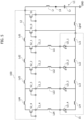
- FIG. 5 is a circuit diagram that illustrates certain components of the laser lighting module 11.
- the driver circuit 100 the laser diodes LD_j and the resonant circuit coupled to each other, and some parasitic inductances that may be present.
- parasitic inductances Ld1, Ld2, Ld3, Ld4 e.g., having an inductance of about 50 pH each
- inductance Ld1 may be located between the drain terminals of transistors S2_1and S1_0
- inductance Ld2 may be located between the drain terminals of transistors S2_2 and S2_1
- inductance Ld3 may be located between the drain terminals of transistors S2_3 and S2_2
- inductance Ld4 may be located between the drain terminals of transistors S2_4 and S2_3.
- parasitic inductances Ls1, Ls2, Ls3, Ls4 may be present at the source terminals of the high-side GaN transistors S2_1, S2_2, S2_3, S2_4, respectively; in particular, inductance Ls1 may be located between the source terminal of transistor S2_1 and the anode terminal of laser diode LD_1; inductance Ls2 may be located between the source terminal of transistor S2_2 and the anode terminal of laser diode LD_2; inductance Ls3 may be located between the source terminal of transistor S2_3 and the anode terminal of laser diode LD_3; inductance Ls4 may be located between the source terminal of transistor S2_4 and the anode terminal of laser diode LD_4.
- inductance Ls1 may be located between the source terminal of transistor S2_1 and the anode terminal of laser diode LD_1
- inductance Ls2 may be located between the source terminal of transistor S2_2 and the
- parasitic inductances Lc1 e.g., having an inductance of about 100 pH
- Lc2, Lc3, Lc4 e.g., having an inductance of about 50 pH each
- inductance Lc1 may be located between the cathode terminal of laser diode S2_1 and the source terminal of GaN transistor S1_0
- inductance Lc2 may be located between the cathode terminals of laser diodes LD_2 and LD_1
- inductance Lc3 may be located between the cathode terminals of laser diodes LD_3 and LD_2
- inductance Lc4 may be located between the cathode terminals of laser diodes LD_4 and LD_3.
- parasitic inductance Lgnd (e.g., having an inductance of about 1 nH) may be located between the source terminals of transistors S1_0 and S1. Additionally, transistor S1_0 may have an output capacitance of about 90 pF and transistor S1 may have an output capacitance of about 180 pF.
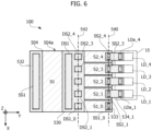
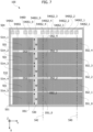
- Figures 6 and 7 are layout diagrams that exemplify the chip layout (e.g., in a top view) of a GaN integrated circuit 100 according to one or more embodiments.
- the integrated circuit 100 includes a semiconductor body 504 (of semiconductor material such as gallium nitride, GaN).
- the semiconductor body 504 has a first (e.g., top or upper) surface 504a and a second (e.g., bottom or lower) surface 504b parallel to plane XY and opposite to one another along an axis Z (e.g., axis Z being orthogonal to the plane of the sheet of Figures 6 and 7 , which is plane XY).
- the semiconductor body 504 includes the control switches S1 and S1_0, as well as the high-side switches S2_j (in this example, four switches S2_1, S2_2, S2_3 and S2_4).
- some parts of the integrated circuit 100 are not shown in Figures 6 and 7 and will not be discussed in the following (e.g., gate terminals and metallizations, possible passivation layers, etc.).
- the source terminal of the control switch S1 is designated by reference SS1
- the source terminal of the control switch S1_0 is designated by reference SS1_0
- the source terminals of the high-side switches S2_j are designated by references SS2_j.
- the drain terminal of the control switch S1 is designated by reference DS1
- the drain terminal of the control switch S1_0 is designated by reference DS1_0
- the drain terminals of the high-side switches S2_j are designated by references DS2_j.
- the source terminal SS1 of the control switch S1 is electrically connected via conductive vias that extend along direction Z and a source metallization 532 (e.g., including metal such as copper and/or gold) to a reference conductive layer (hereinafter referred to as layer GND, and for example including metal such as copper and/or gold), which extends in the semiconductor body 504.
- a source metallization 532 e.g., including metal such as copper and/or gold
- layer GND reference conductive layer
- a drain metallization 530 extends on the drains DS1, DS1_0 and DS2_j of the control switches S1, S1_0 and of the high-side switches S2_j, electrically contacting together these drains DS1, DS1_0 and DS2_j and operating as node 12 (common drain).
- the drain metallization 530 is electrically connected via further conductive vias to a conductive drain layer (e.g., including metal such as copper and/or gold) that extends in the semiconductor body 504, for example underneath the layer GND 506.
- the source terminal SS1_0 of the control switch S1_0 is electrically connected via conductive vias that extend along direction Z to a respective source metallization 533 (e.g., including metal such as copper and/or gold).
- the source terminals SS2_j of the high-side switches S2_j are electrically connected via conductive vias that extend along direction Z to respective source metallizations 534_j (e.g., including metal such as copper and/or gold).
- the source metallization 532 extends on the source terminal SS1 of the control switch S1 so as to set, also through conductive vias, the source terminal SS1 in electrical contact with the layer GND 506.
- each source metallization 534_j extends on the source terminal SS2_j of a respective high-side switch S2_j so as to set, also through conductive vias, the respective source terminal SS2_j in electrical contact with a respective output pin/pad of the integrated circuit 100, which can be used for coupling to the anode terminal LDa_j of a respective laser diode LD_j once the laser lighting module 11 is assembled.
- the common drain metallization 530 extends on the drain terminals DS1, DS1_0 and DS2_j of the control switches and of the high-side switches S2_j so as to set, also through conductive vias, all drain terminals in electrical contact with a respective output pin/pad of the integrated circuit 100, which can be used for coupling to the supply line 12 once the laser lighting module 11 is assembled.
- the source terminal SS1 of the control switch S1 and the source terminal SS1_0 of the control switch S1_0 may not be connected inside the package of the laser-driving device 101 (e.g., a SiP).
- the device 101 may be provided with dedicated pads for terminals SS1 and SS1_0, and these pads can be electrically connected outside the package of device 101 (e.g., using vias towards the ground layer of a printed circuit board where the cathode terminals of the laser diodes LD_j are soldered as well).
- gate metallizations and gate connections are not visible in Figures 6 and 7 for the sake of ease of illustration.
- I/O pads designated in Figure 7 by the following references: 540G1 indicating the pad for the gate terminal of the control switch S1, 540S1 indicating the pad for the source terminal SS1 of the control switch S1, 540D indicating the pad for the common drain terminal of the control switches and high-side switches, 540S1_0 indicating the pad for the source terminal SS1_0 of the control switch S1_0, 540G1_0 indicating the pad for the gate terminal of the control switch S1_0, 540S2_j indicating the pad for the source terminal SS2_j of a respective high-side switch S2_j, and 540G2_j indicating the pad for the gate terminal of a respective high-side switch S2_j.
- the source terminals SS2_j are located in a position corresponding to a lateral surface of the semiconductor body 504, which joins together the first and second surfaces (parallel to plane XY and opposite along direction Z) of the semiconductor body 504, optionally at the top of the lateral surface of the semiconductor body 504. For instance, they face the (top) surface of the semiconductor body 504 at an edge of the latter that extends between the (top) surface and the lateral surface.
- the source terminals SS2_j of the high-side switches S2_j as well as the source terminal SS1_0 of the control switch S1_0 are aligned with one another in a direction of alignment 540 parallel to the axis X
- the drains DS2_j of the high-side switches S2_j as well as the drain terminal DS1_0 of the control switch S1_0 are aligned with one another in a direction of alignment 542 parallel to the axis X.
- the source terminal SS1 and the drain terminal DS1 of the control switch S1 are aligned with one another in a respective direction perpendicular to the directions of alignment 540 and 542, and therefore parallel to the axis Y.
- the control switch S1 has its respective drain terminal DS1 facing the drain terminals DS2_j and DS1_0 of the high-side switches S2_j and of the control switch S1_0, so as to simplify mutual electrical coupling of the latter by the drain metallization 530.
- the conductive channels of switches S1, S1_0 and S2_j may thus all extend (e.g., in a plane parallel to the first surface 504a of the semiconductor body 504) in the same direction, which is perpendicular to the direction of alignment 540, with the source terminal SS1 of the first control switch S1 being located at an opposite side of the semiconductor body 504 with respect to the source terminals SS1_0 and SS2_j of the second control switch S1_0 and of the high-side switches S2_j .
- the high-side switches S2_j have an area of extension, in the plane XY defined by the axes X and Y, that is designed on the basis of the RMS currents and/or the peak current that are to flow in the respective laser diodes LD_j.
- the area of extension of each high-side switch S2_j is such that a density of RMS current generated thereby is approximately 20 A/mm 2 (value measured at approximately 25°C) and, optionally, the respective on-state resistance RDSon is approximately 15 m ⁇ .
- control switch S1 may be implemented as a set of transistors connected in parallel.
- switch S1 may comprise a number of transistors equal to the number of high-side transistors S2_j plus the other control transistor S1_0 (e.g., five transistors in the example considered herein, indicated by references S1m_1, S1m_2, S1m_3, S1m_4, and S1m_5, cumulatively also referred to as S1m_k).
- the transistors S1m_k, the high-side transistors S2_j and the transistor S1_0 may all have the same channel width W, e.g., equal to 500 ⁇ m.
- the transistors S1m_k may have a channel length of about 858 ⁇ m.
- the high-side transistors S2_j as well as the transistor S1_0 may have the same channel length of about 1857 ⁇ m.
- the semiconductor chip 100 may have a total dimension (in the XY plane) of about 3200 ⁇ m measured along the X direction and 3104 ⁇ m measured along the Y direction.
- the high-side switches S2_j may be coupled to another integrated circuit 15 that includes the laser diodes LD_j.
- the integrated circuit 15 may consist of another semiconductor body, and the first surface 504a of semiconductor body 504 may face the surface of such another second semiconductor body.
- the solid body is formed by a printed circuit board (PCB) that includes one or more conductive paths (e.g., including metal such as copper), which extend on a first surface.
- the laser diodes LD_j when coupled to the solid body, extend on the first surface and are in electrical contact with one of the aforesaid conductive paths, which electrically contacts also the conductive vias and operates as reference node GND.
- a further conductive path between said conductive paths electrically contacts the drain metallization 530 and operates as first node or line 12.
- Also electrically coupled (for example, soldered on the first surface) to the solid body are the control circuit 18, the low-side switches S3_j, the resonant circuit LC and the regulator 16.
- Figure 8 is a time diagram exemplary of the switching behavior of a laser lighting module 11 according to one or more embodiments.
- the four waveforms of the individual currents flowing through the four laser diodes LD_j during a laser firing phase (e.g., see again phase 252 of Figure 2 ), which may be characterized by a rise time of about 380 ps and a current overshoot limited to about 5 A with respect to a target current of about 40 A.
- Figure 9 is an example of possible use of the laser lighting module 11 (more in particular, of the laser-driving device 101) in a LIDAR application.
- Figure 9 shows a vehicle V (e.g., an automobile) comprising the LIDAR apparatus 1.
- the LIDAR apparatus 1 defines an emitter path EP and a receiver path RP.
- the emitter path EP includes the laser lighting module 11, in turn including the laser diodes (here designated by LD) and the laser-driving device 101 that operates as driving system for the laser diodes LD, as discussed previously.
- the emitter path EP also includes a LIDAR mirror module 1002 (e.g., a MEMS mirror module), which receives actuation signals A from, and supplies sensing signals S to, a mirror driver (e.g., an ASIC) 1003, for instance with the capacity of lighting a surrounding environment with a vertical laser beam and carrying out in a horizontal direction a scan as desired in order to detect, in a reliable way, a pedestrian within a distance of a few meters.
- a LIDAR mirror module 1002 e.g., a MEMS mirror module
- a mirror driver e.g., an ASIC
- the receiver path RP includes a photodiode module 1004 sensitive to the reflected signal produced as a result of a reflection of the radiation emitted by the emitter path EP on objects lit up by said radiation, and a receiver circuit 1005 coupled to the photodiode module 1004.
- the LIDAR apparatus 1 further includes a controller 1006 (e.g., a multi-core microcontroller architecture, possibly including dedicated FPGA/LIDAR hardware accelerators 1006A) configured to: emit signals for triggering and setting the power of the TPS laser to the laser-driving device 101 for laser lighting; exchange driving information DI with the mirror driver 1003 of the mirror module 1002; and receive raw data RD from, and send information of trigger and gain setting TGS to, the receiver circuit 1005 coupled to the photodiode module 1004.
- a controller 1006 e.g., a multi-core microcontroller architecture, possibly including dedicated FPGA/LIDAR hardware accelerators 1006A
- emit signals for triggering and setting the power of the TPS laser to the laser-driving device 101 for laser lighting
- exchange driving information DI with the mirror driver 1003 of the mirror module 1002
- the architecture illustrated in Figure 9 is conventional in the art, which renders a more detailed description thereof superfluous. This applies, for example, with reference to the co-ordination of operation of the LIDAR apparatus 1 with operation of the vehicle V (for example, in view of the configuration data received in the controller 1006 and of cloud information of status points as issued by the controller 1006) .
Landscapes
- Physics & Mathematics (AREA)
- Engineering & Computer Science (AREA)
- General Physics & Mathematics (AREA)
- Electromagnetism (AREA)
- Computer Networks & Wireless Communication (AREA)
- Radar, Positioning & Navigation (AREA)
- Remote Sensing (AREA)
- Condensed Matter Physics & Semiconductors (AREA)
- Optics & Photonics (AREA)
- Semiconductor Lasers (AREA)
Abstract
Description
- The present disclosure relates to a driver circuit for LIDAR (Light Detection And Ranging or Laser Imaging Detection And Ranging) applications. In particular, it relates to a driver circuit couplable to a control circuit and to a plurality of laser diodes, for biasing them. In addition, the present disclosure relates to a laser-driving device (e.g., implemented as a System-in-Package, SiP) including the driver circuit and the control circuit, to a lighting module including the laser-driving device and the laser diodes, to a LIDAR apparatus including the lighting module, and to methods of operating the laser-driving device and the laser lighting module.
- Thanks to their 3D sensing capacity and to the ability to function in the dark and in unfavorable meteorological conditions, LIDAR systems are increasingly used in the automotive sector, in possible combination with video cameras and radar systems, for environmental mapping and for other safety applications, such as emergency braking, detection of pedestrians and collision avoidance.
- Very short high-current pulses (such as current pulses that have an intensity in the range of tens of amps with rise and fall times in the (sub) nanosecond time range, for example, of the order of 100 ps) are desirable for laser diodes for LIDAR systems used for measuring the distances with time-of-flight (ToF) measurements techniques with medium-to-short distance values (e.g., distances of less than approximately 100 m with resolution of measurement of about ±15 cm).
- Arrays of laser diodes including laser diodes activated in sequence or in parallel are also used for improving the signal-to-noise (S/N) ratio of the return signal received. Multi-channel drivers offer the possibility of selecting the diode (diodes) to be activated with a short current pulse of high intensity.
- Circuits, devices, lighting modules and apparatuses for use in LIDAR applications are known, for instance, from references
US 2022/0013982 A1 andUS 2022/0014187 A1 , which are assigned to the same Applicants of the instant application. Additionally, referencesUS 2022/0013984 A1 andUS 2021/0218223 A1 , which are also assigned to the same Applicants of the instant application, disclose implementation details of such circuits and devices. All the patent applications listed above are hereby incorporated herein by reference in their entireties, also for the purpose of possibly seeking protection for one or more of the features disclosed therein, which may contribute to solve the technical problem solved by one or more embodiments of the present disclosure. - However, existing LIDAR systems present non-negligible parasitic inductances (e.g., higher than 1 nH) and/or capacitances, in particular on account of the use of the arrays of laser diodes, which cause degraded electrical performance of the latter. For instance, known solutions may be limited by a current rating in the range of about 20 A, mainly due to the maximum current capability of the laser-selecting switches and the maximum power dissipation of the switch that is used to drive a resonant current wave. Attaining a higher current rating by increasing the chip size would result in: lengthier connections to ground (which result in increased stray inductances in the commutation loop), increased output capacitance of the switch that drives the resonant current wave, deteriorated switching time and increased current overshoot due to resonance in the commutation loop with a period in the nanosecond range (which result in a poor current control in the nanosecond range).
- Reduction of the parasitic inductances and/or capacitances is therefore a desirable feature in the implementation of a driver circuit for laser diodes designed for high current ratings.
- An object of one or more embodiments is to contribute in providing driver circuits having an improved topology and/or chip layout that results in reduced parasitic inductances and/or capacitances.
- According to one or more embodiments, such an object can be achieved by a driver circuit having the features set forth in the claims that follow.
- One or more embodiments may relate to a corresponding laser-driving device including a driver circuit and a control circuit.
- One or more embodiments may relate to a corresponding laser lighting module including a laser-driving device, one or more laser diodes and a power supply arrangement.
- One or more embodiments may relate to a corresponding LIDAR apparatus including a laser lighting module.
- One or more embodiments may relate to corresponding methods of operating the laser-driving device and the laser lighting module.
- The claims are an integral part of the technical teaching provided herein in respect of the embodiments.
- According to a first aspect of the present description, a driver circuit is couplable to a plurality of laser diodes. The driver circuit includes a semiconductor body having a first surface. The driver circuit includes a first control switch (e.g., transistor) having a drain terminal electrically coupled to a drain metallization and having a source terminal electrically coupled to a first source metallization. The drain metallization is configured to be electrically coupled to a power supply line and the first source metallization is configured to be coupled to cathode terminals of the laser diodes and to a reference node. The driver circuit includes a second control switch (e.g., transistor) having a drain terminal electrically coupled to the drain metallization and having a source terminal electrically coupled to a second source metallization. The second source metallization is configured to be coupled to the cathode terminals of the laser diodes and to a reference node. The driver circuit includes a plurality of high-side switches (e.g., transistors), each high-side switch having a respective drain terminal electrically coupled to the drain metallization and having a respective source terminal electrically coupled to a respective third source metallization. Each third source metallization is coupled to a respective drive output node for driving an anode terminal of a respective laser diode of the plurality of laser diodes. The drain metallization, the first source metallization, the second source metallization and the third source metallizations face the first surface of the semiconductor body, which is also configured to face the laser diodes. The second source metallization and the third source metallizations are aligned with one another in a direction of alignment and are superimposed, orthogonally to the direction of alignment, to the respective source terminals of the second control switch and of the high-side switches.
- One or more embodiments may thus provide a driver circuit for laser diodes having improved topology and layout that reduce parasitic inductances.
- According to another aspect of the present description, a laser-driving device (e.g., in the form of a System-in-Package, SiP) includes a driver circuit according to one or more embodiments and a control circuit for driving the first control switch, the second control switch and the high-side switches to cyclically generate pulses for activating the laser diodes. The control circuit is configured to:
- sense a voltage across a capacitor of an external resonant circuit;
- in response to the sensed voltage reaching a first threshold value, close the first control switch and the second control switch, thereby enabling the resonant circuit to oscillate with a current (e.g., increasing current) that flows in an inductor of the resonant circuit and is split between the first control switch and the second control switch;
- in response to the current flowing in the inductor of the resonant circuit reaching a second threshold value, open the first control switch and keep closed the second control switch for a first time interval, whereby the current flows entirely through the second control switch;
- in response to expiration of the first time interval, open the second control switch and close a first selected high-side switch for a second time interval, whereby the current flows entirely through the first selected high-side switch and is output via a respective first drive output node; and
- in response to expiration of the second time interval, open the first selected high-side switch.
- According to another aspect of the present description, a laser lighting module includes a laser-driving device according to one or more embodiments and a resonant circuit including an inductor and a capacitor having an intermediate node between them. The resonant circuit is coupled between the power supply line and the reference node. The laser lighting module further includes a charging circuitry coupled between a supply node and the intermediate node of the resonant circuit for charging the capacitor of the resonant circuit, and a plurality of laser diodes. Each of the laser diodes has an anode terminal electrically coupled to a respective one of the drive output nodes and a cathode terminal electrically coupled to the reference node.
- According to another aspect of the present description, a LIDAR apparatus includes a laser light emitter path including a LIDAR mirror module and a laser lighting module according to one or more embodiments, a laser light receiver path including a photodiode module and a receiver circuit coupled to the photodiode module, and a controller circuit. The controller circuit is configured to emit driving signals for the LIDAR mirror module and the laser lighting module, and receive raw data from the receiver circuit coupled to the photodiode module.
- According to another aspect of the present description, a method of operating a laser-driving device according to one or more embodiments includes:
- sensing a voltage across a capacitor of an external resonant circuit;
- in response to the sensed voltage reaching a first threshold value, closing the first control switch and the second control switch, thereby enabling the resonant circuit to oscillate with a current that flows in an inductor of the resonant circuit and is split between the first control switch and the second control switch;
- in response to the current flowing in the inductor of the resonant circuit reaching a second threshold value, opening the first control switch and keeping closed the second control switch for a first time interval, whereby the current flows entirely through the second control switch;
- in response to expiration of the first time interval, opening the second control switch and closing a first selected high-side switch for a second time interval, whereby the current flows entirely through the first selected high-side switch and is output via a respective first drive output node; and
- in response to expiration of the second time interval, opening the first selected high-side switch.
- According to another aspect of the present description, a method of operating a laser lighting module according to one or more embodiments includes:
- initially opening the first control switch and the second control switch to charge the capacitor via the charging circuitry, and
- operating the laser-driving device according to the method of one or more embodiments.
- One or more embodiments will now be described, by way of example only, with reference to the annexed figures, wherein:
-
Figure 1 is a circuit diagram exemplary of a laser lighting module that may be included in a LIDAR apparatus according to one or more embodiments of the present description; -
Figures 2, 3 and 4 are waveforms exemplary of the resonant current flowing through a resonant circuit according to one or more embodiments of the present description; -
Figure 5 is a circuit diagram exemplary of certain components of a laser lighting module according to one or more embodiments of the present description; -
Figures 6 and7 are circuit layout diagrams exemplary of the chip layout of a driver circuit according to one or more embodiments of the present description; -
Figure 8 is a time diagram exemplary of the switching behavior of a laser lighting module according to one or more embodiments of the present description; and -
Figure 9 is a circuit block diagram exemplary of a LIDAR apparatus, possibly mounted on a vehicle, according to one or more embodiments of the present description. - In the ensuing description, one or more specific details are illustrated, aimed at providing an in-depth understanding of examples of embodiments of this description. The embodiments may be obtained without one or more of the specific details, or with other methods, components, materials, etc. In other cases, known structures, materials, or operations are not illustrated or described in detail so that certain aspects of embodiments will not be obscured.
- Reference to "an embodiment" or "one embodiment" in the framework of the present description is intended to indicate that a particular configuration, structure, or characteristic described in relation to the embodiment is included in at least one embodiment. Hence, phrases such as "in an embodiment" or "in one embodiment" that may be present in one or more points of the present description do not necessarily refer to one and the same embodiment. Moreover, particular configurations, structures, or characteristics may be combined in any adequate way in one or more embodiments.
- The headings/references used herein are provided merely for convenience and hence do not define the extent of protection or the scope of the embodiments.
- Throughout the figures annexed herein, unless the context indicates otherwise, like parts or elements are indicated with like references/numerals and a corresponding description will not be repeated for the sake of brevity.
-
Figure 1 is a circuit diagram exemplary of alaser lighting module 11 that may be included in a LIDAR apparatus 1 (exemplified inFigure 9 ), according to an embodiment of the present disclosure. - The
laser lighting module 11 includes a laser-driving device and a plurality of laser diodes. For instance, inFigure 1 four laser diodes are illustrated, which are arranged in an array and are designated by the reference symbols LD_1, LD_2, LD_3, LD_4 (generally LD_j, where j = 1, 2, ..., n and n is the number of laser diodes that form the array; by way of non-limiting example, thus, n = 4). The laser diodes LD_j are configured to be selectively activated (e.g., in a pulsed way) by respective half-bridge circuits. In particular, each half-bridge circuit includes a pair of electronic switches such as field-effect transistors and, for example, HEMT (High Electron Mobility Transistor) devices and/or MOSFET (Metal-Oxide-Semiconductor Field-Effect Transistor) devices. In detail, each half-bridge circuit includes a high-side switch S2_j (e.g., S2_1, S2_2, S2_3, S2_4 in the example ofFigure 1 ) coupled between apower supply line 12 common to all the half-bridge circuits and a respective driving node 13_j (e.g., 13_1, 13_2, 13_3, 13_4 in the example ofFigure 1 ), and a low-side switch S3_j (e.g., S3_1, S3_2, S3_3, S3_4 in the example ofFigure 1 ) coupled between the respective driving node 13_j and a reference line (e.g., a ground GND, referred to in what follows as reference node GND) common to all the half-bridge circuits. The cathode terminal of each laser diode LD_j is coupled to the reference node GND, and the anode terminal of each laser diode LD_j is coupled to the driving node 13_j of the respective half-bridge circuit (e.g., the laser diodes LD_j are arranged in a common-cathode configuration). Thus, a first half-bridge S2_1, S3_1 drives a first laser diode LD_1, a second half-bridge S2_2, S3_2 drives a second laser diode LD_2, a third half-bridge S2_3, S3_3 drives a third laser diode LD_3, and a fourth half-bridge S2_4, S3_4 drives a fourth laser diode LD_4. The half-bridge circuits are driven byrespective driving circuits 10j coupled to the control terminals (e.g., gate terminals) of the high-side switches S2_j and low-side switches S3_j. - A resonant tank (or circuit) LC that includes an inductor Lr and a capacitor Cr connected in series is coupled between the
power supply line 12 and the reference node GND. The inductor Lr is arranged between thepower supply line 12 and anintermediate node 14 of the resonant circuit LC, and the capacitor Cr is arranged between theintermediate node 14 and the reference node GND. Theintermediate node 14 is coupled to a charge circuit (also referred to in what follows as regulator) 16, of a known type, which receives a supply voltage VCC. - A first control switch S1, such as a gallium nitride (GaN) field-effect transistor (for example, a GaN HEMT), is coupled between the
power supply line 12 and the reference node GND. A second control switch S1_0, such as a gallium nitride (GaN) field-effect transistor (for example, a GaN HEMT), is also coupled between thepower supply line 12 and the reference node GND. The control switches S1, S1_0 and the half-bridge switches S2_j, S3_j are driven as a function of enable signals supplied, as discussed hereinafter, by a control circuit designated as a whole byreference numeral 18, which includes the half-bridge driving circuits 10j. It may be considered that thecontrol circuit 18 includes: the half-bridge driving circuits 10j;respective control circuits 182j for the half-bridge driving circuits 10j configured to send to the half-bridge driving circuits 10j respective enable signals Ton_S2_j to enable supply of energy to (and therefore emission of light from) the respective laser diodes LD_j; acontrol circuit 201 configured to control the first control switch S1 (e.g., driving its control terminal, i.e., a gate terminal in the case of a field-effect transistor); and acontrol circuit 202 configured to control the second control switch S1_0 (e.g., driving its control terminal, i.e., a gate terminal in the case of a field-effect transistor). - As mentioned earlier, the
control circuits bridge driving circuits 10j, are represented as distinct entities purely for simplicity of description and understanding. These control and driving circuits may be integrated in asingle control unit 18, which may also incorporate the low-side switches S3_j. In fact, it will be understood that the components of alaser lighting module 11 as exemplified inFigure 1 may be arranged as follows: - the high-side switches S2_j and the control switches S1, S1_0, which may all be implemented as GaN power transistors (e.g., configured to operate in the power range of 100 W), may be (monolithically) integrated in a GaN integrated circuit (IC) 100, which may per se form an embodiment according to an aspect of the present disclosure (e.g., a driver circuit 100);
- the low-side switches S3_j and the control and driving
circuits GaN circuit 100 and theCMOS circuit 18 may be incorporated in a same package (e.g., as a System-in-Package, SiP, or as a single solid body of semiconductor material) and form an embodiment according to another aspect of the present disclosure (e.g., a laser-driving device 101); - the laser diodes LD_j may be provided as discrete components or incorporated in an
integrated circuit 15, and they may be coupled (e.g., by an end user such as a system integrator) to the laser-driving device 101 (e.g., being mounted on a printed circuit board, PCB, or being housed in a cavity of the solid body of semiconductor material) together with the resonant circuit LC and theregulator 16 to form an embodiment according to another aspect of the present disclosure (e.g., alaser lighting module 11 that may be used as a transmitter stage in aLIDAR apparatus 1 for distance measurement by time-of-flight, ToF, methods). - As described more comprehensively in the following, the
control circuit 18 enables co-ordination of operation of the control switches S1 and S1_0 with operation of the high-side switches S2_j and of the low-side switches S3_j in order to generate (ultra)short current pulses (e.g., having rise times and fall times in the order of the (sub)nanosecond time range and, for example, in the order of 100 ps), with high di/dt (e.g., higher than approximately 80 nA/ns) and high magnitude (e.g., reaching 40 A or more), which are switched on the laser diodes LD_j to obtain individual activation (e.g., sequential activation with a delay in the order of 1 ns) and selective emission of light. - In particular, the control switches S1 and S1_0 are connected in parallel to all the light-emission channels, as well as to the resonant circuit LC, and are thus configured to control energy supply from the
regulator 16 to the resonant circuit LC, thereby defining the energy content and the peak current of the pulses of the laser diodes LD_j when activated. Theregulator 16 can be implemented in a manner known per se so as to charge the capacitor Cr in the resonant circuit LC to a voltage adequate for obtaining a peak current in the resonant circuit LC equal to or higher than a desired pulse current of the laser diodes LD_j. - There now follows a description of a method of operating the
laser lighting module 11. Such a method may be better understood with reference toFigures 2, 3 and 4 , whereFigure 2 is a waveform of the resonant current IL flowing through the resonant circuit LC,Figure 3 is an enlarged view of a portion of the waveform ofFigure 2 during an independent laser activation phase, andFigure 4 is an enlarged view of a portion of the waveform ofFigure 2 during a sequential laser activation phase. - In particular, the high-side and low-side switches S2_j and S3_j are driven by the
control circuit 18 in half-bridge configuration so that: when the high-side switch S2_j is on (i.e., closed, conductive), the corresponding low-side switch S3_j is off (open, nonconductive), and the corresponding laser diode LD_j can be activated by injecting current in the latter through the respective light-emission channel; and, when the high-side switch S2_j is off, the low-side switch S3_j is on, thus coupling the respective driving node 13_j to the reference node GND and countering undesired spurious currents that could flow through the laser diode LD_j. It will otherwise be noted that provision of the low-side switches S3_j may not be essential for the operation of thelaser lighting module 11, so that one or more embodiments may not be provided with low-side switches S3_j and the corresponding driving circuitry. - In greater detail, the control switches S1 and S1_0 are initially off, so that the capacitor Cr is charged by the
regulator 16 to a voltage value (e.g., comprised between approximately 10 V and approximately 20 V) that is adequate for obtaining a desired current in the resonant circuit LC (e.g., comprised between approximately 20 A and approximately 60 A). The control switches S1 and S1_0 are then both switched on, so that the resonant circuit LC starts to oscillate and the current IL increases in the inductor Lr (see, e.g., thewaveform portion 250 inFigure 2 ), with the resonant current being distributed (e.g., shared, split) between switches S1 and S1_0. In response to the fact that the current IL of the resonant circuit LC reaches a threshold, a laser firing phase starts (see, e.g., thewaveform portion 252 inFigure 2 , which is enlarged inFigures 3 and 4 ). - If the laser channels are driven in an independent manner (i.e., with the possibility of activating the laser diodes LD_j in any order during the firing phase 252), as exemplified in
Figure 3 , during aninitial portion 300 of the firing phase 252 (e.g., 1 ns before the expected laser firing) the control switch S1 is turned off while the control switch S1_0 remains on, so that the resonant current IL is forced to flow through switch S1_0 only. The control switch S1 will remain off for the entire duration of thefiring phase 252. During asubsequent portion 302 of thefiring phase 252, the control switch S1_0 is also turned off while one of the high-side switches S2_j is turned on, so that the resonant current IL flowing through the inductor Lr is deviated in the respective laser diode LD_j and light emission takes place for the desired pulse duration (e.g., 1 ns). During asubsequent portion 304 of thefiring phase 252, the control switch S1_0 is again turned on while the high-side switch S2_j previously activated is turned off, so that the resonant current IL is again forced to flow through switch S1_0 only.Portions firing phase 252 substantially reproduce the behavior of portion 302 (i.e., switch S1_0 is turned off and one of the high-side switches S2_j is turned on), whileportions firing phase 252 substantially reproduce the behavior ofportions 300 and 304 (i.e., switch S1_0 is turned on and all the high-side switches S2_j are turned off). At the end of thelaser firing phase 252, both control switches S1 and S1_0 are switched on again (see, e.g., thewaveform portion 254 inFigure 2 ). - According to a different driving scheme, if the laser channels are driven in a sequential manner (i.e., activating all the laser diodes LD_j sequentially), as exemplified in
Figure 4 , during aninitial portion 400 of the firing phase 252 (e.g., 1 ns before the expected laser firing) the control switch S1 is turned off while the control switch S1_0 remains on, so that the resonant current IL is forced to flow through switch S1_0 only. The control switch S1 will remain off for the entire duration of thefiring phase 252. During asubsequent portion 402 of thefiring phase 252, the control switch S1_0 is also turned off while the high-side switch S2_1 is turned on, so that the resonant current IL flowing through the inductor Lr is deviated in the laser diode LD_1 and light emission takes place for the desired pulse duration (e.g., 1 ns). During asubsequent portion 404 of thefiring phase 252, the control switch S1_0 remains off, the high-side switch S2_1is turned off, and the subsequent high-side switch S2_2 is turned on, so that the resonant current IL is deviated in the laser diode LD_2. During asubsequent portion 406 of thefiring phase 252, the control switch S1_0 remains off, the high-side switch S2_2 is turned off, and the subsequent high-side switch S2_3 is turned on, so that the resonant current IL is deviated in the laser diode LD_3. During asubsequent portion 408 of thefiring phase 252, the control switch S1_0 remains off, the high-side switch S2_3 is turned off, and the subsequent high-side switch S2_4 is turned on, so that the resonant current IL is deviated in the laser diode LD_4. During asubsequent portion 410 of thefiring phase 252, the control switch S1_0 is again turned on while the high-side switch S2_4 (as well as the other high-side switches) is turned off, so that the resonant current IL is again forced to flow through switch S1_0 only. At the end of thelaser firing phase 252, both control switches S1 and S1_0 are switched on again (see, e.g., thewaveform portion 254 inFigure 2 ) . - Therefore, in various embodiments, laser firing is obtained by switching the control switch S1_0 off and on so that when switch S1_0 is off, one of the high-side switches S2_j is on and vice-versa. Switch S1 instead remains off for the entire duration of the laser firing phase. The entirety of the resonant current stored in the resonant circuit LC (Lr, Cr) is transferred to switch S1_0 before the laser firing phase. Switch S1_0 is switched on and off to transfer the current IL in the laser diodes. Switch S1 is switched on again at the end of the laser firing phase.
- In various embodiments, the control switches S1 and S1_0 may be dimensioned differently so as to improve the performance of the
driver circuit 100, insofar as they play a different function in the operation of thelaser lighting module 11. In particular, switch S1 may be larger than switch S1_0. Therefore, switch S1 may have an on-state resistance (RDS,on) lower than the on-state resistance of switch S1_0, at the price of a higher output capacitance (e.g., switch S1 having an output capacitance being about twice the output capacitance of switch S1_0, such as 180 pF for switch S1 and 90 pF for switch S1_0). By doing so, one or more embodiments facilitate reducing power dissipation, switching time and current overshoot. In fact, the on-state resistance of switch S1 may be dimensioned to minimize the power dissipation while driving the resonant current IL in the inductor Lr (power = RDS,ON * IRMS), insofar as this dimensioning does not affect the switching time of the laser diodes since fast switching is performed by the other control switch S1_0. The power dissipation in switch S1_0 may also be reduced since its short conduction time (e.g., ns range) minimizes the RMS current flowing through switch S1_0. Thus, the switching performance during current transfer to the laser diodes LD_j is improved insofar as the commutation is driven (only) by switch S1_0 that has an output capacitance smaller than switch S1. Such a smaller output capacitance, combined with a reduction of stray inductances obtained by shortening the conduction path of the commutation loop, minimizes the resonant period and the current overshoot during commutation of switch S1_0. -
Figure 5 is a circuit diagram that illustrates certain components of thelaser lighting module 11. In particular, there are shown thedriver circuit 100, the laser diodes LD_j and the resonant circuit coupled to each other, and some parasitic inductances that may be present. For instance, parasitic inductances Ld1, Ld2, Ld3, Ld4 (e.g., having an inductance of about 50 pH each) may be present at the drain terminals of the high-side GaN transistors S2_1, S2_2, S2_3, S2_4, respectively; in particular, inductance Ld1 may be located between the drain terminals of transistors S2_1and S1_0; inductance Ld2 may be located between the drain terminals of transistors S2_2 and S2_1; inductance Ld3 may be located between the drain terminals of transistors S2_3 and S2_2; and inductance Ld4 may be located between the drain terminals of transistors S2_4 and S2_3. Additionally, parasitic inductances Ls1, Ls2, Ls3, Ls4 (e.g., having an inductance of about 25 pH each) may be present at the source terminals of the high-side GaN transistors S2_1, S2_2, S2_3, S2_4, respectively; in particular, inductance Ls1 may be located between the source terminal of transistor S2_1 and the anode terminal of laser diode LD_1; inductance Ls2 may be located between the source terminal of transistor S2_2 and the anode terminal of laser diode LD_2; inductance Ls3 may be located between the source terminal of transistor S2_3 and the anode terminal of laser diode LD_3; inductance Ls4 may be located between the source terminal of transistor S2_4 and the anode terminal of laser diode LD_4. Additionally, parasitic inductances Lc1 (e.g., having an inductance of about 100 pH) and Lc2, Lc3, Lc4 (e.g., having an inductance of about 50 pH each) may be present at the cathode terminals of the laser diodes LD_1, LD_2, LD_3, LD_4, respectively; in particular, inductance Lc1 may be located between the cathode terminal of laser diode S2_1 and the source terminal of GaN transistor S1_0; inductance Lc2 may be located between the cathode terminals of laser diodes LD_2 and LD_1; inductance Lc3 may be located between the cathode terminals of laser diodes LD_3 and LD_2; inductance Lc4 may be located between the cathode terminals of laser diodes LD_4 and LD_3. Additionally, parasitic inductance Lgnd (e.g., having an inductance of about 1 nH) may be located between the source terminals of transistors S1_0 and S1. Additionally, transistor S1_0 may have an output capacitance of about 90 pF and transistor S1 may have an output capacitance of about 180 pF. -
Figures 6 and7 are layout diagrams that exemplify the chip layout (e.g., in a top view) of a GaNintegrated circuit 100 according to one or more embodiments. - The
integrated circuit 100 includes a semiconductor body 504 (of semiconductor material such as gallium nitride, GaN). Thesemiconductor body 504 has a first (e.g., top or upper)surface 504a and a second (e.g., bottom or lower) surface 504b parallel to plane XY and opposite to one another along an axis Z (e.g., axis Z being orthogonal to the plane of the sheet ofFigures 6 and7 , which is plane XY). Thesemiconductor body 504 includes the control switches S1 and S1_0, as well as the high-side switches S2_j (in this example, four switches S2_1, S2_2, S2_3 and S2_4). For the sake of easy of illustration, some parts of theintegrated circuit 100 are not shown inFigures 6 and7 and will not be discussed in the following (e.g., gate terminals and metallizations, possible passivation layers, etc.). - In
Figures 6 and7 , the source terminal of the control switch S1 is designated by reference SS1, the source terminal of the control switch S1_0 is designated by reference SS1_0, and the source terminals of the high-side switches S2_j are designated by references SS2_j. Similarly, the drain terminal of the control switch S1 is designated by reference DS1, the drain terminal of the control switch S1_0 is designated by reference DS1_0, and the drain terminals of the high-side switches S2_j are designated by references DS2_j. - The source terminal SS1 of the control switch S1 is electrically connected via conductive vias that extend along direction Z and a source metallization 532 (e.g., including metal such as copper and/or gold) to a reference conductive layer (hereinafter referred to as layer GND, and for example including metal such as copper and/or gold), which extends in the
semiconductor body 504. Furthermore, a drain metallization 530 (e.g., a redistribution layer including metal such as copper and/or gold) extends on the drains DS1, DS1_0 and DS2_j of the control switches S1, S1_0 and of the high-side switches S2_j, electrically contacting together these drains DS1, DS1_0 and DS2_j and operating as node 12 (common drain). Thedrain metallization 530 is electrically connected via further conductive vias to a conductive drain layer (e.g., including metal such as copper and/or gold) that extends in thesemiconductor body 504, for example underneath the layer GND 506. Also, the source terminal SS1_0 of the control switch S1_0 is electrically connected via conductive vias that extend along direction Z to a respective source metallization 533 (e.g., including metal such as copper and/or gold). Additionally, the source terminals SS2_j of the high-side switches S2_j are electrically connected via conductive vias that extend along direction Z to respective source metallizations 534_j (e.g., including metal such as copper and/or gold). - Therefore, the
source metallization 532 extends on the source terminal SS1 of the control switch S1 so as to set, also through conductive vias, the source terminal SS1 in electrical contact with the layer GND 506. Moreover, each source metallization 534_j extends on the source terminal SS2_j of a respective high-side switch S2_j so as to set, also through conductive vias, the respective source terminal SS2_j in electrical contact with a respective output pin/pad of theintegrated circuit 100, which can be used for coupling to the anode terminal LDa_j of a respective laser diode LD_j once thelaser lighting module 11 is assembled. Moreover, thecommon drain metallization 530 extends on the drain terminals DS1, DS1_0 and DS2_j of the control switches and of the high-side switches S2_j so as to set, also through conductive vias, all drain terminals in electrical contact with a respective output pin/pad of theintegrated circuit 100, which can be used for coupling to thesupply line 12 once thelaser lighting module 11 is assembled. The source terminal SS1 of the control switch S1 and the source terminal SS1_0 of the control switch S1_0 may not be connected inside the package of the laser-driving device 101 (e.g., a SiP). Thedevice 101 may be provided with dedicated pads for terminals SS1 and SS1_0, and these pads can be electrically connected outside the package of device 101 (e.g., using vias towards the ground layer of a printed circuit board where the cathode terminals of the laser diodes LD_j are soldered as well). Again, it is noted that gate metallizations and gate connections are not visible inFigures 6 and7 for the sake of ease of illustration. - Optionally, electrical contact with the source, drain and/or gate terminals of the switches in the GaN
integrated circuit 100 are obtained by appropriate I/O pads, designated inFigure 7 by the following references: 540G1 indicating the pad for the gate terminal of the control switch S1, 540S1 indicating the pad for the source terminal SS1 of the control switch S1, 540D indicating the pad for the common drain terminal of the control switches and high-side switches, 540S1_0 indicating the pad for the source terminal SS1_0 of the control switch S1_0, 540G1_0 indicating the pad for the gate terminal of the control switch S1_0, 540S2_j indicating the pad for the source terminal SS2_j of a respective high-side switch S2_j, and 540G2_j indicating the pad for the gate terminal of a respective high-side switch S2_j. - Moreover, optionally, the source terminals SS2_j (and optionally also the source terminal SS1) are located in a position corresponding to a lateral surface of the
semiconductor body 504, which joins together the first and second surfaces (parallel to plane XY and opposite along direction Z) of thesemiconductor body 504, optionally at the top of the lateral surface of thesemiconductor body 504. For instance, they face the (top) surface of thesemiconductor body 504 at an edge of the latter that extends between the (top) surface and the lateral surface. - As exemplified in
Figures 6 and7 , the source terminals SS2_j of the high-side switches S2_j as well as the source terminal SS1_0 of the control switch S1_0 are aligned with one another in a direction ofalignment 540 parallel to the axis X, and the drains DS2_j of the high-side switches S2_j as well as the drain terminal DS1_0 of the control switch S1_0 are aligned with one another in a direction ofalignment 542 parallel to the axis X. In addition, the source terminal SS1 and the drain terminal DS1 of the control switch S1 are aligned with one another in a respective direction perpendicular to the directions ofalignment drain metallization 530. The conductive channels of switches S1, S1_0 and S2_j may thus all extend (e.g., in a plane parallel to thefirst surface 504a of the semiconductor body 504) in the same direction, which is perpendicular to the direction ofalignment 540, with the source terminal SS1 of the first control switch S1 being located at an opposite side of thesemiconductor body 504 with respect to the source terminals SS1_0 and SS2_j of the second control switch S1_0 and of the high-side switches S2_j . - Optionally, the high-side switches S2_j have an area of extension, in the plane XY defined by the axes X and Y, that is designed on the basis of the RMS currents and/or the peak current that are to flow in the respective laser diodes LD_j. For instance, the area of extension of each high-side switch S2_j is such that a density of RMS current generated thereby is approximately 20 A/mm2 (value measured at approximately 25°C) and, optionally, the respective on-state resistance RDSon is approximately 15 mΩ.
- As exemplified in
Figure 7 , the control switch S1 may be implemented as a set of transistors connected in parallel. In particular, switch S1 may comprise a number of transistors equal to the number of high-side transistors S2_j plus the other control transistor S1_0 (e.g., five transistors in the example considered herein, indicated by references S1m_1, S1m_2, S1m_3, S1m_4, and S1m_5, cumulatively also referred to as S1m_k). The transistors S1m_k, the high-side transistors S2_j and the transistor S1_0 may all have the same channel width W, e.g., equal to 500 µm. The transistors S1m_k may have a channel length of about 858 µm. The high-side transistors S2_j as well as the transistor S1_0 may have the same channel length of about 1857 µm. Thesemiconductor chip 100 may have a total dimension (in the XY plane) of about 3200 µm measured along the X direction and 3104 µm measured along the Y direction. - As previously discussed, the high-side switches S2_j may be coupled to another
integrated circuit 15 that includes the laser diodes LD_j. For instance, theintegrated circuit 15 may consist of another semiconductor body, and thefirst surface 504a ofsemiconductor body 504 may face the surface of such another second semiconductor body. - Furthermore, according to one or more embodiments the solid body is formed by a printed circuit board (PCB) that includes one or more conductive paths (e.g., including metal such as copper), which extend on a first surface. In this case, the laser diodes LD_j, when coupled to the solid body, extend on the first surface and are in electrical contact with one of the aforesaid conductive paths, which electrically contacts also the conductive vias and operates as reference node GND. Moreover, a further conductive path between said conductive paths electrically contacts the
drain metallization 530 and operates as first node orline 12. Also electrically coupled (for example, soldered on the first surface) to the solid body are thecontrol circuit 18, the low-side switches S3_j, the resonant circuit LC and theregulator 16. -
Figure 8 is a time diagram exemplary of the switching behavior of alaser lighting module 11 according to one or more embodiments. In particular, inFigure 8 are shown the four waveforms of the individual currents flowing through the four laser diodes LD_j during a laser firing phase (e.g., see againphase 252 ofFigure 2 ), which may be characterized by a rise time of about 380 ps and a current overshoot limited to about 5 A with respect to a target current of about 40 A. -
Figure 9 is an example of possible use of the laser lighting module 11 (more in particular, of the laser-driving device 101) in a LIDAR application. In particular,Figure 9 shows a vehicle V (e.g., an automobile) comprising theLIDAR apparatus 1. TheLIDAR apparatus 1 defines an emitter path EP and a receiver path RP. - The emitter path EP includes the
laser lighting module 11, in turn including the laser diodes (here designated by LD) and the laser-drivingdevice 101 that operates as driving system for the laser diodes LD, as discussed previously. The emitter path EP also includes a LIDAR mirror module 1002 (e.g., a MEMS mirror module), which receives actuation signals A from, and supplies sensing signals S to, a mirror driver (e.g., an ASIC) 1003, for instance with the capacity of lighting a surrounding environment with a vertical laser beam and carrying out in a horizontal direction a scan as desired in order to detect, in a reliable way, a pedestrian within a distance of a few meters. - The receiver path RP includes a
photodiode module 1004 sensitive to the reflected signal produced as a result of a reflection of the radiation emitted by the emitter path EP on objects lit up by said radiation, and areceiver circuit 1005 coupled to thephotodiode module 1004. - The
LIDAR apparatus 1 further includes a controller 1006 (e.g., a multi-core microcontroller architecture, possibly including dedicated FPGA/LIDAR hardware accelerators 1006A) configured to: emit signals for triggering and setting the power of the TPS laser to the laser-drivingdevice 101 for laser lighting; exchange driving information DI with themirror driver 1003 of themirror module 1002; and receive raw data RD from, and send information of trigger and gain setting TGS to, thereceiver circuit 1005 coupled to thephotodiode module 1004. - It may be noted that, except for the
laser lighting module 11 and more in particular the laser-drivingdevice 101, the architecture illustrated inFigure 9 is conventional in the art, which renders a more detailed description thereof superfluous. This applies, for example, with reference to the co-ordination of operation of theLIDAR apparatus 1 with operation of the vehicle V (for example, in view of the configuration data received in thecontroller 1006 and of cloud information of status points as issued by the controller 1006) . - Without prejudice to the underlying principles, the details and embodiments may vary, even significantly, with respect to what has been described by way of example only, without departing from the extent of protection.
- The extent of protection is determined by the annexed claims.
Claims (14)
- A driver circuit (100) couplable to a plurality of laser diodes (LD_j), the driver circuit (100) comprising:a semiconductor body (504) having a first surface (504a);a first control switch (S1) having a drain terminal (DS1) electrically coupled to a drain metallization (530) and having a source terminal (SS1) electrically coupled to a first source metallization (532), wherein the drain metallization (530) is configured to be electrically coupled to a power supply line (12) and the first source metallization (532) is configured to be coupled to cathode terminals of said laser diodes (LD_j) and to a reference node (GND);a second control switch (S1_0) having a drain terminal (DS1_0) electrically coupled to said drain metallization (530) and having a source terminal (SS1_0) electrically coupled to a second source metallization (533), wherein the second source metallization (533) is configured to be coupled to said cathode terminals of said laser diodes (LD_j) and to said reference node (GND) ;a plurality of high-side switches (S2_j), each high-side switch having a respective drain terminal (DS2_j) electrically coupled to said drain metallization (530) and having a respective source terminal (SS2_j) electrically coupled to a respective third source metallization (534_j), wherein each third source metallization (534_j) is coupled to a respective drive output node (13_j) for driving an anode terminal (LDa_j) of a respective laser diode (LD_j) of the plurality of laser diodes;wherein the drain metallization (530), the first source metallization (532), the second source metallization (533) and the third source metallizations (534_j) face the first surface (504a) of the semiconductor body (504), which is also configured to face the laser diodes (LD_j); andwherein the second source metallization (533) and the third source metallizations (534_j) are aligned with one another in a direction of alignment (540) and are superimposed, orthogonally to the direction of alignment (540), to the respective source terminals of the second control switch (S1_0) and of the high-side switches (S2_j).
- The driver circuit (100) of claim 1, wherein a conductive channel of said first control switch (S1) is larger than a conductive channel of said second control switch (S1_0), whereby an on-state resistance of said first control switch (S1) is smaller than an on-state resistance of said second control switch (S1_0).
- The driver circuit (100) of claim 1 or claim 2, wherein:said first control switch (S1), said second control switch (S1_0) and said high-side switches (S2_j) have respective conductive channels that extend in a direction perpendicular to said direction of alignment (540) and parallel to said first surface (540a); andsaid source terminal (SS1) of said first control switch (S1) is located at an opposite side of said semiconductor body (504) with respect to said source terminals (SS1_0, SS2_j) of said second control switch (S1_0) and of said high-side switches (S2_j).
- The driver circuit (100) of any of the previous claims, wherein said first control switch (S1) has a conductive channel having a width equal to the sum of the widths (W) of the conductive channels of said second control switch (S1_0) and of said high-side switches (S2_j).
- The driver circuit (100) of any of the previous claims, wherein said first control switch (S1) comprises a plurality of first control transistors (S1m_k) electrically connected in parallel, wherein preferably the number of said first control transistors (S1m_k) is equal to the number of said second control switch (S1_0) plus said high-side switches (S2_j).
- The driver circuit (100) of claim 5, wherein each of said first control transistors (S1m_k), each of said high-side switches (S2_j) and said second control switch (S1_0) have respective conductive channels having all the same width (W).
- A laser-driving device (101), comprising a driver circuit (100) according to any of the previous claims and a control circuit (18) for driving the first control switch (S1), the second control switch (S1_0) and the high-side switches (S2_j) to cyclically generate pulses for activating said laser diodes (LD_j), the control circuit (18) being configured to:sense a voltage across a capacitor (Cr) of an external resonant circuit (LC);in response to said sensed voltage reaching a first threshold value, close the first control switch (S1) and the second control switch (S1_0), thereby enabling the resonant circuit (LC) to oscillate with a current (IL) that flows in an inductor (Lr) of the resonant circuit (LC) and is split between the first control switch (S1) and the second control switch (S1_0);in response to said current (IL) flowing in the inductor (Lr) of the resonant circuit (LC) reaching a second threshold value, open the first control switch (S1) and keep closed the second control switch (S1_0) for a first time interval (300; 400), whereby said current (IL) flows entirely through said second control switch (S1_0);in response to expiration of said first time interval (300; 400), open the second control switch (S1_0) and close a first selected high-side switch (S2_1) for a second time interval (302; 402), whereby said current (IL) flows entirely through said first selected high-side switch (S2_1) and is output via a respective first drive output node (13_1); andin response to expiration of said second time interval (302; 402), open said first selected high-side switch (S2_1).
- The laser-driving device (101) of claim 7, wherein said control circuit (18) is further configured to:in response to expiration of said second time interval (302; 402), close a second selected high-side switch (S2_2) that is adjacent to said first selected high-side switch (S2_1) for a third time interval (404), whereby said current (IL) is switched from said first selected high-side switch (S2_1) to said second selected high-side switch (S2_2) and flows entirely through said second selected high-side switch (S2_2) and is output via a respective second drive output node (13_2); andin response to expiration of said third time interval (404), open said second selected high-side switch (S2_2).
- The laser-driving device (101) of claim 7, wherein said control circuit (18) is further configured to:in response to expiration of said second time interval (302; 402), close said second control switch (S1_0)for a third time interval (304), whereby said current (IL) is switched from said first selected high-side switch (S2_1) to said second control switch (S1_0) and flows entirely through said second control switch (S1_0); andin response to expiration of said third time interval (304), open said second control switch (S1_0) and close a second selected high-side switch (S2_j) for a fourth time interval (306), whereby said current (IL) flows entirely through said second selected high-side switch (S2_j) and is output via a respective second drive output node (13_j); andin response to expiration of said fourth time interval (306), open said second selected high-side switch (S2_j).
- The laser-driving device (101) of any of claims 7 to 9, wherein said control circuit (18) comprises a plurality of low-side switches (S3_j) configured for coupling to respective ones of said high-side switches (S2_j), wherein each low-side switch (S3_j) is configured to be coupled between a respective one of said drive output nodes (13_j) and said reference node (GND), and wherein said control circuit (18) is further configured to close each of said low-side switches (S3_j) when the respective high-side switch (S2_j) is open.
- A laser lighting module (11), comprising:a laser-driving device (101) according to any of claims 7 to 10;a resonant circuit (LC) including an inductor (Lr) and a capacitor (Cr) having an intermediate node (14) between them, the resonant circuit (LC) being coupled between the power supply line (12) and the reference node (GND);a charging circuitry (16) coupled between a supply node (VCC) and the intermediate node (14) of the resonant circuit (LC) for charging the capacitor (Cr) of the resonant circuit (LC); anda plurality of laser diodes (15, LD_j), wherein each of said laser diodes (LD_j) has an anode terminal (LDa_j) electrically coupled to a respective one of said drive output nodes (13_j) and a cathode terminal electrically coupled to said reference node (GND).
- A LIDAR apparatus (1), comprising:a laser light emitter path (EP) comprising a LIDAR mirror module (1002) and a laser lighting module (11) according to claim 11;a laser light receiver path (RP) comprising a photodiode module (1004) and a receiver circuit (1005) coupled to the photodiode module (1004); anda controller circuit (1006) configured to:emit driving signals (TPS, DI) for said LIDAR mirror module (1002) and said laser lighting module (11); andreceive raw data (RD) from said receiver circuit (1005) coupled to the photodiode module (1004).
- A method of operating a laser-driving device (101) according to any of claims 7 to 10, the method comprising:sensing a voltage across a capacitor (Cr) of an external resonant circuit (LC);in response to said sensed voltage reaching a first threshold value, closing the first control switch (S1) and the second control switch (S1_0), thereby enabling the resonant circuit (LC) to oscillate with a current (IL) that flows in an inductor (Lr) of the resonant circuit (LC) and is split between the first control switch (S1) and the second control switch (S1_0);in response to said current (IL) flowing in the inductor (Lr) of the resonant circuit (LC) reaching a second threshold value, opening the first control switch (S1) and keeping closed the second control switch (S1_0) for a first time interval (300; 400), whereby said current (IL) flows entirely through said second control switch (S1_0);in response to expiration of said first time interval (300; 400), opening the second control switch (S1_0) and closing a first selected high-side switch (S2_1) for a second time interval (302; 402), whereby said current (IL) flows entirely through said first selected high-side switch (S2_1) and is output via a respective first drive output node (13_1); andin response to expiration of said second time interval (302; 402), opening said first selected high-side switch (S2_1).
- A method of operating a laser lighting module (11) according to claim 11, the method comprising:initially opening the first control switch (S1) and the second control switch (S1_0) to charge said capacitor (Cr) via said charging circuitry (16), andoperating the laser-driving device (101) according to the method of claim 13.
Applications Claiming Priority (1)
| Application Number | Priority Date | Filing Date | Title |
|---|---|---|---|
| IT102022000025605A IT202200025605A1 (en) | 2022-12-14 | 2022-12-14 | Driver circuit, laser driver, laser illumination module, LIDAR apparatus and corresponding operating procedures |
Publications (2)
| Publication Number | Publication Date |
|---|---|
| EP4386437A1 true EP4386437A1 (en) | 2024-06-19 |
| EP4386437B1 EP4386437B1 (en) | 2025-05-14 |
Family
ID=85225070
Family Applications (1)
| Application Number | Title | Priority Date | Filing Date |
|---|---|---|---|
| EP23307132.3A Active EP4386437B1 (en) | 2022-12-14 | 2023-12-05 | Driver circuit, corresponding laser-driving device, laser lighting module, lidar apparatus and methods of operation |
Country Status (3)
| Country | Link |
|---|---|
| US (1) | US20240204478A1 (en) |
| EP (1) | EP4386437B1 (en) |
| IT (1) | IT202200025605A1 (en) |
Citations (6)
| Publication number | Priority date | Publication date | Assignee | Title |
|---|---|---|---|---|
| WO2019167039A1 (en) * | 2018-02-28 | 2019-09-06 | B. G. Negev Technologies And Applications Ltd., At Ben-Gurion University | Low voltage sub-nanosecond pulsed current driver ic for high-resolution lidar applications |
| US20210218223A1 (en) | 2019-12-20 | 2021-07-15 | Stmicroelectronics S.R.L. | Pulse generator circuit, related laser system and method |
| US20220013984A1 (en) | 2020-07-07 | 2022-01-13 | Stmicroelectronics (Rousset) Sas | Pulse generator circuit, related system and method |
| US20220014187A1 (en) | 2020-07-07 | 2022-01-13 | Stmicroelectronics (Rousset) Sas | Pulse generator circuit, related system and method |
| US20220013982A1 (en) | 2020-07-07 | 2022-01-13 | Stmicroelectronics S.R.L. | Electronic device for lidar applications |
| US20220149588A1 (en) * | 2020-03-25 | 2022-05-12 | Silanna Asia Pte Ltd | Pulsed laser diode driver |
-
2022
- 2022-12-14 IT IT102022000025605A patent/IT202200025605A1/en unknown
-
2023
- 2023-12-05 EP EP23307132.3A patent/EP4386437B1/en active Active
- 2023-12-08 US US18/533,585 patent/US20240204478A1/en active Pending
Patent Citations (6)
| Publication number | Priority date | Publication date | Assignee | Title |
|---|---|---|---|---|
| WO2019167039A1 (en) * | 2018-02-28 | 2019-09-06 | B. G. Negev Technologies And Applications Ltd., At Ben-Gurion University | Low voltage sub-nanosecond pulsed current driver ic for high-resolution lidar applications |
| US20210218223A1 (en) | 2019-12-20 | 2021-07-15 | Stmicroelectronics S.R.L. | Pulse generator circuit, related laser system and method |
| US20220149588A1 (en) * | 2020-03-25 | 2022-05-12 | Silanna Asia Pte Ltd | Pulsed laser diode driver |
| US20220013984A1 (en) | 2020-07-07 | 2022-01-13 | Stmicroelectronics (Rousset) Sas | Pulse generator circuit, related system and method |
| US20220014187A1 (en) | 2020-07-07 | 2022-01-13 | Stmicroelectronics (Rousset) Sas | Pulse generator circuit, related system and method |
| US20220013982A1 (en) | 2020-07-07 | 2022-01-13 | Stmicroelectronics S.R.L. | Electronic device for lidar applications |
Also Published As
| Publication number | Publication date |
|---|---|
| EP4386437B1 (en) | 2025-05-14 |
| IT202200025605A1 (en) | 2024-06-14 |
| US20240204478A1 (en) | 2024-06-20 |
Similar Documents
| Publication | Publication Date | Title |
|---|---|---|
| CN112868148B (en) | Fast-Pulse, High-Current Laser Driver | |
| US20230275397A1 (en) | Pulsed laser diode driver | |
| US12316072B2 (en) | Pulse generator circuit, related system and method | |
| Glaser | High power nanosecond pulse laser driver using an GaN FET | |
| KR102423155B1 (en) | Manufacturing method of laser diode array device, laser light emitting circuit and measuring apparatus | |
| US20180278017A1 (en) | Circuit and method for driving a laser diode | |
| CN112731350A (en) | Scanning driving circuit and control method of laser radar | |
| US20230178961A1 (en) | Light source system | |
| CN216055673U (en) | Laser emission module and laser radar | |
| KR20220012816A (en) | Light source system | |
| CN217848622U (en) | Electronic device, laser drive module, laser illumination module, and laser radar apparatus | |
| US20220013982A1 (en) | Electronic device for lidar applications | |
| Liu et al. | High-frequency pulsed laser driver using complementary GaN HEMTs | |
| Glaser | Optimizing performance of a pulsed laser diode driver based on a GaN FET | |
| EP4386437B1 (en) | Driver circuit, corresponding laser-driving device, laser lighting module, lidar apparatus and methods of operation | |
| US20250337219A1 (en) | Electronic module for generating light pulses for lidar applications and method for manufacturing the electronic module | |
| WO2024134404A1 (en) | Die-level current resonant laser diode driver | |
| CN118198854A (en) | Driver circuit, LIDAR device, driving apparatus, lighting module, and method of operating the same | |
| US11990729B2 (en) | Shaping pulses using a multi-section optical load | |
| US12580365B2 (en) | Laser driver for driving VCSEL | |
| US20210389428A1 (en) | Light emitting device for lidar | |
| CN116540213A (en) | Narrow pulse transmitting circuit | |
| TW202147653A (en) | Light transmitting device for lidar | |
| US20200281070A1 (en) | High speed high power laser assembly with cavity | |
| CN119812934A (en) | Electronic circuits and laser scanners |
Legal Events
| Date | Code | Title | Description |
|---|---|---|---|
| PUAI | Public reference made under article 153(3) epc to a published international application that has entered the european phase |
Free format text: ORIGINAL CODE: 0009012 |
|
| STAA | Information on the status of an ep patent application or granted ep patent |
Free format text: STATUS: REQUEST FOR EXAMINATION WAS MADE |
|
| 17P | Request for examination filed |
Effective date: 20231205 |
|
| AK | Designated contracting states |
Kind code of ref document: A1 Designated state(s): AL AT BE BG CH CY CZ DE DK EE ES FI FR GB GR HR HU IE IS IT LI LT LU LV MC ME MK MT NL NO PL PT RO RS SE SI SK SM TR |
|
| GRAP | Despatch of communication of intention to grant a patent |
Free format text: ORIGINAL CODE: EPIDOSNIGR1 |
|
| STAA | Information on the status of an ep patent application or granted ep patent |
Free format text: STATUS: GRANT OF PATENT IS INTENDED |
|
| RIC1 | Information provided on ipc code assigned before grant |
Ipc: H01S 5/40 20060101ALI20250116BHEP Ipc: H01S 5/042 20060101ALI20250116BHEP Ipc: G01S 17/10 20200101ALI20250116BHEP Ipc: G01S 7/484 20060101ALI20250116BHEP Ipc: G01S 7/481 20060101AFI20250116BHEP |
|
| INTG | Intention to grant announced |
Effective date: 20250130 |
|
| GRAS | Grant fee paid |
Free format text: ORIGINAL CODE: EPIDOSNIGR3 |
|
| GRAA | (expected) grant |
Free format text: ORIGINAL CODE: 0009210 |
|
| STAA | Information on the status of an ep patent application or granted ep patent |
Free format text: STATUS: THE PATENT HAS BEEN GRANTED |
|
| AK | Designated contracting states |
Kind code of ref document: B1 Designated state(s): AL AT BE BG CH CY CZ DE DK EE ES FI FR GB GR HR HU IE IS IT LI LT LU LV MC ME MK MT NL NO PL PT RO RS SE SI SK SM TR |
|
| REG | Reference to a national code |
Ref country code: GB Ref legal event code: FG4D |
|
| REG | Reference to a national code |
Ref country code: CH Ref legal event code: EP |
|
| REG | Reference to a national code |
Ref country code: DE Ref legal event code: R096 Ref document number: 602023003513 Country of ref document: DE |
|
| REG | Reference to a national code |
Ref country code: IE Ref legal event code: FG4D |
|
| REG | Reference to a national code |
Ref country code: NL Ref legal event code: MP Effective date: 20250514 |
|
| PG25 | Lapsed in a contracting state [announced via postgrant information from national office to epo] |
Ref country code: PT Free format text: LAPSE BECAUSE OF FAILURE TO SUBMIT A TRANSLATION OF THE DESCRIPTION OR TO PAY THE FEE WITHIN THE PRESCRIBED TIME-LIMIT Effective date: 20250915 Ref country code: ES Free format text: LAPSE BECAUSE OF FAILURE TO SUBMIT A TRANSLATION OF THE DESCRIPTION OR TO PAY THE FEE WITHIN THE PRESCRIBED TIME-LIMIT Effective date: 20250514 Ref country code: FI Free format text: LAPSE BECAUSE OF FAILURE TO SUBMIT A TRANSLATION OF THE DESCRIPTION OR TO PAY THE FEE WITHIN THE PRESCRIBED TIME-LIMIT Effective date: 20250514 |
|
| REG | Reference to a national code |
Ref country code: LT Ref legal event code: MG9D |
|
| PG25 | Lapsed in a contracting state [announced via postgrant information from national office to epo] |
Ref country code: NO Free format text: LAPSE BECAUSE OF FAILURE TO SUBMIT A TRANSLATION OF THE DESCRIPTION OR TO PAY THE FEE WITHIN THE PRESCRIBED TIME-LIMIT Effective date: 20250814 Ref country code: GR Free format text: LAPSE BECAUSE OF FAILURE TO SUBMIT A TRANSLATION OF THE DESCRIPTION OR TO PAY THE FEE WITHIN THE PRESCRIBED TIME-LIMIT Effective date: 20250815 |
|
| PG25 | Lapsed in a contracting state [announced via postgrant information from national office to epo] |
Ref country code: NL Free format text: LAPSE BECAUSE OF FAILURE TO SUBMIT A TRANSLATION OF THE DESCRIPTION OR TO PAY THE FEE WITHIN THE PRESCRIBED TIME-LIMIT Effective date: 20250514 Ref country code: PL Free format text: LAPSE BECAUSE OF FAILURE TO SUBMIT A TRANSLATION OF THE DESCRIPTION OR TO PAY THE FEE WITHIN THE PRESCRIBED TIME-LIMIT Effective date: 20250514 |
|
| REG | Reference to a national code |
Ref country code: AT Ref legal event code: MK05 Ref document number: 1795224 Country of ref document: AT Kind code of ref document: T Effective date: 20250514 |
|
| PG25 | Lapsed in a contracting state [announced via postgrant information from national office to epo] |
Ref country code: BG Free format text: LAPSE BECAUSE OF FAILURE TO SUBMIT A TRANSLATION OF THE DESCRIPTION OR TO PAY THE FEE WITHIN THE PRESCRIBED TIME-LIMIT Effective date: 20250514 |
|
| PG25 | Lapsed in a contracting state [announced via postgrant information from national office to epo] |
Ref country code: HR Free format text: LAPSE BECAUSE OF FAILURE TO SUBMIT A TRANSLATION OF THE DESCRIPTION OR TO PAY THE FEE WITHIN THE PRESCRIBED TIME-LIMIT Effective date: 20250514 |
|
| PG25 | Lapsed in a contracting state [announced via postgrant information from national office to epo] |
Ref country code: AT Free format text: LAPSE BECAUSE OF FAILURE TO SUBMIT A TRANSLATION OF THE DESCRIPTION OR TO PAY THE FEE WITHIN THE PRESCRIBED TIME-LIMIT Effective date: 20250514 |
|
| PG25 | Lapsed in a contracting state [announced via postgrant information from national office to epo] |
Ref country code: RS Free format text: LAPSE BECAUSE OF FAILURE TO SUBMIT A TRANSLATION OF THE DESCRIPTION OR TO PAY THE FEE WITHIN THE PRESCRIBED TIME-LIMIT Effective date: 20250814 |
|
| PG25 | Lapsed in a contracting state [announced via postgrant information from national office to epo] |
Ref country code: IS Free format text: LAPSE BECAUSE OF FAILURE TO SUBMIT A TRANSLATION OF THE DESCRIPTION OR TO PAY THE FEE WITHIN THE PRESCRIBED TIME-LIMIT Effective date: 20250914 |
|
| PG25 | Lapsed in a contracting state [announced via postgrant information from national office to epo] |
Ref country code: LV Free format text: LAPSE BECAUSE OF FAILURE TO SUBMIT A TRANSLATION OF THE DESCRIPTION OR TO PAY THE FEE WITHIN THE PRESCRIBED TIME-LIMIT Effective date: 20250514 |
|
| PG25 | Lapsed in a contracting state [announced via postgrant information from national office to epo] |
Ref country code: DK Free format text: LAPSE BECAUSE OF FAILURE TO SUBMIT A TRANSLATION OF THE DESCRIPTION OR TO PAY THE FEE WITHIN THE PRESCRIBED TIME-LIMIT Effective date: 20250514 Ref country code: SM Free format text: LAPSE BECAUSE OF FAILURE TO SUBMIT A TRANSLATION OF THE DESCRIPTION OR TO PAY THE FEE WITHIN THE PRESCRIBED TIME-LIMIT Effective date: 20250514 |
|
| PG25 | Lapsed in a contracting state [announced via postgrant information from national office to epo] |
Ref country code: CZ Free format text: LAPSE BECAUSE OF FAILURE TO SUBMIT A TRANSLATION OF THE DESCRIPTION OR TO PAY THE FEE WITHIN THE PRESCRIBED TIME-LIMIT Effective date: 20250514 |
|
| PG25 | Lapsed in a contracting state [announced via postgrant information from national office to epo] |
Ref country code: EE Free format text: LAPSE BECAUSE OF FAILURE TO SUBMIT A TRANSLATION OF THE DESCRIPTION OR TO PAY THE FEE WITHIN THE PRESCRIBED TIME-LIMIT Effective date: 20250514 |
|
| PG25 | Lapsed in a contracting state [announced via postgrant information from national office to epo] |
Ref country code: SK Free format text: LAPSE BECAUSE OF FAILURE TO SUBMIT A TRANSLATION OF THE DESCRIPTION OR TO PAY THE FEE WITHIN THE PRESCRIBED TIME-LIMIT Effective date: 20250514 |
|
| PG25 | Lapsed in a contracting state [announced via postgrant information from national office to epo] |
Ref country code: IT Free format text: LAPSE BECAUSE OF FAILURE TO SUBMIT A TRANSLATION OF THE DESCRIPTION OR TO PAY THE FEE WITHIN THE PRESCRIBED TIME-LIMIT Effective date: 20250514 |
|
| REG | Reference to a national code |
Ref country code: DE Ref legal event code: R097 Ref document number: 602023003513 Country of ref document: DE |
|
| PG25 | Lapsed in a contracting state [announced via postgrant information from national office to epo] |
Ref country code: RO Free format text: LAPSE BECAUSE OF FAILURE TO SUBMIT A TRANSLATION OF THE DESCRIPTION OR TO PAY THE FEE WITHIN THE PRESCRIBED TIME-LIMIT Effective date: 20250514 |
|
| PLBE | No opposition filed within time limit |
Free format text: ORIGINAL CODE: 0009261 |
|
| STAA | Information on the status of an ep patent application or granted ep patent |
Free format text: STATUS: NO OPPOSITION FILED WITHIN TIME LIMIT |
|
| REG | Reference to a national code |
Ref country code: CH Ref legal event code: L10 Free format text: ST27 STATUS EVENT CODE: U-0-0-L10-L00 (AS PROVIDED BY THE NATIONAL OFFICE) Effective date: 20260325 |
|
| 26N | No opposition filed |
Effective date: 20260217 |
|
| PG25 | Lapsed in a contracting state [announced via postgrant information from national office to epo] |
Ref country code: LT Free format text: LAPSE BECAUSE OF FAILURE TO SUBMIT A TRANSLATION OF THE DESCRIPTION OR TO PAY THE FEE WITHIN THE PRESCRIBED TIME-LIMIT Effective date: 20250514 |
|
| PG25 | Lapsed in a contracting state [announced via postgrant information from national office to epo] |
Ref country code: MC Free format text: LAPSE BECAUSE OF FAILURE TO SUBMIT A TRANSLATION OF THE DESCRIPTION OR TO PAY THE FEE WITHIN THE PRESCRIBED TIME-LIMIT Effective date: 20250514 |
|
| PGFP | Annual fee paid to national office [announced via postgrant information from national office to epo] |
Ref country code: DE Payment date: 20260421 Year of fee payment: 3 |
|
| PG25 | Lapsed in a contracting state [announced via postgrant information from national office to epo] |
Ref country code: SE Free format text: LAPSE BECAUSE OF FAILURE TO SUBMIT A TRANSLATION OF THE DESCRIPTION OR TO PAY THE FEE WITHIN THE PRESCRIBED TIME-LIMIT Effective date: 20250514 |