EP4383550A1 - Power conversion apparatus and control apparatus for same - Google Patents
Power conversion apparatus and control apparatus for same Download PDFInfo
- Publication number
- EP4383550A1 EP4383550A1 EP22853153.9A EP22853153A EP4383550A1 EP 4383550 A1 EP4383550 A1 EP 4383550A1 EP 22853153 A EP22853153 A EP 22853153A EP 4383550 A1 EP4383550 A1 EP 4383550A1
- Authority
- EP
- European Patent Office
- Prior art keywords
- converter
- power source
- power
- charging
- dsmmc
- Prior art date
- Legal status (The legal status is an assumption and is not a legal conclusion. Google has not performed a legal analysis and makes no representation as to the accuracy of the status listed.)
- Pending
Links
Images



Classifications
-
- H—ELECTRICITY
- H02—GENERATION; CONVERSION OR DISTRIBUTION OF ELECTRIC POWER
- H02M—APPARATUS FOR CONVERSION BETWEEN AC AND AC, BETWEEN AC AND DC, OR BETWEEN DC AND DC, AND FOR USE WITH MAINS OR SIMILAR POWER SUPPLY SYSTEMS; CONVERSION OF DC OR AC INPUT POWER INTO SURGE OUTPUT POWER; CONTROL OR REGULATION THEREOF
- H02M7/00—Conversion of AC power input into DC power output; Conversion of DC power input into AC power output
- H02M7/42—Conversion of DC power input into AC power output without possibility of reversal
- H02M7/44—Conversion of DC power input into AC power output without possibility of reversal by static converters
- H02M7/48—Conversion of DC power input into AC power output without possibility of reversal by static converters using discharge tubes with control electrode or semiconductor devices with control electrode
- H02M7/483—Converters with outputs that each can have more than two voltages levels
- H02M7/4835—Converters with outputs that each can have more than two voltages levels comprising two or more cells, each including a switchable capacitor, the capacitors having a nominal charge voltage which corresponds to a given fraction of the input voltage, and the capacitors being selectively connected in series to determine the instantaneous output voltage
-
- H—ELECTRICITY
- H02—GENERATION; CONVERSION OR DISTRIBUTION OF ELECTRIC POWER
- H02M—APPARATUS FOR CONVERSION BETWEEN AC AND AC, BETWEEN AC AND DC, OR BETWEEN DC AND DC, AND FOR USE WITH MAINS OR SIMILAR POWER SUPPLY SYSTEMS; CONVERSION OF DC OR AC INPUT POWER INTO SURGE OUTPUT POWER; CONTROL OR REGULATION THEREOF
- H02M1/00—Details of apparatus for conversion
- H02M1/32—Means for protecting converters other than automatic disconnection
- H02M1/322—Means for rapidly discharging a capacitor of the converter for protecting electrical components or for preventing electrical shock
-
- H—ELECTRICITY
- H02—GENERATION; CONVERSION OR DISTRIBUTION OF ELECTRIC POWER
- H02M—APPARATUS FOR CONVERSION BETWEEN AC AND AC, BETWEEN AC AND DC, OR BETWEEN DC AND DC, AND FOR USE WITH MAINS OR SIMILAR POWER SUPPLY SYSTEMS; CONVERSION OF DC OR AC INPUT POWER INTO SURGE OUTPUT POWER; CONTROL OR REGULATION THEREOF
- H02M1/00—Details of apparatus for conversion
- H02M1/36—Means for starting or stopping converters
-
- H—ELECTRICITY
- H02—GENERATION; CONVERSION OR DISTRIBUTION OF ELECTRIC POWER
- H02M—APPARATUS FOR CONVERSION BETWEEN AC AND AC, BETWEEN AC AND DC, OR BETWEEN DC AND DC, AND FOR USE WITH MAINS OR SIMILAR POWER SUPPLY SYSTEMS; CONVERSION OF DC OR AC INPUT POWER INTO SURGE OUTPUT POWER; CONTROL OR REGULATION THEREOF
- H02M1/00—Details of apparatus for conversion
- H02M1/0064—Magnetic structures combining different functions, e.g. storage, filtering or transformation
Definitions
- the present invention relates to a power conversion apparatus using a modular multilevel converter (hereinafter referred to as an MMC converter), and a control apparatus of the power conversion apparatus.
- MMC converter modular multilevel converter
- the MMC converter includes a voltage source such as a capacitor serving as an energy accumulation element, and a two-terminal arm converter configured by connecting multiple unit converters each constituted by a half-bridge circuit in series.
- the unit converter generates a desired voltage by controlling a PWM modulation factor of the half-bridge circuit.
- the capacitor serving as the energy accumulation element has the voltage fluctuated by repeating charging and discharging at the frequency determined by an output AC frequency of the MMC converter.
- the two-terminal arm converter connects a first terminal of the arm converter to a terminal of the AC power source at each phase, and a star connected second terminal to a terminal of a DC power source.
- the arm converter connected to each phase as described above generates a desired AC voltage to control the AC current, and simultaneously, superimposes the DC current for power conversion into/from the DC power source.
- the MMC converter executes the current control for adapting the arm current to an AC current command and a DC current command from the outside, implements the function for keeping the equilibrium of the average voltage of the capacitor among the unit converters by mutually adjusting the PWM modulation factors of the half-bridge circuits in the unit converters in an arm (hereinafter referred to as an interstage balance control), and implements the function for keeping the equilibrium of the total accumulated energy of the respective capacitors of the arm convertors (hereinafter referred to as a correlative balance control). Execution of the correlative balance control requires circuit elements for suppressing the circulating current between the arm converters.
- Patent Literature 1 discloses the means for providing the circulating current suppressing reactor between the first terminal of the arm convertor and the AC power source terminal for the purpose of suppressing the circulating current.
- Patent Literature 1 discloses the means in the form of an MMC converter of double star type (hereinafter referred to as a DSMMC converter).
- Non-Patent Literature 1 discloses that DC terminals of two DSMMC converters are connected behind to form the power conversion apparatus having one AC power source terminal connected to the power system, and the other AC power source terminal connected to the rotor. With respect to the means disclosed by Non-Patent Literature 1, the DC current is not superimposed on the rotor despite connection to the MMC converter. The means is adaptable to the case of making the speed of the rotor operated at a fixed frequency adjustable by direct connection to the power system.
- Patent Literature 2 discloses the initial charging device for charging the capacitor of the DSMMC converter.
- the DSMMC converter charges the capacitor from the initial charge power source upon initial starting.
- the capacitor is kept charged at high voltage. Accordingly, when stopping the converter, the capacitor charged at high voltage is preliminarily discharged to secure the safe state.
- Patent Literature 2 discloses the means for initially charging the capacitor while suppressing the rush current by connecting the initial charge resistance between initial charge power source and the DSMMC converter upon initial charging. Upon discharging, the DSMMC converter is operated in the state where the initial charge resistance and the three-phase short-circuit switch are combined to release energy accumulated in the capacitor by feeding the discharge current of the capacitor to the initial charge resistance.
- Non-Patent Literature 1 Makoto HAGIWARA, Kazutoshi NISHIMURA, Yasufumi AKAGI, "High-pressure motor drive using modular multilevel PWM inverter, First Report : Experimental Verification using miniature model at 400V, 15kw", Journal of IEEJ D, April 2010, Vol. 130, Num. 4, pp. 544-55
- the present invention relates to a power conversion apparatus constituted by a DSMMC converter, and a control apparatus of the power conversion apparatus. Problems to be considered and solved are described below.
- Patent Literature 2 does not disclose the means for initially charging and discharging two units of the DSMMC converters simultaneously. Accordingly, initial charging and discharging of the two DSMMC converters need time twice longer than the case of initial charging and discharging of the single DSMMC converter.
- the second problem is increase in size of the initial charging device.
- the size increase of the facility bottlenecks application of the device to the plant with limited installation area; and limited capacity, for example, the pumped storage power plant, and the offshore wind power plant.
- the size increase of the initial charging device results from necessity of increasing the size of the cooling device for initial charge resistance.
- the capacitor is charged and discharged via the initial charge resistance every time when performing initial charging and discharging operations of the DSMMC converter. Especially in the case of discharging, the initial charge resistance consumes entire energy accumulated in the capacitor. For the purpose of discharging in a short time, it is necessary to improve the discharging performance by increasing the size of the cooling device to avoid destruction owing to temperature rise of the resistance.
- the means is the means provided for regenerating energy accumulated in the capacitor into the AC power source associated with the DSMMC converter under the AC current control of the DSMMC converter so that the energy consumed by the resistance is reduced.
- the means is disadvantageous in that the regenerative operation range relies on the voltage VAC of the AC power source associated with the DSMMC converter. In other words, the regenerative operation range under the AC current control is limited up to the capacitor voltage VC at which the modulation factor M of the DSMMC converter does not reach the over-modulation operation region.
- the energy reduction amount of the initial charge resistance when applying the regenerative operation under the AC current control is calculated.
- the modulation factor M of the DSMMC converter is defined by the formula (1).
- the VAC denotes the line voltage effective value of the AC power source associated with the DSMMC converter
- k denotes the number of unit converters per arm converter
- VC denotes the capacitor voltage inside the unit converter
- C denotes the capacitance of the capacitor.
- the modulation factor during rated operation is set to be ranged from approximately 0.8 to 0.9. Assuming that values of VAC, k, and C in the formulae (1) and (2) are fixed, and the modulation factor during rated operation is 0.85, the modulation factor reaches the over-modulation operation region (M ⁇ 1.0) when the VC is lowered by approximately 17%. Compared with 100% energy consumption by the initial charge resistance as disclosed in Patent Literature 2 (entirely consumed by the resistance), the formula (2) provides approximately 70% energy consumption. There is a limit to energy reduction by approximately 30% at most, and accordingly, downsizing of the initial charging device by this means is restricted.
- the present invention provides a power conversion apparatus which includes a unit converter that is formed through parallel connection of a capacitor and a switching circuit constituted by two sets of series-connected switching elements having reflux diodes connected in parallel, a power converter that forms an arm having circulating current suppression reactors connected in series, forms a leg by two sets of the arms connected in series, and connects a connection point of the two sets of the arms, serving as an AC terminal to a phase of a first AC power source to cause both ends of the leg to serve as DC terminals, and a charging and discharging device having one end connected to a second AC power source, and the other end connected to the phase of the first AC power source.
- the charging and discharging device includes a tapped transformer which makes a position switchable between a high-voltage tap position and a low-voltage tap position, and is connected to the power converter instead of the first AC power source when starting and stopping the power converter.
- the present invention provides a control apparatus of a power conversion apparatus, which includes a unit converter that is formed through parallel connection of a capacitor and a switching circuit constituted by two sets of series-connected switching elements having reflux diodes connected in parallel, a power converter which forms an arm having circulating current suppression reactors connected in series, forms a leg by two sets of the arms connected in series, and connects a connection point of the two sets of the arms to a phase of a first AC power source to cause both ends of the leg to serve as DC terminals, and a charging and discharging device having one end connected to a second AC power source, and the other end connected to the phase of the first AC power source.
- the charging and discharging device includes a tapped transformer which makes a position switchable between a high-voltage tap position and a low-voltage tap position, and is connected to the power converter instead of the first AC power source when starting and stopping the power converter.
- the control apparatus makes a transition from a resistance charging mode to a bypass charging mode, and further to a switching charging mode for turn-on of the unit converter to connect the first AC power source instead of the second AC power source to the power converter.
- the second AC power source is connected to an AC terminal of the power converter via a resistance and the high-voltage tap position of the tapped transformer when starting the power converter.
- the bypass charging mode the AC terminal of the power converter is connected from the second AC power source via the tapped transformer.
- the present invention provides a control apparatus of a power conversion apparatus, which includes a unit converter that is formed through parallel connection of a capacitor and a switching circuit constituted by two sets of series-connected switching elements having reflux diodes connected in parallel, a power converter which forms an arm having circulating current suppression reactors connected in series, forms a leg by two sets of the arms connected in series, and connects a connection point of the two sets of the arms to a phase of a first AC power source to cause both ends of the leg to serve as DC terminals, and a charging and discharging device having one end connected to a second AC power source, and the other end connected to the phase of the first AC power source.
- the charging and discharging device includes a tapped transformer which makes a position switchable between a high-voltage tap position and a low-voltage tap position, and is connected to the power converter instead of the first AC power source when starting and stopping the power converter.
- the control apparatus makes a transition from a regenerative discharging mode to a resistance discharging mode.
- the second AC power source instead of the first AC power source is connected via the low-voltage tap position of the tapped transformer when stopping the power converter, and a gate pulse with a PWM modulation factor determined by a current control unit is given to the switching element to operate the power converter.
- the second AC power source is connected via the resistance from the low-voltage tap position of the tapped transformer to operate the power converter.
- the present invention allows simultaneous charging and discharging of all capacitors of the power conversion apparatus constituted by the DSMMC converter. This makes it possible to reduce the time for starting and stopping the power conversion apparatus.
- the initial charge transformer is tapped to allow selection of an AC power source voltage value which differs between operations of initial charging and discharging. Especially when discharging, the range of the regenerative operation into the initial charge power source can be expanded by lowering the AC. power source voltage value. It is therefore possible to significantly reduce energy to be consumed by the resistance. This makes it possible to provide the initial charging device which allows initial charging and discharging operations at high speeds without increasing size of the cooling device for heat dissipation of the resistance.
- a first embodiment describes an exemplary case of a main circuit structure of the power conversion apparatus according to the present invention.
- a second embodiment describes an exemplary case of a start control method of the power conversion apparatus which allows high-speed initial charging.
- a third embodiment describes an exemplary case of a stop control method of the power conversion apparatus which allows high-speed discharging.
- a fourth embodiment describes an exemplary case of a main circuit structure of the power conversion apparatus which is different from the first embodiment.
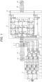
- FIG. 1 shows an embodiment of a main circuit structure of the power conversion apparatus according to a first embodiment of the present invention.
- the power conversion apparatus includes a power converter 1 (DSMMC converters 1A, 1B illustrated in the example), and an initial charging device 4.
- DSMMC converters 1A, 1B illustrated in the example DSMMC converters 1A, 1B illustrated in the example
- initial charging device 4 DSMMC converters 1A, 1B illustrated in the example
- DC terminals PA, PB and NA, NB of two sets of DSMMC converters 1A, 1B are connected behind, and AC terminals UA, VA, WA of the two sets of DSMMC converters 1A, 1B are connected to three-phase power sources 2A, 2B through main circuit breakers 6A, 6B, respectively so that power can be exchanged between the three-phase power sources 2A and 2B.
- the example represents that the above-described structure constitutes a frequency conversion system or a DC power transmission system.
- the present invention is applicable to the power conversion apparatus constituted by at least a set of the power converter 1 and the initial charging device 4.
- a voltage phase detection unit 3 calculates a voltage phase ⁇ from the three-phase AC voltage, and outputs the calculated result to a DSMMC controller 22.
- the initial charging device 4 as the other main component of the power conversion apparatus implements the function of charging the DSMMC converter 1A kept in a pre-start state, that is, internal capacitors kept in a non-charged state. When stopping the DSMMC converter 1A, the device implements the function of discharging the internal capacitors in a charged state.
- the initial charging device 4 may be regarded as the charging and discharging device.
- the initial charging device 4 as shown in FIG. 1 connects its terminals UP, VP, WP to lines having the respective AC terminals UA, VA, WA of the DSMMC converter 1A existing thereon. Terminals AA, BA, CA of the initial charging device 4 are connected to an initial charge power source 5.
- the DSMMC converter 1A is described as an example of the power converter 1. An explanation of the DSMMC converter 1B having the same structure as that of the DSMMC converter 1A is omitted.
- the DSMMC converter 1A includes six arm converters 17UP, 17UN, 17VP, 17VN, 17WP, 17WN, each of which has terminals A and B, six current detectors 18 each for detecting an arm current IUP, IUN, IVP, IVN, IWP, IWN at the respective phases, six circulating current suppression reactors 19, high resistances 20P, 20N, and current detectors 21P, 21N.
- the terminals A of the arm converters 17UP, 17VP, 17WP, and the terminals B of the arm converters 17UN, 17VN, 17WN are connected to the AC terminals UA, VA, WA via the current detectors 18 and the circulating current suppression reactors 19, respectively.
- the terminals B of the arm converters 17UP, 17VP, 17WP, and the terminals A of the arm converters 17UN, 17VN, 17WN are connected to the DC terminals PA, NA, and connected to DC terminals PB, NB of the other DSMMC converter 1B.
- the arm converter 17 has terminals C and D, which are connected to the DSMMC controller 22.
- connection relation of the DSMMC converter 1A may be simply explained in terms of a Graetz connection. That is, series circuits of the arm converters 17 and the circulating current suppression reactors 19 form an arm. A series circuit of two sets of arms forms a leg. Each connection point of the two sets of arms in the three sets of legs is connected to the respective phases of the AC power source. Both ends of each of three sets of legs are formed as DC terminals.
- the DC terminals PA, NA of the DSMMC converter 1A serve to fix the potential by grounding with the high resistances 20P, 20N so that a DC voltage VDC is subjected to the differential measurement by the current detectors 21P, 21N.
- the measured DC voltage VDC is transmitted to the DSMMC controller 22.
- the DSMMC controller 22 calculates a gate pulse g to be given to the respective unit converters based on input values of the arm currents IUP, IUN, IVP, IVN, IWP, IWN, the DC voltage VDC, the voltage phase ⁇ , the capacitor voltage VC of each unit converter, which has been obtained through the terminal D of the arm converter 17. The result is output to the terminal C of the respective arm converters 17.
- an explanation about the inner structure of the DSMMC converter 1B is omitted because of the same structure as that of the DSMMC converter 1A.
- the initial charging device 4 includes an initial charging device breaker 7, a three-phase short-circuit breaker 8, a discharge resistance 9, an initial charge resistance 10, a discharge breaker 11, an initial charge breaker 12, a resistance bypass breaker 13, a tapped initial charge transformer 14, and transformer tap switch breakers 15, 16.
- the initial charging device breaker 7 is an AC breaker for connecting the initial charging device 4 and the initial charge power source 5.
- the three-phase short-circuit breaker 8 is an AC breaker for star-connection of the discharge resistance 9 at each phase during a discharging operation.
- the discharge resistance 9 is a resistor for partially consuming energy accumulated in the capacitor during a discharging operation.
- the discharge breaker 11 is an AC breaker for connecting the discharge resistance 9 to the circuit during a discharging operation.
- the initial charge resistance 10 is a resistor for preventing the rush overcurrent during an initial charging operation.
- the initial charge breaker 12 is an AC breaker for connecting the initial charge resistance 10 to the circuit during an initial charging operation.
- the resistance bypass breaker 13 is an AC breaker for connection to the circuit without having the discharge resistance 9 or the initial charge resistance 10 intervened.
- the initial charging device 4 of the power conversion apparatus is characterized by the tapped initial charge transformer 14.
- the tap position differs between an initial charging operation for starting the power converter 1 and a discharging operation for stopping the power converter 1.
- the charging operation is performed at a full-voltage tap position (high-voltage tap position), and the discharging operation is performed at a half-voltage tap position (low-voltage tap position).
- the tapped initial charge transformer 14 is a transformer which includes first terminals AT, BT, CT at the side of theinitial charge power source 5 (hereinafter referred to as a primarywinding side), and includes second terminals UT1, VT1, WT1, and third terminals UT2, VT2, WT2 at the side of the DSMMC converter 1A (hereinafter referred to as a secondary winding side).
- the second terminals UT1, VT1, WT1, and the third terminals UT2, VT2, WT2 are provided so that each winding ratio to the primary winding becomes different.
- the above structure makes each AC voltage value of the respective terminals at the secondary winding side different.
- terminals are configured so that each AC voltage of the secondary winding of the second terminals UT1, VT1, WT1 is made higher than each AC voltage of the third terminals UT2, VT2, WT2.
- the second terminals UT1, VT1, WT1 are used during an initial charging operation.
- the third terminals UT2, VT2, and WT2 are used during a discharging operation.
- the transformer tap switch breakers 15, 16 are AC breakers for switching the connection terminal of the tapped initial charge transformer 14 at the secondary winding side.
- the transformer tap switch breaker 15 is switched to "close”, and the transformer tap switch breaker 16 is switched to "open” to connect the second terminals UT1, VT1, WT1 to the AC terminals UA, VA, WA of the DSMMC converter 1A, respectively.
- Those tap positions are so called full-tap positions (high-voltage tap positions).
- the transformer tap switch breaker 15 is switched to "open", and the transformer tap switch breaker 16 is switched to "close” to connect the third terminals UT2, VT2, WT2 to the AC terminals UA, VA, WA of the DSMMC converter 1A, respectively.
- Those tap positions are so called half-tap positions (low-voltage tap positions).
- the open/close condition of the respective breakers in the initial charging device 4 is switched in accordance with each operation mode to form a circuit for an initial charging operation and a circuit for a discharging operation.
- the first embodiment makes it possible to constitute the power conversion apparatus which satisfies the circuit structure and the condition adapted to the respective operations for charging and discharging the capacitor in the DSMMC converter 1.
- the tapped initial charge transformer 14 allows selection of the AC power source voltage value which differs between initial charging and discharging operations. Especially when discharging, the range of the regenerative operation into the initial charge power source can be expanded by lowering the AC power source voltage value. It is therefore possible to significantly reduce energy to be consumed by the resistance. This makes it possible to provide the initial charging device which allows initial charging and discharging operations at high speeds without increasing size of the cooling device for heat dissipation of the resistance.
- the second embodiment describes the method for start control of the power conversion apparatus that allows a high-speed initial charging operation.
- FIG. 2 shows an example of a circuit structure of the arm converter 17.
- An arm converter 17UP to be described herein has the structure similar to each structure of other arm converters 17UN, 17VP, 17VN, 17WP, 17WN. Accordingly, in this embodiment, explanations of other arm converters are omitted.
- the arm converter 17UP is a circuit formed by connecting k units of unit converters 23 in series.
- the term k denotes the number of unit converters 23 for each arm converter.
- the unit converter 23 is formed by connecting a switching circuit, a capacitor 25 as an energy accumulating element, and a voltage detector 26 for detecting an end-to-end voltage VC of the capacitor 25.
- the switching circuit is formed by connecting two switching elements 24H, 24L in series, each connected in parallel to a reflux diode.
- the unit converter 23 further includes two gate drive units (GDU) 28H, 28L for controlling the respective gates of the switching elements 24H, 24L.
- a signal converter (CONV) 29 outputs the end-to-end voltage VC of the capacitor 25, which has been detected by the voltage detector 26 to the DSMMC controller 22.
- the terminals A to D shown in FIG. 2 are input/output terminals of the arm converter 17UP, and correspond to the terminals A to D of the arm converter as shown in FIG. 1 .
- the terminal C is an input terminal which receives 2 ⁇ k gate pulses to be transmitted from the DSMMC controller 22 to the arm converter 17UP.
- the terminal D is an output terminal which transmits the end-to-end voltages VC of the k capacitors 25 from the arm converter 17UP to the DSMMC controller 22.
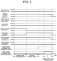
- FIG. 3 is a time chart indicating each open/close condition of the respective breakers in the initial charging device 4 as shown in FIG. 1 , and gate pulse output conditions of the DSMMC converters 1A, 1B during an initial charging operation.
- the three-phase short-circuit breaker 8 and the discharge breaker 11 are unrelated to the initial charging operation. As those breakers are kept “open” in the period from the time t0c to t4c during the initial charging operation, the explanation about the operation is omitted.
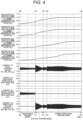
- FIG. 4 shows capacitor voltage waveforms of the DSMMC converters 1A, 1B during the initial charging operation, and AC current waveforms of the respective components in the initial charging device 4 according to the present invention.
- FIG. 4 shows the capacitor voltage of the arm converter 17UP of the DSMMC converter 1A, the capacitor voltage of the arm converter 17UN of the DSMMC converter 1A, the capacitor voltage of the arm converter 17UP of the DSMMC converter 1B, the capacitor voltage of the arm converter 17UN of the DSMMC converter 1B, currents IPA, IPB, IPC in the initial charging device 4, currents IRDA, IRDB, IRDC flowing to the discharge resistance 9, currents IRPA, IRPB, IRPC flowing to the initial charge resistance 10, and currents IBA, IBB, IBC flowing to the resistance bypass breaker 13 in the order from the top.
- the lateral axis denotes time t, and the time points t0c to t4c shown in FIG. 3 coincide with those shown in FIG. 4 .
- the capacitor voltage waveform represents only one voltage waveform of the capacitor of the representative unit converter in the arm converter 17UP or 17UN.
- the relationship among the AC currents is expressed as below.
- the main circuit breakers 6A, 6B are "open", and the three-phase power sources 2A, 2B and the DSMMC converters 1A, 1B are electrically disconnected.
- the initial charging device breaker 7 is "close”
- the initial charge breaker 12 is “close”
- the resistance bypass breaker 13 is “open”
- the transformer tap switch breakers 15 and 16 are "close” and "open”, respectively.
- the DSMMC converters 1A, 1B are connected to the initial charge power source 5 via the initial charge resistance 10 and the tapped initial charge transformer 14 in the initial charging device 4.
- the second terminals UT1, VT1, WT1 of the tapped initial charge transformer 14 at the secondary winding side are connected to the AC terminals UA, VA, WA of the DSMMC converter 1A.
- Each gate pulse output flag FLG_GDB of the DSMMC converters 1A, 1B is set to "0". Operations for switching the DSMMC converters 1A, 1B are stopped.
- the charging current is fed to the initial charge resistance 10 to charge the capacitors of the two DSMMC converters 1A, 1B via the initial charge resistance 10.
- the initial charge resistance 10 prevents the excessive rush current.
- the initial charge breaker 12 is switched from “close to open”, and the resistance bypass breaker 13 is switched from “open to close”.
- the initial charge resistance 10 is bypassed by the resistance bypass breaker 13 to charge the capacitors of the two DSMMC converters 1A, 1B.
- FIG. 4 shows, even if the initial charge resistance 10 is bypassed, it is possible to significantly suppress the rush current flowing into the initial charging device 4.
- the initial charging speed of the capacitor can be made higher than in the period from the time t0c to t1c in which charging is performed via the initial charge resistance 10.
- the rush current can be significantly restricted.
- the gate pulse output flag FLG_GDB of the DSMMC converter 1A is switched from “0 to 1" to start switching the DSMMC converter 1A.
- the gate pulse output flag FLG_GDB of the DSMMC converter 1B is switched from “0 to 1” to start switching the DSMMC converter 1B.
- the DSMMC converters 1A, 1B are switched to charge the respective capacitors of the DSMMC converters 1A, 1B until the target voltage value (1p. u.).
- the initial charging is completed.
- One of characteristics of the start control in the second embodiment is that a switching operation of a lower switching element 24L of the unit converter 23 shown in FIG. 2 is only started in the period from the time t2c to t4c. The switching operation of an upper switching element 24H of the unit converter 23 is kept stopped.
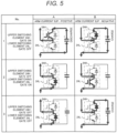
- a field A represents each state where the arm current IUP is positive
- a field B represents each state where the arm current IUP is negative.
- Nos. 1, 2, 3 represent gate ON/OFF states of the switching elements 24H, 24L. Definition of positive/negative current corresponds to the one shown in FIG. 1 .
- Each matrix defined by the lateral and the longitudinal axes represents the circuit structure of the unit converter 23, and the current path under the resultant condition in the charge/discharge state.
- the matrix No. 1-A indicates the discharging operation mode for discharging the capacitor
- the matrixes No. 1-B and No. 3-B indicate the charging operation mode for charging the capacitor
- other matrixes indicate the bypass operation mode in which current is not applied to the capacitor 25.
- the operation mode No. 1 for discharging the capacitor 25 is inadequate to the initial charging operation.
- the arm current IUP is positive in the inadequate mode
- the upper switching element 24H of the unit converter 23 is brought into a gate-on state
- the lower switching element 24L is brought into a gate-off state.
- the gate pulse output of the upper switching element 24H is stopped proactively to constantly keep the switching element off.
- the above-described control enables to always select the mode from four operation modes of Nos. 2 and 3 by omitting two operation modes of No. 1-A, No. 1-B as shown in FIG. 5 .
- the operation mode for discharging the capacitor 25 is not selected. This makes it possible to efficiently charge the capacitor. This is the reason for switching only the lower switching element 24L of the unit converter 23 in the period from the time t2c to t4c according to the present invention.
- FIG. 6 is a control block diagram for an initial charging operation of the DSMMC controller 22. Referring to the control block shown in FIG. 5 , the specific control method to be implemented in the period from the time t2c to t4c is described. Referring to FIG. 6 , the DSMMC controller 22 of the DSMMC converter 1A is described. In this embodiment, an explanation of the DSMMC controller 22 of the other DSMMC converter 1B is omitted because of the same control block structure.
- the DSMMC controller 22 shown in FIG. 6 includes a modulation factor determination unit 30, a PWM calculation unit 31, and a gate pulse output determination circuit 32.
- Gate pulses gHUP, gHVP, gHWP, gHUN, gHVN, gHWN as outputs as shown in FIG. 6 are given to the upper switching element 24H of the unit converter 23 shown in FIG. 2 .
- Gate pulses gLUP, gLVP, gLWP, gLUN, gLVN, gLWN are given to the lower switching element 24L of the unit converter 23.
- the gate pulse either "0" or "1" is output.
- the switching element is ON when the output is "1", and that the switching element is OFF when the output is "0".
- the gate pulse given to the upper switching element 24H during an initial charging operation is constantly OFF.
- the gate pulses gHUP, gHVP, gHWP, gHUN, gHVN, gHWN are always output as "0".
- the second characteristic of the start control in the second embodiment is that the modulation factor is controlled in the DSMMC switching charging mode, aiming at reduction in the time for starting.
- the modulation factor determination unit 30 as exemplified in FIG. 7 determines and outputs a modulated wave Mref given to the respective arm converters 17UP, 17UN, 17VP, 17VN, 17WP, 17WN of the DSMMC converter 1A in the period from the time t2c to t4c (DSMMC switching charging mode).
- the modulation factor determination unit 30 determines and outputs a modulated wave Mref given to the respective arm converters of the DSMMC converter 1B in the period from the time t3c to t4c.
- FIG. 7 shows an example of the modulated wave Mref at each time, which is output from the modulation factor determination unit 30.
- the modulation factor determination unit 30 of the DSMMC converter 1A at the time t2c outputs a modulated wave with the modulation factor Mref_A.
- the modulated wave is then compared with a carrier wave Carry to calculate gate pulses gLUP, gLVP, gLWP, gLUN, gLVN, gLWN.
- the modulation factor determination unit 30 of the DSMMC converter 1A at the time t4c outputs a modulated wave with the modulation factor Mref_B.
- the modulated wave is then compared with a carrier wave Carry to calculate gate pulses gLUP, gLVP, gLWP, gLUN, gLVN, gLWN.
- the modulated wave Mref is changed like a ramp in the operation period from the time t2c to t4c while changing an ON-OFF ratio of the lower switching element 24L. As FIG. 7 shows, the modulated wave Mref is changed with time to make the ratio between the charging operation mode and the bypass operation mode variable. This makes it possible to adjust the charging speed of the capacitor voltage of the DSMMC converter 1A.
- the DSMMC converter 1B is similarly operated except that the gate pulse output starting time is changed from t2c to t3c.
- the gate pulse output starting time of the DSMMC converter 1B is shifted to t3c from t2c of the DSMMC converter 1A to coincide the time taken to reach the target voltage value (1p. u.) by adjusting each charging speed of the respective capacitors.
- the PWM calculation unit 31 shown in FIG. 6 compares the modulated wave Mref calculated by the modulation factor determination unit 30 with the carrier wave Carry to output the gate pulse.
- the gate pulse output determination circuit 32 selects start/stop of the operation for switching the DSMMC converter 1A.
- the gate pulse output flag FLG_GDB is "0”
- the gate pulse output is constantly kept OFF to stop the switching operation.
- the gate pulse output flag FLG_GDB is "1”
- the gate pulse is output from the PWM calculation unit 31.
- the initial charging operation is completed by charging the capacitor until the target voltage value, switching the initial charging device breaker 7, the resistance bypass breaker 13, the transformer tap switch breaker 15 from “close to open”, and switching the gate pulse output flag FLG_GDB from "1 to 0" to electrically disconnect the DSMMC 1A, 1B from the initial charging device 4 at the time t4c when the voltage reaches the target voltage value.
- the second embodiment allows the charging to be performed in a short time.
- a third embodiment is described with respect to a stop control method of the power conversion apparatus that enables a high speed discharging.
- FIG. 8 is a time chart indicating each opening/closing of the.respective breakers in the initial charging device 4 as shown in FIG. 1 , and gate pulse output conditions of the DSMMC converters 1A, 1B during a discharging operation.
- the initial charge breaker 12 shown in FIG. 8 is unrelated to the discharging operation, and is kept “open” in the discharging operation period from the t0d to t3d as described below. Therefore, an explanation of the initial charge breaker 12 is omitted.
- FIG. 9 shows capacitor voltage waveforms of the DSMMC converters 1A, 1B during the discharging operation, and AC current waveforms of the respective components in the initial charging device 4 according to the present invention. Explanations of the respective waveforms shown in FIG. 9 are the same as those shown in FIG. 4 .
- the time points t0d to t3d shown in FIG. 8 coincide with those shown in FIG. 9 .
- the main circuit breakers 6A, 6B are switched from “close to open” for transition to the discharging operation mode to have regeneration into the initial charge power source 5 under the AC current control by the DSMMC converter.
- the three-phase power sources 2A, 2B, and the DSMMC converters 1A, 1B are electrically disconnected, respectively.
- the initial charging device breaker 7 is switched from “open to close”
- the three-phase short-circuit breaker 8 is switched to "open”
- the discharge breaker 11 is switched to "open”
- the resistance bypass breaker 13 is switched from “open to close”
- the transformer tap switch breaker 15 is switched to "open”
- the transformer tap switch breaker 16 is switched from "open to close”.
- the DSMMC converters 1A, 1B are then connected to the initial charge power source 5 via the tapped initial charge transformer 14 in the initial charging device 4.
- the third terminals UT2, VT2, WT2 of the tapped initial charge transformer 14 at the secondary winding side are connected to the AC terminals UA, VA, WA of the DSMMC converter 1A.
- Each of the gate pulse output flags FLG_GDB of the DSMMC converters 1A, 1B is switched from "0 to 1" so that the DSMMC converters 1A, 1B start switching operations.
- the power conversion apparatus With high voltage utilization rate. If the modulation factor during the rated operation is 0.85, the capacitor voltage is reduced by approximately 17%, resulting in an over-modulation operation. Thereafter, the regenerative operation into the power source cannot be performed. The energy of the capacitor is then inevitably consumed by the discharge resistance.
- the DSMMC converter can be operated until the capacitor voltage reaches 45% without causing over-modulation. As described referring to a first embodiment, this can be realized by switching the connection terminal of the tapped initial charge transformer 14 at the secondary winding side from the second,terminals UT1, VT1, WT1 to the third terminals UT2, VT2, WT2 to decrease the AC voltage value of the power source.
- the transformer tap switch breakers 15 and 16 are switched to "open” and “close”, respectively to connect the third terminals UT2, VT2, WT2 of the tapped initial charge transformer 14 at the secondary winding side to the AC terminals UA, VA, WA of the DSMMC converter 1A.
- the second terminals UT1, VT1, WT1, and the third terminals UT2, VT2, WT2 are provided so that winding ratio to the primary winding becomes different.
- the turn ratio with respect to the secondary winding is set so that each terminal voltage of the second terminals UT1, VT1, WT1 becomes twice higher than each terminal voltage of the third terminals UT2, VT2, WT2, respectively.
- the third terminals UT2, VT2, WT2 are connected during the discharging operation. This makes it possible to decrease the AC voltage value of the power source by appropriately half compared with connection to the second terminals UT1, VT1, WT1. As the AC voltage of the secondary winding of the tapped initial charge transformer 14 is reduced by approximately half, a margin of the modulation factor can be increased. This makes it possible to discharge the capacitor voltage up to 45%.
- the above-described structure allows regeneration of most part of energy accumulated in the capacitor into the power source.
- each gate pulse output flag FLG_GDB of the DSMMC converters 1A, 1B is switched from "1 to 0" to temporarily stop switching operations of the DSMMC converters 1A, 1B, and a preparatory step is taken for transition to the discharging operation mode using the discharge resistance 9.
- the initial charging device breaker 7 is switched from “close to open”
- the three-phase short-circuit breaker 8 is switched from “open to close”
- the discharge breaker 11 is switched from “open to close”
- the resistance bypass breaker 13 is switched from “close to open”.
- Each gate pulse output flag FLG_GDB of the DSMMC converters 1A, 1B is switched from “0 to 1” to resume the switching operations of the DSMMC converters 1A, 1B for transition to the discharging operation mode using the discharge resistance 9.
- the discharging mode is switched in the period from the time t1d to t2d.
- the discharging operation is performed by feeding current to the discharge resistance 9 under the AC current control of the DSMMC converter to allow consumption of energy accumulated in the capacitors of the DSMMC converters 1A, 1B.
- discharged capacitor voltage can be reduced to 45% from 100%.
- energy consumption by the discharge resistance 9 is 100% (energy is entirely consumed by the resistance) as disclosed in Patent Literature 2
- the energy consumption of the embodiment results in approximately 20% as expressed by the formula (2). This indicates that the energy to be consumed by the discharge resistance 9 can be reduced by approximately 80%. This may avoid size increase of the cooling device, and accordingly, it is possible to downsize the initial charging device.
- FIG. 10 is a control block diagram of the DSMMC controller 22 during the discharging operation. Referring to the control block shown in FIG. 10 , an explanation is concretely made about the specific method of controlling the DSMMC converter 1A in the period from the time t0d to t1d, and the period from the t2d to t3d. As the DSMMC converter 1B is operated with the constant modulation factor of 0.5 in the period from the time t0d to t1d, and the period from the time t2d to t3d, the explanation of the control method of the DSMMC converter 1B, thus is omitted.
- the DSMMC controller 22 in the stopped state as shown in FIG. 10 is constituted by an AC current calculation unit 33, a three-phase/two-phase conversion unit 34, an AC current control unit 35, a three-phase/two-phase inverse conversion unit 36, a Q-axis current command calculation unit 37, the PWM calculation unit 31, the gate pulse output determination circuit 32, and a dead time calculation unit 38.
- the PWM calculation unit 31 and the gate pulse output determination circuit 32 are similar to those operated during the initial charging operation, and accordingly, explanations of those components are omitted.
- the AC current calculation unit 33 obtains AC currents IU, IV, IW from arm currents IUP, IUN, IVP, IVN, IWP, IWN at the respective phases, which have been detected by the current detector 18 using the following formulae.
- IW IWP ⁇ IWN
- the three-phase/two-phase conversion unit 34 converts the three-phase AC currents IU, IV, IW into the Q-axis current IQ and the D-axis current ID.
- the relationship among the IU, IV, IW, the IQ, ID, and the voltage phase ⁇ is expressed by a formula (3).
- IQ ID 2 3 cos ⁇ cos ⁇ ⁇ 2 3 ⁇ cos ⁇ + 2 3 ⁇ sin ⁇ sin ⁇ ⁇ 2 3 ⁇ sin ⁇ + 2 3 ⁇ IU IV IW
- the AC current control unit 35 generates AC voltage commands VQref, VDref to cause the AC currents IQ, ID to follow AC current command values IQref, IDref.
- the AC current control unit 35 is constituted by a proportional integral controller.
- the three-phase/two-phase inverse conversion unit 36 converts VQref, VDref to the three-phase AC voltage commands VUref, VVref and VWref.
- the relationship among the IQ, ID, IU, the IV, IW, and the voltage phase ⁇ is expressed by a formula (4).
- IU IV IW cos ⁇ sin ⁇ cos ⁇ ⁇ 2 3 ⁇ sin ⁇ ⁇ 2 3 ⁇ cos ⁇ + 2 3 ⁇ sin ⁇ + 2 3 ⁇ IQ ID
- AC voltage commands VUParef, VVParef, VWParef, which are given to the arm converters 17UP, 17VP, 17WP, and AC voltage commands VUNaref, WNaref, VWNaref, which are given to the arm converters 17UN, 17VN, 17WN are generated from the VUref, VVref, Vwref.
- a DC voltage command VDCref/2 is added to the AC voltage command to calculate arm voltage commands VUPref, VUNref, VVPref, WNref, VWPref, VWNref.
- the dead time calculation unit 38 implements a function of preventing both the upper switching element 24H and the lower switching element 24L from being turned ON simultaneously by adding the dead time to the gate pulse derived from the PWM calculation unit 31.
- the Q-axis current command calculation unit 37 calculates the Q-axis current command IQref in accordance with the DC voltage VDC. Specifically, the IQref is set to satisfy the formula (5).
- the term R denotes a resistance value of the discharge resistance 9
- the term X denotes a leakage reactance, of the tapped initial charge transformer 14.
- the initial charging operation as described above allows simultaneous charging of the capacitor of the power conversion apparatus constituted by two units of the DSMMC converters while preventing the rush overcurrent during the initial charging operation. This makes it possible to reduce the time for starting and stopping the power conversion apparatus.
- the initial charge transformer 14 is tapped to implement the function for adjusting the power source voltage value by switching the tap of the transformer. Compared with the means disclosed in Patent Literature 2, the regenerative operation range during the discharging operation is expanded to reduce the energy consumed by the discharge resistance by approximately 80%.
- FIG. 11 shows an example of a main circuit structure of a power conversion apparatus according to a fourth embodiment of the present invention.
- FIG. 11 is different from FIG. 1 according to the first embodiment in that the initial charging device 4 does not include the discharge resistance 9 and the discharge breaker 11 therein.
- the initial charge resistance 10 serves to implement the function of the eliminated discharge resistance
- the initial charge breaker 12 serves to implement the function of the discharge breaker.
- the structure as shown in FIG. 11 allows further downsizing of the initial charging device.
Landscapes
- Engineering & Computer Science (AREA)
- Power Engineering (AREA)
- Rectifiers (AREA)
- Inverter Devices (AREA)
Abstract
Description
- The present invention relates to a power conversion apparatus using a modular multilevel converter (hereinafter referred to as an MMC converter), and a control apparatus of the power conversion apparatus.
- The MMC converter includes a voltage source such as a capacitor serving as an energy accumulation element, and a two-terminal arm converter configured by connecting multiple unit converters each constituted by a half-bridge circuit in series. The unit converter generates a desired voltage by controlling a PWM modulation factor of the half-bridge circuit. The capacitor serving as the energy accumulation element has the voltage fluctuated by repeating charging and discharging at the frequency determined by an output AC frequency of the MMC converter.
- The two-terminal arm converter connects a first terminal of the arm converter to a terminal of the AC power source at each phase, and a star connected second terminal to a terminal of a DC power source. The arm converter connected to each phase as described above generates a desired AC voltage to control the AC current, and simultaneously, superimposes the DC current for power conversion into/from the DC power source.
- The MMC converter executes the current control for adapting the arm current to an AC current command and a DC current command from the outside, implements the function for keeping the equilibrium of the average voltage of the capacitor among the unit converters by mutually adjusting the PWM modulation factors of the half-bridge circuits in the unit converters in an arm (hereinafter referred to as an interstage balance control), and implements the function for keeping the equilibrium of the total accumulated energy of the respective capacitors of the arm convertors (hereinafter referred to as a correlative balance control). Execution of the correlative balance control requires circuit elements for suppressing the circulating current between the arm converters.
-
Patent Literature 1 discloses the means for providing the circulating current suppressing reactor between the first terminal of the arm convertor and the AC power source terminal for the purpose of suppressing the circulating current.Patent Literature 1 discloses the means in the form of an MMC converter of double star type (hereinafter referred to as a DSMMC converter). - Non-Patent Literature 1 discloses that DC terminals of two DSMMC converters are connected behind to form the power conversion apparatus having one AC power source terminal connected to the power system, and the other AC power source terminal connected to the rotor. With respect to the means disclosed by Non-Patent
Literature 1, the DC current is not superimposed on the rotor despite connection to the MMC converter. The means is adaptable to the case of making the speed of the rotor operated at a fixed frequency adjustable by direct connection to the power system. - Meanwhile,
Patent Literature 2 discloses the initial charging device for charging the capacitor of the DSMMC converter. The DSMMC converter charges the capacitor from the initial charge power source upon initial starting. When stopping the DSMMC converter owing to the need of maintaining the power conversion apparatus, the capacitor is kept charged at high voltage. Accordingly, when stopping the converter, the capacitor charged at high voltage is preliminarily discharged to secure the safe state. -
Patent Literature 2 discloses the means for initially charging the capacitor while suppressing the rush current by connecting the initial charge resistance between initial charge power source and the DSMMC converter upon initial charging. Upon discharging, the DSMMC converter is operated in the state where the initial charge resistance and the three-phase short-circuit switch are combined to release energy accumulated in the capacitor by feeding the discharge current of the capacitor to the initial charge resistance. -
- Patent Literature 1:
Japanese Patent No. 5775033 - Patent Literature 2:
Japanese Patent No. 6099951 - Non-Patent Literature 1: Makoto HAGIWARA, Kazutoshi NISHIMURA, Yasufumi AKAGI, "High-pressure motor drive using modular multilevel PWM inverter, First Report : Experimental Verification using miniature model at 400V, 15kw", Journal of IEEJ D, April 2010, Vol. 130, Num. 4, pp. 544-55
- The present invention relates to a power conversion apparatus constituted by a DSMMC converter, and a control apparatus of the power conversion apparatus. Problems to be considered and solved are described below.
- The first problem is that the period from start to stop of the power conversion apparatus is prolonged as the capacitor needs much time for initial charging and discharging operations. Especially, such problem bottlenecks application of the apparatus to the power station often required to start and stop in a short time, for example, the pumped storage power plant, and the offshore wind power plant.
Patent Literature 2 does not disclose the means for initially charging and discharging two units of the DSMMC converters simultaneously. Accordingly, initial charging and discharging of the two DSMMC converters need time twice longer than the case of initial charging and discharging of the single DSMMC converter. - The second problem is increase in size of the initial charging device. The size increase of the facility bottlenecks application of the device to the plant with limited installation area; and limited capacity, for example, the pumped storage power plant, and the offshore wind power plant. The size increase of the initial charging device results from necessity of increasing the size of the cooling device for initial charge resistance. According to
Patent Literature 2, the capacitor is charged and discharged via the initial charge resistance every time when performing initial charging and discharging operations of the DSMMC converter. Especially in the case of discharging, the initial charge resistance consumes entire energy accumulated in the capacitor. For the purpose of discharging in a short time, it is necessary to improve the discharging performance by increasing the size of the cooling device to avoid destruction owing to temperature rise of the resistance. - There is the means provided for regenerating energy accumulated in the capacitor into the AC power source associated with the DSMMC converter under the AC current control of the DSMMC converter so that the energy consumed by the resistance is reduced. The means is disadvantageous in that the regenerative operation range relies on the voltage VAC of the AC power source associated with the DSMMC converter. In other words, the regenerative operation range under the AC current control is limited up to the capacitor voltage VC at which the modulation factor M of the DSMMC converter does not reach the over-modulation operation region.
- The energy reduction amount of the initial charge resistance when applying the regenerative operation under the AC current control is calculated. The modulation factor M of the DSMMC converter is defined by the formula (1). The total energy EC to be accumulated in capacitors of all unit converters for the single unit of the DSMMC converter is defined by the formula (2).
[formula 1]
[formula 2]
- In the formulae (1) and (2), the VAC denotes the line voltage effective value of the AC power source associated with the DSMMC converter, k denotes the number of unit converters per arm converter, VC denotes the capacitor voltage inside the unit converter, and C denotes the capacitance of the capacitor.
- Generally, it is economical to design the power conversion circuit such as the DSMMC converter having a value of high voltage utilization rate. Accordingly, the modulation factor during rated operation is set to be ranged from approximately 0.8 to 0.9. Assuming that values of VAC, k, and C in the formulae (1) and (2) are fixed, and the modulation factor during rated operation is 0.85, the modulation factor reaches the over-modulation operation region (M ≥ 1.0) when the VC is lowered by approximately 17%. Compared with 100% energy consumption by the initial charge resistance as disclosed in Patent Literature 2 (entirely consumed by the resistance), the formula (2) provides approximately 70% energy consumption. There is a limit to energy reduction by approximately 30% at most, and accordingly, downsizing of the initial charging device by this means is restricted.
- It is an object of the present invention to solve the problems as described above, and provide the power conversion apparatus for reducing time taken for initial charging and discharging operations of the power conversion apparatus, and reducing the size of the initial charging device, and to further provide the control apparatus of the power conversion apparatus.
- The present invention provides a power conversion apparatus which includes a unit converter that is formed through parallel connection of a capacitor and a switching circuit constituted by two sets of series-connected switching elements having reflux diodes connected in parallel, a power converter that forms an arm having circulating current suppression reactors connected in series, forms a leg by two sets of the arms connected in series, and connects a connection point of the two sets of the arms, serving as an AC terminal to a phase of a first AC power source to cause both ends of the leg to serve as DC terminals, and a charging and discharging device having one end connected to a second AC power source, and the other end connected to the phase of the first AC power source. The charging and discharging device includes a tapped transformer which makes a position switchable between a high-voltage tap position and a low-voltage tap position, and is connected to the power converter instead of the first AC power source when starting and stopping the power converter.
- The present invention provides a control apparatus of a power conversion apparatus, which includes a unit converter that is formed through parallel connection of a capacitor and a switching circuit constituted by two sets of series-connected switching elements having reflux diodes connected in parallel, a power converter which forms an arm having circulating current suppression reactors connected in series, forms a leg by two sets of the arms connected in series, and connects a connection point of the two sets of the arms to a phase of a first AC power source to cause both ends of the leg to serve as DC terminals, and a charging and discharging device having one end connected to a second AC power source, and the other end connected to the phase of the first AC power source. The charging and discharging device includes a tapped transformer which makes a position switchable between a high-voltage tap position and a low-voltage tap position, and is connected to the power converter instead of the first AC power source when starting and stopping the power converter. The control apparatus makes a transition from a resistance charging mode to a bypass charging mode, and further to a switching charging mode for turn-on of the unit converter to connect the first AC power source instead of the second AC power source to the power converter. In the resistance charging mode, the second AC power source is connected to an AC terminal of the power converter via a resistance and the high-voltage tap position of the tapped transformer when starting the power converter. In the bypass charging mode, the AC terminal of the power converter is connected from the second AC power source via the tapped transformer.
- The present invention provides a control apparatus of a power conversion apparatus, which includes a unit converter that is formed through parallel connection of a capacitor and a switching circuit constituted by two sets of series-connected switching elements having reflux diodes connected in parallel, a power converter which forms an arm having circulating current suppression reactors connected in series, forms a leg by two sets of the arms connected in series, and connects a connection point of the two sets of the arms to a phase of a first AC power source to cause both ends of the leg to serve as DC terminals, and a charging and discharging device having one end connected to a second AC power source, and the other end connected to the phase of the first AC power source. The charging and discharging device includes a tapped transformer which makes a position switchable between a high-voltage tap position and a low-voltage tap position, and is connected to the power converter instead of the first AC power source when starting and stopping the power converter. The control apparatus makes a transition from a regenerative discharging mode to a resistance discharging mode. In the regenerative discharging mode, the second AC power source instead of the first AC power source is connected via the low-voltage tap position of the tapped transformer when stopping the power converter, and a gate pulse with a PWM modulation factor determined by a current control unit is given to the switching element to operate the power converter. In the resistance discharging mode, the second AC power source is connected via the resistance from the low-voltage tap position of the tapped transformer to operate the power converter.
- The present invention allows simultaneous charging and discharging of all capacitors of the power conversion apparatus constituted by the DSMMC converter. This makes it possible to reduce the time for starting and stopping the power conversion apparatus.
- In an embodiment of the present invention, the initial charge transformer is tapped to allow selection of an AC power source voltage value which differs between operations of initial charging and discharging. Especially when discharging, the range of the regenerative operation into the initial charge power source can be expanded by lowering the AC. power source voltage value. It is therefore possible to significantly reduce energy to be consumed by the resistance. This makes it possible to provide the initial charging device which allows initial charging and discharging operations at high speeds without increasing size of the cooling device for heat dissipation of the resistance.
-
- [
FIG. 1] FIG. 1 is an example of a main circuit structure of a power conversion apparatus according to a first embodiment of the present invention. - [
FIG. 2] FIG 2 is an example of a circuit structure of anarm converter 17. - [
FIG. 3] FIG. 3 is a time chart of the respective components as illustrated inFIG. 1 during an initial charging operation. - [
FIG. 4] FIG. 4 represents capacitor voltages and AC currents of the initial charging device during an initial charging operation. - [
FIG. 5] FIG. 5 represents the current path of the unit converter for efficiently charging the capacitor. - [
FIG. 6] FIG. 6 is a control block diagram during an initial charging operation of aDSMMC controller 22. - [
FIG. 7] FIG. 7 illustrates an example of a modulation factor output from a modulation factor determination unit. - [
FIG. 8] FIG. 8 is a time chart of the respective components as illustrated inFIG. 1 during a discharging operation. - [
FIG. 9] FIG. 9 represents capacitor voltages and AC currents of the initial charging device during a discharging operation. - [
FIG. 10] FIG. 10 is a control block diagram during a discharging operation of aDSMMC controller 22. - [
FIG. 11] FIG. 11 is an example of a main circuit structure of the power conversion apparatus according to a fourth embodiment of the present invention. - The power conversion apparatus and the control apparatus thereof according to embodiments of the present invention are described referring to the drawings. The invention is not limited by those embodiments.
- A first embodiment describes an exemplary case of a main circuit structure of the power conversion apparatus according to the present invention. A second embodiment describes an exemplary case of a start control method of the power conversion apparatus which allows high-speed initial charging. A third embodiment describes an exemplary case of a stop control method of the power conversion apparatus which allows high-speed discharging. A fourth embodiment describes an exemplary case of a main circuit structure of the power conversion apparatus which is different from the first embodiment.
-
FIG. 1 shows an embodiment of a main circuit structure of the power conversion apparatus according to a first embodiment of the present invention. The power conversion apparatus includes a power converter 1 (DSMMC converters - Referring to the example of the main circuit structure of the power conversion apparatus in
FIG. 1 , DC terminals PA, PB and NA, NB of two sets ofDSMMC converters DSMMC converters phase power sources main circuit breakers phase power sources power converter 1 and the initial charging device 4. A voltagephase detection unit 3 calculates a voltage phase θ from the three-phase AC voltage, and outputs the calculated result to aDSMMC controller 22. - The initial charging device 4 as the other main component of the power conversion apparatus implements the function of charging the
DSMMC converter 1A kept in a pre-start state, that is, internal capacitors kept in a non-charged state. When stopping theDSMMC converter 1A, the device implements the function of discharging the internal capacitors in a charged state. In the context as described above, the initial charging device 4 may be regarded as the charging and discharging device. The initial charging device 4 as shown inFIG. 1 connects its terminals UP, VP, WP to lines having the respective AC terminals UA, VA, WA of theDSMMC converter 1A existing thereon. Terminals AA, BA, CA of the initial charging device 4 are connected to an initialcharge power source 5. - The
DSMMC converter 1A is described as an example of thepower converter 1. An explanation of theDSMMC converter 1B having the same structure as that of theDSMMC converter 1A is omitted. TheDSMMC converter 1A includes six arm converters 17UP, 17UN, 17VP, 17VN, 17WP, 17WN, each of which has terminals A and B, sixcurrent detectors 18 each for detecting an arm current IUP, IUN, IVP, IVN, IWP, IWN at the respective phases, six circulatingcurrent suppression reactors 19,high resistances current detectors - The terminals A of the arm converters 17UP, 17VP, 17WP, and the terminals B of the arm converters 17UN, 17VN, 17WN are connected to the AC terminals UA, VA, WA via the
current detectors 18 and the circulatingcurrent suppression reactors 19, respectively. The terminals B of the arm converters 17UP, 17VP, 17WP, and the terminals A of the arm converters 17UN, 17VN, 17WN are connected to the DC terminals PA, NA, and connected to DC terminals PB, NB of theother DSMMC converter 1B. Thearm converter 17 has terminals C and D, which are connected to theDSMMC controller 22. - The connection relation of the
DSMMC converter 1A may be simply explained in terms of a Graetz connection. That is, series circuits of thearm converters 17 and the circulatingcurrent suppression reactors 19 form an arm. A series circuit of two sets of arms forms a leg. Each connection point of the two sets of arms in the three sets of legs is connected to the respective phases of the AC power source. Both ends of each of three sets of legs are formed as DC terminals. - The DC terminals PA, NA of the
DSMMC converter 1A serve to fix the potential by grounding with thehigh resistances current detectors DSMMC controller 22. - The
DSMMC controller 22 calculates a gate pulse g to be given to the respective unit converters based on input values of the arm currents IUP, IUN, IVP, IVN, IWP, IWN, the DC voltage VDC, the voltage phase θ, the capacitor voltage VC of each unit converter, which has been obtained through the terminal D of thearm converter 17. The result is output to the terminal C of therespective arm converters 17. In this embodiment, an explanation about the inner structure of theDSMMC converter 1B is omitted because of the same structure as that of theDSMMC converter 1A. - The initial charging device 4 according to the present invention is described. The initial charging device 4 includes an initial
charging device breaker 7, a three-phase short-circuit breaker 8, adischarge resistance 9, aninitial charge resistance 10, adischarge breaker 11, aninitial charge breaker 12, aresistance bypass breaker 13, a tappedinitial charge transformer 14, and transformertap switch breakers - The initial
charging device breaker 7 is an AC breaker for connecting the initial charging device 4 and the initialcharge power source 5. The three-phase short-circuit breaker 8 is an AC breaker for star-connection of thedischarge resistance 9 at each phase during a discharging operation. Thedischarge resistance 9 is a resistor for partially consuming energy accumulated in the capacitor during a discharging operation. Thedischarge breaker 11 is an AC breaker for connecting thedischarge resistance 9 to the circuit during a discharging operation. Theinitial charge resistance 10 is a resistor for preventing the rush overcurrent during an initial charging operation. Theinitial charge breaker 12 is an AC breaker for connecting theinitial charge resistance 10 to the circuit during an initial charging operation. Theresistance bypass breaker 13 is an AC breaker for connection to the circuit without having thedischarge resistance 9 or theinitial charge resistance 10 intervened. - The initial charging device 4 of the power conversion apparatus according to the first embodiment of the present invention is characterized by the tapped
initial charge transformer 14. The tap position differs between an initial charging operation for starting thepower converter 1 and a discharging operation for stopping thepower converter 1. The charging operation is performed at a full-voltage tap position (high-voltage tap position), and the discharging operation is performed at a half-voltage tap position (low-voltage tap position). - Specifically, the tapped
initial charge transformer 14 is a transformer which includes first terminals AT, BT, CT at the side of theinitial charge power source 5 (hereinafter referred to as a primarywinding side), and includes second terminals UT1, VT1, WT1, and third terminals UT2, VT2, WT2 at the side of theDSMMC converter 1A (hereinafter referred to as a secondary winding side). The second terminals UT1, VT1, WT1, and the third terminals UT2, VT2, WT2 are provided so that each winding ratio to the primary winding becomes different. The above structure makes each AC voltage value of the respective terminals at the secondary winding side different. If the AC voltage applied to the primary winding takes the same value, terminals are configured so that each AC voltage of the secondary winding of the second terminals UT1, VT1, WT1 is made higher than each AC voltage of the third terminals UT2, VT2, WT2. The second terminals UT1, VT1, WT1 are used during an initial charging operation. The third terminals UT2, VT2, and WT2 are used during a discharging operation. - The transformer
tap switch breakers initial charge transformer 14 at the secondary winding side. During an initial charging operation, the transformertap switch breaker 15 is switched to "close", and the transformertap switch breaker 16 is switched to "open" to connect the second terminals UT1, VT1, WT1 to the AC terminals UA, VA, WA of theDSMMC converter 1A, respectively. Those tap positions are so called full-tap positions (high-voltage tap positions). - Meanwhile, during a discharging operation, the transformer
tap switch breaker 15 is switched to "open", and the transformertap switch breaker 16 is switched to "close" to connect the third terminals UT2, VT2, WT2 to the AC terminals UA, VA, WA of theDSMMC converter 1A, respectively. Those tap positions are so called half-tap positions (low-voltage tap positions). - As described above, in the present invention, the open/close condition of the respective breakers in the initial charging device 4 (initial
charging device breaker 7, three-phase short-circuit breaker 8,discharge breaker 11,initial charge breaker 12,resistance bypass breaker 13, transformertap switch breakers 15, 16) is switched in accordance with each operation mode to form a circuit for an initial charging operation and a circuit for a discharging operation. - The first embodiment makes it possible to constitute the power conversion apparatus which satisfies the circuit structure and the condition adapted to the respective operations for charging and discharging the capacitor in the
DSMMC converter 1. - The tapped
initial charge transformer 14 allows selection of the AC power source voltage value which differs between initial charging and discharging operations. Especially when discharging, the range of the regenerative operation into the initial charge power source can be expanded by lowering the AC power source voltage value. It is therefore possible to significantly reduce energy to be consumed by the resistance. This makes it possible to provide the initial charging device which allows initial charging and discharging operations at high speeds without increasing size of the cooling device for heat dissipation of the resistance. - The second embodiment describes the method for start control of the power conversion apparatus that allows a high-speed initial charging operation.
-
FIG. 2 shows an example of a circuit structure of thearm converter 17. An arm converter 17UP to be described herein has the structure similar to each structure of other arm converters 17UN, 17VP, 17VN, 17WP, 17WN. Accordingly, in this embodiment, explanations of other arm converters are omitted. - The arm converter 17UP is a circuit formed by connecting k units of
unit converters 23 in series. The term k denotes the number ofunit converters 23 for each arm converter. Theunit converter 23 is formed by connecting a switching circuit, acapacitor 25 as an energy accumulating element, and avoltage detector 26 for detecting an end-to-end voltage VC of thecapacitor 25. The switching circuit is formed by connecting two switchingelements unit converter 23 further includes two gate drive units (GDU) 28H, 28L for controlling the respective gates of theswitching elements capacitor 25, which has been detected by thevoltage detector 26 to theDSMMC controller 22. - The terminals A to D shown in
FIG. 2 are input/output terminals of the arm converter 17UP, and correspond to the terminals A to D of the arm converter as shown inFIG. 1 . Among those terminals, the terminal C is an input terminal which receives 2 × k gate pulses to be transmitted from theDSMMC controller 22 to the arm converter 17UP. The terminal D is an output terminal which transmits the end-to-end voltages VC of thek capacitors 25 from the arm converter 17UP to theDSMMC controller 22. - The initial charging operation according to the present invention is described referring to
FIG. 3 andFIG. 4 .FIG. 3 is a time chart indicating each open/close condition of the respective breakers in the initial charging device 4 as shown inFIG. 1 , and gate pulse output conditions of theDSMMC converters FIG. 3 , the three-phase short-circuit breaker 8 and thedischarge breaker 11 are unrelated to the initial charging operation. As those breakers are kept "open" in the period from the time t0c to t4c during the initial charging operation, the explanation about the operation is omitted. -
FIG. 4 shows capacitor voltage waveforms of theDSMMC converters FIG. 4 shows the capacitor voltage of the arm converter 17UP of theDSMMC converter 1A, the capacitor voltage of the arm converter 17UN of theDSMMC converter 1A, the capacitor voltage of the arm converter 17UP of theDSMMC converter 1B, the capacitor voltage of the arm converter 17UN of theDSMMC converter 1B, currents IPA, IPB, IPC in the initial charging device 4, currents IRDA, IRDB, IRDC flowing to thedischarge resistance 9, currents IRPA, IRPB, IRPC flowing to theinitial charge resistance 10, and currents IBA, IBB, IBC flowing to theresistance bypass breaker 13 in the order from the top. - Referring to
FIG. 3 andFIG. 4 , the lateral axis denotes time t, and the time points t0c to t4c shown inFIG. 3 coincide with those shown inFIG. 4 . The capacitor voltage waveform represents only one voltage waveform of the capacitor of the representative unit converter in the arm converter 17UP or 17UN. The relationship among the AC currents is expressed as below.


- Referring to
FIG. 3 andFIG. 4 , an explanation is made about the initial charging performed in the respective modes of a resistance charging mode, a bypass charging mode, and a DSMMC switching charging mode. - At the time t0c shown in
FIG. 3 , themain circuit breakers phase power sources DSMMC converters charging device breaker 7 is "close", theinitial charge breaker 12 is "close", theresistance bypass breaker 13 is "open", and the transformertap switch breakers DSMMC converters charge power source 5 via theinitial charge resistance 10 and the tappedinitial charge transformer 14 in the initial charging device 4. The second terminals UT1, VT1, WT1 of the tappedinitial charge transformer 14 at the secondary winding side are connected to the AC terminals UA, VA, WA of theDSMMC converter 1A. Each gate pulse output flag FLG_GDB of theDSMMC converters DSMMC converters - In the operation period from the time t0c to t1c in the resistance charging mode, the charging current is fed to the
initial charge resistance 10 to charge the capacitors of the twoDSMMC converters initial charge resistance 10. AsFIG. 4 shows, theinitial charge resistance 10 prevents the excessive rush current. - At the time t1c, the
initial charge breaker 12 is switched from "close to open", and theresistance bypass breaker 13 is switched from "open to close". In the operation period from the time t1c to t2c in the bypass charging mode, theinitial charge resistance 10 is bypassed by theresistance bypass breaker 13 to charge the capacitors of the twoDSMMC converters FIG. 4 shows, even if theinitial charge resistance 10 is bypassed, it is possible to significantly suppress the rush current flowing into the initial charging device 4. In the period from the time t1c to t2c, the initial charging speed of the capacitor can be made higher than in the period from the time t0c to t1c in which charging is performed via theinitial charge resistance 10. - As the capacitor is charged until the constant voltage in the period from the time t0c to t1c, the rush current can be significantly restricted.
- At the time t2c, the gate pulse output flag FLG_GDB of the
DSMMC converter 1A is switched from "0 to 1" to start switching theDSMMC converter 1A. At the time t3c, the gate pulse output flag FLG_GDB of theDSMMC converter 1B is switched from "0 to 1" to start switching theDSMMC converter 1B. - In the operation period from the time t2c to t4c in the DSMMC switching charging mode, the
DSMMC converters DSMMC converters - One of characteristics of the start control in the second embodiment is that a switching operation of a
lower switching element 24L of theunit converter 23 shown inFIG. 2 is only started in the period from the time t2c to t4c. The switching operation of anupper switching element 24H of theunit converter 23 is kept stopped. - The above-described control allows efficient charging of the capacitor. The reason is described with reference to
FIG. 5 . Referring toFIG. 5 indicating the current path of the unit converter for efficiently charging the capacitor, along the lateral axis, a field A represents each state where the arm current IUP is positive, and a field B represents each state where the arm current IUP is negative. Along the longitudinal axis, Nos. 1, 2, 3 represent gate ON/OFF states of theswitching elements FIG. 1 . Each matrix defined by the lateral and the longitudinal axes represents the circuit structure of theunit converter 23, and the current path under the resultant condition in the charge/discharge state. - As
FIG. 5 shows, the matrix No. 1-A indicates the discharging operation mode for discharging the capacitor, the matrixes No. 1-B and No. 3-B indicate the charging operation mode for charging the capacitor, and other matrixes indicate the bypass operation mode in which current is not applied to thecapacitor 25. - The operation mode No. 1 for discharging the
capacitor 25 is inadequate to the initial charging operation. When the arm current IUP is positive in the inadequate mode, theupper switching element 24H of theunit converter 23 is brought into a gate-on state, and thelower switching element 24L is brought into a gate-off state. In the second embodiment of the present invention, the gate pulse output of theupper switching element 24H is stopped proactively to constantly keep the switching element off. - The above-described control enables to always select the mode from four operation modes of Nos. 2 and 3 by omitting two operation modes of No. 1-A, No. 1-B as shown in
FIG. 5 . As a result, the operation mode for discharging thecapacitor 25 is not selected. This makes it possible to efficiently charge the capacitor. This is the reason for switching only thelower switching element 24L of theunit converter 23 in the period from the time t2c to t4c according to the present invention. -
FIG. 6 is a control block diagram for an initial charging operation of theDSMMC controller 22. Referring to the control block shown inFIG. 5 , the specific control method to be implemented in the period from the time t2c to t4c is described. Referring toFIG. 6 , theDSMMC controller 22 of theDSMMC converter 1A is described. In this embodiment, an explanation of theDSMMC controller 22 of theother DSMMC converter 1B is omitted because of the same control block structure. - The
DSMMC controller 22 shown inFIG. 6 includes a modulationfactor determination unit 30, aPWM calculation unit 31, and a gate pulseoutput determination circuit 32. Gate pulses gHUP, gHVP, gHWP, gHUN, gHVN, gHWN as outputs as shown inFIG. 6 are given to theupper switching element 24H of theunit converter 23 shown inFIG. 2 . Gate pulses gLUP, gLVP, gLWP, gLUN, gLVN, gLWN are given to thelower switching element 24L of theunit converter 23. The gate pulse either "0" or "1" is output. It is defined that the switching element is ON when the output is "1", and that the switching element is OFF when the output is "0". As described referring toFIG. 5 , the gate pulse given to theupper switching element 24H during an initial charging operation is constantly OFF. The gate pulses gHUP, gHVP, gHWP, gHUN, gHVN, gHWN are always output as "0". - The second characteristic of the start control in the second embodiment is that the modulation factor is controlled in the DSMMC switching charging mode, aiming at reduction in the time for starting. For this, the modulation
factor determination unit 30 as exemplified inFIG. 7 determines and outputs a modulated wave Mref given to the respective arm converters 17UP, 17UN, 17VP, 17VN, 17WP, 17WN of theDSMMC converter 1A in the period from the time t2c to t4c (DSMMC switching charging mode). The modulationfactor determination unit 30 determines and outputs a modulated wave Mref given to the respective arm converters of theDSMMC converter 1B in the period from the time t3c to t4c. -
FIG. 7 shows an example of the modulated wave Mref at each time, which is output from the modulationfactor determination unit 30. Referring toFIG. 7 , the modulationfactor determination unit 30 of theDSMMC converter 1A at the time t2c outputs a modulated wave with the modulation factor Mref_A. The modulated wave is then compared with a carrier wave Carry to calculate gate pulses gLUP, gLVP, gLWP, gLUN, gLVN, gLWN. The modulationfactor determination unit 30 of theDSMMC converter 1A at the time t4c outputs a modulated wave with the modulation factor Mref_B. The modulated wave is then compared with a carrier wave Carry to calculate gate pulses gLUP, gLVP, gLWP, gLUN, gLVN, gLWN. - The modulated wave Mref is changed like a ramp in the operation period from the time t2c to t4c while changing an ON-OFF ratio of the
lower switching element 24L. AsFIG. 7 shows, the modulated wave Mref is changed with time to make the ratio between the charging operation mode and the bypass operation mode variable. This makes it possible to adjust the charging speed of the capacitor voltage of theDSMMC converter 1A. - The
DSMMC converter 1B is similarly operated except that the gate pulse output starting time is changed from t2c to t3c. In this embodiment, the gate pulse output starting time of theDSMMC converter 1B is shifted to t3c from t2c of theDSMMC converter 1A to coincide the time taken to reach the target voltage value (1p. u.) by adjusting each charging speed of the respective capacitors. - The
PWM calculation unit 31 shown inFIG. 6 compares the modulated wave Mref calculated by the modulationfactor determination unit 30 with the carrier wave Carry to output the gate pulse. - The gate pulse
output determination circuit 32 selects start/stop of the operation for switching theDSMMC converter 1A. When the gate pulse output flag FLG_GDB is "0", the gate pulse output is constantly kept OFF to stop the switching operation. When the gate pulse output flag FLG_GDB is "1", the gate pulse is output from thePWM calculation unit 31. - By implementing the control method, the initial charging operation is completed by charging the capacitor until the target voltage value, switching the initial
charging device breaker 7, theresistance bypass breaker 13, the transformertap switch breaker 15 from "close to open", and switching the gate pulse output flag FLG_GDB from "1 to 0" to electrically disconnect theDSMMC - The second embodiment allows the charging to be performed in a short time.
- Referring to
FIG. 8 andFIG. 9 , a third embodiment is described with respect to a stop control method of the power conversion apparatus that enables a high speed discharging. -
FIG. 8 is a time chart indicating each opening/closing of the.respective breakers in the initial charging device 4 as shown inFIG. 1 , and gate pulse output conditions of theDSMMC converters initial charge breaker 12 shown inFIG. 8 is unrelated to the discharging operation, and is kept "open" in the discharging operation period from the t0d to t3d as described below. Therefore, an explanation of theinitial charge breaker 12 is omitted. -
FIG. 9 shows capacitor voltage waveforms of theDSMMC converters FIG. 9 are the same as those shown inFIG. 4 . The time points t0d to t3d shown inFIG. 8 coincide with those shown inFIG. 9 . - Referring to
FIG. 8 andFIG. 9 , an explanation is made about discharging operated through a regenerative discharging mode, switching of the discharging mode, and a resistance discharging mode. - At the time t0d shown in
FIG. 9 , themain circuit breakers charge power source 5 under the AC current control by the DSMMC converter. As a result, the three-phase power sources DSMMC converters charging device breaker 7 is switched from "open to close", the three-phase short-circuit breaker 8 is switched to "open", thedischarge breaker 11 is switched to "open", theresistance bypass breaker 13 is switched from "open to close", the transformertap switch breaker 15 is switched to "open", and the transformertap switch breaker 16 is switched from "open to close". TheDSMMC converters charge power source 5 via the tappedinitial charge transformer 14 in the initial charging device 4. The third terminals UT2, VT2, WT2 of the tappedinitial charge transformer 14 at the secondary winding side are connected to the AC terminals UA, VA, WA of theDSMMC converter 1A. Each of the gate pulse output flags FLG_GDB of theDSMMC converters DSMMC converters - In the period from the time t0d to t1d for operation in the regenerative discharging mode, energy accumulated in the capacitors of the
DSMMC converters charge power source 5 under the AC current control of the DSMMC converter without intervening thedischarge resistance 9. As the energy is regenerated into the initialcharge power source 5 without intervening thedischarge resistance 9, the discharge current flows to theresistance bypass breaker 13 as shown inFIG. 9 . In this period, up to 50% of the voltage of each capacitor of theDSMMC converters - Generally, it is economical to design the power conversion apparatus with high voltage utilization rate. If the modulation factor during the rated operation is 0.85, the capacitor voltage is reduced by approximately 17%, resulting in an over-modulation operation. Thereafter, the regenerative operation into the power source cannot be performed. The energy of the capacitor is then inevitably consumed by the discharge resistance.
- In this embodiment, the DSMMC converter can be operated until the capacitor voltage reaches 45% without causing over-modulation. As described referring to a first embodiment, this can be realized by switching the connection terminal of the tapped
initial charge transformer 14 at the secondary winding side from the second,terminals UT1, VT1, WT1 to the third terminals UT2, VT2, WT2 to decrease the AC voltage value of the power source. - Specifically, the transformer
tap switch breakers initial charge transformer 14 at the secondary winding side to the AC terminals UA, VA, WA of theDSMMC converter 1A. The second terminals UT1, VT1, WT1, and the third terminals UT2, VT2, WT2 are provided so that winding ratio to the primary winding becomes different. In this embodiment, in the case of the same value of the AC voltage applied to the primary winding, the turn ratio with respect to the secondary winding is set so that each terminal voltage of the second terminals UT1, VT1, WT1 becomes twice higher than each terminal voltage of the third terminals UT2, VT2, WT2, respectively. In this embodiment, the third terminals UT2, VT2, WT2 are connected during the discharging operation. This makes it possible to decrease the AC voltage value of the power source by appropriately half compared with connection to the second terminals UT1, VT1, WT1. As the AC voltage of the secondary winding of the tappedinitial charge transformer 14 is reduced by approximately half, a margin of the modulation factor can be increased. This makes it possible to discharge the capacitor voltage up to 45%. The above-described structure allows regeneration of most part of energy accumulated in the capacitor into the power source. - At the time t1d, each gate pulse output flag FLG_GDB of the
DSMMC converters DSMMC converters discharge resistance 9. - At the time t2d, the initial
charging device breaker 7 is switched from "close to open", the three-phase short-circuit breaker 8 is switched from "open to close", thedischarge breaker 11 is switched from "open to close", and theresistance bypass breaker 13 is switched from "close to open". Each gate pulse output flag FLG_GDB of theDSMMC converters DSMMC converters discharge resistance 9. The discharging mode is switched in the period from the time t1d to t2d. - In the operation period from the time t2d to t3d in the resistance discharging mode, the discharging operation is performed by feeding current to the
discharge resistance 9 under the AC current control of the DSMMC converter to allow consumption of energy accumulated in the capacitors of theDSMMC converters discharge resistance 9 is 100% (energy is entirely consumed by the resistance) as disclosed inPatent Literature 2, the energy consumption of the embodiment results in approximately 20% as expressed by the formula (2). This indicates that the energy to be consumed by thedischarge resistance 9 can be reduced by approximately 80%. This may avoid size increase of the cooling device, and accordingly, it is possible to downsize the initial charging device. -
FIG. 10 is a control block diagram of theDSMMC controller 22 during the discharging operation. Referring to the control block shown inFIG. 10 , an explanation is concretely made about the specific method of controlling theDSMMC converter 1A in the period from the time t0d to t1d, and the period from the t2d to t3d. As theDSMMC converter 1B is operated with the constant modulation factor of 0.5 in the period from the time t0d to t1d, and the period from the time t2d to t3d, the explanation of the control method of theDSMMC converter 1B, thus is omitted. - The
DSMMC controller 22 in the stopped state as shown inFIG. 10 is constituted by an ACcurrent calculation unit 33, a three-phase/two-phase conversion unit 34, an ACcurrent control unit 35, a three-phase/two-phaseinverse conversion unit 36, a Q-axis currentcommand calculation unit 37, thePWM calculation unit 31, the gate pulseoutput determination circuit 32, and a deadtime calculation unit 38. ThePWM calculation unit 31 and the gate pulseoutput determination circuit 32 are similar to those operated during the initial charging operation, and accordingly, explanations of those components are omitted. - The AC
current calculation unit 33 obtains AC currents IU, IV, IW from arm currents IUP, IUN, IVP, IVN, IWP, IWN at the respective phases, which have been detected by thecurrent detector 18 using the following formulae.


- The three-phase/two-
phase conversion unit 34 converts the three-phase AC currents IU, IV, IW into the Q-axis current IQ and the D-axis current ID., The relationship among the IU, IV, IW, the IQ, ID, and the voltage phase θ is expressed by a formula (3).
[formula 3]
- The AC
current control unit 35 generates AC voltage commands VQref, VDref to cause the AC currents IQ, ID to follow AC current command values IQref, IDref. The ACcurrent control unit 35 is constituted by a proportional integral controller. - The three-phase/two-phase
inverse conversion unit 36 converts VQref, VDref to the three-phase AC voltage commands VUref, VVref and VWref. The relationship among the IQ, ID, IU, the IV, IW, and the voltage phase θ is expressed by a formula (4).
[formula 4]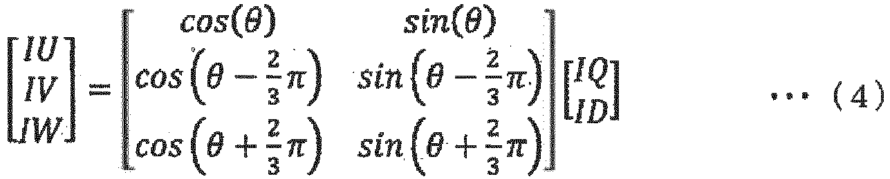
- AC voltage commands VUParef, VVParef, VWParef, which are given to the arm converters 17UP, 17VP, 17WP, and AC voltage commands VUNaref, WNaref, VWNaref, which are given to the arm converters 17UN, 17VN, 17WN are generated from the VUref, VVref, Vwref. A DC voltage command VDCref/2 is added to the AC voltage command to calculate arm voltage commands VUPref, VUNref, VVPref, WNref, VWPref, VWNref.
- The dead
time calculation unit 38 implements a function of preventing both theupper switching element 24H and thelower switching element 24L from being turned ON simultaneously by adding the dead time to the gate pulse derived from thePWM calculation unit 31. - In the period from the time t2d to t3d as shown in
FIG. 9 , currents IRDA, IRDB, IRDC each flowing to thedischarge resistance 9 is reduced on the ground that the Q-axis currentcommand calculation unit 37 as shown inFIG. 10 calculates the Q-axis current command IQref to be changed in accordance with the DC voltage VDC. The following is the reason for changing the Q-axis current command IQref in accordance with the DC voltage VDC in the period from the time t2d to t3d. - Assuming that the discharging operation is continued in the period from the time t2d to t3d based on the IQref as the constant current command, the DC voltage VDC is lowered as the drop of the capacitor voltage into the over-modulation operation region. As a result, the IQ cannot follow the IQref. In order to avoid this, the Q-axis current
command calculation unit 37 calculates the Q-axis current command IQref in accordance with the DC voltage VDC. Specifically, the IQref is set to satisfy the formula (5). The term R denotes a resistance value of thedischarge resistance 9, and the term X denotes a leakage reactance, of the tappedinitial charge transformer 14.
[formula 5]
- After discharging the capacitor up to the target voltage, at the time t3d, all breakers are set to "open", and the gate pulse output flags FLG_GDB of the
DSMMC converters DSMCC - The initial charging operation as described above allows simultaneous charging of the capacitor of the power conversion apparatus constituted by two units of the DSMMC converters while preventing the rush overcurrent during the initial charging operation. This makes it possible to reduce the time for starting and stopping the power conversion apparatus. During the discharging operation, the
initial charge transformer 14 is tapped to implement the function for adjusting the power source voltage value by switching the tap of the transformer. Compared with the means disclosed inPatent Literature 2, the regenerative operation range during the discharging operation is expanded to reduce the energy consumed by the discharge resistance by approximately 80%. -
FIG. 11 shows an example of a main circuit structure of a power conversion apparatus according to a fourth embodiment of the present invention.FIG. 11 is different fromFIG. 1 according to the first embodiment in that the initial charging device 4 does not include thedischarge resistance 9 and thedischarge breaker 11 therein. Theinitial charge resistance 10 serves to implement the function of the eliminated discharge resistance, and theinitial charge breaker 12 serves to implement the function of the discharge breaker. - The structure as shown in
FIG. 11 allows further downsizing of the initial charging device. - 1A, 1B: DSMMC converter, 2A, 2B: three-phase power source, 3: voltage phase detection unit, 4: initial charging device, 5: 6A, 6B: main circuit breaker, 7: initial charging device breaker, 8: three-phase short-circuit breaker, 9: discharge resistance, 10: initial charge resistance, 11: discharge breaker, 12: initial charge breaker, 13: resistance bypass breaker, 14: tapped initial charge transformer, 15, 16: transformer tap switch breaker, 17UP, 17UN, 17VP, 17VN, 17WP, 17WN: arm converter, 18, 21P, 21N: current detector, 19: circulating current suppression reactor, 20P, 20N: high resistance, 23: unit converter, 24H, 24L: switching element, 25: capacitor, 26: voltage detector, 28H, 28L: gate drive unit (GDU), 29: signal converter, 30: modulation factor determination unit, 31: PWM calculation unit, 32: gate pulse output determination circuit, 33: AC current calculation unit, 34: three-phase/two-phase conversion unit, 35: AC current control unit, 36: three-phase/two-phase inverse conversion unit, 37: Q-axis current command calculation unit, 38: dead time calculation unit
Claims (6)
- A power conversion apparatus comprising a unit converter which is formed through parallel connection of a capacitor and a switching circuit constituted by two sets of series-connected switching elements having reflux diodes connected in parallel, a power converter which forms an arm having circulating current suppression reactors connected in series, forms a leg by two sets of the arms connected in series, and connects a connection point of the two sets of the arms, serving as an AC terminal to a phase of a first AC power source to cause both ends of the leg to serve as DC terminals, and a charging and discharging device having one end connected to a second AC power source, and the other end connected to the phase of the first AC power source,
wherein the charging and discharging device includes a tapped transformer which makes a position switchable between a full-tap position and a half-tap position, and is connected to the power converter instead of the first AC power source when starting and stopping the power converter. - The power conversion apparatus according to claim 1,
wherein a high-voltage tap position of the tapped transformer is connected when starting the power converter, and a low-voltage tap position of the tapped transformer is connected when stopping the power converter. - A control apparatus of a power conversion apparatus provided with a unit converter which is formed through parallel connection of a capacitor and a switching circuit constituted by two sets of series-connected switching elements having reflux diodes connected in parallel, a power converter which forms an arm having circulating current suppression reactors connected in series, forms a leg by two sets of the arms connected in series, and connects a connection point of the two sets of the arms to a phase of a first AC power source to cause both ends of the leg to serve as DC terminals, and a charging and discharging device having one end connected to a second AC power source, and the other end connected to the phase of the first AC power source, wherein:the charging and discharging device includes a tapped transformer which makes a position switchable between a high-voltage tap position and a low-voltage tap position, and is connected to the power converter instead of the first AC power source when starting and stopping the power converter; andthe control apparatus makes a transition from a resistance charging mode to a bypass charging mode, and further to a switching charging mode for turn-on of the unit converter to connect the first AC power source instead of the second AC power source to the power converter, the resistance charging mode having the second AC power source connected to an AC terminal of the power converter via a resistance and the high-voltage tap position of the tapped transformer when starting the power converter, and the bypass charging mode having connection to the AC terminal of the power converter from the second AC power source via the tapped transformer.
- The control apparatus of the power conversion apparatus according to claim 3,
wherein the control apparatus controls to increase a PWM modulation factor of a gate pulse given to the switching circuit with the lapse of time in the switching charging mode for turn-on of the unit converter. - The control apparatus of the power conversion apparatus according to claim 3,
wherein the control apparatus applies an OFF signal to a gate pulse given to one of two sets of series-connected switching elements constituting the switching circuit in the switching charging mode for turn-on of the unit converter to prevent the capacitor connected to the switching circuit in parallel from being brought into a discharge state. - A control apparatus of a power conversion apparatus including a unit converter which is formed through parallel connection of a capacitor and a switching circuit constituted by two sets of series-connected switching elements having reflux diodes connected in parallel, a power converter which forms an arm having circulating current suppression reactors connected in series, forms a leg by two sets of the arms connected in series, and connects a connection point of the two sets of the arms to a phase of a first AC power source to cause both ends of the leg to serve as DC terminals, and a charging and discharging device having one end connected to a second AC power source, and the other end connected to the phase of the first AC power source, wherein:the charging and discharging device includes a tapped transformer which makes a position switchable between a high-voltage tap position and a low-voltage tap position, and is connected to the power converter instead of the first AC power source when starting and stopping the power converter; andthe control apparatus makes a transition from a regenerative discharging mode to a resistance discharging mode, in the regenerative discharging mode, the second AC power source instead of the first AC power source is connected via the low-voltage tap position of the tapped transformer when stopping the power converter, and a gate pulse with a PWM modulation factor determined by a current control unit is given to the switching element to operate the power converter, and in the resistance discharging mode, the second AC power source is connected via the resistance from the low-voltage tap position of the tapped transformer to operate the power converter.
Applications Claiming Priority (2)
| Application Number | Priority Date | Filing Date | Title |
|---|---|---|---|
| JP2021128800A JP7710334B2 (en) | 2021-08-05 | 2021-08-05 | Power conversion device and its control device |
| PCT/JP2022/029999 WO2023013735A1 (en) | 2021-08-05 | 2022-08-04 | Power conversion apparatus and control apparatus for same |
Publications (2)
| Publication Number | Publication Date |
|---|---|
| EP4383550A1 true EP4383550A1 (en) | 2024-06-12 |
| EP4383550A4 EP4383550A4 (en) | 2025-08-13 |
Family
ID=85155848
Family Applications (1)
| Application Number | Title | Priority Date | Filing Date |
|---|---|---|---|
| EP22853153.9A Pending EP4383550A4 (en) | 2021-08-05 | 2022-08-04 | POWER CONVERSION DEVICE AND CONTROL DEVICE THEREFOR |
Country Status (3)
| Country | Link |
|---|---|
| EP (1) | EP4383550A4 (en) |
| JP (1) | JP7710334B2 (en) |
| WO (1) | WO2023013735A1 (en) |
Family Cites Families (7)
| Publication number | Priority date | Publication date | Assignee | Title |
|---|---|---|---|---|
| JP5675152B2 (en) * | 2010-04-09 | 2015-02-25 | 株式会社日立製作所 | Power converter |
| JP5495319B2 (en) * | 2010-05-11 | 2014-05-21 | ニチコン株式会社 | Power storage device |
| JP5775033B2 (en) | 2012-07-11 | 2015-09-09 | 株式会社日立製作所 | Control device and control method for voltage type power converter |
| JP6099951B2 (en) * | 2012-11-29 | 2017-03-22 | 株式会社東芝 | Power converter |
| EP2988404A1 (en) * | 2014-08-22 | 2016-02-24 | ABB Technology AG | Modular multilevel converter precharge |
| EP3890134B1 (en) * | 2018-11-28 | 2024-03-06 | Mitsubishi Electric Corporation | Power control system |
| WO2020250358A1 (en) * | 2019-06-12 | 2020-12-17 | 三菱電機株式会社 | Power conversion device |
-
2021
- 2021-08-05 JP JP2021128800A patent/JP7710334B2/en active Active
-
2022
- 2022-08-04 WO PCT/JP2022/029999 patent/WO2023013735A1/en not_active Ceased
- 2022-08-04 EP EP22853153.9A patent/EP4383550A4/en active Pending
Also Published As
| Publication number | Publication date |
|---|---|
| EP4383550A4 (en) | 2025-08-13 |
| JP2023023350A (en) | 2023-02-16 |
| JP7710334B2 (en) | 2025-07-18 |
| WO2023013735A1 (en) | 2023-02-09 |
Similar Documents
| Publication | Publication Date | Title |
|---|---|---|
| US10483871B2 (en) | Power conversion apparatus and power system | |
| EP3231053B1 (en) | Standby and charging of modular multilevel converters | |
| EP2506422B1 (en) | Circuits for dc energy stores | |
| US11223310B2 (en) | Variable speed generator/motor device | |
| CN111786396B (en) | Commutation failure suppression method for high voltage DC transmission system based on energy storage chain STATCOM | |
| US11309787B2 (en) | Power conversion device | |
| US8614903B2 (en) | Power conditioner for photovoltaic power generation | |
| US10110110B2 (en) | Power conversion device | |
| US11239664B2 (en) | Power conversion system | |
| JP2018537945A (en) | Active discharge of modular multilevel converters. | |
| US20260018991A1 (en) | Power conversion device and offshore wind power generation system | |
| EP4117155A1 (en) | Power converter systems | |
| CN114123840A (en) | High-output-power wide-voltage direct-current power supply | |
| CN117879020A (en) | A unloading submodule, a hybrid DC unloading device and a control method | |
| EP3961847A1 (en) | Power supply device | |
| EP3823158A1 (en) | Variable-speed generator-motor device | |
| EP3796536B1 (en) | Power conversion device | |
| EP4383550A1 (en) | Power conversion apparatus and control apparatus for same | |
| EP3893374B1 (en) | Power converter systems with integrated energy storage | |
| US12068679B2 (en) | Power conversion device preventing overcurrent at the time of starting | |
| CN112311217A (en) | Hybrid MMC controlled charging control method with buffer circuit | |
| EP4654456A1 (en) | Modular multi-level electric power converter | |
| US20240305188A1 (en) | Power Conversion Device | |
| EP4525017A2 (en) | Modular multilevel converters | |
| EP4402786B1 (en) | Charging of a modular multilevel converter |
Legal Events
| Date | Code | Title | Description |
|---|---|---|---|
| STAA | Information on the status of an ep patent application or granted ep patent |
Free format text: STATUS: THE INTERNATIONAL PUBLICATION HAS BEEN MADE |
|
| PUAI | Public reference made under article 153(3) epc to a published international application that has entered the european phase |
Free format text: ORIGINAL CODE: 0009012 |
|
| STAA | Information on the status of an ep patent application or granted ep patent |
Free format text: STATUS: REQUEST FOR EXAMINATION WAS MADE |
|
| 17P | Request for examination filed |
Effective date: 20240305 |
|
| AK | Designated contracting states |
Kind code of ref document: A1 Designated state(s): AL AT BE BG CH CY CZ DE DK EE ES FI FR GB GR HR HU IE IS IT LI LT LU LV MC MK MT NL NO PL PT RO RS SE SI SK SM TR |
|
| DAV | Request for validation of the european patent (deleted) | ||
| DAX | Request for extension of the european patent (deleted) | ||
| REG | Reference to a national code |
Ref country code: DE Ref legal event code: R079 Free format text: PREVIOUS MAIN CLASS: H02M0007497000 Ipc: H02M0001360000 |
|
| A4 | Supplementary search report drawn up and despatched |
Effective date: 20250711 |
|
| RIC1 | Information provided on ipc code assigned before grant |
Ipc: H02M 1/36 20070101AFI20250707BHEP Ipc: H02M 1/32 20070101ALI20250707BHEP Ipc: H02M 7/483 20070101ALI20250707BHEP |