EP4383108A1 - Control apparatus and robot system - Google Patents
Control apparatus and robot system Download PDFInfo
- Publication number
- EP4383108A1 EP4383108A1 EP23212827.2A EP23212827A EP4383108A1 EP 4383108 A1 EP4383108 A1 EP 4383108A1 EP 23212827 A EP23212827 A EP 23212827A EP 4383108 A1 EP4383108 A1 EP 4383108A1
- Authority
- EP
- European Patent Office
- Prior art keywords
- work area
- program
- board
- area
- compressed file
- Prior art date
- Legal status (The legal status is an assumption and is not a legal conclusion. Google has not performed a legal analysis and makes no representation as to the accuracy of the status listed.)
- Granted
Links
Images




Classifications
-
- G—PHYSICS
- G06—COMPUTING OR CALCULATING; COUNTING
- G06F—ELECTRIC DIGITAL DATA PROCESSING
- G06F21/00—Security arrangements for protecting computers, components thereof, programs or data against unauthorised activity
- G06F21/50—Monitoring users, programs or devices to maintain the integrity of platforms, e.g. of processors, firmware or operating systems
- G06F21/57—Certifying or maintaining trusted computer platforms, e.g. secure boots or power-downs, version controls, system software checks, secure updates or assessing vulnerabilities
- G06F21/575—Secure boot
-
- B—PERFORMING OPERATIONS; TRANSPORTING
- B25—HAND TOOLS; PORTABLE POWER-DRIVEN TOOLS; MANIPULATORS
- B25J—MANIPULATORS; CHAMBERS PROVIDED WITH MANIPULATION DEVICES
- B25J9/00—Program-controlled manipulators
- B25J9/16—Program controls
- B25J9/1602—Program controls characterised by the control system, structure, architecture
- B25J9/161—Hardware, e.g. neural networks, fuzzy logic, interfaces, processor
-
- B—PERFORMING OPERATIONS; TRANSPORTING
- B25—HAND TOOLS; PORTABLE POWER-DRIVEN TOOLS; MANIPULATORS
- B25J—MANIPULATORS; CHAMBERS PROVIDED WITH MANIPULATION DEVICES
- B25J9/00—Program-controlled manipulators
- B25J9/16—Program controls
- B25J9/1602—Program controls characterised by the control system, structure, architecture
-
- B—PERFORMING OPERATIONS; TRANSPORTING
- B25—HAND TOOLS; PORTABLE POWER-DRIVEN TOOLS; MANIPULATORS
- B25J—MANIPULATORS; CHAMBERS PROVIDED WITH MANIPULATION DEVICES
- B25J13/00—Controls for manipulators
-
- B—PERFORMING OPERATIONS; TRANSPORTING
- B25—HAND TOOLS; PORTABLE POWER-DRIVEN TOOLS; MANIPULATORS
- B25J—MANIPULATORS; CHAMBERS PROVIDED WITH MANIPULATION DEVICES
- B25J9/00—Program-controlled manipulators
- B25J9/0096—Program-controlled manipulators co-operating with a working support, e.g. work-table
-
- G—PHYSICS
- G06—COMPUTING OR CALCULATING; COUNTING
- G06F—ELECTRIC DIGITAL DATA PROCESSING
- G06F21/00—Security arrangements for protecting computers, components thereof, programs or data against unauthorised activity
- G06F21/50—Monitoring users, programs or devices to maintain the integrity of platforms, e.g. of processors, firmware or operating systems
- G06F21/57—Certifying or maintaining trusted computer platforms, e.g. secure boots or power-downs, version controls, system software checks, secure updates or assessing vulnerabilities
- G06F21/572—Secure firmware programming, e.g. of basic input output system [BIOS]
-
- G—PHYSICS
- G06—COMPUTING OR CALCULATING; COUNTING
- G06F—ELECTRIC DIGITAL DATA PROCESSING
- G06F21/00—Security arrangements for protecting computers, components thereof, programs or data against unauthorised activity
- G06F21/60—Protecting data
- G06F21/64—Protecting data integrity, e.g. using checksums, certificates or signatures
-
- B—PERFORMING OPERATIONS; TRANSPORTING
- B25—HAND TOOLS; PORTABLE POWER-DRIVEN TOOLS; MANIPULATORS
- B25J—MANIPULATORS; CHAMBERS PROVIDED WITH MANIPULATION DEVICES
- B25J9/00—Program-controlled manipulators
- B25J9/16—Program controls
- B25J9/1656—Program controls characterised by programming, planning systems for manipulators
- B25J9/1661—Program controls characterised by programming, planning systems for manipulators characterised by task planning, object-oriented languages
Definitions
- the present disclosure relates to a control apparatus and a robot system.
- JP-A-2007-086920 discloses an electronic apparatus configured to activate the electronic apparatus by reading in and executing a program stored in external memory means. According to the electronic apparatus, even when a boot program stored in a read-only memory (ROM) or the ROM itself is defective, the electronic apparatus can be activated. Thereby, time and effort for repairing including replacement of the ROM may be saved.
- ROM read-only memory
- An electronic apparatus may include a main board at least for activation and a sub-board for functionality expansion.
- a program necessary for activation is once read out from external memory means into a memory of the main board, and then, a processor of the main board executes processing of loading programs for the respective boards.
- the loading processing is performed after the programs for the respective boards are read in a work area of the memory of the main board. Accordingly, the work area of the main board is temporarily reduced and the speed of the loading processing and the speed of the activation processing of the main board become lower. As a result, a problem that time is taken for activation of the electronic apparatus arises.
- a control apparatus includes a first board having a first memory unit containing a first work area and a first coupling area and a first processing unit executing a first program stored in the first work area, a second board having a second memory unit containing a second work area and a second processing unit executing a second program stored in the second work area, a communication interface linking the first coupling area and the second work area, and a memory medium storing a compressed file containing the first program and the second program, wherein the compressed file is read out from the memory medium into the first work area, the first program contained in the compressed file is loaded in the first work area, the second program contained in the compressed file is loaded in the first coupling area, and the second program is transferred from the first coupling area to the second work area via the communication interface.
- a robot system includes a robot including a robot arm, and the control apparatus according to the application example of the present disclosure controlling a motion of the robot.
- FIG. 1 is a conceptual diagram showing a robot system 1 according to the embodiment.
- the robot system 1 shown in FIG. 1 includes a robot 100, a control apparatus 200 (a control apparatus according to the embodiment), a teach pendant 300, a personal computer 350, and a display unit 360.
- the robot 100 shown in FIG. 1 includes a base 120 and a robot arm 130.
- the robot arm 130 includes six arms coupled sequentially from the base 120 side and six joints J1 to J6 coupling between the base 120 and the arm and between the arms.
- the three joints J2, J3, J5 are bending joints and the other three joints J1, J4, J6 are twisting joints.
- Each of the joints J1 to J6 includes a motor as a drive source and an encoder for detecting a rotation amount of the motor, i.e., position information of the motor (not shown).
- the motor and the encoder are combined as a servo motor.
- a control point showing a position of the robot arm 130 as an object to be controlled is set at a distal end of the robot arm 130.
- a six-axis vertical articulated robot is exemplified as the robot 100, however, the number of axes is not particularly limited, but may be more or less than six. Or, the robot 100 may be a horizontal articulated robot, a dual-arm robot, or a robot having another form.
- An arm end 132 is provided at the distal end of the robot arm 130, i.e., an end of the robot arm 130 opposite to the base 120.
- An end effector 160 is attached to the arm end 132.
- the end effector 160 is detachably attached.
- the end effector 160 includes e.g., a hand gripping a workpiece and a suction tool suctioning a work piece.
- FIG. 2 is a block diagram showing a hardware configuration of the control apparatus 200 shown in FIG. 1 .
- the control apparatus 200 shown in FIG. 2 includes a main board 220 (first board), a first sub-board 240 (second board), and a second sub-board 260 (third board). These respective boards can communicate with one another via a communication interface 280.
- the main board 220 shown in FIG. 2 includes a printed wiring board 221, a processor 222 (first processing unit), a system bus 226, a RAM 228 (first memory unit), a ROM 230, an input/output port 232, a memory card interface 234, and a memory card 290 (memory medium).
- the RAM is abbreviated for Random Access Memory and the ROM is abbreviated for Read-Only Memory.
- the printed wiring board 221 includes an insulated substrate and wires and electrically couples attached electronic components.
- the processor 222 realizes various functions by executing a first program loaded in the RAM 228.
- the processor 222 includes e.g., a microprocessor, a core, and a processor circuit having a cache memory etc. (not shown).
- the microprocessor and the core include e.g., CPUs (Central Processing Units) and DSPs (Digital Signal Processors).
- the processor circuit includes e.g., a SoC (System on a Chip) and a SiP (System in a Package). Or, a part or all of the processor 222 may be formed by a device such as an ASIC (Application Specific Integrated Circuit) or an FPGA (Field Programmable Gate Array).
- ASIC Application Specific Integrated Circuit
- FPGA Field Programmable Gate Array
- the system bus 226 is a transmission route coupling between the processor 222 and the RAM 228 and ROM 230 for enabling mutual communication.
- the RAM 228 temporarily stores the first program to be executed by the processor 222, read-out data, etc.
- the RAM 228 includes e.g., a DRAM (Dynamic Random Access Memory).
- the ROM 230 stores a boot program to be executed by the processor 222 etc.
- the ROM 230 includes e.g., an EEPROM (registered trademark) (Electrically Erasable Programmable Read-Only Memory) and a Flash ROM (Flash Read-Only Memory). Note that the ROM 230 may be an external memory.
- the input/output port 232 is an interface for communication between the respective units of the main board 220 and another apparatus.
- the input/output port 232 includes e.g., a digital input/output port such as a USB (Universal Serial Bus), an Ethernet (registered trademark) port, and a picture output port.
- a digital input/output port such as a USB (Universal Serial Bus), an Ethernet (registered trademark) port, and a picture output port.
- the memory card interface 234 is an interface for the memory card 290 (memory medium) to be detachable.
- the memory card interface 234 reads out a file stored in the attached memory card 290 and writes a file in the attached memory card 290.
- a compressed file 400 which will be described later, is stored in the memory card 290.
- the memory card 290 includes e.g., various memory media such as an SD card and a USB memory.
- the memory media are data-writable and non-volatile.
- the memory medium may be easily replaced by a memory card 290 storing a new compressed file 400, and the new compressed file 400 may be introduced into the main board 220 easily in a short time.
- the memory card 290 is detachable and external data may be easily read in the main board 220.
- the memory card 290 may be undetachable and, in this case, may be fixed to the control apparatus 200 as a mere memory medium. Further, data may be downloaded in the memory medium via a network or the like.
- the first sub-board 240 shown in FIG. 2 includes a printed wiring board 241, a processor 242 (second processing unit), a system bus 246, and a RAM 248 (second memory unit).
- the printed wiring board 241 includes an insulated substrate and wires and electrically couples attached electronic components.
- the processor 242 realizes various functions by executing a second program loaded in the RAM 248.
- the processor 242 includes e.g., a microprocessor, a core, and a processor circuit having a cache memory etc. (not shown). Or, a part or all of the processor 242 may be formed by a device such as an ASIC or an FPGA.
- the system bus 246 enables communication between the processor 242 and the RAM 248.
- the RAM 248 temporarily stores the second program to be executed by the processor 242, read-out data, etc.
- the second sub-board 260 shown in FIG. 2 includes a printed wiring board 261, a processor 262 (third processing unit), a system bus 266, and a RAM 268 (third memory unit).
- the printed wiring board 261 includes an insulated substrate and wires and electrically couples attached electronic components.
- the processor 262 realizes various functions by executing a third program loaded in the RAM 268.
- the processor 262 includes e.g., a microprocessor, a core, and a processor circuit having a cache memory etc. (not shown). Or, a part or all of the processor 262 may be formed by a device such as an ASIC or an FPGA.
- the system bus 266 enables communication between the processor 262 and the RAM 268.
- the RAM 268 temporarily stores the third program to be executed by the processor 262, read-out data, etc.
- the communication interface 280 is a transmission route for transmission of programs, data, etc., e.g., a serial communication interface such as a PCI or PCI-Express (registered trademark) or the like.
- a serial communication interface such as a PCI or PCI-Express (registered trademark) or the like.
- PCI-Express registered trademark
- PCle PCI-Express
- the hardware configuration example of the control apparatus 200 is explained, however, the hardware configuration is not limited to that.
- the second sub-board 260 may be omitted or another sub-board may be added.
- FIG. 3 is a functional block diagram showing functions of the control apparatus 200 shown in FIG. 2 .
- the main board 220 shown in FIG. 3 has an interface control unit 312, a language analysis unit 314, an input/output control unit 316, an interrupt control unit 318, and an activation processing unit 320 as functional units.
- the functions of these respective functional units are realized by e.g., the processor 222 executing the first program stored in the RAM 228 of the main board 220 and the boot program stored in the ROM 230 depending on the hardware configuration of the main board 220.
- the interface control unit 312 controls communication among the main board 220, the first sub-board 240, and the second sub-board 260.
- the language analysis unit 314 reads and analyzes a robot language describing a motion of the robot 100.
- the unit receives a motion program of the robot 100 from the personal computer 350 via the input/output control unit 316, which will be described later, analyzes the motion program, and acquires target position information of the robot arm 130.
- the target position information is information on a target position as a target location to which the control point of the robot arm 130 is moved, e.g., data representing coordinates of the target position.
- the input/output control unit 316 controls coupling to the teach pendant 300, the personal computer 350, and another peripheral device coupled to the main board 220.
- the interrupt control unit 318 controls processing of branching from a program being executed to another program (interrupt processing).
- the activation processing unit 320 has a function of activating the main board 220.
- the activation processing unit 320 has a hardware initialization section 322, a program readout section 324, a program certification section 326, a program loading section 328, and a program execution section 330.
- the hardware initialization section 322 initializes at least the main board 220 and the communication interface 280.
- the program readout section 324 reads out a file stored in the memory card 290. Then, the program readout section 324 copies the read-out file in the RAM 228.
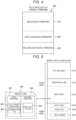
- FIG. 4 shows a file structure of overall firmware 440 stored in the memory card 290 in FIG. 2 .
- the overall firmware 440 has a main board firmware 410 (first program), a first sub-board firmware 420 (second program), and a second sub-board firmware 430 (third program).
- Each firmware is a program containing e.g., an OS (operating system), an application, data, etc.
- the overall firmware 440 is generally in a binary format, but may be in a text format.
- FIG. 5 shows a memory map of the memory card 290 shown in FIG. 2 and a memory map of the main board 220 shown in FIG. 2 .
- the memory map shown in FIG. 5 is an example and the memory map is not limited to that.
- the RAM 228 of the main board 220 contains memory spaces including a PCIe link area 512 (first coupling area), a peripheral area 514, a work area 516 (first work area), and a boot area 518. Of the areas, the boot area 518 stores a public key 542 and a bootloader 544.
- the memory space of the memory card 290 is divided in a first partition 291 and a second partition 292.
- the first partition 291 stores the compressed file 400 and an electronic signature 405.
- the second partition 292 stores a root file system 403.
- the compressed file 400, the electronic signature 405, and the root file system 403 shown in FIG. 5 are copied in the work area 516 in the activation processing of the control apparatus 200, which will be described later.
- the program certification section 326 certifies the compressed file 400 read out in the RAM 228.
- the certification refers to verification of integrity and authenticity of the compressed file 400.
- a status that the integrity and the authenticity are confirmed is referred to as "certified”.
- the program loading section 328 loads the main board firmware 410 of the certified compressed file 400 in the work area 516 of the RAM 228 of the main board 220. Further, the program loading section 328 loads the first sub-board firmware 420 and the second sub-board firmware 430 of the certified compressed file 400 in the PCIe link area 512 of the RAM 228.
- the program execution section 330 executes the certified main board firmware 410. Thereby, the main board 220 is activated.
- these functional units of the main board 220 are examples and may be partially omitted or partially provided on another board, and another functional unit may be added.
- the first sub-board 240 shown in FIG. 3 has a trajectory generation unit 332 and an activation processing unit 336 as functional units.
- the functions of these respective functional units are realized by e.g., the processor 242 executing the second program stored in the RAM 248 of the first sub-board 240 depending on the hardware configuration of the first sub-board 240.
- the trajectory generation unit 332 generates a trajectory when the robot arm 130 is driven based on the target position information received from the main board 220.
- the activation processing unit 336 executes the certified first sub-board firmware 420. Thereby, the first sub-board 240 is activated.
- these functional units of the first sub-board 240 are examples and may be partially omitted or partially provided in another board, and another functional unit may be added.
- the second sub-board 260 shown in FIG. 3 has a servo processing unit 342 and an activation processing unit 346 as functional units.
- the functions of these respective functional units are realized by e.g., the processor 262 executing the second program stored in the RAM 248 of the second sub-board 260 depending on the hardware configuration of the second sub-board 260.
- the servo processing unit 342 controls an operation of the servo motor of the robot 100.
- the activation processing unit 346 executes the certified second sub-board firmware 430. Thereby, the second sub-board 260 is activated.
- these functional units of the second sub-board 260 are examples and may be partially omitted or partially provided in another board, and another functional unit may be added.
- FIG. 6 is a flowchart for explanation of the activation method for the control apparatus 200.
- FIGS. 7 to 10 are conceptual diagrams for explanation of the activation method shown in FIG. 6 .
- the activation method for the control apparatus 200 shown in FIG. 6 has step S102 to step S114.
- step S102 the program readout section 324 of the activation processing unit 320 performs processing of reading out the public key 542 and the bootloader 544 stored in the boot area 518 shown in FIG. 5 .
- the program certification section 326 performs processing of certifying the public key 542 and the bootloader 544.
- the certification processing is processing of verifying integrity and authenticity of the public key 542 and the bootloader 544.
- the hardware initialization section 322 initializes the main board 220 and the communication interface 280.
- the program execution section 330 executes the bootloader 544. Thereby, preparation for execution of the firmwares is made.
- the program readout section 324 reads out the compressed file 400, the electronic signature 405, and the root file system 403 stored in the memory card 290 in the work area 516.
- the electronic signature 405 is a digital signature associated with the compressed file 400.
- the compressed file 400 is a file formed by data compression of the overall firmware 440.
- the root file system 403 is a root file system of each firm ware.
- the overall firmware 440 is data-compressed and the compressed file 400 is obtained.
- the compressed file 400 is stored in the memory card 290 without change.
- the overall firmware 440 is compressed and stored, and thereby, data capacity of the memory card 290 may be reduced and time taken for reading out and loading of the stored compressed file may be reduced.
- a hash function is executed on the compressed file 400. Thereby, a hash value 401 is obtained.
- the hash function is a function of returning output data (hash value) having a fixed length from data having an arbitrary length and has a property of returning the same hash value from the same data.
- the hash function includes e.g., SHA-258, SHA-384, and SHA-512.
- the obtained hash value 401 is encrypted using a secret key 402.
- the encryption of the hash value 401 may be performed by e.g., a certificate authority as a certification institution using the secret key 402.
- the electronic signature 405 is obtained.
- the electronic signature 405 is stored in the memory card 290.
- the program certification section 326 certifies the compressed file 400 based on the electronic signature 405 read out in the work area 516.
- the read-out electronic signature 405 is decrypted using the public key 542.
- the public key 542 forms a pair with the above-described secret key 402 and is issued from the certificate authority in advance.
- a hash value 407 (first hash value) is generated.
- the hash function is executed on the compressed file 400.
- a hash value 408 (second hash value) is generated.
- the hash value 407 and the hash value 408 are compared.
- the certification of the compressed file 400 may be achieved only by comparison between the values having fixed lengths as hash values. Accordingly, the certification may be achieved in a shorter time and that contributes to shortening of the activation time of the control apparatus 200. Further, it is preferable that the public key 542 is stored in the control apparatus 200. Thereby, the certification processing may be performed in a local environment and that contributes to further shortening of the activation time.
- step S111 whether the compressed file 400 is certified is determined.
- the process goes to step S112.
- the control apparatus 200 may be activated only when the file is certified and secure boot is realized.
- the program loading section 328 loads the respective firmwares from the compressed file 400.
- FIGS. 9 and 10 are respectively for explanation of the processing of loading the respective firmwares from the compressed file 400.
- the main board 220 contains the PCIe link area 512 (first coupling area), the peripheral area 514, and the work area 516 (first work area) as the memory spaces.
- the PCIe link area 512 contains a first sub-board link area 512a and a second sub-board link area 512b.
- the peripheral area 514 is a memory space provided to a peripheral device coupled to the main board 220.
- the work area 516 is a memory space accessed by the processor 222. Note that these memory spaces are set in e.g., the RAM 228, however, may be set in another memory device. Further, the setting of the memory spaces is performed by e.g., a controller (not shown) contained in the chipset of the communication interface 280.
- the first sub-board 240 contains a PCIe link area 522 (second coupling area) and a work area 526 (second work area) as memory spaces.
- the PCIe link area 522 contains a second sub-board link area 522b.
- the work area 526 is a memory space accessed by the processor 242. Note that these memory spaces are set in e.g., the RAM 248, however, may be set in another memory device.
- the second sub-board 260 contains a work area 536 (third work area) as a memory space.
- the work area 536 is a memory space accessed by the processor 262.
- the first sub-board link area 512a is linked to the work area 526 via the communication interface 280.
- the second sub-board link area 512b is mutually linked to the second sub-board link area 522b and the work area 536 via the communication interface 280.
- the program loading section 328 extracts the main board firmware 410 (first program) from the compressed file 400 and loads the firmware in the work area 516 of the main board 220. Further, as shown in FIG. 9 , the program loading section 328 extracts the first sub-board firmware 420 (second program) from the compressed file 400 and loads the firmware in the first sub-board link area 512a contained in the PCIe link area 512 (first coupling area) of the main board 220. Furthermore, as shown in FIG.
- the program loading section 328 extracts the second sub-board firmware 430 (third program) from the compressed file 400 and loads the firmware in the second sub-board link area 512b contained in the PCIe link area 512 of the main board 220.
- the loading processing is performed by e.g., the processor 222 or the controller (not shown) contained in the chipset of the communication interface 280.
- the section may load the respective firmwares remaining in the compressed conditions or in decompressed conditions.
- the firmwares may be decompressed in the respective boards.
- the first sub-board firmware 420 is transferred from the first sub-board link area 512a contained in the PCIe link area 512 (first coupling area) to the work area 526 (second work area) of the first sub-board 240 via the communication interface 280.
- the second sub-board firmware 430 is transferred from the second sub-board link area 512b contained in the PCIe link area 512 (first coupling area) through the PCIe link area 522 (second coupling area) of the first sub-board 240 to the work area 536 (third work area) of the second sub-board 260 via the communication interface 280.
- the loading processing is performed by e.g., the controller (not shown) contained in the chipset of the communication interface 280. Thereby, the transfer processing may be performed with the minimized load on the processor 222.
- the respective firmwares may be loaded in the respective work areas. Then, the respective firmwares are executed in the respective work areas, and thereby, the respective boards may be activated and the activation of the control apparatus 200 is completed.
- the first sub-board firmware 420 is transferred from the PCIe link area 512 to the work area 526 of the first sub-board 240 and the second sub-board firmware 430 is transferred from the PCIe link area 512 through the PCIe link area 522 to the work area 536 of the second sub-board 260.
- the work area 516 of the main board 220 may be avoided from being occupied by the loading and the transfer of the respective firmwares.
- the temporal reduction of the work area 516 may be suppressed and the reduction of the processing speed of the processor 222 of the main board 220 may be suppressed.
- the respective firmwares can be transferred. Accordingly, the reduction of the operation speed of the processor 222 with the transfer of the respective firmwares may be suppressed. Therefore, the activation time of the control apparatus 200 may be shortened using the above-described activation method.
- the system of reading out the compressed file 400 is employed, and therefore, compared to a case where an uncompressed firmware is read out, data capacity of the memory card 290 may be reduced. Thereby, the time taken to read out the firmware may be reduced.
- control apparatus 200 includes the main board 220 (first board), the first sub-board 240 (second board), the communication interface 280, and the memory card 290 (memory medium) as shown in FIGS. 1 and 2 .
- the main board 220 has the RAM 228 (first memory area) containing the work area 516 (first work area) and the PCIe link area 512 (first coupling area) and the processor 222 (first processing unit) executing the main board firmware 410 (first program) stored in the work area 516.
- the first sub-board 240 has the RAM 248 (second memory unit) containing the work area 526 (second work area) and the processor 242 (second processing unit) executing the first sub-board firmware 420 (second program) stored in the work area 526.
- the communication interface 280 links the PCIe link area 512 and the work area 526.
- the memory card 290 (memory medium) stores the compressed file 400 containing the main board firmware 410 and the first sub-board firmware 420.
- control apparatus 200 reads out the compressed file 400 from the memory card 290 into the work area 516, loads the main board firmware 410 contained in the compressed file 400 in the work area 516, loads the first sub-board firmware 420 contained in the compressed file 400 in the PCIe link area 512, and transfers the first sub-board firmware 420 from the PCIe link area 512 to the work area 526 via the communication interface 280.
- the work area 516 of the main board 220 may be avoided from being occupied by the loading and the transfer of the respective firmwares.
- the temporal reduction of the work area 516 may be suppressed and the reduction of the processing speed of the processor 222 of the main board 220 may be suppressed.
- the respective firmwares can be transferred. Accordingly, the reduction of the operation speed of the processor 222 with the transfer of the respective firmwares may be suppressed. Therefore, according to the above-described configuration, the activation time of the control apparatus 200 may be shortened.
- the memory card 290 (memory medium) stores the electronic signature 405 associated with the compressed file 400.
- control apparatus 200 performs the certification processing of certifying the compressed file 400 based on the electronic signature 405, when the compressed file is certified in the certification processing, loads the main board firmware 410 (first program) and the first sub-board firmware 420 (second program) and, when the compressed file is not certified, does not load the main board firmware 410 and the first sub-board firmware 420.
- the secure boot of the control apparatus 200 may be realized. That is, the activation of the control apparatus 200 based on the uncertified compressed file 400 may be prevented.
- the certification processing has the processing of generating the hash value 407 (first hash value) from the electronic signature 405 using the public key 542, the processing of generating the hash value 408 (second hash value) by executing the hash function on the compressed file 400, and the processing of comparing the hash value 407 and the hash value 408.
- the certification of the compressed file 400 may be achieved only by reading out of the two files (the electronic signature 405 and the compressed file 400) from the memory card 290 and comparison between the values having fixed lengths generated from the files.
- the activation time of the control apparatus 200 may be further shortened.
- the public key 542 is stored in the control apparatus 200, and thereby, the activation time may be further shortened.
- the communication interface 280 is the PCI-Express interface.
- the PCI-Express interface includes a mechanism for performing transfer processing with suppressed loads on the processors 222, 242, 262, e.g., bus master transfer. Thereby, in the processors 222, 242, 262, other processing than the transfer processing may be performed in parallel. As a result, the activation time of the control apparatus 200 may be further shortened.
- control apparatus 200 further includes the second sub-board 260 (third board).
- the second sub-board 260 has the RAM 268 (third memory unit) containing the work area 536 (third work area) and the processor 262 (third processing unit) executing the second sub-board firmware 430 (third program) stored in the work area 536.
- the RAM 248 (second memory unit) further contains the PCIe link area 522 (second coupling area) and the communication interface 280 mutually links the PCIe link area 512 (first coupling area), the PCIe link area 522 (second coupling area), and the work area 536 (third work area).
- the control apparatus 200 transfers the second sub-board firmware 430 from the PCIe link area 512 through the PCIe link area 522 to the work area 536 via the communication interface 280.
- control apparatus 200 having two or more expansion boards (sub-boards) may shorten the activation time. Thereby, a balance between improvements in performance and stability with function distribution and shortening of the activation time may be achieved.
- the robot system 1 includes the robot 100 having the robot arm 130 and the control apparatus 200 (the control apparatus according to the embodiment) controlling the motion of the robot 100.
- the robot system 1 that may enjoy the effects exerted by the control apparatus 200 and can be activated in a shorter time may be realized.
- control apparatus and the robot system of the present disclosure are explained based on the illustrated embodiments, however, the present disclosure is not limited to those.
- control apparatus and the robot system of the present disclosure the configurations of the respective parts of the above-described embodiments may be replaced by any configurations having the same functions, or any other configuration may be added. Further, the control apparatus of the present disclosure may be used for another purpose than the control of the robot.
Landscapes
- Engineering & Computer Science (AREA)
- Software Systems (AREA)
- Computer Security & Cryptography (AREA)
- Theoretical Computer Science (AREA)
- Computer Hardware Design (AREA)
- General Engineering & Computer Science (AREA)
- Robotics (AREA)
- Mechanical Engineering (AREA)
- Physics & Mathematics (AREA)
- Automation & Control Theory (AREA)
- General Physics & Mathematics (AREA)
- Artificial Intelligence (AREA)
- Evolutionary Computation (AREA)
- Fuzzy Systems (AREA)
- Mathematical Physics (AREA)
- Health & Medical Sciences (AREA)
- General Health & Medical Sciences (AREA)
- Bioethics (AREA)
- Stored Programmes (AREA)
- Numerical Control (AREA)
- Manipulator (AREA)
Abstract
Description
- The present application is based on, and claims priority from
JP Application Serial Number 2022-195806, filed December 7, 2022 - The present disclosure relates to a control apparatus and a robot system.
-
JP-A-2007-086920 - An electronic apparatus may include a main board at least for activation and a sub-board for functionality expansion. When the electronic apparatus including the plurality of boards is activated, in related art, a program necessary for activation is once read out from external memory means into a memory of the main board, and then, a processor of the main board executes processing of loading programs for the respective boards. The loading processing is performed after the programs for the respective boards are read in a work area of the memory of the main board. Accordingly, the work area of the main board is temporarily reduced and the speed of the loading processing and the speed of the activation processing of the main board become lower. As a result, a problem that time is taken for activation of the electronic apparatus arises.
- A control apparatus according to an application example of the present disclosure includes a first board having a first memory unit containing a first work area and a first coupling area and a first processing unit executing a first program stored in the first work area, a second board having a second memory unit containing a second work area and a second processing unit executing a second program stored in the second work area, a communication interface linking the first coupling area and the second work area, and a memory medium storing a compressed file containing the first program and the second program, wherein the compressed file is read out from the memory medium into the first work area, the first program contained in the compressed file is loaded in the first work area, the second program contained in the compressed file is loaded in the first coupling area, and the second program is transferred from the first coupling area to the second work area via the communication interface.
- A robot system according to an application example of the present disclosure includes a robot including a robot arm, and the control apparatus according to the application example of the present disclosure controlling a motion of the robot.
-
-
FIG. 1 is a conceptual diagram showing a robot system according to an embodiment. -
FIG. 2 is a block diagram showing a hardware configuration of a control apparatus shown inFIG. 1 . -
FIG. 3 is a functional block diagram showing functions of the control apparatus shown inFIG. 2 . -
FIG. 4 shows a file structure of overall firmware stored in a memory card inFIG. 2 . -
FIG. 5 shows a memory map of the memory card shown inFIG. 2 and a memory map of a main board shown inFIG. 2 . -
FIG. 6 is a flowchart for explanation of an activation method for the control apparatus. -
FIG. 7 is a conceptual diagram for explanation of the activation method shown inFIG. 6 . -
FIG. 8 is a conceptual diagram for explanation of the activation method shown inFIG. 6 . -
FIG. 9 is a conceptual diagram for explanation of the activation method shown inFIG. 6 . -
FIG. 10 is a conceptual diagram for explanation of the activation method shown inFIG. 6 . - As below, a control apparatus and a robot system of the present disclosure will be explained in detail based on preferred embodiments shown in the accompanying drawings.
- First, a robot system according to an embodiment will be explained.
-
FIG. 1 is a conceptual diagram showing a robot system 1 according to the embodiment. - The robot system 1 shown in
FIG. 1 includes arobot 100, a control apparatus 200 (a control apparatus according to the embodiment), ateach pendant 300, apersonal computer 350, and adisplay unit 360. - The
robot 100 shown inFIG. 1 includes abase 120 and arobot arm 130. Therobot arm 130 includes six arms coupled sequentially from thebase 120 side and six joints J1 to J6 coupling between thebase 120 and the arm and between the arms. Of the six joints J1 to J6 shown inFIG. 1 , the three joints J2, J3, J5 are bending joints and the other three joints J1, J4, J6 are twisting joints. Each of the joints J1 to J6 includes a motor as a drive source and an encoder for detecting a rotation amount of the motor, i.e., position information of the motor (not shown). In the specification, the motor and the encoder are combined as a servo motor. A control point showing a position of therobot arm 130 as an object to be controlled is set at a distal end of therobot arm 130. - Note that, in the embodiment, a six-axis vertical articulated robot is exemplified as the
robot 100, however, the number of axes is not particularly limited, but may be more or less than six. Or, therobot 100 may be a horizontal articulated robot, a dual-arm robot, or a robot having another form. - An
arm end 132 is provided at the distal end of therobot arm 130, i.e., an end of therobot arm 130 opposite to thebase 120. Anend effector 160 is attached to thearm end 132. Theend effector 160 is detachably attached. Theend effector 160 includes e.g., a hand gripping a workpiece and a suction tool suctioning a work piece. -
FIG. 2 is a block diagram showing a hardware configuration of thecontrol apparatus 200 shown inFIG. 1 . - The
control apparatus 200 shown inFIG. 2 includes a main board 220 (first board), a first sub-board 240 (second board), and a second sub-board 260 (third board). These respective boards can communicate with one another via acommunication interface 280. - The
main board 220 shown inFIG. 2 includes a printedwiring board 221, a processor 222 (first processing unit), asystem bus 226, a RAM 228 (first memory unit), aROM 230, an input/output port 232, amemory card interface 234, and a memory card 290 (memory medium). The RAM is abbreviated for Random Access Memory and the ROM is abbreviated for Read-Only Memory. - The printed
wiring board 221 includes an insulated substrate and wires and electrically couples attached electronic components. - The
processor 222 realizes various functions by executing a first program loaded in theRAM 228. Theprocessor 222 includes e.g., a microprocessor, a core, and a processor circuit having a cache memory etc. (not shown). The microprocessor and the core include e.g., CPUs (Central Processing Units) and DSPs (Digital Signal Processors). The processor circuit includes e.g., a SoC (System on a Chip) and a SiP (System in a Package). Or, a part or all of theprocessor 222 may be formed by a device such as an ASIC (Application Specific Integrated Circuit) or an FPGA (Field Programmable Gate Array). - The
system bus 226 is a transmission route coupling between theprocessor 222 and theRAM 228 andROM 230 for enabling mutual communication. - The
RAM 228 temporarily stores the first program to be executed by theprocessor 222, read-out data, etc. TheRAM 228 includes e.g., a DRAM (Dynamic Random Access Memory). - The
ROM 230 stores a boot program to be executed by theprocessor 222 etc. TheROM 230 includes e.g., an EEPROM (registered trademark) (Electrically Erasable Programmable Read-Only Memory) and a Flash ROM (Flash Read-Only Memory). Note that theROM 230 may be an external memory. - The input/
output port 232 is an interface for communication between the respective units of themain board 220 and another apparatus. The input/output port 232 includes e.g., a digital input/output port such as a USB (Universal Serial Bus), an Ethernet (registered trademark) port, and a picture output port. - The
memory card interface 234 is an interface for the memory card 290 (memory medium) to be detachable. Thememory card interface 234 reads out a file stored in the attachedmemory card 290 and writes a file in the attachedmemory card 290. Acompressed file 400, which will be described later, is stored in thememory card 290. - The
memory card 290 includes e.g., various memory media such as an SD card and a USB memory. Preferably, the memory media are data-writable and non-volatile. Thereby, for example, the memory medium may be easily replaced by amemory card 290 storing a newcompressed file 400, and the newcompressed file 400 may be introduced into themain board 220 easily in a short time. - Note that the
memory card 290 is detachable and external data may be easily read in themain board 220. On the other hand, thememory card 290 may be undetachable and, in this case, may be fixed to thecontrol apparatus 200 as a mere memory medium. Further, data may be downloaded in the memory medium via a network or the like. - The first sub-board 240 shown in
FIG. 2 includes a printedwiring board 241, a processor 242 (second processing unit), asystem bus 246, and a RAM 248 (second memory unit). - The printed
wiring board 241 includes an insulated substrate and wires and electrically couples attached electronic components. - The
processor 242 realizes various functions by executing a second program loaded in theRAM 248. Theprocessor 242 includes e.g., a microprocessor, a core, and a processor circuit having a cache memory etc. (not shown). Or, a part or all of theprocessor 242 may be formed by a device such as an ASIC or an FPGA. - The
system bus 246 enables communication between theprocessor 242 and theRAM 248. TheRAM 248 temporarily stores the second program to be executed by theprocessor 242, read-out data, etc. - The second sub-board 260 shown in
FIG. 2 includes a printedwiring board 261, a processor 262 (third processing unit), asystem bus 266, and a RAM 268 (third memory unit). - The printed
wiring board 261 includes an insulated substrate and wires and electrically couples attached electronic components. - The
processor 262 realizes various functions by executing a third program loaded in theRAM 268. Theprocessor 262 includes e.g., a microprocessor, a core, and a processor circuit having a cache memory etc. (not shown). Or, a part or all of theprocessor 262 may be formed by a device such as an ASIC or an FPGA. - The
system bus 266 enables communication between theprocessor 262 and theRAM 268. TheRAM 268 temporarily stores the third program to be executed by theprocessor 262, read-out data, etc. - The
communication interface 280 is a transmission route for transmission of programs, data, etc., e.g., a serial communication interface such as a PCI or PCI-Express (registered trademark) or the like. In the following description, the PCI-Express is also referred to as "PCle". - As above, the hardware configuration example of the
control apparatus 200 is explained, however, the hardware configuration is not limited to that. For example, thesecond sub-board 260 may be omitted or another sub-board may be added. -
FIG. 3 is a functional block diagram showing functions of thecontrol apparatus 200 shown inFIG. 2 . - The
main board 220 shown inFIG. 3 has aninterface control unit 312, alanguage analysis unit 314, an input/output control unit 316, an interruptcontrol unit 318, and anactivation processing unit 320 as functional units. The functions of these respective functional units are realized by e.g., theprocessor 222 executing the first program stored in theRAM 228 of themain board 220 and the boot program stored in theROM 230 depending on the hardware configuration of themain board 220. - For example, the
interface control unit 312 controls communication among themain board 220, thefirst sub-board 240, and thesecond sub-board 260. - The
language analysis unit 314 reads and analyzes a robot language describing a motion of therobot 100. The unit receives a motion program of therobot 100 from thepersonal computer 350 via the input/output control unit 316, which will be described later, analyzes the motion program, and acquires target position information of therobot arm 130. The target position information is information on a target position as a target location to which the control point of therobot arm 130 is moved, e.g., data representing coordinates of the target position. - The input/
output control unit 316 controls coupling to theteach pendant 300, thepersonal computer 350, and another peripheral device coupled to themain board 220. - The interrupt
control unit 318 controls processing of branching from a program being executed to another program (interrupt processing). - The
activation processing unit 320 has a function of activating themain board 220. Theactivation processing unit 320 has ahardware initialization section 322, aprogram readout section 324, aprogram certification section 326, aprogram loading section 328, and aprogram execution section 330. - The
hardware initialization section 322 initializes at least themain board 220 and thecommunication interface 280. - The
program readout section 324 reads out a file stored in thememory card 290. Then, theprogram readout section 324 copies the read-out file in theRAM 228. -
FIG. 4 shows a file structure ofoverall firmware 440 stored in thememory card 290 inFIG. 2 . As shown inFIG. 4 , theoverall firmware 440 has a main board firmware 410 (first program), a first sub-board firmware 420 (second program), and a second sub-board firmware 430 (third program). Each firmware is a program containing e.g., an OS (operating system), an application, data, etc. Theoverall firmware 440 is generally in a binary format, but may be in a text format. -
FIG. 5 shows a memory map of thememory card 290 shown inFIG. 2 and a memory map of themain board 220 shown inFIG. 2 . Note that the memory map shown inFIG. 5 is an example and the memory map is not limited to that. - As shown in
FIG. 5 , theRAM 228 of themain board 220 contains memory spaces including a PCIe link area 512 (first coupling area), aperipheral area 514, a work area 516 (first work area), and aboot area 518. Of the areas, theboot area 518 stores apublic key 542 and abootloader 544. - Further, as shown in
FIG. 5 , the memory space of thememory card 290 is divided in afirst partition 291 and asecond partition 292. Thefirst partition 291 stores thecompressed file 400 and anelectronic signature 405. Thesecond partition 292 stores aroot file system 403. - The
compressed file 400, theelectronic signature 405, and theroot file system 403 shown inFIG. 5 are copied in thework area 516 in the activation processing of thecontrol apparatus 200, which will be described later. - The
program certification section 326 certifies thecompressed file 400 read out in theRAM 228. The certification refers to verification of integrity and authenticity of thecompressed file 400. In the specification, as a result of the verification, a status that the integrity and the authenticity are confirmed is referred to as "certified". - The
program loading section 328 loads themain board firmware 410 of the certifiedcompressed file 400 in thework area 516 of theRAM 228 of themain board 220. Further, theprogram loading section 328 loads the firstsub-board firmware 420 and the secondsub-board firmware 430 of the certifiedcompressed file 400 in thePCIe link area 512 of theRAM 228. - The
program execution section 330 executes the certifiedmain board firmware 410. Thereby, themain board 220 is activated. - Note that these functional units of the
main board 220 are examples and may be partially omitted or partially provided on another board, and another functional unit may be added. - The first sub-board 240 shown in
FIG. 3 has atrajectory generation unit 332 and anactivation processing unit 336 as functional units. The functions of these respective functional units are realized by e.g., theprocessor 242 executing the second program stored in theRAM 248 of the first sub-board 240 depending on the hardware configuration of thefirst sub-board 240. - The
trajectory generation unit 332 generates a trajectory when therobot arm 130 is driven based on the target position information received from themain board 220. - The
activation processing unit 336 executes the certified firstsub-board firmware 420. Thereby, thefirst sub-board 240 is activated. - Note that these functional units of the
first sub-board 240 are examples and may be partially omitted or partially provided in another board, and another functional unit may be added. - The second sub-board 260 shown in
FIG. 3 has aservo processing unit 342 and anactivation processing unit 346 as functional units. The functions of these respective functional units are realized by e.g., theprocessor 262 executing the second program stored in theRAM 248 of thesecond sub-board 260 depending on the hardware configuration of thesecond sub-board 260. - The
servo processing unit 342 controls an operation of the servo motor of therobot 100. - The
activation processing unit 346 executes the certified secondsub-board firmware 430. Thereby, thesecond sub-board 260 is activated. - Note that these functional units of the
second sub-board 260 are examples and may be partially omitted or partially provided in another board, and another functional unit may be added. - Next, an activation method for the
control apparatus 200 shown inFIG. 3 is explained. -
FIG. 6 is a flowchart for explanation of the activation method for thecontrol apparatus 200.FIGS. 7 to 10 are conceptual diagrams for explanation of the activation method shown inFIG. 6 . - The activation method for the
control apparatus 200 shown inFIG. 6 has step S102 to step S114. - After the
control apparatus 200 is turned on, the process goes to step S102. At step S102, theprogram readout section 324 of theactivation processing unit 320 performs processing of reading out thepublic key 542 and thebootloader 544 stored in theboot area 518 shown inFIG. 5 . Then, theprogram certification section 326 performs processing of certifying thepublic key 542 and thebootloader 544. The certification processing is processing of verifying integrity and authenticity of thepublic key 542 and thebootloader 544. - At step S104, the
hardware initialization section 322 initializes themain board 220 and thecommunication interface 280. - At step S106, the
program execution section 330 executes thebootloader 544. Thereby, preparation for execution of the firmwares is made. - At step S108, the
program readout section 324 reads out thecompressed file 400, theelectronic signature 405, and theroot file system 403 stored in thememory card 290 in thework area 516. - The
electronic signature 405 is a digital signature associated with thecompressed file 400. Thecompressed file 400 is a file formed by data compression of theoverall firmware 440. Theroot file system 403 is a root file system of each firm ware. - In
FIG. 7 , generation processing of theelectronic signature 405 is explained. - First, the
overall firmware 440 is data-compressed and thecompressed file 400 is obtained. Thecompressed file 400 is stored in thememory card 290 without change. Theoverall firmware 440 is compressed and stored, and thereby, data capacity of thememory card 290 may be reduced and time taken for reading out and loading of the stored compressed file may be reduced. - On the other hand, a hash function is executed on the
compressed file 400. Thereby, ahash value 401 is obtained. The hash function is a function of returning output data (hash value) having a fixed length from data having an arbitrary length and has a property of returning the same hash value from the same data. The hash function includes e.g., SHA-258, SHA-384, and SHA-512. - The obtained
hash value 401 is encrypted using asecret key 402. The encryption of thehash value 401 may be performed by e.g., a certificate authority as a certification institution using thesecret key 402. Thereby, theelectronic signature 405 is obtained. Theelectronic signature 405 is stored in thememory card 290. - At step S110, the
program certification section 326 certifies thecompressed file 400 based on theelectronic signature 405 read out in thework area 516. - In
FIG. 8 , the certification processing of thecompressed file 400 is explained. - First, the read-out
electronic signature 405 is decrypted using thepublic key 542. Thepublic key 542 forms a pair with the above-described secret key 402 and is issued from the certificate authority in advance. By decryption, a hash value 407 (first hash value) is generated. On the other hand, the hash function is executed on thecompressed file 400. Thereby, a hash value 408 (second hash value) is generated. Then, thehash value 407 and thehash value 408 are compared. When the values are the same, integrity and authenticity of thecompressed file 400 are confirmable, and thereby, the compressed file is certified. When the values are different, integrity and authenticity of thecompressed file 400 are impaired, and thereby, the compressed file is not certified. - According to the certification processing, the certification of the
compressed file 400 may be achieved only by comparison between the values having fixed lengths as hash values. Accordingly, the certification may be achieved in a shorter time and that contributes to shortening of the activation time of thecontrol apparatus 200. Further, it is preferable that thepublic key 542 is stored in thecontrol apparatus 200. Thereby, the certification processing may be performed in a local environment and that contributes to further shortening of the activation time. - At step S111, whether the
compressed file 400 is certified is determined. When the compressed file is certified, the process goes to step S112. When the compressed file is not certified, the flow is ended. Thereby, thecontrol apparatus 200 may be activated only when the file is certified and secure boot is realized. - At step S112, the
program loading section 328 loads the respective firmwares from thecompressed file 400. -
FIGS. 9 and10 are respectively for explanation of the processing of loading the respective firmwares from thecompressed file 400. - As shown in
FIGS. 9 and10 , themain board 220 contains the PCIe link area 512 (first coupling area), theperipheral area 514, and the work area 516 (first work area) as the memory spaces. Of the areas, thePCIe link area 512 contains a firstsub-board link area 512a and a secondsub-board link area 512b. Theperipheral area 514 is a memory space provided to a peripheral device coupled to themain board 220. Thework area 516 is a memory space accessed by theprocessor 222. Note that these memory spaces are set in e.g., theRAM 228, however, may be set in another memory device. Further, the setting of the memory spaces is performed by e.g., a controller (not shown) contained in the chipset of thecommunication interface 280. - As shown in
FIG. 10 , the first sub-board 240 contains a PCIe link area 522 (second coupling area) and a work area 526 (second work area) as memory spaces. Of the areas, thePCIe link area 522 contains a secondsub-board link area 522b. Thework area 526 is a memory space accessed by theprocessor 242. Note that these memory spaces are set in e.g., theRAM 248, however, may be set in another memory device. - As shown in
FIG. 10 , the second sub-board 260 contains a work area 536 (third work area) as a memory space. Thework area 536 is a memory space accessed by theprocessor 262. - The first
sub-board link area 512a is linked to thework area 526 via thecommunication interface 280. - The second
sub-board link area 512b is mutually linked to the secondsub-board link area 522b and thework area 536 via thecommunication interface 280. - At step S112, as shown in
FIG. 9 , theprogram loading section 328 extracts the main board firmware 410 (first program) from thecompressed file 400 and loads the firmware in thework area 516 of themain board 220. Further, as shown inFIG. 9 , theprogram loading section 328 extracts the first sub-board firmware 420 (second program) from thecompressed file 400 and loads the firmware in the firstsub-board link area 512a contained in the PCIe link area 512 (first coupling area) of themain board 220. Furthermore, as shown inFIG. 9 , theprogram loading section 328 extracts the second sub-board firmware 430 (third program) from thecompressed file 400 and loads the firmware in the secondsub-board link area 512b contained in thePCIe link area 512 of themain board 220. The loading processing is performed by e.g., theprocessor 222 or the controller (not shown) contained in the chipset of thecommunication interface 280. - Note that, when the
program loading section 328 performs the above-described loading, the section may load the respective firmwares remaining in the compressed conditions or in decompressed conditions. When loaded in the compressed conditions, the firmwares may be decompressed in the respective boards. - At step S114, as shown in
FIG. 10 , the firstsub-board firmware 420 is transferred from the firstsub-board link area 512a contained in the PCIe link area 512 (first coupling area) to the work area 526 (second work area) of thefirst sub-board 240 via thecommunication interface 280. - Further, at step S114, as shown in
FIG. 10 , the secondsub-board firmware 430 is transferred from the secondsub-board link area 512b contained in the PCIe link area 512 (first coupling area) through the PCIe link area 522 (second coupling area) of the first sub-board 240 to the work area 536 (third work area) of thesecond sub-board 260 via thecommunication interface 280. The loading processing is performed by e.g., the controller (not shown) contained in the chipset of thecommunication interface 280. Thereby, the transfer processing may be performed with the minimized load on theprocessor 222. - In the above-described manner, the respective firmwares may be loaded in the respective work areas. Then, the respective firmwares are executed in the respective work areas, and thereby, the respective boards may be activated and the activation of the
control apparatus 200 is completed. - As described above, not all of the
compressed file 400 read out into thework area 516 of themain board 220 is loaded in thework area 516, but only themain board firmware 410 is loaded in thework area 516. On the other hand, the firstsub-board firmware 420 and the secondsub-board firmware 430 are loaded in thePCIe link area 512. - Then, the first
sub-board firmware 420 is transferred from thePCIe link area 512 to thework area 526 of thefirst sub-board 240 and the secondsub-board firmware 430 is transferred from thePCIe link area 512 through thePCIe link area 522 to thework area 536 of thesecond sub-board 260. - Thereby, the
work area 516 of themain board 220 may be avoided from being occupied by the loading and the transfer of the respective firmwares. As a result, the temporal reduction of thework area 516 may be suppressed and the reduction of the processing speed of theprocessor 222 of themain board 220 may be suppressed. Further, in parallel to the operation of theprocessor 222, the respective firmwares can be transferred. Accordingly, the reduction of the operation speed of theprocessor 222 with the transfer of the respective firmwares may be suppressed. Therefore, the activation time of thecontrol apparatus 200 may be shortened using the above-described activation method. - In the
control apparatus 200, the system of reading out thecompressed file 400 is employed, and therefore, compared to a case where an uncompressed firmware is read out, data capacity of thememory card 290 may be reduced. Thereby, the time taken to read out the firmware may be reduced. - As described above, the control apparatus 200 (the control apparatus according to the above-described embodiment) includes the main board 220 (first board), the first sub-board 240 (second board), the
communication interface 280, and the memory card 290 (memory medium) as shown inFIGS. 1 and2 . - As shown in
FIGS. 2 and10 , themain board 220 has the RAM 228 (first memory area) containing the work area 516 (first work area) and the PCIe link area 512 (first coupling area) and the processor 222 (first processing unit) executing the main board firmware 410 (first program) stored in thework area 516. - The
first sub-board 240 has the RAM 248 (second memory unit) containing the work area 526 (second work area) and the processor 242 (second processing unit) executing the first sub-board firmware 420 (second program) stored in thework area 526. - The
communication interface 280 links thePCIe link area 512 and thework area 526. - The memory card 290 (memory medium) stores the
compressed file 400 containing themain board firmware 410 and the firstsub-board firmware 420. - Then, the
control apparatus 200 reads out thecompressed file 400 from thememory card 290 into thework area 516, loads themain board firmware 410 contained in thecompressed file 400 in thework area 516, loads the firstsub-board firmware 420 contained in thecompressed file 400 in thePCIe link area 512, and transfers the firstsub-board firmware 420 from thePCIe link area 512 to thework area 526 via thecommunication interface 280. - According to the configuration, the
work area 516 of themain board 220 may be avoided from being occupied by the loading and the transfer of the respective firmwares. As a result, the temporal reduction of thework area 516 may be suppressed and the reduction of the processing speed of theprocessor 222 of themain board 220 may be suppressed. Further, in parallel to the operation of theprocessor 222, the respective firmwares can be transferred. Accordingly, the reduction of the operation speed of theprocessor 222 with the transfer of the respective firmwares may be suppressed. Therefore, according to the above-described configuration, the activation time of thecontrol apparatus 200 may be shortened. - Further, in the above-described embodiment, the memory card 290 (memory medium) stores the
electronic signature 405 associated with thecompressed file 400. - It is preferable that the
control apparatus 200 according to the above-described embodiment performs the certification processing of certifying thecompressed file 400 based on theelectronic signature 405, when the compressed file is certified in the certification processing, loads the main board firmware 410 (first program) and the first sub-board firmware 420 (second program) and, when the compressed file is not certified, does not load themain board firmware 410 and the firstsub-board firmware 420. - Thereby, the secure boot of the
control apparatus 200 may be realized. That is, the activation of thecontrol apparatus 200 based on the uncertifiedcompressed file 400 may be prevented. - Further, in the above-described embodiment, the certification processing has the processing of generating the hash value 407 (first hash value) from the
electronic signature 405 using thepublic key 542, the processing of generating the hash value 408 (second hash value) by executing the hash function on thecompressed file 400, and the processing of comparing thehash value 407 and thehash value 408. - Thereby, the certification of the
compressed file 400 may be achieved only by reading out of the two files (theelectronic signature 405 and the compressed file 400) from thememory card 290 and comparison between the values having fixed lengths generated from the files. Thereby, the activation time of thecontrol apparatus 200 may be further shortened. Further, thepublic key 542 is stored in thecontrol apparatus 200, and thereby, the activation time may be further shortened. - In the above-described embodiment, the
communication interface 280 is the PCI-Express interface. The PCI-Express interface includes a mechanism for performing transfer processing with suppressed loads on theprocessors processors control apparatus 200 may be further shortened. - In the above-described embodiment, the
control apparatus 200 further includes the second sub-board 260 (third board). Thesecond sub-board 260 has the RAM 268 (third memory unit) containing the work area 536 (third work area) and the processor 262 (third processing unit) executing the second sub-board firmware 430 (third program) stored in thework area 536. - The RAM 248 (second memory unit) further contains the PCIe link area 522 (second coupling area) and the
communication interface 280 mutually links the PCIe link area 512 (first coupling area), the PCIe link area 522 (second coupling area), and the work area 536 (third work area). - The
control apparatus 200 transfers the secondsub-board firmware 430 from thePCIe link area 512 through thePCIe link area 522 to thework area 536 via thecommunication interface 280. - According to the configuration, even the
control apparatus 200 having two or more expansion boards (sub-boards) may shorten the activation time. Thereby, a balance between improvements in performance and stability with function distribution and shortening of the activation time may be achieved. - The robot system 1 according to the above-described embodiment includes the
robot 100 having therobot arm 130 and the control apparatus 200 (the control apparatus according to the embodiment) controlling the motion of therobot 100. - According to the configuration, the robot system 1 that may enjoy the effects exerted by the
control apparatus 200 and can be activated in a shorter time may be realized. - As above, the control apparatus and the robot system of the present disclosure are explained based on the illustrated embodiments, however, the present disclosure is not limited to those.
- For example, in the control apparatus and the robot system of the present disclosure, the configurations of the respective parts of the above-described embodiments may be replaced by any configurations having the same functions, or any other configuration may be added. Further, the control apparatus of the present disclosure may be used for another purpose than the control of the robot.
Claims (6)
- A control apparatus comprising:a first board having a first memory unit containing a first work area and a first coupling area and a first processing unit executing a first program stored in the first work area;a second board having a second memory unit containing a second work area and a second processing unit executing a second program stored in the second work area;a communication interface linking the first coupling area and the second work area; anda memory medium storing a compressed file containing the first program and the second program, whereinthe compressed file is read out from the memory medium into the first work area,the first program contained in the compressed file is loaded in the first work area,the second program contained in the compressed file is loaded in the first coupling area, andthe second program is transferred from the first coupling area to the second work area via the communication interface.
- The control apparatus according to claim 1, whereinthe memory medium stores an electronic signature associated with the compressed file,certification processing of certifying the compressed file is performed based on the electronic signature,when the compressed file is certified in the certification processing, the first program and the second program are loaded, andwhen the compressed file is not certified in the certification processing, the first program and the second program are not loaded.
- The control apparatus according to claim 2, wherein
the certification processing includes:processing of generating a first hash value from the electronic signature using a public key;processing of generating a second hash value by executing a hash function on the compressed file; andprocessing of comparing the first hash value and the second hash value. - The control apparatus according to claim 1, wherein
the communication interface is a PCI-Express (registered trademark) interface. - The control apparatus according to claim 1, further comprising a third board having a third memory unit containing a third work area and a third processing unit executing a third program stored in the third work area, whereinthe second memory unit further contains a second coupling area,the communication interface mutually links the first coupling area, the second coupling area, and the third work area, andthe third program is transferred from the first coupling area through the second coupling area to the third work area via the communication interface.
- A robot system comprising:a robot including a robot arm; andthe control apparatus according to claim 1 controlling a motion of the robot.
Applications Claiming Priority (1)
| Application Number | Priority Date | Filing Date | Title |
|---|---|---|---|
| JP2022195806A JP2024082089A (en) | 2022-12-07 | 2022-12-07 | Control device and robot system |
Publications (2)
| Publication Number | Publication Date |
|---|---|
| EP4383108A1 true EP4383108A1 (en) | 2024-06-12 |
| EP4383108B1 EP4383108B1 (en) | 2025-08-20 |
Family
ID=89029874
Family Applications (1)
| Application Number | Title | Priority Date | Filing Date |
|---|---|---|---|
| EP23212827.2A Active EP4383108B1 (en) | 2022-12-07 | 2023-11-28 | Control apparatus and robot system |
Country Status (4)
| Country | Link |
|---|---|
| US (1) | US20240189988A1 (en) |
| EP (1) | EP4383108B1 (en) |
| JP (1) | JP2024082089A (en) |
| CN (1) | CN118143927A (en) |
Citations (5)
| Publication number | Priority date | Publication date | Assignee | Title |
|---|---|---|---|---|
| JP2007086920A (en) | 2005-09-20 | 2007-04-05 | Nec Saitama Ltd | Portable electronic device |
| US20150149783A1 (en) * | 2013-11-26 | 2015-05-28 | Rockwell Automation Technologies, Inc. | Method and Apparatus for Secure Distribution of Embedded Firmware |
| US20150186150A1 (en) * | 2013-12-31 | 2015-07-02 | International Business Machines Corporation | Baseboard management controller and method of loading firmware |
| US20190108347A1 (en) * | 2018-12-07 | 2019-04-11 | Intel Corporation | Techniques for processor boot-up |
| US20210350027A1 (en) * | 2020-05-07 | 2021-11-11 | Ricoh Company, Ltd. | Information processing apparatus, information processing method and non-transitory recording medium |
-
2022
- 2022-12-07 JP JP2022195806A patent/JP2024082089A/en active Pending
-
2023
- 2023-11-28 EP EP23212827.2A patent/EP4383108B1/en active Active
- 2023-12-05 CN CN202311663211.9A patent/CN118143927A/en active Pending
- 2023-12-06 US US18/530,230 patent/US20240189988A1/en active Pending
Patent Citations (5)
| Publication number | Priority date | Publication date | Assignee | Title |
|---|---|---|---|---|
| JP2007086920A (en) | 2005-09-20 | 2007-04-05 | Nec Saitama Ltd | Portable electronic device |
| US20150149783A1 (en) * | 2013-11-26 | 2015-05-28 | Rockwell Automation Technologies, Inc. | Method and Apparatus for Secure Distribution of Embedded Firmware |
| US20150186150A1 (en) * | 2013-12-31 | 2015-07-02 | International Business Machines Corporation | Baseboard management controller and method of loading firmware |
| US20190108347A1 (en) * | 2018-12-07 | 2019-04-11 | Intel Corporation | Techniques for processor boot-up |
| US20210350027A1 (en) * | 2020-05-07 | 2021-11-11 | Ricoh Company, Ltd. | Information processing apparatus, information processing method and non-transitory recording medium |
Also Published As
| Publication number | Publication date |
|---|---|
| EP4383108B1 (en) | 2025-08-20 |
| CN118143927A (en) | 2024-06-07 |
| JP2024082089A (en) | 2024-06-19 |
| US20240189988A1 (en) | 2024-06-13 |
Similar Documents
| Publication | Publication Date | Title |
|---|---|---|
| US9785444B2 (en) | Hardware accelerator configuration by a translation of configuration data | |
| US8417866B2 (en) | Media card command pass through methods | |
| US4815034A (en) | Dynamic memory address system for I/O devices | |
| CN100338591C (en) | Interface integrated circuit device for a USB connection | |
| KR970076251A (en) | Data processor and data processing system | |
| JP2021518015A (en) | Application data delivery method, control device calibration method, control device and evaluation device for at least one application that can be executed in the vehicle control device. | |
| EP4383108B1 (en) | Control apparatus and robot system | |
| US8150670B2 (en) | Simulator and simulation method | |
| CN119621097B (en) | A method and system for remotely upgrading FPGA boards | |
| US20250038994A1 (en) | Information Processing Device, Robot Controller, And Information Processing Method | |
| CN111858429B (en) | Method, device, terminal and storage medium for converting axi4 into avalon bus | |
| JP4479131B2 (en) | Control device | |
| KR100235632B1 (en) | Rom bios data correction method | |
| JP7786267B2 (en) | Robot control device, robot control device startup method, and robot system | |
| CN1318172A (en) | Method and system for updating user memory in emulator systems | |
| JPH10312307A (en) | Emulator applied to computer system | |
| EP1709533B1 (en) | Method and device for use in decoding executable code | |
| JP3696626B2 (en) | Data-driven information processing device | |
| JP2010086445A (en) | Device and method for updating data of flash memory for digital signal processor | |
| JP2011164842A (en) | Data update device for flash memory by digital signal processor and data update method for flash memory by digital signal processor | |
| US12511195B2 (en) | Non-volatile memory express transport protocol messaging for parity generation | |
| JPH1040125A (en) | Microcomputer | |
| JP3686092B2 (en) | Data-driven information processing device | |
| JPS6227855A (en) | Deleting system for initial program loading fixed memory device | |
| JP2002251296A (en) | Debug method |
Legal Events
| Date | Code | Title | Description |
|---|---|---|---|
| PUAI | Public reference made under article 153(3) epc to a published international application that has entered the european phase |
Free format text: ORIGINAL CODE: 0009012 |
|
| STAA | Information on the status of an ep patent application or granted ep patent |
Free format text: STATUS: THE APPLICATION HAS BEEN PUBLISHED |
|
| AK | Designated contracting states |
Kind code of ref document: A1 Designated state(s): AL AT BE BG CH CY CZ DE DK EE ES FI FR GB GR HR HU IE IS IT LI LT LU LV MC ME MK MT NL NO PL PT RO RS SE SI SK SM TR |
|
| STAA | Information on the status of an ep patent application or granted ep patent |
Free format text: STATUS: REQUEST FOR EXAMINATION WAS MADE |
|
| 17P | Request for examination filed |
Effective date: 20241212 |
|
| GRAP | Despatch of communication of intention to grant a patent |
Free format text: ORIGINAL CODE: EPIDOSNIGR1 |
|
| STAA | Information on the status of an ep patent application or granted ep patent |
Free format text: STATUS: GRANT OF PATENT IS INTENDED |
|
| RIC1 | Information provided on ipc code assigned before grant |
Ipc: G06F 13/38 20060101ALI20250312BHEP Ipc: G06F 21/64 20130101ALI20250312BHEP Ipc: G06F 21/57 20130101AFI20250312BHEP |
|
| INTG | Intention to grant announced |
Effective date: 20250319 |
|
| GRAS | Grant fee paid |
Free format text: ORIGINAL CODE: EPIDOSNIGR3 |
|
| GRAA | (expected) grant |
Free format text: ORIGINAL CODE: 0009210 |
|
| STAA | Information on the status of an ep patent application or granted ep patent |
Free format text: STATUS: THE PATENT HAS BEEN GRANTED |
|
| AK | Designated contracting states |
Kind code of ref document: B1 Designated state(s): AL AT BE BG CH CY CZ DE DK EE ES FI FR GB GR HR HU IE IS IT LI LT LU LV MC ME MK MT NL NO PL PT RO RS SE SI SK SM TR |
|
| REG | Reference to a national code |
Ref country code: GB Ref legal event code: FG4D |
|
| REG | Reference to a national code |
Ref country code: CH Ref legal event code: EP |
|
| REG | Reference to a national code |
Ref country code: DE Ref legal event code: R096 Ref document number: 602023005889 Country of ref document: DE |
|
| REG | Reference to a national code |
Ref country code: IE Ref legal event code: FG4D |
|
| REG | Reference to a national code |
Ref country code: NL Ref legal event code: MP Effective date: 20250820 |
|
| PG25 | Lapsed in a contracting state [announced via postgrant information from national office to epo] |
Ref country code: IS Free format text: LAPSE BECAUSE OF FAILURE TO SUBMIT A TRANSLATION OF THE DESCRIPTION OR TO PAY THE FEE WITHIN THE PRESCRIBED TIME-LIMIT Effective date: 20251220 |
|
| PGFP | Annual fee paid to national office [announced via postgrant information from national office to epo] |
Ref country code: DE Payment date: 20251130 Year of fee payment: 3 |
|
| PG25 | Lapsed in a contracting state [announced via postgrant information from national office to epo] |
Ref country code: NO Free format text: LAPSE BECAUSE OF FAILURE TO SUBMIT A TRANSLATION OF THE DESCRIPTION OR TO PAY THE FEE WITHIN THE PRESCRIBED TIME-LIMIT Effective date: 20251120 |
|
| REG | Reference to a national code |
Ref country code: LT Ref legal event code: MG9D |
|
| PG25 | Lapsed in a contracting state [announced via postgrant information from national office to epo] |
Ref country code: PT Free format text: LAPSE BECAUSE OF FAILURE TO SUBMIT A TRANSLATION OF THE DESCRIPTION OR TO PAY THE FEE WITHIN THE PRESCRIBED TIME-LIMIT Effective date: 20251222 |
|
| PG25 | Lapsed in a contracting state [announced via postgrant information from national office to epo] |
Ref country code: FI Free format text: LAPSE BECAUSE OF FAILURE TO SUBMIT A TRANSLATION OF THE DESCRIPTION OR TO PAY THE FEE WITHIN THE PRESCRIBED TIME-LIMIT Effective date: 20250820 |
|
| PG25 | Lapsed in a contracting state [announced via postgrant information from national office to epo] |
Ref country code: NL Free format text: LAPSE BECAUSE OF FAILURE TO SUBMIT A TRANSLATION OF THE DESCRIPTION OR TO PAY THE FEE WITHIN THE PRESCRIBED TIME-LIMIT Effective date: 20250820 Ref country code: HR Free format text: LAPSE BECAUSE OF FAILURE TO SUBMIT A TRANSLATION OF THE DESCRIPTION OR TO PAY THE FEE WITHIN THE PRESCRIBED TIME-LIMIT Effective date: 20250820 |
|
| PG25 | Lapsed in a contracting state [announced via postgrant information from national office to epo] |
Ref country code: GR Free format text: LAPSE BECAUSE OF FAILURE TO SUBMIT A TRANSLATION OF THE DESCRIPTION OR TO PAY THE FEE WITHIN THE PRESCRIBED TIME-LIMIT Effective date: 20251121 |
|
| PG25 | Lapsed in a contracting state [announced via postgrant information from national office to epo] |
Ref country code: SE Free format text: LAPSE BECAUSE OF FAILURE TO SUBMIT A TRANSLATION OF THE DESCRIPTION OR TO PAY THE FEE WITHIN THE PRESCRIBED TIME-LIMIT Effective date: 20250820 |
|
| PG25 | Lapsed in a contracting state [announced via postgrant information from national office to epo] |
Ref country code: LV Free format text: LAPSE BECAUSE OF FAILURE TO SUBMIT A TRANSLATION OF THE DESCRIPTION OR TO PAY THE FEE WITHIN THE PRESCRIBED TIME-LIMIT Effective date: 20250820 |
|
| PG25 | Lapsed in a contracting state [announced via postgrant information from national office to epo] |
Ref country code: PL Free format text: LAPSE BECAUSE OF FAILURE TO SUBMIT A TRANSLATION OF THE DESCRIPTION OR TO PAY THE FEE WITHIN THE PRESCRIBED TIME-LIMIT Effective date: 20250820 Ref country code: BG Free format text: LAPSE BECAUSE OF FAILURE TO SUBMIT A TRANSLATION OF THE DESCRIPTION OR TO PAY THE FEE WITHIN THE PRESCRIBED TIME-LIMIT Effective date: 20250820 |
|
| PG25 | Lapsed in a contracting state [announced via postgrant information from national office to epo] |
Ref country code: RS Free format text: LAPSE BECAUSE OF FAILURE TO SUBMIT A TRANSLATION OF THE DESCRIPTION OR TO PAY THE FEE WITHIN THE PRESCRIBED TIME-LIMIT Effective date: 20251120 |
|
| PG25 | Lapsed in a contracting state [announced via postgrant information from national office to epo] |
Ref country code: ES Free format text: LAPSE BECAUSE OF FAILURE TO SUBMIT A TRANSLATION OF THE DESCRIPTION OR TO PAY THE FEE WITHIN THE PRESCRIBED TIME-LIMIT Effective date: 20250820 |
|
| REG | Reference to a national code |
Ref country code: AT Ref legal event code: MK05 Ref document number: 1828071 Country of ref document: AT Kind code of ref document: T Effective date: 20250820 |
|
| PG25 | Lapsed in a contracting state [announced via postgrant information from national office to epo] |
Ref country code: RO Free format text: LAPSE BECAUSE OF FAILURE TO SUBMIT A TRANSLATION OF THE DESCRIPTION OR TO PAY THE FEE WITHIN THE PRESCRIBED TIME-LIMIT Effective date: 20250820 |
|
| PG25 | Lapsed in a contracting state [announced via postgrant information from national office to epo] |
Ref country code: SM Free format text: LAPSE BECAUSE OF FAILURE TO SUBMIT A TRANSLATION OF THE DESCRIPTION OR TO PAY THE FEE WITHIN THE PRESCRIBED TIME-LIMIT Effective date: 20250820 |
|
| PG25 | Lapsed in a contracting state [announced via postgrant information from national office to epo] |
Ref country code: DK Free format text: LAPSE BECAUSE OF FAILURE TO SUBMIT A TRANSLATION OF THE DESCRIPTION OR TO PAY THE FEE WITHIN THE PRESCRIBED TIME-LIMIT Effective date: 20250820 |
|
| PG25 | Lapsed in a contracting state [announced via postgrant information from national office to epo] |
Ref country code: AT Free format text: LAPSE BECAUSE OF FAILURE TO SUBMIT A TRANSLATION OF THE DESCRIPTION OR TO PAY THE FEE WITHIN THE PRESCRIBED TIME-LIMIT Effective date: 20250820 |
|
| PG25 | Lapsed in a contracting state [announced via postgrant information from national office to epo] |
Ref country code: IT Free format text: LAPSE BECAUSE OF FAILURE TO SUBMIT A TRANSLATION OF THE DESCRIPTION OR TO PAY THE FEE WITHIN THE PRESCRIBED TIME-LIMIT Effective date: 20250820 |
|
| PG25 | Lapsed in a contracting state [announced via postgrant information from national office to epo] |
Ref country code: CZ Free format text: LAPSE BECAUSE OF FAILURE TO SUBMIT A TRANSLATION OF THE DESCRIPTION OR TO PAY THE FEE WITHIN THE PRESCRIBED TIME-LIMIT Effective date: 20250820 |
|
| PG25 | Lapsed in a contracting state [announced via postgrant information from national office to epo] |
Ref country code: EE Free format text: LAPSE BECAUSE OF FAILURE TO SUBMIT A TRANSLATION OF THE DESCRIPTION OR TO PAY THE FEE WITHIN THE PRESCRIBED TIME-LIMIT Effective date: 20250820 Ref country code: SK Free format text: LAPSE BECAUSE OF FAILURE TO SUBMIT A TRANSLATION OF THE DESCRIPTION OR TO PAY THE FEE WITHIN THE PRESCRIBED TIME-LIMIT Effective date: 20250820 |