EP4382976A1 - Identification system - Google Patents
Identification system Download PDFInfo
- Publication number
- EP4382976A1 EP4382976A1 EP23199265.2A EP23199265A EP4382976A1 EP 4382976 A1 EP4382976 A1 EP 4382976A1 EP 23199265 A EP23199265 A EP 23199265A EP 4382976 A1 EP4382976 A1 EP 4382976A1
- Authority
- EP
- European Patent Office
- Prior art keywords
- waveguide
- waveguide structure
- unique pattern
- visible
- spine
- Prior art date
- Legal status (The legal status is an assumption and is not a legal conclusion. Google has not performed a legal analysis and makes no representation as to the accuracy of the status listed.)
- Granted
Links
Images


Classifications
-
- G—PHYSICS
- G02—OPTICS
- G02B—OPTICAL ELEMENTS, SYSTEMS OR APPARATUS
- G02B6/00—Light guides; Structural details of arrangements comprising light guides and other optical elements, e.g. couplings
- G02B6/10—Light guides; Structural details of arrangements comprising light guides and other optical elements, e.g. couplings of the optical waveguide type
- G02B6/12—Light guides; Structural details of arrangements comprising light guides and other optical elements, e.g. couplings of the optical waveguide type of the integrated circuit kind
- G02B6/122—Basic optical elements, e.g. light-guiding paths
-
- B—PERFORMING OPERATIONS; TRANSPORTING
- B23—MACHINE TOOLS; METAL-WORKING NOT OTHERWISE PROVIDED FOR
- B23K—SOLDERING OR UNSOLDERING; WELDING; CLADDING OR PLATING BY SOLDERING OR WELDING; CUTTING BY APPLYING HEAT LOCALLY, e.g. FLAME CUTTING; WORKING BY LASER BEAM
- B23K26/00—Working by laser beam, e.g. welding, cutting or boring
- B23K26/352—Working by laser beam, e.g. welding, cutting or boring for surface treatment
-
- G—PHYSICS
- G02—OPTICS
- G02B—OPTICAL ELEMENTS, SYSTEMS OR APPARATUS
- G02B6/00—Light guides; Structural details of arrangements comprising light guides and other optical elements, e.g. couplings
-
- G—PHYSICS
- G02—OPTICS
- G02B—OPTICAL ELEMENTS, SYSTEMS OR APPARATUS
- G02B6/00—Light guides; Structural details of arrangements comprising light guides and other optical elements, e.g. couplings
- G02B6/10—Light guides; Structural details of arrangements comprising light guides and other optical elements, e.g. couplings of the optical waveguide type
- G02B6/12—Light guides; Structural details of arrangements comprising light guides and other optical elements, e.g. couplings of the optical waveguide type of the integrated circuit kind
- G02B6/122—Basic optical elements, e.g. light-guiding paths
- G02B6/124—Geodesic lenses or integrated gratings
-
- G—PHYSICS
- G02—OPTICS
- G02B—OPTICAL ELEMENTS, SYSTEMS OR APPARATUS
- G02B6/00—Light guides; Structural details of arrangements comprising light guides and other optical elements, e.g. couplings
- G02B6/10—Light guides; Structural details of arrangements comprising light guides and other optical elements, e.g. couplings of the optical waveguide type
- G02B6/12—Light guides; Structural details of arrangements comprising light guides and other optical elements, e.g. couplings of the optical waveguide type of the integrated circuit kind
- G02B6/122—Basic optical elements, e.g. light-guiding paths
- G02B6/125—Bends, branchings or intersections
-
- H—ELECTRICITY
- H10—SEMICONDUCTOR DEVICES; ELECTRIC SOLID-STATE DEVICES NOT OTHERWISE PROVIDED FOR
- H10W—GENERIC PACKAGES, INTERCONNECTIONS, CONNECTORS OR OTHER CONSTRUCTIONAL DETAILS OF DEVICES COVERED BY CLASS H10
- H10W46/00—Marks applied to devices, e.g. for alignment or identification
-
- B—PERFORMING OPERATIONS; TRANSPORTING
- B41—PRINTING; LINING MACHINES; TYPEWRITERS; STAMPS
- B41M—PRINTING, DUPLICATING, MARKING, OR COPYING PROCESSES; COLOUR PRINTING
- B41M5/00—Duplicating or marking methods; Sheet materials for use therein
- B41M5/24—Ablative recording, e.g. by burning marks; Spark recording
-
- G—PHYSICS
- G02—OPTICS
- G02B—OPTICAL ELEMENTS, SYSTEMS OR APPARATUS
- G02B6/00—Light guides; Structural details of arrangements comprising light guides and other optical elements, e.g. couplings
- G02B6/10—Light guides; Structural details of arrangements comprising light guides and other optical elements, e.g. couplings of the optical waveguide type
- G02B6/12—Light guides; Structural details of arrangements comprising light guides and other optical elements, e.g. couplings of the optical waveguide type of the integrated circuit kind
- G02B2006/12083—Constructional arrangements
- G02B2006/12085—Integrated
-
- G—PHYSICS
- G02—OPTICS
- G02B—OPTICAL ELEMENTS, SYSTEMS OR APPARATUS
- G02B6/00—Light guides; Structural details of arrangements comprising light guides and other optical elements, e.g. couplings
- G02B6/10—Light guides; Structural details of arrangements comprising light guides and other optical elements, e.g. couplings of the optical waveguide type
- G02B6/12—Light guides; Structural details of arrangements comprising light guides and other optical elements, e.g. couplings of the optical waveguide type of the integrated circuit kind
- G02B2006/12083—Constructional arrangements
- G02B2006/12097—Ridge, rib or the like
-
- G—PHYSICS
- G02—OPTICS
- G02B—OPTICAL ELEMENTS, SYSTEMS OR APPARATUS
- G02B6/00—Light guides; Structural details of arrangements comprising light guides and other optical elements, e.g. couplings
- G02B6/10—Light guides; Structural details of arrangements comprising light guides and other optical elements, e.g. couplings of the optical waveguide type
- G02B6/12—Light guides; Structural details of arrangements comprising light guides and other optical elements, e.g. couplings of the optical waveguide type of the integrated circuit kind
- G02B2006/12083—Constructional arrangements
- G02B2006/12107—Grating
-
- G—PHYSICS
- G02—OPTICS
- G02B—OPTICAL ELEMENTS, SYSTEMS OR APPARATUS
- G02B6/00—Light guides; Structural details of arrangements comprising light guides and other optical elements, e.g. couplings
- G02B6/10—Light guides; Structural details of arrangements comprising light guides and other optical elements, e.g. couplings of the optical waveguide type
- G02B6/12—Light guides; Structural details of arrangements comprising light guides and other optical elements, e.g. couplings of the optical waveguide type of the integrated circuit kind
- G02B2006/12133—Functions
- G02B2006/12147—Coupler
-
- G—PHYSICS
- G02—OPTICS
- G02B—OPTICAL ELEMENTS, SYSTEMS OR APPARATUS
- G02B6/00—Light guides; Structural details of arrangements comprising light guides and other optical elements, e.g. couplings
- G02B6/10—Light guides; Structural details of arrangements comprising light guides and other optical elements, e.g. couplings of the optical waveguide type
- G02B6/12—Light guides; Structural details of arrangements comprising light guides and other optical elements, e.g. couplings of the optical waveguide type of the integrated circuit kind
- G02B2006/12166—Manufacturing methods
-
- G—PHYSICS
- G02—OPTICS
- G02B—OPTICAL ELEMENTS, SYSTEMS OR APPARATUS
- G02B6/00—Light guides; Structural details of arrangements comprising light guides and other optical elements, e.g. couplings
- G02B6/10—Light guides; Structural details of arrangements comprising light guides and other optical elements, e.g. couplings of the optical waveguide type
- G02B6/12—Light guides; Structural details of arrangements comprising light guides and other optical elements, e.g. couplings of the optical waveguide type of the integrated circuit kind
- G02B6/12007—Light guides; Structural details of arrangements comprising light guides and other optical elements, e.g. couplings of the optical waveguide type of the integrated circuit kind forming wavelength selective elements, e.g. multiplexer, demultiplexer
- G02B6/12009—Light guides; Structural details of arrangements comprising light guides and other optical elements, e.g. couplings of the optical waveguide type of the integrated circuit kind forming wavelength selective elements, e.g. multiplexer, demultiplexer comprising arrayed waveguide grating [AWG] devices, i.e. with a phased array of waveguides
-
- G—PHYSICS
- G02—OPTICS
- G02B—OPTICAL ELEMENTS, SYSTEMS OR APPARATUS
- G02B6/00—Light guides; Structural details of arrangements comprising light guides and other optical elements, e.g. couplings
- G02B6/10—Light guides; Structural details of arrangements comprising light guides and other optical elements, e.g. couplings of the optical waveguide type
- G02B6/12—Light guides; Structural details of arrangements comprising light guides and other optical elements, e.g. couplings of the optical waveguide type of the integrated circuit kind
- G02B6/13—Integrated optical circuits characterised by the manufacturing method
Definitions
- the present disclosure relates to semiconductor structures and, more particularly, to an identification system, method of manufacture and method of use for identifying photonics chips.
- Chip identification can be performed through electrical fuses. With the use of the electrical fuses, probing the chips can be performed electrically, which returns a binary code corresponding to a given wafer and position on the wafer.
- a structure comprises: at least one waveguide structure and at least one damaged region positioned in a unique pattern on the at least one waveguide structure.
- a structure comprises: a grating coupler; at least one waveguide structure optically coupled to the grating coupler, the at least one waveguide structure comprising a spine, posts, and a scattering site at a transition of the spine and the posts; and at least one damaged region positioned in a unique pattern on the at least one waveguide structure.
- a method comprises damaging at least one waveguide structure with a unique pattern for a given photonics chip.
- the present disclosure relates to semiconductor structures and, more particularly, to an identification system, method of manufacture and method of use for identifying photonics chips. More specifically, the present disclosure relates to an infrared identification system for bare dies, method of manufacture and method of use.
- a chip identification may be encoded on optical bare dies (e.g., photonics chips) that have no electrical probing capabilities.
- optical bare dies e.g., photonics chips
- a photonics structure may include damaged regions not visible in optical light.
- the damaged regions may be visible in non-visible light (e.g., infrared).
- the damaged regions may be formed in unique patterns for a given wafer/chip so that it can be used as an identification system for photonics chips.
- the damaged portions may be provided by an external laser to selectively induce scattering spots in the device, which are later used to identify the photonics chip.
- the damage may be read by an infrared camera coupled to a decoding system. In this way, a chip ID may be encoded on photonics chips that have no electrical probing capabilities.
- the photonics structures of the present disclosure can be manufactured in a number of ways using a number of different tools.
- the methodologies and tools are used to form structures with dimensions in the micrometer and nanometer scale.
- the methodologies, i.e., technologies, employed to manufacture the structures of the present disclosure have been adopted from integrated circuit (IC) technology.
- the structures are built on wafers and are realized in films of material patterned by photolithographic processes on the top of a wafer.
- the fabrication of the structures uses three basic building blocks: (i) deposition of thin films of material on a substrate, (ii) applying a patterned mask on top of the films by photolithographic imaging, and (iii) etching the films selectively to the mask.
- precleaning processes may be used to clean etched surfaces of any contaminants, as is known in the art.
- rapid thermal anneal processes may be used to drive-in dopants or material layers as is known in the art.
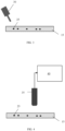
- FIG. 1 shows a structure with damaged portions in accordance with aspects of the present disclosure.
- a photonics structure 10 includes a chip 12 with a grating coupler 20 split into a plurality of waveguide structures 15a, 15b, 15c, 15d ... 15n using a splitter 25 as is known in the art.
- a splitter 25 any number of back-to-back spot size converters, e.g., waveguide structures, are contemplated by the present disclosure.
- the grating coupler 20 may be split from 1 to n waveguide structures and, more preferably 1 to 8 waveguide structures.
- the waveguide structures 15a, 15b, 15c, 15d ... 15n may be embedded with insulator material, e.g., buried oxide, SiO 2 , thermal oxide, TEOS, etc., as represented by reference numeral 12.
- each of the waveguide structures 15a, 15b, 15c, 15d ... 15n may include one or more damaged regions 25.
- the damage regions 25 may be provided in unique patterns for a given wafer/chip so that it can be used as an identification system for photonics chips, as an example.
- the damaged regions 25 may be scattering sites (spots) which are too small to be visible in optical microscopes; instead, in preferred embodiments, the damaged regions 25 are visible in non-visible light (e.g., infrared spectrum).
- FIGS. 2A-2D show different configurations of the waveguide structures 15 that may be implemented in any of the embodiments described herein.
- the waveguide structures 15 may be composed of patterned Si.
- the waveguide structures 15 may be composed of SiN or other dielectric materials, e.g., nitrogen-doped silicon carbide (SiCN), SiO 2 , doped SiO 2 , Si 3 N 4 (SiN), Si, SiON, Al 2 O 3 , AlN, diamond, etc.
- the waveguide structures 15 may be applicable to solid and metamaterial edge couplers, and may include offsets along the longitudinal direction.
- the waveguide structure 15 may include a taper as shown in FIG. 2A or a straight configuration as shown in FIG. 1 .
- the waveguide structure 15 may include stripes or posts 15' (at a taper portion or straight portion).
- the waveguide structure 15 may include partial stripes 15" (which include a spine); whereas, in FIG. 2D , the waveguide structure 15 may include a combination of stripes 15' with partial stripes 15"at the end portions.
- the stripes 15' and the partial stripes 15" may be fully or partially etched features, respectively, of SiN (or other material described herein) of the waveguide structure 15.
- two known scattering sites 25a may be mandated by design.
- the known scattering sites 25a may be a product of a post to spine transition.
- FIG. 3 shows a method of manufacturing the structure shown in FIG. 1 .
- an external laser 30 may be programmed to melt selective areas in the waveguide structure 15 resulting in the damaged regions 25.
- the damaged regions 25 may act as light scattering sites, e.g., scatter incident light, which will encode a wafer ID and the position of the chip within the wafer, as examples.
- the external laser 30 may be provided in different wavelengths depending on the material of the waveguide structure 15. For example, a particular wavelength of the external laser 30 may be used based on the absorption spectrum of the material of the waveguide structure 15 and which wavelength would damage such material. In embodiments, the external laser 30 may be provided in a green wavelength, e.g., about 550 nm.
- FIG. 4 shows a system and method of decoding the identification of the structure 10 shown in FIG. 1 .
- a camera 35 may be used to scan the waveguide structure 15 for damaged regions 25.
- the camera 35 is an infrared camera that can pick up the damaged regions 25, e.g., scattering sites, introduced by the external laser shown in FIG. 3 .
- the images taken by the camera 35 may be fed into a decoder 40.
- the decoder 40 may then decode the positions of the damaged regions 25 and reconcile such with a known pattern configuration for a specific chip to identify the chip. In this way, the position of the damaged regions 25 can be read by the camera 35 to be decoded by the decoder 40 in order to identify a photonics chip (e.g., the wafer and chip position) with no external electrical connections.
- the decoder 40 may be a 1D barcode system when the grating coupler 20 is not split into multiple waveguide structures 15.
- the decoder 40 may be a 2D data matrix system when the grating coupler 20 is split into multiple waveguide structures 15.
- SoC system on chip
- the SoC is an integrated circuit (also known as a "chip") that integrates all components of an electronic system on a single chip or substrate. As the components are integrated on a single substrate, SoCs consume much less power and take up much less area than multichip designs with equivalent functionality. Because of this, SoCs are becoming the dominant force in the mobile computing (such as in Smartphones) and edge computing markets. SoC is also used in embedded systems and the Internet of Things.
- the method(s) as described above is used in the fabrication of integrated circuit chips.
- the resulting integrated circuit chips can be distributed by the fabricator in raw wafer form (that is, as a single wafer that has multiple unpackaged chips), as a bare die, or in a packaged form.
- the chip is mounted in a single chip package (such as a plastic carrier, with leads that are affixed to a motherboard or other higher level carrier) or in a multichip package (such as a ceramic carrier that has either or both surface interconnections or buried interconnections).
- the chip is then integrated with other chips, discrete circuit elements, and/or other signal processing devices as part of either (a) an intermediate product, such as a motherboard, or (b) an end product.
- the end product can be any product that includes integrated circuit chips, ranging from toys and other low-end applications to advanced computer products having a display, a keyboard or other input device, and a central processor.
Landscapes
- Physics & Mathematics (AREA)
- Engineering & Computer Science (AREA)
- Optics & Photonics (AREA)
- General Physics & Mathematics (AREA)
- Microelectronics & Electronic Packaging (AREA)
- Plasma & Fusion (AREA)
- Mechanical Engineering (AREA)
- Optical Integrated Circuits (AREA)
Abstract
Description
- The present disclosure relates to semiconductor structures and, more particularly, to an identification system, method of manufacture and method of use for identifying photonics chips.
- Chip identification can be performed through electrical fuses. With the use of the electrical fuses, probing the chips can be performed electrically, which returns a binary code corresponding to a given wafer and position on the wafer.
- Many silicon photonics chips, though, do not have electrical probing functionalities. Accordingly, there is no existing tracking methods on the dies once these dies are diced up from the wafer. And without any probing, these chips cannot be identified.
- In an aspect of the disclosure, a structure comprises: at least one waveguide structure and at least one damaged region positioned in a unique pattern on the at least one waveguide structure.
- Additional features of the structure are set forth in dependent claims 2 to 8.
- In an aspect of the disclosure, a structure comprises: a grating coupler; at least one waveguide structure optically coupled to the grating coupler, the at least one waveguide structure comprising a spine, posts, and a scattering site at a transition of the spine and the posts; and at least one damaged region positioned in a unique pattern on the at least one waveguide structure.
- Additional features of the structure are set forth in
dependent claims 10 to 11. - In an aspect of the disclosure, a method comprises damaging at least one waveguide structure with a unique pattern for a given photonics chip.
- Additional features of the method are set forth in dependent claims 13 to 15.
- The present disclosure is described in the detailed description which follows, in reference to the noted plurality of drawings by way of non-limiting examples of exemplary embodiments of the present disclosure.
-
FIG. 1 shows a structure with damaged portions in accordance with aspects of the present disclosure. -
FIGS. 2A-2D show different configurations of a waveguide structure that may be implemented in any of the aspects of the present disclosure. -
FIG. 3 shows a method of manufacturing the structure shown inFIG. 1 . -
FIG. 4 shows a system and method of decoding the identification of the structure shown inFIG. 1 . - The present disclosure relates to semiconductor structures and, more particularly, to an identification system, method of manufacture and method of use for identifying photonics chips. More specifically, the present disclosure relates to an infrared identification system for bare dies, method of manufacture and method of use. In embodiments, a chip identification (ID) may be encoded on optical bare dies (e.g., photonics chips) that have no electrical probing capabilities. Advantageously, by implementing the aspects of the present disclosure it is now possible to enable tracking of bare dies after dicing.
- In embodiments, a photonics structure (e.g., grating coupler) may include damaged regions not visible in optical light. The damaged regions, though, may be visible in non-visible light (e.g., infrared). The damaged regions may be formed in unique patterns for a given wafer/chip so that it can be used as an identification system for photonics chips. The damaged portions may be provided by an external laser to selectively induce scattering spots in the device, which are later used to identify the photonics chip. The damage may be read by an infrared camera coupled to a decoding system. In this way, a chip ID may be encoded on photonics chips that have no electrical probing capabilities.
- The photonics structures of the present disclosure can be manufactured in a number of ways using a number of different tools. In general, though, the methodologies and tools are used to form structures with dimensions in the micrometer and nanometer scale. The methodologies, i.e., technologies, employed to manufacture the structures of the present disclosure have been adopted from integrated circuit (IC) technology. For example, the structures are built on wafers and are realized in films of material patterned by photolithographic processes on the top of a wafer. In particular, the fabrication of the structures uses three basic building blocks: (i) deposition of thin films of material on a substrate, (ii) applying a patterned mask on top of the films by photolithographic imaging, and (iii) etching the films selectively to the mask. In addition, precleaning processes may be used to clean etched surfaces of any contaminants, as is known in the art. Moreover, when necessary, rapid thermal anneal processes may be used to drive-in dopants or material layers as is known in the art.
-
FIG. 1 shows a structure with damaged portions in accordance with aspects of the present disclosure. More specifically, aphotonics structure 10 includes achip 12 with agrating coupler 20 split into a plurality ofwaveguide structures splitter 25 as is known in the art. In embodiments, any number of back-to-back spot size converters, e.g., waveguide structures, are contemplated by the present disclosure. For example, thegrating coupler 20 may be split from 1 to n waveguide structures and, more preferably 1 to 8 waveguide structures. Thewaveguide structures reference numeral 12. - As further shown in
FIG. 1 , each of thewaveguide structures regions 25. Thedamage regions 25 may be provided in unique patterns for a given wafer/chip so that it can be used as an identification system for photonics chips, as an example. The damagedregions 25 may be scattering sites (spots) which are too small to be visible in optical microscopes; instead, in preferred embodiments, the damagedregions 25 are visible in non-visible light (e.g., infrared spectrum). -
FIGS. 2A-2D show different configurations of thewaveguide structures 15 that may be implemented in any of the embodiments described herein. It should be understood by those of skill in the art that thewaveguide structures 15 may be composed of patterned Si. For example, thewaveguide structures 15 may be composed of SiN or other dielectric materials, e.g., nitrogen-doped silicon carbide (SiCN), SiO2, doped SiO2, Si3N4 (SiN), Si, SiON, Al2O3, AlN, diamond, etc. Also, thewaveguide structures 15 may be applicable to solid and metamaterial edge couplers, and may include offsets along the longitudinal direction. - For example, the
waveguide structure 15 may include a taper as shown inFIG. 2A or a straight configuration as shown inFIG. 1 . As shown inFIG. 2B , thewaveguide structure 15 may include stripes or posts 15' (at a taper portion or straight portion). InFIG. 2C , thewaveguide structure 15 may includepartial stripes 15" (which include a spine); whereas, inFIG. 2D , thewaveguide structure 15 may include a combination of stripes 15' withpartial stripes 15"at the end portions. In embodiments, and as should be understood by one of skill in the art, the stripes 15' and thepartial stripes 15" may be fully or partially etched features, respectively, of SiN (or other material described herein) of thewaveguide structure 15. Moreover, in the configuration ofFIG. 2D , two knownscattering sites 25a may be mandated by design. For example, the knownscattering sites 25a may be a product of a post to spine transition. -
FIG. 3 shows a method of manufacturing the structure shown inFIG. 1 . In particular, anexternal laser 30 may be programmed to melt selective areas in thewaveguide structure 15 resulting in the damagedregions 25. In embodiments, the damagedregions 25 may act as light scattering sites, e.g., scatter incident light, which will encode a wafer ID and the position of the chip within the wafer, as examples. - The
external laser 30 may be provided in different wavelengths depending on the material of thewaveguide structure 15. For example, a particular wavelength of theexternal laser 30 may be used based on the absorption spectrum of the material of thewaveguide structure 15 and which wavelength would damage such material. In embodiments, theexternal laser 30 may be provided in a green wavelength, e.g., about 550 nm. -
FIG. 4 shows a system and method of decoding the identification of thestructure 10 shown inFIG. 1 . As shown in the system ofFIG. 4 , acamera 35 may be used to scan thewaveguide structure 15 for damagedregions 25. In embodiments, thecamera 35 is an infrared camera that can pick up the damagedregions 25, e.g., scattering sites, introduced by the external laser shown inFIG. 3 . - The images taken by the
camera 35 may be fed into adecoder 40. Thedecoder 40 may then decode the positions of the damagedregions 25 and reconcile such with a known pattern configuration for a specific chip to identify the chip. In this way, the position of the damagedregions 25 can be read by thecamera 35 to be decoded by thedecoder 40 in order to identify a photonics chip (e.g., the wafer and chip position) with no external electrical connections. In embodiments, thedecoder 40 may be a 1D barcode system when thegrating coupler 20 is not split intomultiple waveguide structures 15. Alternatively, thedecoder 40 may be a 2D data matrix system when thegrating coupler 20 is split intomultiple waveguide structures 15. - The structures can be utilized in system on chip (SoC) technology. The SoC is an integrated circuit (also known as a "chip") that integrates all components of an electronic system on a single chip or substrate. As the components are integrated on a single substrate, SoCs consume much less power and take up much less area than multichip designs with equivalent functionality. Because of this, SoCs are becoming the dominant force in the mobile computing (such as in Smartphones) and edge computing markets. SoC is also used in embedded systems and the Internet of Things.
- The method(s) as described above is used in the fabrication of integrated circuit chips. The resulting integrated circuit chips can be distributed by the fabricator in raw wafer form (that is, as a single wafer that has multiple unpackaged chips), as a bare die, or in a packaged form. In the latter case the chip is mounted in a single chip package (such as a plastic carrier, with leads that are affixed to a motherboard or other higher level carrier) or in a multichip package (such as a ceramic carrier that has either or both surface interconnections or buried interconnections). In any case the chip is then integrated with other chips, discrete circuit elements, and/or other signal processing devices as part of either (a) an intermediate product, such as a motherboard, or (b) an end product. The end product can be any product that includes integrated circuit chips, ranging from toys and other low-end applications to advanced computer products having a display, a keyboard or other input device, and a central processor.
- The descriptions of the various embodiments of the present disclosure have been presented for purposes of illustration, but are not intended to be exhaustive or limited to the embodiments disclosed. Many modifications and variations will be apparent to those of ordinary skill in the art without departing from the scope and spirit of the described embodiments. The terminology used herein was chosen to best explain the principles of the embodiments, the practical application or technical improvement over technologies found in the marketplace, or to enable others of ordinary skill in the art to understand the embodiments disclosed herein.
Claims (15)
- A structure comprising at least one waveguide structure and at least one damaged region positioned in a unique pattern on the at least one waveguide structure.
- The structure of claim 1, wherein the at least one damaged region is not visible in optical light or visible in an infrared spectrum.
- The structure of claim 1 or 2, wherein the at least one damage region comprises multiple damaged regions in the unique pattern on the at least one waveguide structure.
- The structure of one of claims 1 to 3, wherein the at least one waveguide structure comprises multiple waveguide structures split from a grating coupler.
- The structure of claim 4, wherein the at least one damaged region comprises multiple damaged regions in the unique pattern on the multiple waveguide structures.
- The structure of one of claims 1 to 5, wherein the at least one waveguide structure comprises a spine.
- The structure of claim 6, wherein the at least one waveguide structure comprises posts transitioning from the spine.
- The structure of claim 7, further comprising light scattering sites at the transition between the posts and the spine, wherein the at least one waveguide structure optionally comprises Si material.
- A structure comprising:a grating coupler;at least one waveguide structure optically coupled to the grating coupler, the at least one waveguide structure comprising a spine, posts, and a light scattering site at a transition of the spine and the posts; andat least one damaged region positioned in a unique pattern on the at least one waveguide structure.
- The structure of claim 9, wherein the at least one damaged region is not visible in optical light or visible in an infrared spectrum.
- The structure of claim 9, wherein the at least one damaged region comprises multiple light scattering sites in the unique pattern or a melted portion of Si material.
- A method comprising damaging at least one waveguide structure with a unique pattern for a given photonics chip.
- The method of claim 12, wherein the damaging comprising melting specific locations on multiple waveguide structures on the given photonics chip.
- The method of claim 13, wherein the damaging is provided by an external laser, wherein the damaging optionally is a light scattering site visible in an infrared spectrum.
- The method of one of claims 12 to 14, further comprising identifying the given photonics chip by scanning the unique pattern with an infrared camera and decoding an image of the unique pattern with a decoder.
Applications Claiming Priority (1)
| Application Number | Priority Date | Filing Date | Title |
|---|---|---|---|
| US18/076,265 US12332480B2 (en) | 2022-12-06 | 2022-12-06 | Identification system |
Publications (3)
| Publication Number | Publication Date |
|---|---|
| EP4382976A1 true EP4382976A1 (en) | 2024-06-12 |
| EP4382976B1 EP4382976B1 (en) | 2026-03-11 |
| EP4382976C0 EP4382976C0 (en) | 2026-03-11 |
Family
ID=88192238
Family Applications (1)
| Application Number | Title | Priority Date | Filing Date |
|---|---|---|---|
| EP23199265.2A Active EP4382976B1 (en) | 2022-12-06 | 2023-09-25 | Identification system |
Country Status (3)
| Country | Link |
|---|---|
| US (1) | US12332480B2 (en) |
| EP (1) | EP4382976B1 (en) |
| CN (1) | CN118151294A (en) |
Citations (6)
| Publication number | Priority date | Publication date | Assignee | Title |
|---|---|---|---|---|
| WO2005011076A1 (en) * | 2003-07-31 | 2005-02-03 | Bookham Technology Plc | Weakly guiding ridge waveguides with vertical gratings |
| WO2014206476A1 (en) * | 2013-06-27 | 2014-12-31 | Das-Nano, S.L. | Optical devices and authentication methods |
| WO2015081436A1 (en) * | 2013-12-03 | 2015-06-11 | Polyvalor, Limited Partnership | Low loss optical waveguides inscribed in media glass substrates, associated optical devices and femtosecond laser-based systems and methods for inscribing the waveguides |
| US20190066543A1 (en) * | 2016-02-25 | 2019-02-28 | Fraunhofer-Gesellschaft Zur Förderung Der Angewand Der Angewandten Forschung E.V. | Seal and Sealing Method |
| US10816726B1 (en) * | 2019-08-23 | 2020-10-27 | Globalfoundries Inc. | Edge couplers for photonics applications |
| US20220252790A1 (en) * | 2021-02-08 | 2022-08-11 | Globalfoundries U.S. Inc. | Hybrid edge couplers with layers in multiple levels |
Family Cites Families (33)
| Publication number | Priority date | Publication date | Assignee | Title |
|---|---|---|---|---|
| US3728521A (en) * | 1970-09-29 | 1973-04-17 | Bliss & Laughlin Ind | Encoded card employing fiber optic elements |
| US4323755A (en) * | 1979-09-24 | 1982-04-06 | Rca Corporation | Method of making a machine-readable marking in a workpiece |
| DE3324551A1 (en) * | 1983-07-07 | 1985-01-17 | Wacker-Chemitronic Gesellschaft für Elektronik-Grundstoffe mbH, 8263 Burghausen | METHOD FOR LABELING SEMICONDUCTOR SURFACES BY LASER RADIATION |
| JPH0834003B2 (en) * | 1990-03-08 | 1996-03-29 | 直弘 丹野 | Optical waveguide storage medium and optical reproducing device |
| US5195163A (en) * | 1991-09-27 | 1993-03-16 | The United States Of America As Represented By The Secretary Of The Navy | Fabrication and phase tuning of an optical waveguide device |
| US5329090A (en) * | 1993-04-09 | 1994-07-12 | A B Lasers, Inc. | Writing on silicon wafers |
| JPH11135390A (en) * | 1997-10-27 | 1999-05-21 | Sony Corp | Wafer on which ID is printed, method for manufacturing semiconductor device, and apparatus for manufacturing semiconductor device |
| GB2338079B (en) * | 1998-06-04 | 2003-02-19 | Bookham Technology Ltd | Optical waveguide attenuation |
| US7104449B2 (en) * | 1998-11-12 | 2006-09-12 | Wenyu Han | Method and apparatus for patterning cards, instruments and documents |
| US7298936B1 (en) * | 2000-12-04 | 2007-11-20 | Graywire Llc | Facile production of optical communication assemblies and components |
| US7315679B2 (en) * | 2004-06-07 | 2008-01-01 | California Institute Of Technology | Segmented waveguide structures |
| US8076776B2 (en) * | 2009-06-16 | 2011-12-13 | Intel Corporation | Integrated circuit package having security feature and method of manufacturing same |
| US8404133B2 (en) * | 2009-08-25 | 2013-03-26 | Fujikura Ltd. | Manufacturing method of planar optical waveguide device with grating structure |
| US8380027B2 (en) * | 2010-05-10 | 2013-02-19 | Intel Corporation | Erasable ion implanted optical couplers |
| GB201009810D0 (en) * | 2010-06-11 | 2010-07-21 | Univ Heriot Watt | A method of forming an optical device |
| US9244000B2 (en) * | 2010-07-07 | 2016-01-26 | Agamatrix, Inc. | Analyte test strip and analyte meter device |
| CN103503003A (en) | 2010-09-08 | 2014-01-08 | 比尔凯科技新加坡有限公司 | An integrated unit for reading identification information based on inherent disorder |
| US9091827B2 (en) * | 2012-07-09 | 2015-07-28 | Luxtera, Inc. | Method and system for grating couplers incorporating perturbed waveguides |
| US8742599B2 (en) | 2012-08-30 | 2014-06-03 | Freescale Semiconductor, Inc. | Identification mechanism for semiconductor device die |
| US9234854B2 (en) | 2013-03-15 | 2016-01-12 | International Business Machines Corporation | Single fiber noncritical-alignment wafer-scale optical testing |
| DE102013219591A1 (en) * | 2013-09-27 | 2015-04-16 | Albert-Ludwigs-Universität Freiburg | METHOD FOR AUTHENTICATING MICROELECTRONIC COMPONENTS |
| KR102255303B1 (en) * | 2014-10-13 | 2021-05-24 | 삼성전자주식회사 | Authentication structure and method for authenticating object and device adopting the same |
| US10740493B2 (en) * | 2015-03-09 | 2020-08-11 | Massachusetts Institute Of Technology | Phosphor-loaded waveguide |
| US10215918B2 (en) * | 2015-11-24 | 2019-02-26 | Omega Optics, Inc. | Subwavelength photonic crystal waveguide in optical systems |
| US9899332B2 (en) * | 2016-02-18 | 2018-02-20 | Texas Instruments Incorporated | Visual identification of semiconductor dies |
| WO2017177105A1 (en) * | 2016-04-07 | 2017-10-12 | The Johns Hopkins University | System and method for physical one-way function authentication via chaotic integrated photonic resonators |
| DE102016109720B4 (en) * | 2016-05-25 | 2023-06-22 | Infineon Technologies Ag | Method of forming a semiconductor device and semiconductor device |
| CN114981699A (en) * | 2019-11-18 | 2022-08-30 | 丹麦科技大学 | In-plane chip scale photonic device |
| US12352568B2 (en) * | 2020-06-23 | 2025-07-08 | Clemson University Research Foundation | Physical unclonable function from an integrated photonic interferometer |
| EP3933469A1 (en) * | 2020-07-03 | 2022-01-05 | LightOn | Integrated photonic mixing devices and optical computing systems including such devices |
| US11501097B2 (en) * | 2020-09-15 | 2022-11-15 | Government Of The United States Of America, As Represented By The Secretary Of Commerce | Barcoded end facet printed photonic chip and barcode-guided direct laser writing |
| US11409040B1 (en) * | 2021-03-23 | 2022-08-09 | Globalfoundries U.S. Inc. | Optical couplers for ridge-to-rib waveguide core transitions |
| EP4166497A1 (en) * | 2021-10-15 | 2023-04-19 | Schott Ag | Enclosure with information pattern |
-
2022
- 2022-12-06 US US18/076,265 patent/US12332480B2/en active Active
-
2023
- 2023-09-25 EP EP23199265.2A patent/EP4382976B1/en active Active
- 2023-10-27 CN CN202311418470.5A patent/CN118151294A/en active Pending
Patent Citations (6)
| Publication number | Priority date | Publication date | Assignee | Title |
|---|---|---|---|---|
| WO2005011076A1 (en) * | 2003-07-31 | 2005-02-03 | Bookham Technology Plc | Weakly guiding ridge waveguides with vertical gratings |
| WO2014206476A1 (en) * | 2013-06-27 | 2014-12-31 | Das-Nano, S.L. | Optical devices and authentication methods |
| WO2015081436A1 (en) * | 2013-12-03 | 2015-06-11 | Polyvalor, Limited Partnership | Low loss optical waveguides inscribed in media glass substrates, associated optical devices and femtosecond laser-based systems and methods for inscribing the waveguides |
| US20190066543A1 (en) * | 2016-02-25 | 2019-02-28 | Fraunhofer-Gesellschaft Zur Förderung Der Angewand Der Angewandten Forschung E.V. | Seal and Sealing Method |
| US10816726B1 (en) * | 2019-08-23 | 2020-10-27 | Globalfoundries Inc. | Edge couplers for photonics applications |
| US20220252790A1 (en) * | 2021-02-08 | 2022-08-11 | Globalfoundries U.S. Inc. | Hybrid edge couplers with layers in multiple levels |
Also Published As
| Publication number | Publication date |
|---|---|
| US20240184045A1 (en) | 2024-06-06 |
| US12332480B2 (en) | 2025-06-17 |
| EP4382976B1 (en) | 2026-03-11 |
| EP4382976C0 (en) | 2026-03-11 |
| CN118151294A (en) | 2024-06-07 |
Similar Documents
| Publication | Publication Date | Title |
|---|---|---|
| US10509174B2 (en) | Photonic integration platform | |
| US10877229B2 (en) | Edge coupling through unetched surface of photonic chip | |
| US12512402B2 (en) | Chip-last wafer-level fan-out with optical fiber alignment structure | |
| US20240210628A1 (en) | Devices, systems, and methods for optical signal processing | |
| US12019286B2 (en) | Optical edge coupler having a heterogeneous cladding structure | |
| US10585219B2 (en) | Grating couplers with multiple configurations | |
| US10690845B1 (en) | Three dimensional optical interconnects | |
| US10649138B2 (en) | Optical device having a photonic chip with one or more suspended functional portions | |
| Fedeli et al. | Integration issues of a photonic layer on top of a CMOS circuit | |
| US12332480B2 (en) | Identification system | |
| US10241269B1 (en) | Grating couplers with multiple configurations | |
| JP2007524991A (en) | Semiconductor alignment aid | |
| US11353651B2 (en) | Multi-mode optical waveguide structures with isolated absorbers | |
| CN115113326B (en) | Optical coupler for ridge-to-rib waveguide core transition | |
| US11101617B2 (en) | Wafer-level handle replacement | |
| US10746907B2 (en) | Grating couplers with cladding layer(s) | |
| Roelkens et al. | Coupling schemes for heterogeneous integration of III-V membrane devices and silicon-on-insulator waveguides | |
| US20170068052A1 (en) | Frontside coupled waveguide with backside optical connection | |
| US12078845B2 (en) | Optical system | |
| US11409046B2 (en) | Backside binary grated lens coupled to front side waveguide | |
| US20040245538A1 (en) | Double sided optoelectronic integrated circuit | |
| Dannberg et al. | Integration of optical interconnects and optoelectronic elements on wafer-scale | |
| JPH05249340A (en) | Optical component coupling device | |
| KR20000046923A (en) | Method for manufacturing laser diode chip for optical communication |
Legal Events
| Date | Code | Title | Description |
|---|---|---|---|
| PUAI | Public reference made under article 153(3) epc to a published international application that has entered the european phase |
Free format text: ORIGINAL CODE: 0009012 |
|
| STAA | Information on the status of an ep patent application or granted ep patent |
Free format text: STATUS: THE APPLICATION HAS BEEN PUBLISHED |
|
| AK | Designated contracting states |
Kind code of ref document: A1 Designated state(s): AL AT BE BG CH CY CZ DE DK EE ES FI FR GB GR HR HU IE IS IT LI LT LU LV MC ME MK MT NL NO PL PT RO RS SE SI SK SM TR |
|
| STAA | Information on the status of an ep patent application or granted ep patent |
Free format text: STATUS: REQUEST FOR EXAMINATION WAS MADE |
|
| 17P | Request for examination filed |
Effective date: 20240710 |
|
| RBV | Designated contracting states (corrected) |
Designated state(s): AL AT BE BG CH CY CZ DE DK EE ES FI FR GB GR HR HU IE IS IT LI LT LU LV MC ME MK MT NL NO PL PT RO RS SE SI SK SM TR |
|
| GRAP | Despatch of communication of intention to grant a patent |
Free format text: ORIGINAL CODE: EPIDOSNIGR1 |
|
| STAA | Information on the status of an ep patent application or granted ep patent |
Free format text: STATUS: GRANT OF PATENT IS INTENDED |
|
| INTG | Intention to grant announced |
Effective date: 20251212 |
|
| GRAS | Grant fee paid |
Free format text: ORIGINAL CODE: EPIDOSNIGR3 |
|
| GRAA | (expected) grant |
Free format text: ORIGINAL CODE: 0009210 |
|
| STAA | Information on the status of an ep patent application or granted ep patent |
Free format text: STATUS: THE PATENT HAS BEEN GRANTED |
|
| AK | Designated contracting states |
Kind code of ref document: B1 Designated state(s): AL AT BE BG CH CY CZ DE DK EE ES FI FR GB GR HR HU IE IS IT LI LT LU LV MC ME MK MT NL NO PL PT RO RS SE SI SK SM TR |
|
| REG | Reference to a national code |
Ref country code: CH Ref legal event code: F10 Free format text: ST27 STATUS EVENT CODE: U-0-0-F10-F00 (AS PROVIDED BY THE NATIONAL OFFICE) Effective date: 20260311 Ref country code: GB Ref legal event code: FG4D |
|
| REG | Reference to a national code |
Ref country code: IE Ref legal event code: FG4D |
|
| U01 | Request for unitary effect filed |
Effective date: 20260311 |
|
| U07 | Unitary effect registered |
Designated state(s): AT BE BG DE DK EE FI FR IT LT LU LV MT NL PT RO SE SI Effective date: 20260316 |
|
| PG25 | Lapsed in a contracting state [announced via postgrant information from national office to epo] |
Ref country code: RS Free format text: LAPSE BECAUSE OF FAILURE TO SUBMIT A TRANSLATION OF THE DESCRIPTION OR TO PAY THE FEE WITHIN THE PRESCRIBED TIME-LIMIT Effective date: 20260611 |
|
| PG25 | Lapsed in a contracting state [announced via postgrant information from national office to epo] |
Ref country code: ES Free format text: LAPSE BECAUSE OF FAILURE TO SUBMIT A TRANSLATION OF THE DESCRIPTION OR TO PAY THE FEE WITHIN THE PRESCRIBED TIME-LIMIT Effective date: 20260311 |
|
| PG25 | Lapsed in a contracting state [announced via postgrant information from national office to epo] |
Ref country code: GR Free format text: LAPSE BECAUSE OF FAILURE TO SUBMIT A TRANSLATION OF THE DESCRIPTION OR TO PAY THE FEE WITHIN THE PRESCRIBED TIME-LIMIT Effective date: 20260612 |
|
| PG25 | Lapsed in a contracting state [announced via postgrant information from national office to epo] |
Ref country code: NO Free format text: LAPSE BECAUSE OF FAILURE TO SUBMIT A TRANSLATION OF THE DESCRIPTION OR TO PAY THE FEE WITHIN THE PRESCRIBED TIME-LIMIT Effective date: 20260611 |
|
| PG25 | Lapsed in a contracting state [announced via postgrant information from national office to epo] |
Ref country code: HR Free format text: LAPSE BECAUSE OF FAILURE TO SUBMIT A TRANSLATION OF THE DESCRIPTION OR TO PAY THE FEE WITHIN THE PRESCRIBED TIME-LIMIT Effective date: 20260311 |