EP4382869A1 - Sensor readout system and sensor readout method - Google Patents
Sensor readout system and sensor readout method Download PDFInfo
- Publication number
- EP4382869A1 EP4382869A1 EP22212170.9A EP22212170A EP4382869A1 EP 4382869 A1 EP4382869 A1 EP 4382869A1 EP 22212170 A EP22212170 A EP 22212170A EP 4382869 A1 EP4382869 A1 EP 4382869A1
- Authority
- EP
- European Patent Office
- Prior art keywords
- signal
- chop
- biasing
- sensor
- generate
- Prior art date
- Legal status (The legal status is an assumption and is not a legal conclusion. Google has not performed a legal analysis and makes no representation as to the accuracy of the status listed.)
- Pending
Links
Images



Classifications
-
- G—PHYSICS
- G01—MEASURING; TESTING
- G01D—MEASURING NOT SPECIALLY ADAPTED FOR A SPECIFIC VARIABLE; ARRANGEMENTS FOR MEASURING TWO OR MORE VARIABLES NOT COVERED IN A SINGLE OTHER SUBCLASS; TARIFF METERING APPARATUS; MEASURING OR TESTING NOT OTHERWISE PROVIDED FOR
- G01D3/00—Indicating or recording apparatus with provision for the special purposes referred to in the subgroups
- G01D3/028—Indicating or recording apparatus with provision for the special purposes referred to in the subgroups mitigating undesired influences, e.g. temperature, pressure
- G01D3/036—Indicating or recording apparatus with provision for the special purposes referred to in the subgroups mitigating undesired influences, e.g. temperature, pressure on measuring arrangements themselves
-
- G—PHYSICS
- G01—MEASURING; TESTING
- G01D—MEASURING NOT SPECIALLY ADAPTED FOR A SPECIFIC VARIABLE; ARRANGEMENTS FOR MEASURING TWO OR MORE VARIABLES NOT COVERED IN A SINGLE OTHER SUBCLASS; TARIFF METERING APPARATUS; MEASURING OR TESTING NOT OTHERWISE PROVIDED FOR
- G01D5/00—Mechanical means for transferring the output of a sensing member; Means for converting the output of a sensing member to another variable where the form or nature of the sensing member does not constrain the means for converting; Transducers not specially adapted for a specific variable
- G01D5/12—Mechanical means for transferring the output of a sensing member; Means for converting the output of a sensing member to another variable where the form or nature of the sensing member does not constrain the means for converting; Transducers not specially adapted for a specific variable using electric or magnetic means
- G01D5/14—Mechanical means for transferring the output of a sensing member; Means for converting the output of a sensing member to another variable where the form or nature of the sensing member does not constrain the means for converting; Transducers not specially adapted for a specific variable using electric or magnetic means influencing the magnitude of a current or voltage
- G01D5/16—Mechanical means for transferring the output of a sensing member; Means for converting the output of a sensing member to another variable where the form or nature of the sensing member does not constrain the means for converting; Transducers not specially adapted for a specific variable using electric or magnetic means influencing the magnitude of a current or voltage by varying resistance
-
- G—PHYSICS
- G01—MEASURING; TESTING
- G01R—MEASURING ELECTRIC VARIABLES; MEASURING MAGNETIC VARIABLES
- G01R17/00—Measuring arrangements involving comparison with a reference value, e.g. bridge
- G01R17/10—AC or DC measuring bridges
- G01R17/105—AC or DC measuring bridges for measuring impedance or resistance
-
- G—PHYSICS
- G01—MEASURING; TESTING
- G01R—MEASURING ELECTRIC VARIABLES; MEASURING MAGNETIC VARIABLES
- G01R33/00—Arrangements or instruments for measuring magnetic variables
- G01R33/0023—Electronic aspects, e.g. circuits for stimulation, evaluation, control; Treating the measured signals; calibration
- G01R33/0029—Treating the measured signals, e.g. removing offset or noise
-
- H—ELECTRICITY
- H03—ELECTRONIC CIRCUITRY
- H03F—AMPLIFIERS
- H03F3/00—Amplifiers with only discharge tubes or only semiconductor devices as amplifying elements
- H03F3/38—DC amplifiers with modulator at input and demodulator at output; Modulators or demodulators specially adapted for use in such amplifiers
-
- H—ELECTRICITY
- H03—ELECTRONIC CIRCUITRY
- H03M—CODING; DECODING; CODE CONVERSION IN GENERAL
- H03M1/00—Analogue/digital conversion; Digital/analogue conversion
- H03M1/06—Continuously compensating for, or preventing, undesired influence of physical parameters
- H03M1/0617—Continuously compensating for, or preventing, undesired influence of physical parameters characterised by the use of methods or means not specific to a particular type of detrimental influence
- H03M1/0626—Continuously compensating for, or preventing, undesired influence of physical parameters characterised by the use of methods or means not specific to a particular type of detrimental influence by filtering
- H03M1/0629—Anti-aliasing
-
- H—ELECTRICITY
- H03—ELECTRONIC CIRCUITRY
- H03F—AMPLIFIERS
- H03F2200/00—Indexing scheme relating to amplifiers
- H03F2200/261—Amplifier which being suitable for instrumentation applications
Definitions
- the invention relates to sensor readout channels, especially to Wheatstone bridge based sensor readout channels for reading out impedance sensors.
- Wheatstone bridges are widely used to read out impedance sensors that may monitor physical parameters such as temperature, pressure, humidity, etc., and of which their output may be digitized by readout channels.
- a readout channel may comprise an instrumentation amplifier (IA) to amplify the weak sensor signal and an analog-to-digital converter (ADC) for domain conversion.
- IA instrumentation amplifier
- ADC analog-to-digital converter
- a chopper-based stabilization of the IA may be performed to reduce the input direct current (DC) offset and low-frequency input noise that may degrade the performance of precision DC IAs.
- the sensor signal may be first multiplied by a chopping signal, then may be amplified and may be multiplied again by a similar switching function, and finally may be low-pass filtered.
- the first multiplication may translate the sensor signal spectrum into the high-frequency (HF) region and the second multiplication may recover the amplified original signal by demodulating the signal back to the baseband.
- the input-referred amplifier DC offset and low-frequency noise components may only go through the second multiplication process, and thus the DC offset may be converted into an HF component at the output and may be fully attenuated by the low-pass filter (LPF).
- LPF low-pass filter
- the LPF may require a low cut-off frequency and therefore may require an appreciable silicon area.
- the above-mentioned chopper stabilization can be implemented in the channel for both the IA and the ADC.
- a bulky LPF may be needed, especially before the signal can be sampled by the ADC.
- a buffer or a programmable gain amplifier (PGA) may be needed in front of the ADC, which may add additional power consumption to the channel.
- an object of the invention is to facilitate Wheatstone bridge based sensor readout channels that are robust to the channel generated noise, and to stabilize the IA in the sensing channel to allow a more relaxed low-pass filtration (i.e., size constrain) and further to reduce the overall power consumption, and moreover to improve the gain accuracy of the filtered signal.
- the object is solved by the features of the first independent claim for the sensor readout system and by the features of the second independent claim for the sensor readout method.
- the dependent claims contain further developments.
- a sensor readout system comprises a signal generator configured to generate a biasing signal, a first chopper configured to modulate the biasing signal using a chopping signal with a chopping frequency f chop to generate a modulated biasing signal, a Wheatstone bridge circuit comprising resistive branches, at least one of the resistive branches comprises an impedance-based sensor, the Wheatstone bridge circuit being configured to receive the modulated biasing signal and to generate a sensing signal based on the modulated biasing signal, and a second chopper configured to modulate the sensing signal using the chopping signal with the chopping frequency f chop to generate a modulated sensing signal.
- the sensor readout system further comprises an amplifier configured to amplify the modulated sensing signal to generate an amplified signal, a low-pass filter configured to filter the amplified signal with a cutoff frequency of at least 3 ⁇ f chop , preferably a cutoff frequency of 3.5 ⁇ f chop , to generate a filtered signal, an analog-to-digital converter configured to sub-sample the filtered signal with a sampling frequency of N ⁇ 2 ⁇ f chop , where N is an integer, and a correlated double sampling block configured to perform correlated double sampling operation by subtracting the samples at the chopping frequency f chop .
- an amplifier configured to amplify the modulated sensing signal to generate an amplified signal
- a low-pass filter configured to filter the amplified signal with a cutoff frequency of at least 3 ⁇ f chop , preferably a cutoff frequency of 3.5 ⁇ f chop , to generate a filtered signal
- an analog-to-digital converter configured to sub-sample the filtered signal with a sampling frequency
- the low-pass filter may be configured to filter the amplified signal with a cutoff frequency lower than 3 ⁇ f chop , for example, a cutoff frequency of 2.5 ⁇ f chop , to generate the filtered signal.
- the correlated double sampling operation may correspond to a discrete time signal processing technique that may receive or select two samples, especially two opposite or phase-shifted samples, after the sub-sampling operation and may subtract the samples.
- the subtraction may eliminate the input-referred amplifier DC offset and/or low-frequency noise components, while the useful signal component may be doubled in amplitude.
- the first modulation at the first chopper may up-convert any noise components within or associated with the biasing signal to the chopping frequency.
- the chopping signal may be generated and provided by a chopping signal generator, which may generate a square wave of frequency f chop as the chopping signal.
- the second modulation at the second chopper may up-convert the sensor signal from the Wheatstone bridge circuit to the chopping frequency.
- the second chopper may down-convert the up-converted noise components of the biasing signal to the baseband or DC, whereby input-referred amplifier DC offset and low-frequency noise components may also remain at the baseband or DC.
- all noise components at the output of the second chopper and/or the amplifier may remain at the baseband or DC, while the useful signal is up-converted to the chopping frequency in the frequency spectrum.
- the de-modulation may be performed by sub-sampling and further by a correlated double sampling by subtracting the samples, especially to facilitate filtering at or around the chopping frequency to extract the useful signal and to eliminate the noise components, e.g., high-pass filtering at or around the chopping frequency to filter out the noise components at the baseband or DC.
- the low-pass filtering of the amplified signal to include one or more harmonics may improve the gain accuracy, especially by sub-sampling the chopping harmonics.
- the chopping harmonics i.e., the chopping harmonics
- at least one higher order chopping harmonic e.g., one higher order odd harmonic because of the square wave chopping signal, may be filtered along with the up-modulated signal at the chopping frequency which may improve the gain accuracy of the signal and further may decrease the noise components due to sub-sampling of the signals and the noise components.
- a low-pass filtering with a cutoff frequency of 3 ⁇ f chop may reduce the noise but give a higher gain error, whereas a low-pass filtering with a cutoff frequency of 4 ⁇ f chop may give a lower gain error but more noise.
- the low-pass filter cutoff frequency may be defined based on the gain accuracy requirements.
- the low-pass filtering of the amplified signal may not include signal harmonics, i.e., low-pass filtering with a cutoff frequency lower than 3 ⁇ f chop , which may increase the gain error.
- the strict requirements, e.g., the low cut-off, for the low-pass filtration may be relaxed to facilitate compact filters as well as to eliminate the necessity of having buffers and/or PGAs before the analog-to-digital signal conversion.
- the sensor readout system further comprises a multiplexer configured to select the impedance-based sensor from a plurality of impedance-based sensors and further to couple the impedance-based sensor to the at least one of the preferably four resistive branches.
- the multiplexer is further configured to select a reference resistive element having a pre-defined resistance value and further to couple the reference resistive element to the at least one of the four resistive branches.
- At least one of the preferably four resistive branches comprises a variable resistive element.
- at least two of the preferably four resistive branches may comprise a variable resistive element.
- each of the four resistive branches may comprise a variable resistive element.
- the signal generator is configured to generate a biasing current as the biasing signal.
- the signal generator is configured to generate a biasing voltage as the biasing signal.
- the signal generator comprises or is a proportional to absolute temperature (PTAT) bias generator.
- the signal generator may comprise or be a complementary to absolute temperature (CTAT) bias generator. Further alternatively, the signal generator may configure the temperature dependency of the biasing signal.
- the low-pass filter is configured to settle before the sub-sampling of the filtered signal.
- the low-pass filter may reduce or eliminate aliasing effects in the filtered signal.
- the correlated double sampling block is further configured to add a gain factor in digital domain after performing the correlated double sampling operation.
- the gain accuracy can be further improved.
- the correlated double sampling block may apply sinc filtering and/or zero-order-hold to the samples before and/or after the correlated double sampling operation.
- the correlated double sampling block may attenuate the samples by a sinc filter and/or by a zero-order hold model based on the sampling frequency of the analog-to-digital converter to reconstruct the original signal.
- the impedance-based sensor is a resistive temperature sensor or a resistive humidity sensor or a resistive pressure sensor or a Piezoresistive sensor.
- a sensor readout method comprises the steps of generating a biasing signal, modulating the biasing signal using a chopping signal with a chopping frequency f chop to generate a modulated biasing signal, receiving the modulated biasing signal and generating a sensing signal based on the modulated biasing signal by a Wheatstone bridge circuit comprising resistive branches, whereby at least one of the resistive branches comprises an impedance-based sensor, and modulating the sensing signal using the chopping signal with the chopping frequency f chop to generate a modulated sensing signal.
- the method further comprises the steps of amplifying the modulated sensing signal to generate an amplified signal, low-pass filtering the amplified signal with a cutoff frequency of at least 3 ⁇ f chop , preferably a cutoff frequency of 3.5 ⁇ f chop , to generate a filtered signal, sub-sampling the filtered signal with a sampling frequency of N ⁇ 2 ⁇ f chop , where N is an integer, and performing correlated double sampling operation by subtracting the samples at the chopping frequency f chop .
- the low-pass filter may be configured to filter the amplified signal with a cutoff frequency lower than 3 ⁇ f chop , for example, a cutoff frequency of 2.5 ⁇ f chop , to generate the filtered signal.
- the method further comprises the steps of selecting the impedance-based sensor from a plurality of impedance-based sensors, and coupling the impedance-based sensor to the at least one of the preferably four resistive branches.
- the method further comprises the steps of selecting a reference resistive element having a pre-defined resistance value, and coupling the reference resistive element to the at least one of the preferably four resistive branches.
- the method further comprises the step of generating a biasing current as the biasing signal.
- the method further comprises the step of generate a biasing voltage as the biasing signal.
- the method according to the second aspect corresponds to the system according to the first aspect and its implementation forms. Accordingly, the method according to the second aspect achieves the same advantages and effects as the system of the first aspect and its respective implementation forms.
- the system 100 may comprise a signal generator (SG) 101 that may generate a biasing signal 102.
- the signal generator 101 may introduce DC offset and/or low-frequency noise components, hereinafter referred as biasing noise components, in the biasing signal 102.
- the noise signal introduced by the signal generator 101 may remain at the baseband or at DC in the frequency spectrum.
- the system 100 may further comprise a first chopper (CHI) 103 operably coupled to the signal generator 101.
- the first chopper 103 may receive the biasing signal 102 from the signal generator 101 and may modulate the biasing signal 102 using a chopping signal 117 with a chopping frequency f chop to generate a modulated biasing signal 104.
- CHI first chopper
- the system 100 may further comprise a Wheatstone bridge circuit (WB) 105 operably coupled to the first chopper 103.
- the Wheatstone bridge circuit 105 may comprise one or more impedance-based sensors.
- the Wheatstone bridge circuit 105 may receive the modulated biasing signal 104 from the first chopper 103 for biasing the circuitry and may accordingly generate a sensing signal 106, especially an analog measurement signal, e.g., as a result of the measurements carried out by the one or more impedance-based sensors.
- the system 100 may further comprise a second chopper (CH2) 107 operably coupled to the Wheatstone bridge circuit 105.
- the second chopper 107 may receive the sensing signal 106 from the Wheatstone bridge circuit 105, and may modulate the sensing signal 106 using the chopping signal 117 with the chopping frequency f chop to generate a modulated sensing signal 108.
- the term "chopper” should be understood as a multiplier or a modulator that may multiply or mix an input signal with a carrier signal in order to up-modulate or to shift the input signal from the baseband to the frequency of the carrier signal in the frequency spectrum including the generation of corresponding signal harmonics, e.g., due to the modulation with a square wave chopping signal.
- the system 100 may further comprise an amplifier (AMP) 109, especially an instrumentation amplifier (IA), operably coupled to the second chopper 107.
- the amplifier 109 may receive the modulated sensing signal 108 from the second chopper 107, especially at one or more inputs of the amplifier 109, and may amplify the modulated sensing signal 108 to generate an amplified signal 110.
- the amplifier 109 may be a band-limited amplifier having a bandwidth of about 35 ⁇ f chop .
- the amplifier 204 may be designed to have a bandwidth based on the gain accuracy requirements, e.g., a bandwidth lower than 35 ⁇ f chop that may increase the gain error.
- the amplifier 109 may introduce input-referred amplifier DC offset and low-frequency noise components, hereinafter referred as amplifier noise components, while amplifying the modulated sensing signal 108.
- the noise signal introduced by the amplifier 109 may remain at the baseband or at DC in the frequency spectrum.
- the system 100 may further comprise a low-pass filter (LPF) 111 operably coupled to the amplifier 109.
- the LPF 111 may receive the amplified signal 110 from the amplifier 109, and may filter the amplified signal 110 to generate a filtered signal 112.
- the LPF 111 may have a cut-off frequency of about 3.5 ⁇ f chop .
- the filtered signal 112 may comprise one or more harmonic components or chopping harmonics in the frequency spectrum resulted from, e.g., the second chopping operation.
- the chopping signal 117 may be a square wave of frequency f chop .
- the first chopping operation at the first chopper 103 may up-modulate the biasing noise components at the chopping frequency f chop .
- the second chopping operation at the second chopper 107 may up-modulate the sensing signal 106 at the chopping frequency f chop , while at the same time, may down-modulate the biasing noise components at the baseband or DC in the frequency spectrum.
- the modulated sensing signal 108 generated by the second chopper 107 may comprise the sensing signal 106 at the chopping frequency f chop , a first (odd) harmonic component at the frequency 3 ⁇ f chop , a second (odd) harmonic component at the frequency 5 ⁇ f chop and so on in the frequency spectrum.
- the LPF 111 may filter the amplified signal 110 with a cut-off frequency of about 3.5 ⁇ f chop
- the filtered signal 112 may comprise the biasing noise components and the amplifier noise components at the baseband, the sensing signal 108 at the chopping frequency f chop , and the harmonic component at the frequency 3 ⁇ f chop .
- the system may further comprise an analog-to-digital converter (ADC) 113 operably coupled to the LPF 111.
- the ADC 113 may receive the filtered signal 112 from the LPF 111, and may perform sub-sampling of the filtered signal 112 to generate discrete samples 114.
- the ADC 113 may sub-sample the filtered signal 112 with a sampling frequency of N ⁇ 2 ⁇ f chop , e.g., with a sampling frequency of 2 ⁇ f chop for sampling twice during one chopping period T chop .
- the system may further comprise a correlated double sampling (CDS) block 115 operably coupled to the ADC 114.
- the CDS block 115 may operate at the chopping frequency f chop , may receive the samples 114 from the ADC 113, and may perform correlated double sampling operation by subtracting the samples 114 at the chopping frequency f chop .
- the ADC 113 may provide two samples corresponding to two opposite signal level instances or successive levels.
- the CDS block 115 may subtract the samples, which may eliminate or reduce the noise components, however, the useful signal may be doubled in amplitude.
- the system may further comprise a chopping signal generator (CSG) 116 operably coupled to the first chopper 103, the second chopper 107, the ADC 113, and the CDS block 115.
- the chopping signal generator 116 may generate the chopping signal 117 and may provide the chopping signal 117 to the first chopper 103 and to the second chopper 107.
- the signal generator 116 may further generate the sampling clock 118 for the sub-sampling and may provide the sampling clock 118 to the ADC 113.
- the signal generator may further provide the chopping signal 117 as the CDS clock to the CDS block 115.
- the coupling between the above-mentioned entities may correspond to a single-ended connection or a differential connection.
- the signal generator 101 may correspond to a biasing current signal generator.
- the signal generator may comprise a reference current branch (REF) corresponding to the reference current I REF , a PTAT branch corresponding to the I PTAT current as a mirrored or copied version of the I REF , and a CTAT branch corresponding to the I CTAT current as a mirrored or copied version of the I REF .
- REF reference current branch
- PTAT branch corresponding to the I PTAT current as a mirrored or copied version of the I REF
- CTAT branch corresponding to the I CTAT current as a mirrored or copied version of the I REF .
- the REF branch may comprise a PFET M4 and an NFET M1
- the PTAT branch may comprise a PFET M3 and an NFET M2 that may act as current mirrors
- the CTAT branch may comprise a PFET M5 and an NFET M6 that may also act as current mirrors.
- the PTAT branch may comprise a feedback resistor or conductor or element R that may have a positive temperature coefficient.
- the CTAT branch may comprise a further NFET M7 that may have a negative temperature coefficient.
- the opposite temperature coefficients may compensate each other, i.e., if the I PTAT and the I CTAT currents may be set to be roughly equal or may be set in a pre-defined ratio, e.g., a ratio of 10 to 1, at some nominal temperature, the resultant current of the I PTAT and the I CTAT currents may become almost temperature independent.
- the I PTAT and the I CTAT currents may be varied in order to achieve a desired temperature dependency of the resulting biasing current.
- the Wheatstone bridge circuit 105 may comprise a first resistive branch or resistor R1, a second resistive branch or resistor R2, a third resistive branch or resistor R3, and a fourth resistive branch or resistor R4. So the Wheatstone bridge preferably has four resistive branches. It might also have another number of branches, especially an odd number of branches such as six or eight, especially with the same number of branches such as two, three or four, on each side.
- the branches or the resistors R1, R2, R3, R4 may be arranged such that a first node 301 may be formed between R1 and R3, a second node 302 may be formed between R2 and R4, a third node 303 may be formed between R1 and R2, and a fourth node 304 may be formed between R3 and R4.
- at least of the resistors R1, R2, R3, R4 may comprise or be an impedance-based sensor or resistive sensor.
- R1 is illustrated as the impedance-based sensor.
- the resistors R1, R2, R3, R4 each may comprise or be the impedance-based sensor.
- the nodes 303 and 304 may be used for biasing the Wheatstone bridge circuit 105, i.e., may be coupled to the first chopper 103, and the nodes 301 and 302 may be used to readout the measurements from the impedance-based sensor or sensors, i.e., may be coupled to the second chopper 107.
- a second exemplary embodiment of the Wheatstone bridge circuit 105 is illustrated.
- the second exemplary embodiment of Fig. 3B differs from the first exemplary embodiment of Fig. 3A in that at least one resistive branch or resistor may be replaced with a multiplexer 305.
- R1 is replaced with the multiplexer 305.
- the multiplexer 305 may be further coupled to one or more impedance-based sensors, exemplarily three impedance-based sensors Rs1, Rs2, Rs3, and may be further coupled to a reference resistor or sensor Rref.
- the reference resistor Rref may be used to calibrate the Wheatstone bridge circuit 105 and/or to generate reference measurements for calibration of the Wheatstone bridge circuit 105.
- a control 306 may be provided to the multiplexer 305 in order to select the sensors Rref, Rs1, Rs2, and Rs3, e.g., to replace R1 of Fig. 3A .
- the multiplexer 305 can be used to replace any of the resistors R1, R2, R3, R4 in order to select the impedance-based resistor and further to modify the readout path within the Wheatstone bridge circuit 105. Additionally or alternatively, more than one resistors R1, R2, R3, R4 can be replaced using the above-described arrangement so that more than one impedance-based sensor can be used.
- the CDS block 115 may comprise a first decimation block 401 that may receive the ADC samples 114 with a sampling frequency of N ⁇ 2 ⁇ f chop and may decimate or down-sample the samples 114 by N samples, thereby resulting the decimated samples 402 at a sampling frequency of 2 ⁇ f chop .
- the first decimation block 401 may perform a zero-order hold operation or sinc filtering to attenuate the ADC samples 114.
- the CDS block 115 may further comprise a subtraction block 403 operably coupled to the first decimation block 401.
- the subtraction block 403 may operate at the chopping frequency f chop , may receive the decimated samples 402 from the first decimation block 401, and may subtract the samples 402 at the chopping frequency f chop to generate subtracted samples 404.
- the CDS block 115 may further comprise a second decimation block 405 operably coupled to the subtraction block 403.
- the second decimation block 405 may receive the subtracted samples 404 and may decimate or down-sample the samples 404 by 2 samples, thereby resulting the further decimated samples 406 at a sampling frequency of f chop .
- the second decimation block 405 may perform a zero-order hold operation or sinc filtering to attenuate the subtracted samples 404.
- the CDS block 115 may further comprise a third decimation block 407 operably coupled to the second decimation block 405.
- the third decimation block 407 may receive the further decimated samples 406 and may decimate or down-sample the samples 406 to generate the output discrete signal 408 at a suitable frequency, e.g., 40 Hz.
- the third decimation block 407 may perform a zero-order hold operation or sinc filtering to attenuate the further decimated samples 406.
- the CDS block 115 may additionally comprise a gain block (not shown), especially coupled to the third decimation block 407, in order to apply a digital gain at the CDS block output, especially on the output discrete signal 408.
- the system 100 may omit the LPF 111, and the digital gain provided by the CDS block 115 may be defined to reduce the gain error to improve the gain accuracy.
- the system 100 may include the LPF 111 and the CDS block 115 may additionally provide the gain in the digital domain at the output of the CDS block 115 to further reduce the gain error, thereby further improving the gain accuracy.
- the signal 102 may correspond to the biasing signal 102 generated by the signal generator 101.
- the signal 102 comprises the biasing signal 501, e.g. biasing current, and the biasing noise components 502 at the baseband.
- the signal 106 may correspond to the first chopper output 104 or the Wheatstone bridge circuit output 106.
- the signal 106 comprises the sensing signal 503 at the baseband, however, the biasing noise components 502 are up-modulated to the chopping frequency f chop due to the first chopping operation at the first chopper 103.
- the signal 110 may correspond to the second chopper output 108 or the amplifier output 110.
- the noise components 504 and 505 correspond to the combination of the amplifier noise components and the biasing noise components. Since the second chopping operation is performed before the amplification operation, the up-modulated biasing noise components 502 are down-modulated to the baseband, however, the amplifier noise components are not affected by any modulation, and therefore remain at the baseband.
- the original baseband frequency components of the sensing signal 503 are modulated and are shown at the odd harmonics, e.g., the frequency component 503 at f chop , the frequency component 506 at 3 ⁇ f chop , the frequency component 507 at 5 ⁇ f chop , and so on.
- the signal 112 may correspond to the filter output, i.e., the ADC input 112, where the LPF 111 applies a cut-off frequency of 3.5 ⁇ f chop , as shown by the filter band 508, especially to include the noise components 504, 505 at the baseband, the frequency component 503 at f chop , and the frequency component 506 at 3 ⁇ f chop .
- the second chopper 107 may up-modulate the sensing signal 106 A ⁇ cos( ⁇ in t ), where A is the signal amplitude and ⁇ in is the signal frequency, e.g., with a square wave of +1 and -1.
- the Fourier expansion of the chopping signal 117 can be expressed as: 4 ⁇ sin ⁇ chop t + 1 3 sin 3 ⁇ chop t + 1 5 sin 5 ⁇ chop t + ... where ⁇ chop is the chopping frequency.
- the first term of the modulated sensing signal 108 can be expressed as: 4 ⁇ ⁇ A ⁇ 1 2 sin ⁇ chop ⁇ ⁇ in t ⁇ 1 2 sin ⁇ chop + ⁇ in t
- the signal 114 may correspond to the ADC output 114, where the ADC 113 operates at a sampling frequency of 2 ⁇ f chop .
- the ADC 113 sub-samples all signals greater than f s /2, which results in the amplitude A due to the sub-sampling of the frequency component 503 at f chop and the frequency component 506 at 3 ⁇ f chop , as shown by the frequency component 509, thereby reducing the gain error.
- the ADC 113 sub-samples the noise components, e.g., the noise components at 2 ⁇ f chop to the baseband.
- the LPF 111 settles before the ADC 113 takes samples.
- the signal 406 may correspond to the CDS block output 406 of Fig. 4 .
- the CDS block 115 subtracts the ADC samples at f chop to demodulate the frequency components 509 back to the baseband, as shown by the frequency component 510, especially by providing band-pass filtration at f chop .
- the noise component 504 at the baseband therefore can be eliminated because of the high-pass filtration at or around f chop or f s /2, and the noise component 505 can be eliminated or minimized by sample subtraction.
- the effective exemplary noise components at the CDS block output 408 are shown by the shaded area in the frequency plot, e.g., the noise component at the base band or DC may correspond to the attenuated DC offset of the amplifier 109.
- the ADC 113 may take samples at the edges of the successive signal levels (top left figure) .
- the CDS block 115 may subtract said two successive samples, e.g., with a zero-order hold at a sampling frequency of f chop .
- the noise signal can be reduced, while at the same time due to the opposite nature of the actual signal component, the resultant signal may be doubled in amplitude.
- the signal-to-noise ratio (SNR) may remain the same.
- the ADC 113 may take samples at the edges of the successive signal levels (top right figure).
- the ADC 113 may take samples at different instances with a defined sampling span on the successive signal levels (bottom left figure).
- the ADC 113 may take samples at the edges of the successive signal levels (bottom right figure) or may take samples at different instances with a defined sampling span on the successive signal levels (not shown).
- a biasing signal is generated.
- the biasing signal is modulated using a chopping signal with a chopping frequency f chop to generate a modulated biasing signal.
- the modulated biasing signal is received and a sensing signal is generated based on the modulated biasing signal by a Wheatstone bridge circuit comprising four resistive branches, whereby at least one of the four resistive branches comprises an impedance-based sensor.
- the sensing signal is modulated using the chopping signal with the chopping frequency f chop to generate a modulated sensing signal.
- the modulated sensing signal is amplified to generate an amplified signal.
- the amplified signal is low-pass filtered with a cutoff frequency of at least 3 ⁇ f chop , preferably a cutoff frequency of 3.5 ⁇ f chop , to generate a filtered signal.
- the filtered signal is sub-sampled with a sampling frequency of N ⁇ 2 ⁇ f chop , where N is an integer.
- a correlated double sampling operation is performed by subtracting the samples at the chopping frequency f chop .
Landscapes
- Physics & Mathematics (AREA)
- General Physics & Mathematics (AREA)
- Engineering & Computer Science (AREA)
- Theoretical Computer Science (AREA)
- Power Engineering (AREA)
- Condensed Matter Physics & Semiconductors (AREA)
- Amplifiers (AREA)
Abstract
Description
- The invention relates to sensor readout channels, especially to Wheatstone bridge based sensor readout channels for reading out impedance sensors.
- Generally, Wheatstone bridges are widely used to read out impedance sensors that may monitor physical parameters such as temperature, pressure, humidity, etc., and of which their output may be digitized by readout channels. Such a readout channel may comprise an instrumentation amplifier (IA) to amplify the weak sensor signal and an analog-to-digital converter (ADC) for domain conversion.
- For example, the document J. Raman and P. Rombouts, "A current-mode floating-bridge technique for closed-loop Σ Δ readout of Wheatstone bridge sensors," in 2019 IEEE INTERNATIONAL SYMPOSIUM ON CIRCUITS AND SYSTEMS (ISCAS), Sapporo, Japan, 2019 discloses a readout technique for reading out of Wheatstone bridge sensors. However, the effect of the noise in the biasing signal to the Wheatstone bridge is not addressed therein.
- Furthermore, in a conventional readout channel, a chopper-based stabilization of the IA may be performed to reduce the input direct current (DC) offset and low-frequency input noise that may degrade the performance of precision DC IAs. In this regard, the sensor signal may be first multiplied by a chopping signal, then may be amplified and may be multiplied again by a similar switching function, and finally may be low-pass filtered.
- As a result, the first multiplication may translate the sensor signal spectrum into the high-frequency (HF) region and the second multiplication may recover the amplified original signal by demodulating the signal back to the baseband. On the other hand, the input-referred amplifier DC offset and low-frequency noise components may only go through the second multiplication process, and thus the DC offset may be converted into an HF component at the output and may be fully attenuated by the low-pass filter (LPF).
- However, the LPF may require a low cut-off frequency and therefore may require an appreciable silicon area. Furthermore, for a high-precision channel containing a low-noise IA and an analog-to-digital converter (ADC), the above-mentioned chopper stabilization can be implemented in the channel for both the IA and the ADC.
- In this regard, after the de-modulation of the IA, a bulky LPF may be needed, especially before the signal can be sampled by the ADC. Moreover, due to the presence of the LPF, a buffer or a programmable gain amplifier (PGA) may be needed in front of the ADC, which may add additional power consumption to the channel.
- Accordingly, an object of the invention is to facilitate Wheatstone bridge based sensor readout channels that are robust to the channel generated noise, and to stabilize the IA in the sensing channel to allow a more relaxed low-pass filtration (i.e., size constrain) and further to reduce the overall power consumption, and moreover to improve the gain accuracy of the filtered signal.
- The object is solved by the features of the first independent claim for the sensor readout system and by the features of the second independent claim for the sensor readout method. The dependent claims contain further developments.
- According to a first aspect of the invention, a sensor readout system is provided. The sensor readout system comprises a signal generator configured to generate a biasing signal, a first chopper configured to modulate the biasing signal using a chopping signal with a chopping frequency fchop to generate a modulated biasing signal, a Wheatstone bridge circuit comprising resistive branches, at least one of the resistive branches comprises an impedance-based sensor, the Wheatstone bridge circuit being configured to receive the modulated biasing signal and to generate a sensing signal based on the modulated biasing signal, and a second chopper configured to modulate the sensing signal using the chopping signal with the chopping frequency fchop to generate a modulated sensing signal.
- Preferably, the sensor readout system further comprises an amplifier configured to amplify the modulated sensing signal to generate an amplified signal, a low-pass filter configured to filter the amplified signal with a cutoff frequency of at least 3×fchop, preferably a cutoff frequency of 3.5×fchop, to generate a filtered signal, an analog-to-digital converter configured to sub-sample the filtered signal with a sampling frequency of N×2×fchop, where N is an integer, and a correlated double sampling block configured to perform correlated double sampling operation by subtracting the samples at the chopping frequency fchop.
- Alternatively, the low-pass filter may be configured to filter the amplified signal with a cutoff frequency lower than 3×fchop, for example, a cutoff frequency of 2.5×fchop, to generate the filtered signal.
- In this regard, the correlated double sampling operation may correspond to a discrete time signal processing technique that may receive or select two samples, especially two opposite or phase-shifted samples, after the sub-sampling operation and may subtract the samples. The subtraction may eliminate the input-referred amplifier DC offset and/or low-frequency noise components, while the useful signal component may be doubled in amplitude.
- Therefore, the first modulation at the first chopper may up-convert any noise components within or associated with the biasing signal to the chopping frequency. The chopping signal may be generated and provided by a chopping signal generator, which may generate a square wave of frequency fchop as the chopping signal. The second modulation at the second chopper may up-convert the sensor signal from the Wheatstone bridge circuit to the chopping frequency.
- Additionally, and at the same time, the second chopper may down-convert the up-converted noise components of the biasing signal to the baseband or DC, whereby input-referred amplifier DC offset and low-frequency noise components may also remain at the baseband or DC. As such, all noise components at the output of the second chopper and/or the amplifier may remain at the baseband or DC, while the useful signal is up-converted to the chopping frequency in the frequency spectrum.
- Furthermore, instead of performing a de-modulation with the chopping signal to down-convert the useful signal to the baseband or DC, the de-modulation may be performed by sub-sampling and further by a correlated double sampling by subtracting the samples, especially to facilitate filtering at or around the chopping frequency to extract the useful signal and to eliminate the noise components, e.g., high-pass filtering at or around the chopping frequency to filter out the noise components at the baseband or DC.
- In addition, the low-pass filtering of the amplified signal to include one or more harmonics, i.e., the chopping harmonics, may improve the gain accuracy, especially by sub-sampling the chopping harmonics. For instance, at least one higher order chopping harmonic, e.g., one higher order odd harmonic because of the square wave chopping signal, may be filtered along with the up-modulated signal at the chopping frequency which may improve the gain accuracy of the signal and further may decrease the noise components due to sub-sampling of the signals and the noise components.
- For example, a low-pass filtering with a cutoff frequency of 3×fchop may reduce the noise but give a higher gain error, whereas a low-pass filtering with a cutoff frequency of 4×fchop may give a lower gain error but more noise.
- Alternatively, the low-pass filter cutoff frequency may be defined based on the gain accuracy requirements. For example, the low-pass filtering of the amplified signal may not include signal harmonics, i.e., low-pass filtering with a cutoff frequency lower than 3×fchop, which may increase the gain error.
- Advantageously, the strict requirements, e.g., the low cut-off, for the low-pass filtration may be relaxed to facilitate compact filters as well as to eliminate the necessity of having buffers and/or PGAs before the analog-to-digital signal conversion.
- Preferably, the sensor readout system further comprises a multiplexer configured to select the impedance-based sensor from a plurality of impedance-based sensors and further to couple the impedance-based sensor to the at least one of the preferably four resistive branches. In this regard, the multiplexer is further configured to select a reference resistive element having a pre-defined resistance value and further to couple the reference resistive element to the at least one of the four resistive branches.
- Preferably, at least one of the preferably four resistive branches comprises a variable resistive element. Alternatively, at least two of the preferably four resistive branches may comprise a variable resistive element. Further alternatively, each of the four resistive branches may comprise a variable resistive element.
- Preferably, the signal generator is configured to generate a biasing current as the biasing signal. Alternatively, the signal generator is configured to generate a biasing voltage as the biasing signal. In this regard, the signal generator comprises or is a proportional to absolute temperature (PTAT) bias generator. Additionally or alternatively, the signal generator may comprise or be a complementary to absolute temperature (CTAT) bias generator. Further alternatively, the signal generator may configure the temperature dependency of the biasing signal.
- Preferably, the low-pass filter is configured to settle before the sub-sampling of the filtered signal. Advantageously, the low-pass filter may reduce or eliminate aliasing effects in the filtered signal.
- Preferably, the correlated double sampling block is further configured to add a gain factor in digital domain after performing the correlated double sampling operation. Advantageously, for example, the gain accuracy can be further improved.
- In addition, the correlated double sampling block may apply sinc filtering and/or zero-order-hold to the samples before and/or after the correlated double sampling operation. For example, the correlated double sampling block may attenuate the samples by a sinc filter and/or by a zero-order hold model based on the sampling frequency of the analog-to-digital converter to reconstruct the original signal.
- Preferably, the impedance-based sensor is a resistive temperature sensor or a resistive humidity sensor or a resistive pressure sensor or a Piezoresistive sensor.
- According to a second aspect of the invention, a sensor readout method is provided. The method comprises the steps of generating a biasing signal, modulating the biasing signal using a chopping signal with a chopping frequency fchop to generate a modulated biasing signal, receiving the modulated biasing signal and generating a sensing signal based on the modulated biasing signal by a Wheatstone bridge circuit comprising resistive branches, whereby at least one of the resistive branches comprises an impedance-based sensor, and modulating the sensing signal using the chopping signal with the chopping frequency fchop to generate a modulated sensing signal.
- Preferably, the method further comprises the steps of amplifying the modulated sensing signal to generate an amplified signal, low-pass filtering the amplified signal with a cutoff frequency of at least 3×fchop, preferably a cutoff frequency of 3.5×fchop, to generate a filtered signal, sub-sampling the filtered signal with a sampling frequency of N×2×fchop, where N is an integer, and performing correlated double sampling operation by subtracting the samples at the chopping frequency fchop.
- Alternatively, the low-pass filter may be configured to filter the amplified signal with a cutoff frequency lower than 3×fchop, for example, a cutoff frequency of 2.5×fchop, to generate the filtered signal.
- Preferably, the method further comprises the steps of selecting the impedance-based sensor from a plurality of impedance-based sensors, and coupling the impedance-based sensor to the at least one of the preferably four resistive branches.
- Preferably, the method further comprises the steps of selecting a reference resistive element having a pre-defined resistance value, and coupling the reference resistive element to the at least one of the preferably four resistive branches.
- Preferably, the method further comprises the step of generating a biasing current as the biasing signal. Alternatively, the method further comprises the step of generate a biasing voltage as the biasing signal.
- It is to be noted that the method according to the second aspect corresponds to the system according to the first aspect and its implementation forms. Accordingly, the method according to the second aspect achieves the same advantages and effects as the system of the first aspect and its respective implementation forms.
- Exemplary embodiments of the invention are now further explained with respect to the drawings by way of example only, and not for limitation. In the drawings:
- Fig. 1
- shows an exemplary embodiment of the system according to the first aspect of the invention;
- Fig. 2
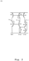
- shows an exemplary embodiment of the signal generator;
- Fig. 3A
- shows a first exemplary embodiment of the Wheatstone bridge circuit;
- Fig. 3B
- shows a second exemplary embodiment of the Wheatstone bridge circuit;
- Fig. 4
- shows an exemplary embodiment of the correlated double sampling block;
- Fig. 5
- shows an exemplary signal progression for the system in the frequency domain;
- Fig. 6
- shows exemplary sub-sampling schemes for the analog-to-digital converter; and
- Fig. 7
- shows an exemplary embodiment of the method according to the second aspect of the invention.
- Reference will now be made in detail to the embodiments of the present invention, examples of which are illustrated in the accompanying drawings. However, the following embodiments of the present invention may be variously modified and the range of the present invention is not limited by the following embodiments. Reference signs for similar entities in different embodiments are partially omitted.
- In
Fig. 1 , an exemplary embodiment of thesystem 100 according to the first aspect of the invention is illustrated. Thesystem 100 may comprise a signal generator (SG) 101 that may generate abiasing signal 102. Thesignal generator 101 may introduce DC offset and/or low-frequency noise components, hereinafter referred as biasing noise components, in thebiasing signal 102. The noise signal introduced by thesignal generator 101 may remain at the baseband or at DC in the frequency spectrum. - The
system 100 may further comprise a first chopper (CHI) 103 operably coupled to thesignal generator 101. Thefirst chopper 103 may receive thebiasing signal 102 from thesignal generator 101 and may modulate thebiasing signal 102 using achopping signal 117 with a chopping frequency fchop to generate a modulatedbiasing signal 104. - The
system 100 may further comprise a Wheatstone bridge circuit (WB) 105 operably coupled to thefirst chopper 103. TheWheatstone bridge circuit 105 may comprise one or more impedance-based sensors. In this regard, theWheatstone bridge circuit 105 may receive the modulatedbiasing signal 104 from thefirst chopper 103 for biasing the circuitry and may accordingly generate asensing signal 106, especially an analog measurement signal, e.g., as a result of the measurements carried out by the one or more impedance-based sensors. - The
system 100 may further comprise a second chopper (CH2) 107 operably coupled to theWheatstone bridge circuit 105. Thesecond chopper 107 may receive thesensing signal 106 from theWheatstone bridge circuit 105, and may modulate thesensing signal 106 using thechopping signal 117 with the chopping frequency fchop to generate a modulatedsensing signal 108. - For the
first chopper 103 and thesecond chopper 107, the term "chopper" should be understood as a multiplier or a modulator that may multiply or mix an input signal with a carrier signal in order to up-modulate or to shift the input signal from the baseband to the frequency of the carrier signal in the frequency spectrum including the generation of corresponding signal harmonics, e.g., due to the modulation with a square wave chopping signal. - The
system 100 may further comprise an amplifier (AMP) 109, especially an instrumentation amplifier (IA), operably coupled to thesecond chopper 107. Theamplifier 109 may receive the modulatedsensing signal 108 from thesecond chopper 107, especially at one or more inputs of theamplifier 109, and may amplify the modulatedsensing signal 108 to generate an amplifiedsignal 110. Theamplifier 109 may be a band-limited amplifier having a bandwidth of about 35×fchop. Alternatively, the amplifier 204 may be designed to have a bandwidth based on the gain accuracy requirements, e.g., a bandwidth lower than 35×fchop that may increase the gain error. - In this regard, the
amplifier 109 may introduce input-referred amplifier DC offset and low-frequency noise components, hereinafter referred as amplifier noise components, while amplifying the modulatedsensing signal 108. The noise signal introduced by theamplifier 109 may remain at the baseband or at DC in the frequency spectrum. - The
system 100 may further comprise a low-pass filter (LPF) 111 operably coupled to theamplifier 109. TheLPF 111 may receive the amplifiedsignal 110 from theamplifier 109, and may filter the amplifiedsignal 110 to generate afiltered signal 112. TheLPF 111 may have a cut-off frequency of about 3.5×fchop. As such, the filteredsignal 112 may comprise one or more harmonic components or chopping harmonics in the frequency spectrum resulted from, e.g., the second chopping operation. - For instance, the
chopping signal 117 may be a square wave of frequency fchop. The first chopping operation at thefirst chopper 103 may up-modulate the biasing noise components at the chopping frequency fchop. Furthermore, the second chopping operation at thesecond chopper 107 may up-modulate thesensing signal 106 at the chopping frequency fchop, while at the same time, may down-modulate the biasing noise components at the baseband or DC in the frequency spectrum. - Hence, the modulated
sensing signal 108 generated by thesecond chopper 107 may comprise thesensing signal 106 at the chopping frequency fchop, a first (odd) harmonic component at thefrequency 3×fchop, a second (odd) harmonic component at the frequency 5×fchop and so on in the frequency spectrum. As theLPF 111 may filter the amplifiedsignal 110 with a cut-off frequency of about 3.5×fchop, the filteredsignal 112 may comprise the biasing noise components and the amplifier noise components at the baseband, thesensing signal 108 at the chopping frequency fchop, and the harmonic component at thefrequency 3×fchop. - The system may further comprise an analog-to-digital converter (ADC) 113 operably coupled to the
LPF 111. TheADC 113 may receive the filteredsignal 112 from theLPF 111, and may perform sub-sampling of the filteredsignal 112 to generatediscrete samples 114. TheADC 113 may sub-sample the filteredsignal 112 with a sampling frequency of N×2×fchop, e.g., with a sampling frequency of 2×fchop for sampling twice during one chopping period Tchop. - The system may further comprise a correlated double sampling (CDS) block 115 operably coupled to the
ADC 114. TheCDS block 115 may operate at the chopping frequency fchop, may receive thesamples 114 from theADC 113, and may perform correlated double sampling operation by subtracting thesamples 114 at the chopping frequency fchop. For example, theADC 113 may provide two samples corresponding to two opposite signal level instances or successive levels. TheCDS block 115 may subtract the samples, which may eliminate or reduce the noise components, however, the useful signal may be doubled in amplitude. - The system may further comprise a chopping signal generator (CSG) 116 operably coupled to the
first chopper 103, thesecond chopper 107, theADC 113, and theCDS block 115. Thechopping signal generator 116 may generate thechopping signal 117 and may provide thechopping signal 117 to thefirst chopper 103 and to thesecond chopper 107. Thesignal generator 116 may further generate thesampling clock 118 for the sub-sampling and may provide thesampling clock 118 to theADC 113. The signal generator may further provide thechopping signal 117 as the CDS clock to theCDS block 115. - It is to be noted that the coupling between the above-mentioned entities, especially between the entities including the
first chopper 103, theWheatstone bridge circuit 105, thesecond chopper 107, theamplifier 109, theLPF 111, and theADC 113, may correspond to a single-ended connection or a differential connection. - In
Fig. 2 , an exemplary embodiment of thesignal generator 101 is illustrated. Thesignal generator 101 may correspond to a biasing current signal generator. The signal generator may comprise a reference current branch (REF) corresponding to the reference current IREF, a PTAT branch corresponding to the IPTAT current as a mirrored or copied version of the IREF, and a CTAT branch corresponding to the ICTAT current as a mirrored or copied version of the IREF. - In this regard, the REF branch may comprise a PFET M4 and an NFET M1, the PTAT branch may comprise a PFET M3 and an NFET M2 that may act as current mirrors, and the CTAT branch may comprise a PFET M5 and an NFET M6 that may also act as current mirrors. Additionally, the PTAT branch may comprise a feedback resistor or conductor or element R that may have a positive temperature coefficient. Furthermore, the CTAT branch may comprise a further NFET M7 that may have a negative temperature coefficient.
- As such, the opposite temperature coefficients may compensate each other, i.e., if the IPTAT and the ICTAT currents may be set to be roughly equal or may be set in a pre-defined ratio, e.g., a ratio of 10 to 1, at some nominal temperature, the resultant current of the IPTAT and the ICTAT currents may become almost temperature independent. Alternatively, the IPTAT and the ICTAT currents may be varied in order to achieve a desired temperature dependency of the resulting biasing current.
- In
Fig. 3A , a first exemplary embodiment of theWheatstone bridge circuit 105 is illustrated. TheWheatstone bridge circuit 105 may comprise a first resistive branch or resistor R1, a second resistive branch or resistor R2, a third resistive branch or resistor R3, and a fourth resistive branch or resistor R4. So the Wheatstone bridge preferably has four resistive branches. It might also have another number of branches, especially an odd number of branches such as six or eight, especially with the same number of branches such as two, three or four, on each side. - Furthermore, the branches or the resistors R1, R2, R3, R4 may be arranged such that a
first node 301 may be formed between R1 and R3, asecond node 302 may be formed between R2 and R4, athird node 303 may be formed between R1 and R2, and afourth node 304 may be formed between R3 and R4. In this regard, at least of the resistors R1, R2, R3, R4 may comprise or be an impedance-based sensor or resistive sensor. In this example, R1 is illustrated as the impedance-based sensor. Alternatively, the resistors R1, R2, R3, R4 each may comprise or be the impedance-based sensor. - For instance, the
nodes Wheatstone bridge circuit 105, i.e., may be coupled to thefirst chopper 103, and thenodes second chopper 107. - Additionally or alternatively, one or more of the resistors R1, R2, R3, R4 may be a variable resistor such that:


- Alternatively, one or more of the resistors R1, R2, R3, R4 may be a variable resistor such that:


- Alternatively, all of the resistors R1, R2, R3, R4 may be a variable resistor such that:


- In
Fig. 3B , a second exemplary embodiment of theWheatstone bridge circuit 105 is illustrated. The second exemplary embodiment ofFig. 3B differs from the first exemplary embodiment ofFig. 3A in that at least one resistive branch or resistor may be replaced with amultiplexer 305. In this example, R1 is replaced with themultiplexer 305. Themultiplexer 305 may be further coupled to one or more impedance-based sensors, exemplarily three impedance-based sensors Rs1, Rs2, Rs3, and may be further coupled to a reference resistor or sensor Rref. - The reference resistor Rref may be used to calibrate the
Wheatstone bridge circuit 105 and/or to generate reference measurements for calibration of theWheatstone bridge circuit 105. Acontrol 306 may be provided to themultiplexer 305 in order to select the sensors Rref, Rs1, Rs2, and Rs3, e.g., to replace R1 ofFig. 3A . - It is to be understood that the
multiplexer 305 can be used to replace any of the resistors R1, R2, R3, R4 in order to select the impedance-based resistor and further to modify the readout path within theWheatstone bridge circuit 105. Additionally or alternatively, more than one resistors R1, R2, R3, R4 can be replaced using the above-described arrangement so that more than one impedance-based sensor can be used. - In
Fig. 4 , an exemplary embodiment of theCDS block 115 is illustrated. TheCDS block 115 may comprise afirst decimation block 401 that may receive theADC samples 114 with a sampling frequency of N×2×fchop and may decimate or down-sample thesamples 114 by N samples, thereby resulting the decimatedsamples 402 at a sampling frequency of 2×fchop. In this regard, thefirst decimation block 401 may perform a zero-order hold operation or sinc filtering to attenuate theADC samples 114. - The
CDS block 115 may further comprise asubtraction block 403 operably coupled to thefirst decimation block 401. Thesubtraction block 403 may operate at the chopping frequency fchop, may receive the decimatedsamples 402 from thefirst decimation block 401, and may subtract thesamples 402 at the chopping frequency fchop to generate subtractedsamples 404. - The
CDS block 115 may further comprise asecond decimation block 405 operably coupled to thesubtraction block 403. Thesecond decimation block 405 may receive the subtractedsamples 404 and may decimate or down-sample thesamples 404 by 2 samples, thereby resulting the further decimatedsamples 406 at a sampling frequency of fchop. In this regard, thesecond decimation block 405 may perform a zero-order hold operation or sinc filtering to attenuate the subtractedsamples 404. - The
CDS block 115 may further comprise athird decimation block 407 operably coupled to thesecond decimation block 405. Thethird decimation block 407 may receive the further decimatedsamples 406 and may decimate or down-sample thesamples 406 to generate the outputdiscrete signal 408 at a suitable frequency, e.g., 40 Hz. In this regard, thethird decimation block 407 may perform a zero-order hold operation or sinc filtering to attenuate the further decimatedsamples 406. TheCDS block 115 may additionally comprise a gain block (not shown), especially coupled to thethird decimation block 407, in order to apply a digital gain at the CDS block output, especially on the outputdiscrete signal 408. - In this regard, the
system 100 may omit theLPF 111, and the digital gain provided by the CDS block 115 may be defined to reduce the gain error to improve the gain accuracy. Alternatively, thesystem 100 may include theLPF 111 and the CDS block 115 may additionally provide the gain in the digital domain at the output of the CDS block 115 to further reduce the gain error, thereby further improving the gain accuracy. - In
Fig. 5 , an exemplary signal progression for thesystem 100, especially in the frequency domain, is illustrated. Thesignal 102 may correspond to thebiasing signal 102 generated by thesignal generator 101. Thesignal 102 comprises the biasingsignal 501, e.g. biasing current, and the biasingnoise components 502 at the baseband. - The
signal 106 may correspond to thefirst chopper output 104 or the Wheatstonebridge circuit output 106. Thesignal 106 comprises thesensing signal 503 at the baseband, however, the biasingnoise components 502 are up-modulated to the chopping frequency fchop due to the first chopping operation at thefirst chopper 103. - The
signal 110 may correspond to thesecond chopper output 108 or theamplifier output 110. Thenoise components biasing noise components 502 are down-modulated to the baseband, however, the amplifier noise components are not affected by any modulation, and therefore remain at the baseband. - Furthermore, the original baseband frequency components of the
sensing signal 503 are modulated and are shown at the odd harmonics, e.g., thefrequency component 503 at fchop, thefrequency component 506 at 3×fchop, thefrequency component 507 at 5×fchop, and so on. - The
signal 112 may correspond to the filter output, i.e., theADC input 112, where theLPF 111 applies a cut-off frequency of 3.5×fchop, as shown by thefilter band 508, especially to include thenoise components frequency component 503 at fchop, and thefrequency component 506 at 3×fchop. - For example, the
second chopper 107 may up-modulate the sensing signal 106 A ∗ cos(ωint), where A is the signal amplitude and ωin is the signal frequency, e.g., with a square wave of +1 and -1. The Fourier expansion of thechopping signal 117 can be expressed as:
- The first term of the modulated
sensing signal 108 can be expressed as:
- It can be understood that the
amplitude 
- The
signal 114 may correspond to theADC output 114, where theADC 113 operates at a sampling frequency of 2×fchop. Particularly, theADC 113 sub-samples all signals greater than fs /2, which results in the amplitude A due to the sub-sampling of thefrequency component 503 at fchop and thefrequency component 506 at 3×fchop, as shown by thefrequency component 509, thereby reducing the gain error. Furthermore, theADC 113 sub-samples the noise components, e.g., the noise components at 2×fchop to the baseband. Moreover, in order to eliminate aliasing, theLPF 111 settles before theADC 113 takes samples. - The
signal 406 may correspond to theCDS block output 406 ofFig. 4 . TheCDS block 115 subtracts the ADC samples at fchop to demodulate thefrequency components 509 back to the baseband, as shown by thefrequency component 510, especially by providing band-pass filtration at fchop. For example, thenoise component 504 at the baseband therefore can be eliminated because of the high-pass filtration at or around fchop or fs /2, and thenoise component 505 can be eliminated or minimized by sample subtraction. The effective exemplary noise components at theCDS block output 408 are shown by the shaded area in the frequency plot, e.g., the noise component at the base band or DC may correspond to the attenuated DC offset of theamplifier 109. - In
Fig. 6 , exemplary sub-sampling schemes for theADC 113 are illustrated. For example, theADC 113 may sub-sample the filteredsignal 112 with a sampling frequency of 2×fchop, i.e., N=1. In this regard, theADC 113 may take samples at the edges of the successive signal levels (top left figure) . Accordingly, the CDS block 115 may subtract said two successive samples, e.g., with a zero-order hold at a sampling frequency of fchop. - As a result of the subtraction and due to the constant level of the noise signal floor, the noise signal can be reduced, while at the same time due to the opposite nature of the actual signal component, the resultant signal may be doubled in amplitude. However, in this example, especially due to the sub-sampling of the noise components because of the band-limited anti-aliasing filtering of the
LPF 111, the signal-to-noise ratio (SNR) may remain the same. - Alternatively, the
ADC 113 may sub-sample the filteredsignal 112 with a sampling frequency of 4×fchop, i.e., N=2. In this regard, theADC 113 may take samples at the edges of the successive signal levels (top right figure). - Further alternatively, the
ADC 113 may sub-sample the filteredsignal 112 with a sampling frequency of 4×fchop, i.e., N=2. In this regard, theADC 113 may take samples at different instances with a defined sampling span on the successive signal levels (bottom left figure). - Further alternatively, the
ADC 113 may sub-sample the filteredsignal 112 with a sampling frequency of 8×fchop, i.e., N=4. In this regard, theADC 113 may take samples at the edges of the successive signal levels (bottom right figure) or may take samples at different instances with a defined sampling span on the successive signal levels (not shown). - In
Fig. 7 , an exemplary embodiment of themethod 700 according to the second aspect of the invention is illustrated. In afirst step 701, a biasing signal is generated. In asecond step 702, the biasing signal is modulated using a chopping signal with a chopping frequency fchop to generate a modulated biasing signal. In athird step 703, the modulated biasing signal is received and a sensing signal is generated based on the modulated biasing signal by a Wheatstone bridge circuit comprising four resistive branches, whereby at least one of the four resistive branches comprises an impedance-based sensor. In afourth step 704, the sensing signal is modulated using the chopping signal with the chopping frequency fchop to generate a modulated sensing signal. - Moreover, in a further step, the modulated sensing signal is amplified to generate an amplified signal. In a further step, the amplified signal is low-pass filtered with a cutoff frequency of at least 3×fchop, preferably a cutoff frequency of 3.5×fchop, to generate a filtered signal. In a further step, the filtered signal is sub-sampled with a sampling frequency of N×2×fchop, where N is an integer. In a further step, a correlated double sampling operation is performed by subtracting the samples at the chopping frequency fchop.
- It is important to note that, in the claims as well as in the description, the word "comprising" does not exclude other elements or steps and the indefinite article "a" or "an" does not exclude a plurality. A single element or other unit may fulfill the functions of several entities or items recited in the claims. Furthermore, the word "coupled" implies that the elements may be directly connected together or may be coupled through one or more intervening elements. Moreover, the description with regard to any of the aspects is also relevant with regard to the other aspects of the invention.
- Although the invention has been illustrated and described with respect to one or more implementations, equivalent alterations and modifications will occur to others skilled in the art upon the reading and understanding of this specification and the annexed drawings. In addition, while a particular feature of the invention may have been disclosed with respect to only one of several implementations, such feature may be combined with one or more other features of the other implementations as may be desired and advantageous for any given or particular application.
Claims (15)
- A sensor readout system (100) comprising:a signal generator (101) configured to generate a biasing signal (102),a first chopper (103) configured to modulate the biasing signal (102) using a chopping signal (117) with a chopping frequency fchop to generate a modulated biasing signal (104),a Wheatstone bridge circuit (105) comprising resistive branches (R1, R2, R3, R4), at least one of the resistive branches comprises an impedance-based sensor (Rs1, Rs2, Rs3), the Wheatstone bridge circuit (105) being configured to receive the modulated biasing signal (104) and to generate a sensing signal (106) based on the modulated biasing signal (104), anda second chopper (107) configured to modulate the sensing signal (106) using the chopping signal (117) with the chopping frequency fchop to generate a modulated sensing signal (108) .
- The sensor readout system according to claim 1,
wherein the sensor readout system further comprises:an amplifier (109) configured to amplify the modulated sensing signal (108) to generate an amplified signal (110),a low-pass filter (111) configured to filter the amplified signal (110) with a cutoff frequency of at least 3×fchop, preferably a cutoff frequency of 3.5×fchop, to generate a filtered signal (112),an analog-to-digital converter (113) configured to sub-sample the filtered signal (112) with a sampling frequency of N×2×fchop, where N is an integer, anda correlated double sampling block (115) configured to perform correlated double sampling operation by subtracting the samples at the chopping frequency fchop. - The sensor readout system according to claim 1 or 2, wherein the sensor readout system further comprises a multiplexer (305) configured to select the impedance-based sensor (Rs1, Rs2, Rs3) from a plurality of impedance-based sensors (Rs1, Rs2, Rs3) and further to couple the impedance-based sensor (Rs1, Rs2, Rs3) to the at least one of preferably the four resistive branches (R1, R2, R3, R4).
- The sensor readout system according to claim 3, wherein the multiplexer (305) is further configured to select a reference resistive element (Rref) having a pre-defined resistance value and further to couple the reference resistive element to the at least one of the preferably four resistive branches (R1, R2, R3, R4).
- The sensor readout system according to any of claims 1 to 4,
wherein at least one of the preferably four resistive branches (R1, R2, R3, R4) comprises a variable resistive element. - The sensor readout system according to any of claims 1 to 5,wherein the signal generator (101) is configured to generate a biasing current as the biasing signal (102), orwherein the signal generator (101) is configured to generate a biasing voltage as the biasing signal (102).
- The sensor readout system according to any of claims 1 to 6,
wherein the signal generator (101) comprises or is a proportional to absolute temperature bias generator. - The sensor readout system according to claim 2, wherein the low-pass filter (111) is configured to settle before the sub-sampling of the filtered signal (112).
- The sensor readout system according to claim 2, wherein the correlated double sampling block (115) is further configured to add a gain factor in digital domain after performing the correlated double sampling operation.
- The sensor readout system according to any of claims 1 to 9,
wherein the impedance-based sensor (Rs1, Rs2, Rs3) is a resistive temperature sensor or a resistive humidity sensor or a resistive pressure sensor or a Piezoresistive sensor. - A sensor readout method (700) comprising:generating (701) a biasing signal (102),modulating (702) the biasing signal (102) using a chopping signal (117) with a chopping frequency fchop to generate a modulated biasing signal (104),receiving (703) the modulated biasing signal (104) and generating a sensing signal (106) based on the modulated biasing signal (104) by a Wheatstone bridge circuit (105) comprising resistive branches (R1, R2, R3, R4), whereby at least one of the resistive branches comprises an impedance-based sensor (Rs1, Rs2, Rs3), andmodulating (704) the sensing signal (106) using the chopping signal (117) with the chopping frequency fchop to generate a modulated sensing signal (108).
- The method according to claim 11,
wherein the method further comprises:amplifying the modulated sensing signal (108) to generate an amplified signal (110),low-pass filtering the amplified signal (110) with a cutoff frequency of at least 3×fchop, preferably a cutoff frequency of 3.5×fchop, to generate a filtered signal (112),sub-sampling the filtered signal (112) with a sampling frequency of N×2×fchop, where N is an integer, andperforming correlated double sampling operation by subtracting the samples at the chopping frequency fchop. - The method according to claim 11 or 12,
wherein the method further comprises:selecting the impedance-based sensor (Rs1, Rs2, Rs3) from a plurality of impedance-based sensors(Rs1, Rs2, Rs3), andcoupling the impedance-based sensor (Rs1, Rs2, Rs3) to the at least one of the preferably four resistive branches (R1, R2, R3, R4). - The method according to any of claims 11 to 13, wherein the method further comprises:selecting a reference resistive element (Rref) having a pre-defined resistance value, andcoupling the reference resistive element to the at least one of the preferably four resistive branches (R1, R2, R3, R4).
- The method according to any of claims 11 to 14, wherein the method further comprises:generating a biasing current as the biasing signal (102), orgenerate a biasing voltage as the biasing signal (102).
Priority Applications (2)
| Application Number | Priority Date | Filing Date | Title |
|---|---|---|---|
| EP22212170.9A EP4382869A1 (en) | 2022-12-08 | 2022-12-08 | Sensor readout system and sensor readout method |
| US18/531,008 US12571657B2 (en) | 2022-12-08 | 2023-12-06 | Sensor readout system and sensor readout method |
Applications Claiming Priority (1)
| Application Number | Priority Date | Filing Date | Title |
|---|---|---|---|
| EP22212170.9A EP4382869A1 (en) | 2022-12-08 | 2022-12-08 | Sensor readout system and sensor readout method |
Publications (1)
| Publication Number | Publication Date |
|---|---|
| EP4382869A1 true EP4382869A1 (en) | 2024-06-12 |
Family
ID=84462610
Family Applications (1)
| Application Number | Title | Priority Date | Filing Date |
|---|---|---|---|
| EP22212170.9A Pending EP4382869A1 (en) | 2022-12-08 | 2022-12-08 | Sensor readout system and sensor readout method |
Country Status (2)
| Country | Link |
|---|---|
| US (1) | US12571657B2 (en) |
| EP (1) | EP4382869A1 (en) |
Citations (3)
| Publication number | Priority date | Publication date | Assignee | Title |
|---|---|---|---|---|
| US5675334A (en) * | 1996-02-12 | 1997-10-07 | Analog Devices, Inc. | Analog to digital conversion system |
| US20170074915A1 (en) * | 2011-04-11 | 2017-03-16 | Melexis Technologies N.V. | Sensor readout with redundancy-checking |
| US20190068146A1 (en) * | 2016-01-15 | 2019-02-28 | Melexis Technologies Sa | Integration-based low noise amplifiers for sensors |
Family Cites Families (7)
| Publication number | Priority date | Publication date | Assignee | Title |
|---|---|---|---|---|
| JP4088247B2 (en) * | 2003-12-25 | 2008-05-21 | 株式会社東芝 | Voltage subtraction circuit and intensity detection circuit using the same |
| GB201119257D0 (en) | 2011-11-08 | 2011-12-21 | Eshtech Ltd | X-ray detection apparatus |
| WO2015026988A1 (en) * | 2013-08-20 | 2015-02-26 | The Regents Of The University Of California | Systems and methods for electrocorticography signal acquisition |
| US9924904B2 (en) * | 2014-09-02 | 2018-03-27 | Medtronic, Inc. | Power-efficient chopper amplifier |
| JP2017147696A (en) * | 2016-02-19 | 2017-08-24 | 株式会社東芝 | Read circuit |
| US11777516B2 (en) * | 2021-02-12 | 2023-10-03 | Cirrus Logic Inc. | Sigma-delta modulator with residue converter for low-offset measurement system |
| EP4060899A1 (en) * | 2021-03-16 | 2022-09-21 | Imec VZW | A sensor readout circuitry, a biopotential signal sensor, a neural probe, and a method for readout of an analog sensor input signal |
-
2022
- 2022-12-08 EP EP22212170.9A patent/EP4382869A1/en active Pending
-
2023
- 2023-12-06 US US18/531,008 patent/US12571657B2/en active Active
Patent Citations (3)
| Publication number | Priority date | Publication date | Assignee | Title |
|---|---|---|---|---|
| US5675334A (en) * | 1996-02-12 | 1997-10-07 | Analog Devices, Inc. | Analog to digital conversion system |
| US20170074915A1 (en) * | 2011-04-11 | 2017-03-16 | Melexis Technologies N.V. | Sensor readout with redundancy-checking |
| US20190068146A1 (en) * | 2016-01-15 | 2019-02-28 | Melexis Technologies Sa | Integration-based low noise amplifiers for sensors |
Also Published As
| Publication number | Publication date |
|---|---|
| US20240192028A1 (en) | 2024-06-13 |
| US12571657B2 (en) | 2026-03-10 |
Similar Documents
| Publication | Publication Date | Title |
|---|---|---|
| US5579247A (en) | Method and apparatus for decreasing the interference and noise sensitivity of a ratiometric converter type of circuit | |
| Nikas et al. | A continuous-time delta-sigma modulator using a modified instrumentation amplifier and current reuse DAC for neural recording | |
| JP5235015B2 (en) | Method for processing a sensor signal subject to an offset and sensor device designed to perform the method | |
| Kashmiri et al. | A temperature-to-digital converter based on an optimized electrothermal filter | |
| US8219331B2 (en) | Electronic device and method for evaluating a variable capacitance | |
| Smith et al. | Design of a phase-sensitive detector to maximize signal-to-noise ratio in the presence of Gaussian wideband noise | |
| CN110971231B (en) | Digital phase-locked amplifier combined with ratio operation | |
| KR20090035574A (en) | Extended Range RMS-DC Converters | |
| US6781361B2 (en) | Apparatus and system for electrical power metering using digital integration | |
| Bianchi et al. | CMOS impedance analyzer for nanosamples investigation operating up to 150 MHz with sub-aF resolution | |
| Gervasoni et al. | Switched ratiometric lock-in amplifier enabling sub-ppm measurements in a wide frequency range | |
| TWI384749B (en) | Chopper amplifier circuit and semiconductor device | |
| Luciani et al. | A miniaturized low-power vector impedance analyser for accurate multi-parameter measurement | |
| FI87960C (en) | FREKVENSSKILLNADSDETEKTOR (FDD) OCH EN BAERVAOGSMODULERAD MOTTAGARE INNEHAOLLANDE EN DYLIK FDD | |
| Yassa et al. | A multichannel digital demodulator for LVDT/RVDT position sensors | |
| US12571657B2 (en) | Sensor readout system and sensor readout method | |
| Gervasoni et al. | FPGA-based lock-in amplifier with sub-ppm resolution working up to 6 MHz | |
| CN113544524A (en) | Magnetic field measuring device and magnetic field measuring method | |
| CN114184856A (en) | Thermal noise detection device based on fully differential structure and noise thermometer | |
| US20060028197A1 (en) | Direct current offset cancellation and phase equalization for power metering devices | |
| US9702898B1 (en) | Method and system for detecting and correcting quadrature error signals for MEMS device | |
| Sarhangnejad et al. | A continuous-time ΣΔ modulator with a Gm-C input stage, 120-dB CMRR and− 87 dB THD | |
| JP2003505966A (en) | Method and apparatus for converting voltage to current | |
| EP4383563A1 (en) | Method and system for processing an analog signal | |
| RU2601262C2 (en) | Method and device for broadband high isolation coupling |
Legal Events
| Date | Code | Title | Description |
|---|---|---|---|
| PUAI | Public reference made under article 153(3) epc to a published international application that has entered the european phase |
Free format text: ORIGINAL CODE: 0009012 |
|
| STAA | Information on the status of an ep patent application or granted ep patent |
Free format text: STATUS: THE APPLICATION HAS BEEN PUBLISHED |
|
| AK | Designated contracting states |
Kind code of ref document: A1 Designated state(s): AL AT BE BG CH CY CZ DE DK EE ES FI FR GB GR HR HU IE IS IT LI LT LU LV MC ME MK MT NL NO PL PT RO RS SE SI SK SM TR |
|
| STAA | Information on the status of an ep patent application or granted ep patent |
Free format text: STATUS: REQUEST FOR EXAMINATION WAS MADE |
|
| 17P | Request for examination filed |
Effective date: 20241202 |
|
| RBV | Designated contracting states (corrected) |
Designated state(s): AL AT BE BG CH CY CZ DE DK EE ES FI FR GB GR HR HU IE IS IT LI LT LU LV MC ME MK MT NL NO PL PT RO RS SE SI SK SM TR |
|
| GRAP | Despatch of communication of intention to grant a patent |
Free format text: ORIGINAL CODE: EPIDOSNIGR1 |
|
| STAA | Information on the status of an ep patent application or granted ep patent |
Free format text: STATUS: GRANT OF PATENT IS INTENDED |
|
| INTG | Intention to grant announced |
Effective date: 20260126 |
|
| GRAS | Grant fee paid |
Free format text: ORIGINAL CODE: EPIDOSNIGR3 |
|
| GRAA | (expected) grant |
Free format text: ORIGINAL CODE: 0009210 |
|
| STAA | Information on the status of an ep patent application or granted ep patent |
Free format text: STATUS: THE PATENT HAS BEEN GRANTED |