EP4380045A1 - Audio amplification circuit, board card, and electronic device - Google Patents
Audio amplification circuit, board card, and electronic device Download PDFInfo
- Publication number
- EP4380045A1 EP4380045A1 EP23833293.6A EP23833293A EP4380045A1 EP 4380045 A1 EP4380045 A1 EP 4380045A1 EP 23833293 A EP23833293 A EP 23833293A EP 4380045 A1 EP4380045 A1 EP 4380045A1
- Authority
- EP
- European Patent Office
- Prior art keywords
- voltage value
- module
- boost
- voltage
- power supply
- Prior art date
- Legal status (The legal status is an assumption and is not a legal conclusion. Google has not performed a legal analysis and makes no representation as to the accuracy of the status listed.)
- Granted
Links
Images




Classifications
-
- H—ELECTRICITY
- H03—ELECTRONIC CIRCUITRY
- H03F—AMPLIFIERS
- H03F1/00—Details of amplifiers with only discharge tubes, only semiconductor devices or only unspecified devices as amplifying elements
- H03F1/30—Modifications of amplifiers to reduce influence of variations of temperature or supply voltage or other physical parameters
-
- H—ELECTRICITY
- H03—ELECTRONIC CIRCUITRY
- H03F—AMPLIFIERS
- H03F3/00—Amplifiers with only discharge tubes or only semiconductor devices as amplifying elements
- H03F3/181—Low-frequency amplifiers, e.g. audio preamplifiers
- H03F3/183—Low-frequency amplifiers, e.g. audio preamplifiers with semiconductor devices only
- H03F3/187—Low-frequency amplifiers, e.g. audio preamplifiers with semiconductor devices only in integrated circuits
-
- H—ELECTRICITY
- H03—ELECTRONIC CIRCUITRY
- H03F—AMPLIFIERS
- H03F3/00—Amplifiers with only discharge tubes or only semiconductor devices as amplifying elements
- H03F3/181—Low-frequency amplifiers, e.g. audio preamplifiers
- H03F3/183—Low-frequency amplifiers, e.g. audio preamplifiers with semiconductor devices only
-
- H—ELECTRICITY
- H03—ELECTRONIC CIRCUITRY
- H03F—AMPLIFIERS
- H03F1/00—Details of amplifiers with only discharge tubes, only semiconductor devices or only unspecified devices as amplifying elements
- H03F1/02—Modifications of amplifiers to raise the efficiency, e.g. gliding Class A stages, use of an auxiliary oscillation
-
- H—ELECTRICITY
- H03—ELECTRONIC CIRCUITRY
- H03F—AMPLIFIERS
- H03F1/00—Details of amplifiers with only discharge tubes, only semiconductor devices or only unspecified devices as amplifying elements
- H03F1/02—Modifications of amplifiers to raise the efficiency, e.g. gliding Class A stages, use of an auxiliary oscillation
- H03F1/0205—Modifications of amplifiers to raise the efficiency, e.g. gliding Class A stages, use of an auxiliary oscillation in transistor amplifiers
- H03F1/0211—Modifications of amplifiers to raise the efficiency, e.g. gliding Class A stages, use of an auxiliary oscillation in transistor amplifiers with control of the supply voltage or current
-
- H—ELECTRICITY
- H03—ELECTRONIC CIRCUITRY
- H03F—AMPLIFIERS
- H03F3/00—Amplifiers with only discharge tubes or only semiconductor devices as amplifying elements
- H03F3/181—Low-frequency amplifiers, e.g. audio preamplifiers
-
- H—ELECTRICITY
- H03—ELECTRONIC CIRCUITRY
- H03F—AMPLIFIERS
- H03F3/00—Amplifiers with only discharge tubes or only semiconductor devices as amplifying elements
- H03F3/20—Power amplifiers, e.g. Class B amplifiers, Class C amplifiers
- H03F3/21—Power amplifiers, e.g. Class B amplifiers, Class C amplifiers with semiconductor devices only
- H03F3/217—Class D power amplifiers; Switching amplifiers
-
- H—ELECTRICITY
- H03—ELECTRONIC CIRCUITRY
- H03G—CONTROL OF AMPLIFICATION
- H03G3/00—Gain control in amplifiers or frequency changers
- H03G3/004—Control by varying the supply voltage
-
- H—ELECTRICITY
- H03—ELECTRONIC CIRCUITRY
- H03G—CONTROL OF AMPLIFICATION
- H03G3/00—Gain control in amplifiers or frequency changers
- H03G3/007—Control dependent on the supply voltage
-
- H—ELECTRICITY
- H04—ELECTRIC COMMUNICATION TECHNIQUE
- H04R—LOUDSPEAKERS, MICROPHONES, GRAMOPHONE PICK-UPS OR LIKE ACOUSTIC ELECTROMECHANICAL TRANSDUCERS; ELECTRIC HEARING AIDS; PUBLIC ADDRESS SYSTEMS
- H04R3/00—Circuits for transducers
-
- H—ELECTRICITY
- H03—ELECTRONIC CIRCUITRY
- H03F—AMPLIFIERS
- H03F2200/00—Indexing scheme relating to amplifiers
- H03F2200/03—Indexing scheme relating to amplifiers the amplifier being designed for audio applications
-
- H—ELECTRICITY
- H03—ELECTRONIC CIRCUITRY
- H03F—AMPLIFIERS
- H03F2200/00—Indexing scheme relating to amplifiers
- H03F2200/513—Indexing scheme relating to amplifiers the amplifier being made for low supply voltages
-
- H—ELECTRICITY
- H04—ELECTRIC COMMUNICATION TECHNIQUE
- H04R—LOUDSPEAKERS, MICROPHONES, GRAMOPHONE PICK-UPS OR LIKE ACOUSTIC ELECTROMECHANICAL TRANSDUCERS; ELECTRIC HEARING AIDS; PUBLIC ADDRESS SYSTEMS
- H04R2499/00—Aspects covered by H04R or H04S not otherwise provided for in their subgroups
- H04R2499/10—General applications
- H04R2499/11—Transducers incorporated or for use in hand-held devices, e.g. mobile phones, PDA's, camera's
-
- Y—GENERAL TAGGING OF NEW TECHNOLOGICAL DEVELOPMENTS; GENERAL TAGGING OF CROSS-SECTIONAL TECHNOLOGIES SPANNING OVER SEVERAL SECTIONS OF THE IPC; TECHNICAL SUBJECTS COVERED BY FORMER USPC CROSS-REFERENCE ART COLLECTIONS [XRACs] AND DIGESTS
- Y02—TECHNOLOGIES OR APPLICATIONS FOR MITIGATION OR ADAPTATION AGAINST CLIMATE CHANGE
- Y02D—CLIMATE CHANGE MITIGATION TECHNOLOGIES IN INFORMATION AND COMMUNICATION TECHNOLOGIES [ICT], I.E. INFORMATION AND COMMUNICATION TECHNOLOGIES AIMING AT THE REDUCTION OF THEIR OWN ENERGY USE
- Y02D30/00—Reducing energy consumption in communication networks
- Y02D30/70—Reducing energy consumption in communication networks in wireless communication networks
Definitions
- This application relates to the field of electronic technologies, and in particular, to an audio amplification circuit, a board, and an electronic device.
- a power supply voltage of an audio amplifier (for example, an audio SmartPA) is usually directly provided by a battery.
- the power supply voltage drops.
- a UVLO under voltage lock out, Under Voltage Lock Out
- the audio amplifier is reset, and consequently, reliability of the audio amplifier is reduced.
- a boost circuit is connected in series with a power supply end.
- the boost circuit connected in series with the power supply end is additionally added, to increase a voltage value of an input voltage of the audio amplifier, for example, as shown in FIG. 2 . In this manner, although the audio amplifier can work at the low voltage, a relatively large power loss may be additionally caused.
- An objective of embodiments of this application is to provide an audio amplification circuit, a board, and an electronic device, to reduce a power loss.
- the specific technical solutions are as follows:
- an audio amplification circuit including:
- the pre-module includes a pre-amplifier and a controller
- the post-module includes a first Boost.
- the boost module is a System Boost
- the System Boost is a native boost module on a board on which the audio amplifier is located.
- the boost module is a second Boost.
- the boost module is a Boost Bypass.
- the audio amplification circuit further includes:
- the voltage determining module includes:
- the voltage measurement submodule is a power management unit or a voltameter
- both the voltage measurement submodule and the system on chip are native devices on a board on which the audio amplifier is located.
- a board including: the audio amplification circuit according to any implementation of the first aspect.
- an electronic device including: the board according to the second aspect.
- Embodiments of this application have the following beneficial effects: Provided in embodiments of this application are an audio amplification circuit, a board, and an electronic device.
- the circuit includes: a boost module and an audio amplifier, where the audio amplifier includes a pre-module and a post-module; an input end of the boost module is connected to a power supply, an output end of the boost module is connected to an input end of the pre-module, and an input end of the post-module is connected to the power supply;
- the boost module is configured to boost a first voltage signal when a voltage value of the received first voltage signal of the power supply is less than a first preset voltage value to obtain a second voltage signal whose voltage value is a second preset voltage value, and send the second voltage signal to the input end of the pre-module, where the second preset voltage value is not less than the first preset voltage value.
- a high-power channel and a low-power channel of the audio amplifier are separated in a dual-rail power supply manner.
- the boost module boosts the first voltage signal of the power supply
- the pre-module the low-power channel
- the post-module the high-power channel
- the audio amplifier can still work stably, and compared with the related art in which the boost module is directly connected in series between the power supply and the audio amplifier, a current flowing through the boost module can be reduced, so that a power loss generated by the boost module is also relatively small. Therefore, by using the audio amplification circuit provided in this application, the power loss is reduced.
- any product or method for implementing this application does not necessarily need to simultaneously achieve all the advantages described above.
- a first end of a power supply is grounded (GND), and a second end of the power supply is respectively connected to a pre-circuit and a post-circuit of the audio amplifier.
- the audio amplifier is directly powered by the power supply.
- the audio amplifier is reset when a voltage signal of the power supply drops below UVLO (under voltage lock out, under voltage lock out) of the audio amplifier, and consequently, the audio amplifier cannot stably work.
- a voltage value of an input voltage of the audio amplifier is increased by directly connecting a boost circuit (Buck Boost or Boost Bypass) in series with the power supply, to ensure stable work of the audio amplifier, as shown in FIG. 2 .
- Boost Boost boost Boost
- FIG. 2 Boost Bypass
- the Buck Boost circuit or the Boost Bypass circuit are simply described below.
- the Buck Boost is a buck-boost circuit and is configured to increase the voltage value of the input voltage of the audio amplifier.
- the Boost Bypass is a boost circuit with a Bypass function.
- the Bypass is a bypass channel.
- the Bypass literally means adding a channel aside for bypassing. In fact, an input is allowed to directly pass through the channel, so that the audio amplifier is directly powered by using a voltage of the power supply greater than the UVLO of the audio amplifier. However, when the voltage of the power supply is lower than the UVLO of the audio amplifier, the Boost (the boost circuit) works to increase the voltage to a state in which the audio amplifier can work.
- embodiments of this application provide an audio amplification circuit, a board, and an electronic device.
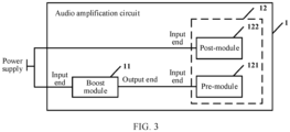
- An audio amplification circuit 1 provided in an embodiment of this application is described in detail below. Referring to FIG. 3 , the circuit includes:
- the power supply may be a battery or a charging and discharging management chip, which is not specifically limited in this application.
- the power supply is the battery, which supplies power to the boost module and the post-module. When battery power is reduced, the voltage value of the first voltage signal is less than the first preset voltage value.
- the first preset voltage value is a voltage value corresponding to UVLO (under voltage lock out) of the audio amplifier.
- the under voltage lock out of the audio amplifier means that when an input voltage of the audio amplifier is less than a value (which refers to the first preset voltage value herein), the pre-module of the audio amplifier cannot meet a working condition, and consequently, the audio amplifier does not work and is in a protection state.
- a specific value of the first preset voltage value is related to a design of the audio amplification circuit and model selection of the audio amplifier and the like, and a specific value of the second preset voltage value is not less than the first preset voltage value, to ensure that a boosted voltage signal enables the pre-module to stably work.
- the first preset voltage value may be set to 3 V
- the pre-module can stably work between 3 V and 5 V
- the second preset voltage value may be set to a voltage value between 3 V and 5 V
- the boost module boosts the first voltage signal to obtain a second voltage signal with a voltage value of 4 V, and sends the second voltage signal to the input end of the pre-module, to ensure that the pre-module meets the working condition, thereby ensuring that the audio amplifier stably works.
- the post-module is a high-power channel of the audio amplifier
- the pre-module is a low-power channel of the audio amplifier.
- Power supplies of the high-power channel and the low-power channel of the audio amplifier are separated (dual-rail power supply).
- the boost module supplies power to the pre-module after boosting the first voltage signal of the power supply, and the post-module is still powered by the power supply.
- the audio amplifier may be classified into class A, class B, class AB, and class D amplifiers.
- the audio amplifier is a SmartPA (which is the class D amplifier for audio amplification).
- the pre-module 121 includes a pre-amplifier 1211 and a controller 1212
- the post-module 122 includes a first Boost 1221.
- the boost module 11 is a System Boost
- the System Boost is a native boost module on a board on which the audio amplifier is located.
- Power supply of a dedicated pin for a battery working mode VBAT; main power supply voltage of direct-through power supply of a charging and discharging management chip: VPH_PWR; boost circuit: Boost; control circuit (controller): Control; and H bridge: H Bridge, configured to convert a direct current signal into an alternating current signal.
- a first end of the power supply is grounded (GND), and A second end of the power supply is respectively connected to an input end of the System Boost and an input end of the first Boost (a first boost circuit) 1221.
- An output end of the System Boost is respectively connected to input ends of the pre-amplifier 1211 and the controller 1212.
- An output end of the pre-amplifier 1211 is connected to a second input end of the H bridge, an output end of the first Boost 1221 is connected to a first input end of the H bridge (H Bridge), and an output end of the H bridge is connected to a speaker.
- the pre-amplifier 1211 is configured to amplify the second voltage signal outputted by the System Boost, and the first Boost 1221 is configured to amplify a voltage signal transmitted by the power supply.
- the speaker is configured to convert the alternating current signal into an acoustic signal.
- the native boost module is described below by using an example.
- the mobile phone board in addition to an audio module, the mobile phone board further includes modules such as a display, a processor, and a radio frequency antenna. These modules also require a Boost, and a System Boost (a system boost circuit) is shared between a plurality of modules, to reduce an area of the board, and reduce costs.
- Boost a system boost circuit
- the boost module 11 is a second Boost.
- the boost module 11 is a Boost Bypass.
- the boost module may be a System Boost, a Boost, or a Boost Bypass.
- the Boost Bypass is a boost with a Bypass function, and the Bypass is a bypass channel.
- a high-power channel and a low-power channel of the audio amplifier are separated in a dual-rail power supply manner.
- the boost module boosts the first voltage signal of the power supply
- the pre-module the low-power channel
- the post-module the high-power channel
- the audio amplifier can still work stably, and compared with the related art in which the boost module is directly connected in series between the power supply and the audio amplifier, a current flowing through the boost module may be reduced, so that a power loss on the boost module is also relatively small. Therefore, the power loss is reduced.
- the audio amplification circuit 1 further includes:
- An input end of the voltage determining module 13 is connected to the power supply, and an output end of the voltage determining module 13 is connected to the controller 1212.
- the voltage determining module is added to detect the voltage value of the first voltage signal of the power supply, and send the reset instruction to the controller when the voltage value of the first voltage signal is less than the third preset voltage value.
- the third preset voltage value is a corresponding voltage value when the voltage of the power supply is low, and a specific value is less than the first preset voltage value.
- a value range of the third preset voltage value may be set to 0 V to 2 V
- the third preset voltage value may be set to 0.5 V
- Sending the reset instruction to the controller means that the voltage determining module detects that the voltage value of the first voltage signal is less than the third preset voltage value.
- the audio amplifier needs to be protected, and the voltage determining module delivers the reset instruction to the controller to actively protect the audio amplifier.
- the controller receives the reset instruction and resets the audio amplifier.
- the voltage determining module when detecting that the voltage value of the first voltage signal of the power supply is less than the third preset voltage value, the voltage determining module sends the reset instruction to the controller, and after receiving the reset instruction, the controller resets the audio amplifier. In this way, the audio amplifier is protected.
- the voltage determining module 13 includes:
- the voltage measurement submodule 131' is a power management unit or a voltameter, and both the voltage measurement submodule 131' and the system on chip 132 are native devices on a board on which the audio amplifier 12 is located.
- the voltage measurement submodule is added to detect the voltage value of the first voltage signal of the power supply, and send the voltage value of the first voltage signal to the system on chip (SOC).
- SOC system on chip
- the system on chip compares the received voltage value of the first voltage signal with the third preset voltage value, and sends the reset instruction to the controller when the received voltage value of the first voltage signal is less than the third preset voltage value.
- the native device is described below by using an example.
- the system on chip (SOC) is not a newly added device.
- a processor in the mobile phone board may be reused, and an effect such as sending a reset instruction to the controller is implemented only by adding a program.
- the voltage measurement submodule is a reused device in the mobile phone board.
- a PMU Power Management Unit, power management unit
- VBAT sampling where the power supply is a battery.
- the SOC starts to poll a battery voltage value sent by the PMU, and sends a polling result to the SmartPA.
- the SmartPA adjusts a system gain corresponding to the battery voltage value by using an automatic gain to ensure that the SmartPA does not cause clipping distortion due to a low voltage.
- the SOC also performs low-voltage alarm judgment.
- the SmartPA is protectively reset. The above operations performed by the SmartPA are performed by a controller of the SmartPA.
- Clipping distortion is described below by using an example.
- a voltage value of the power supply is 2.5 V
- a gain (an amplification factor) of the SmartPA is 6, and a maximum signal of 1/2 V is inputted into the SmartPA.
- the SmartPA should output 6 times (3 V) of this signal to the speaker, but the signal of 3 V is not generated. This is because the power supply is only 2.5 V
- top and bottom ends of the signal may cause distortion, which is clipping distortion.
- the SmartPA adjusts the gain through the controller, and reduces the gain, that is, reduces the amplification factor, so that a volume decreases accordingly to protect the SmartPA from causing clipping distortion.
- the system on chip when the voltage value of the first voltage signal of the power supply is less than the third preset voltage value, the system on chip sends the reset instruction to the controller, thereby achieving protection of the audio amplifier.
- An embodiment of this application further provides a board.
- the board includes any audio amplification circuit described above.
- the board may be a multimedia board or a sound card circuit board, which is not limited in this application.
- An embodiment of this application further provides an electronic device.
- the electronic device includes the board described above.
- the electronic device includes a mobile, a computer, and the like. This is not limited in this application.
- Embodiments of this specification are all described in a relevant manner, for same or similar parts in embodiments, refer to such embodiments, and descriptions of each embodiment focus on a difference from other embodiments.
- a system embodiment is basically similar to a method embodiment, and therefore is described briefly; for related parts, reference may be made to partial descriptions in the method embodiment.
Landscapes
- Engineering & Computer Science (AREA)
- Power Engineering (AREA)
- Multimedia (AREA)
- Physics & Mathematics (AREA)
- Acoustics & Sound (AREA)
- Signal Processing (AREA)
- Microelectronics & Electronic Packaging (AREA)
- Amplifiers (AREA)
Abstract
Description
- This application claims priority to
Chinese Patent Application No. 202211290255.7, entitled "AUDIO AMPLIFICATION CIRCUIT, BOARD, AND ELECTRONIC DEVICE" and filed with the China National Intellectual Property Administration on October 21, 2022 - This application relates to the field of electronic technologies, and in particular, to an audio amplification circuit, a board, and an electronic device.
- In an existing mobile phone system, as shown in
FIG. 1 , a power supply voltage of an audio amplifier (for example, an audio SmartPA) is usually directly provided by a battery. When battery power is reduced, the power supply voltage drops. When the power supply voltage drops below a UVLO (under voltage lock out, Under Voltage Lock Out) voltage of the audio amplifier, the audio amplifier is reset, and consequently, reliability of the audio amplifier is reduced. To ensure that the audio amplifier can still stably work at a low voltage, in the related art, a boost circuit is connected in series with a power supply end. The boost circuit connected in series with the power supply end is additionally added, to increase a voltage value of an input voltage of the audio amplifier, for example, as shown inFIG. 2 . In this manner, although the audio amplifier can work at the low voltage, a relatively large power loss may be additionally caused. - An objective of embodiments of this application is to provide an audio amplification circuit, a board, and an electronic device, to reduce a power loss. The specific technical solutions are as follows:
- According to a first aspect of an embodiment of this application, an audio amplification circuit is provided, including:
- a boost module and an audio amplifier, where the audio amplifier includes a pre-module and a post-module; an input end of the boost module is connected to a power supply, an output end of the boost module is connected to an input end of the pre-module, and an input end of the post-module is connected to the power supply;
- the boost module is configured to boost a first voltage signal when a voltage value of the received first voltage signal of the power supply is less than a first preset voltage value to obtain a second voltage signal whose voltage value is a second preset voltage value, and send the second voltage signal to the input end of the pre-module, where the second preset voltage value is not less than the first preset voltage value.
- In a possible implementation, the pre-module includes a pre-amplifier and a controller, and the post-module includes a first Boost.
- In a possible implementation, the boost module is a System Boost, and the System Boost is a native boost module on a board on which the audio amplifier is located.
- In a possible implementation, the boost module is a second Boost.
- In a possible implementation, the boost module is a Boost Bypass.
- In a possible implementation, the audio amplification circuit further includes:
- a voltage determining module, configured to detect the voltage value of the first voltage signal of the power supply, and send a reset instruction to the controller when the voltage value of the first voltage signal is less than a third preset voltage value, where the third preset voltage value is less than the first preset voltage value; and
- the controller is configured to reset the audio amplifier in response to receiving the reset instruction.
- In a possible implementation, the voltage determining module includes:
- a voltage measurement submodule and a system on chip, where
- the voltage measurement submodule is respectively connected to the power supply and the system on chip, and the system on chip is connected to the controller;
- the voltage measurement submodule is configured to detect the voltage value of the first voltage signal of the power supply, and send the voltage value of the first voltage signal to the system on chip; and
- the system on chip is configured to compare the received voltage value of the first voltage signal with the third preset voltage value, and send the reset instruction to the controller when the received voltage value of the first voltage signal is less than the third preset voltage value.
- In a possible implementation, the voltage measurement submodule is a power management unit or a voltameter, and both the voltage measurement submodule and the system on chip are native devices on a board on which the audio amplifier is located.
- According to a second aspect of an embodiment of this application, a board is provided, including:
the audio amplification circuit according to any implementation of the first aspect. - According to a third aspect of an embodiment of this application, an electronic device is provided, including:
the board according to the second aspect. - Embodiments of this application have the following beneficial effects:
Provided in embodiments of this application are an audio amplification circuit, a board, and an electronic device. The circuit includes: a boost module and an audio amplifier, where the audio amplifier includes a pre-module and a post-module; an input end of the boost module is connected to a power supply, an output end of the boost module is connected to an input end of the pre-module, and an input end of the post-module is connected to the power supply; the boost module is configured to boost a first voltage signal when a voltage value of the received first voltage signal of the power supply is less than a first preset voltage value to obtain a second voltage signal whose voltage value is a second preset voltage value, and send the second voltage signal to the input end of the pre-module, where the second preset voltage value is not less than the first preset voltage value. In the audio amplification circuit provided in this application, a high-power channel and a low-power channel of the audio amplifier are separated in a dual-rail power supply manner. After the boost module boosts the first voltage signal of the power supply, the pre-module (the low-power channel) is powered, and the post-module (the high-power channel) is still powered by the power supply. In this way, it can be ensured that when the voltage value of the power supply drops below the first preset voltage value, the audio amplifier can still work stably, and compared with the related art in which the boost module is directly connected in series between the power supply and the audio amplifier, a current flowing through the boost module can be reduced, so that a power loss generated by the boost module is also relatively small. Therefore, by using the audio amplification circuit provided in this application, the power loss is reduced. - Certainly, any product or method for implementing this application does not necessarily need to simultaneously achieve all the advantages described above.
- The accompanying drawings described herein are used for providing a further understanding of this application, and form part of this application. Exemplary embodiments of this application and descriptions thereof are used for explaining this application, and do not constitute any inappropriate limitation to this application.
-
FIG. 1 is a schematic diagram of a power supply manner of an audio amplifier in the related art; -
FIG. 2 is a schematic diagram of connecting a power supply to a boost circuit in series to supply power in the related art; -
FIG. 3 is a first schematic diagram of an audio amplification circuit according to an embodiment of this application; -
FIG. 4 is a second schematic diagram of an audio amplification circuit according to an embodiment of this application; -
FIG. 5 is a third schematic diagram of an audio amplification circuit according to an embodiment of this application; -
FIG. 6 is a fourth schematic diagram of an audio amplification circuit according to an embodiment of this application; -
FIG. 7 is a fifth schematic diagram of an audio amplification circuit according to an embodiment of this application; and -
FIG. 8 is a schematic flowchart of gain adjustment and reset protection of an audio amplification circuit according to an embodiment of this application. - To make the objectives, technical solutions, and advantages of the present invention clearer and more comprehensible, the following further describes the present invention with reference to the accompanying drawings and embodiments. Apparently, the described embodiments are merely some but not all of embodiments of the present invention. All other embodiments obtained by a person of ordinary skill in the art based on embodiments of the present invention shall fall within the protection scope of the present invention.
- First, a power supply problem existing in a current audio amplifier is simply described.
- As shown in
FIG. 1 , a first end of a power supply is grounded (GND), and a second end of the power supply is respectively connected to a pre-circuit and a post-circuit of the audio amplifier. - The audio amplifier is directly powered by the power supply. The audio amplifier is reset when a voltage signal of the power supply drops below UVLO (under voltage lock out, under voltage lock out) of the audio amplifier, and consequently, the audio amplifier cannot stably work.
- In the related art, a voltage value of an input voltage of the audio amplifier is increased by directly connecting a boost circuit (Buck Boost or Boost Bypass) in series with the power supply, to ensure stable work of the audio amplifier, as shown in
FIG. 2 . However, when such a manner is used, a current flowing through the boost circuit is relatively large, and a power loss generated by the boost circuit is also relatively large. - The Buck Boost circuit or the Boost Bypass circuit are simply described below. The Buck Boost is a buck-boost circuit and is configured to increase the voltage value of the input voltage of the audio amplifier. The Boost Bypass is a boost circuit with a Bypass function. The Bypass is a bypass channel. The Bypass literally means adding a channel aside for bypassing. In fact, an input is allowed to directly pass through the channel, so that the audio amplifier is directly powered by using a voltage of the power supply greater than the UVLO of the audio amplifier. However, when the voltage of the power supply is lower than the UVLO of the audio amplifier, the Boost (the boost circuit) works to increase the voltage to a state in which the audio amplifier can work.
- To reduce the power loss, embodiments of this application provide an audio amplification circuit, a board, and an electronic device.
- An
audio amplification circuit 1 provided in an embodiment of this application is described in detail below. Referring toFIG. 3 , the circuit includes: - a
boost module 11 and anaudio amplifier 12, where theaudio amplifier 12 includes a pre-module 121 and a post-module 122; an input end of theboost module 11 is connected to a power supply, an output end of theboost module 11 is connected to an input end of the pre-module 121, and an input end of the post-module 122 is connected to the power supply; - the
boost module 11 is configured to boost a first voltage signal when a voltage value of the received first voltage signal of the power supply is less than a first preset voltage value to obtain a second voltage signal whose voltage value is a second preset voltage value, and send the second voltage signal to the input end of the pre-module 121, where the second preset voltage value is not less than the first preset voltage value. - The power supply may be a battery or a charging and discharging management chip, which is not specifically limited in this application. In an example, the power supply is the battery, which supplies power to the boost module and the post-module. When battery power is reduced, the voltage value of the first voltage signal is less than the first preset voltage value.
- The first preset voltage value is a voltage value corresponding to UVLO (under voltage lock out) of the audio amplifier. The under voltage lock out of the audio amplifier means that when an input voltage of the audio amplifier is less than a value (which refers to the first preset voltage value herein), the pre-module of the audio amplifier cannot meet a working condition, and consequently, the audio amplifier does not work and is in a protection state. A specific value of the first preset voltage value is related to a design of the audio amplification circuit and model selection of the audio amplifier and the like, and a specific value of the second preset voltage value is not less than the first preset voltage value, to ensure that a boosted voltage signal enables the pre-module to stably work. For example, the first preset voltage value may be set to 3 V, the pre-module can stably work between 3 V and 5 V, and the second preset voltage value may be set to a voltage value between 3 V and 5 V
- In an example, when the voltage value of the first voltage signal of the power supply drops to 2.5 V, the boost module boosts the first voltage signal to obtain a second voltage signal with a voltage value of 4 V, and sends the second voltage signal to the input end of the pre-module, to ensure that the pre-module meets the working condition, thereby ensuring that the audio amplifier stably works.
- The post-module is a high-power channel of the audio amplifier, and the pre-module is a low-power channel of the audio amplifier. Power supplies of the high-power channel and the low-power channel of the audio amplifier are separated (dual-rail power supply). The boost module supplies power to the pre-module after boosting the first voltage signal of the power supply, and the post-module is still powered by the power supply. In this way, it can be ensured that, when a voltage value of the power supply drops below the first preset voltage value, the pre-module of the audio amplifier can stably work, a power loss generated by the boost module is also relatively small, and the post-module is still powered by the power supply, so that power output efficiency is ensured, and the audio amplifier achieves balance between high power output efficiency and a low working voltage.
- The audio amplifier may be classified into class A, class B, class AB, and class D amplifiers. In an example, the audio amplifier is a SmartPA (which is the class D amplifier for audio amplification).
- In a possible implementation, the pre-module 121 includes a
pre-amplifier 1211 and acontroller 1212, and the post-module 122 includes afirst Boost 1221. - In a possible implementation, the
boost module 11 is a System Boost, and the System Boost is a native boost module on a board on which the audio amplifier is located. - As shown in
FIG. 4 , English descriptions corresponding to relevant terms inFIG. 4 are first illustrated, Power supply of a dedicated pin for a battery working mode: VBAT; main power supply voltage of direct-through power supply of a charging and discharging management chip: VPH_PWR; boost circuit: Boost; control circuit (controller): Control; and H bridge: H Bridge, configured to convert a direct current signal into an alternating current signal. - A first end of the power supply is grounded (GND), and A second end of the power supply is respectively connected to an input end of the System Boost and an input end of the first Boost (a first boost circuit) 1221. An output end of the System Boost is respectively connected to input ends of the
pre-amplifier 1211 and thecontroller 1212. An output end of thepre-amplifier 1211 is connected to a second input end of the H bridge, an output end of thefirst Boost 1221 is connected to a first input end of the H bridge (H Bridge), and an output end of the H bridge is connected to a speaker. - The
pre-amplifier 1211 is configured to amplify the second voltage signal outputted by the System Boost, and thefirst Boost 1221 is configured to amplify a voltage signal transmitted by the power supply. - The speaker is configured to convert the alternating current signal into an acoustic signal.
- The native boost module is described below by using an example. By using a mobile phone board as an example, in addition to an audio module, the mobile phone board further includes modules such as a display, a processor, and a radio frequency antenna. These modules also require a Boost, and a System Boost (a system boost circuit) is shared between a plurality of modules, to reduce an area of the board, and reduce costs.
- In a possible implementation, the
boost module 11 is a second Boost. - In a possible implementation, the
boost module 11 is a Boost Bypass. - In an example, the boost module may be a System Boost, a Boost, or a Boost Bypass. The Boost Bypass is a boost with a Bypass function, and the Bypass is a bypass channel.
- In this embodiment of this application, a high-power channel and a low-power channel of the audio amplifier are separated in a dual-rail power supply manner. After the boost module boosts the first voltage signal of the power supply, the pre-module (the low-power channel) is powered, and the post-module (the high-power channel) is still powered by the power supply. In this way, it can be ensured that when the voltage value of the power supply drops below the first preset voltage value, the audio amplifier can still work stably, and compared with the related art in which the boost module is directly connected in series between the power supply and the audio amplifier, a current flowing through the boost module may be reduced, so that a power loss on the boost module is also relatively small. Therefore, the power loss is reduced.
- In a possible implementation, referring to
FIG. 5 , theaudio amplification circuit 1 further includes: - a
voltage determining module 13, configured to detect the voltage value of the first voltage signal of the power supply, and send a reset instruction to thecontroller 1212 when the voltage value of the first voltage signal is less than a third preset voltage value, where the third preset voltage value is less than the first preset voltage value; and - the
controller 1212, configured to reset theaudio amplifier 12 in response to receiving the reset instruction. - An input end of the
voltage determining module 13 is connected to the power supply, and an output end of thevoltage determining module 13 is connected to thecontroller 1212. - In the audio amplification circuit in this application, a power supply pin of the audio amplifier cannot detect a voltage of the power supply. In view of this, the voltage determining module is added to detect the voltage value of the first voltage signal of the power supply, and send the reset instruction to the controller when the voltage value of the first voltage signal is less than the third preset voltage value.
- The third preset voltage value is a corresponding voltage value when the voltage of the power supply is low, and a specific value is less than the first preset voltage value. For example, when the first preset voltage value is 3 V, a value range of the third preset voltage value may be set to 0 V to 2 V In an example, the third preset voltage value may be set to 0.5 V
- Sending the reset instruction to the controller means that the voltage determining module detects that the voltage value of the first voltage signal is less than the third preset voltage value. In this case, the audio amplifier needs to be protected, and the voltage determining module delivers the reset instruction to the controller to actively protect the audio amplifier. The controller receives the reset instruction and resets the audio amplifier.
- In this embodiment of this application, when detecting that the voltage value of the first voltage signal of the power supply is less than the third preset voltage value, the voltage determining module sends the reset instruction to the controller, and after receiving the reset instruction, the controller resets the audio amplifier. In this way, the audio amplifier is protected.
- In a possible implementation, referring to
FIG. 6 , thevoltage determining module 13 includes: - a
voltage measurement submodule 131 and a system onchip 132, where - the
voltage measurement submodule 131 is respectively connected to the power supply and the system onchip 132, and the system onchip 132 is connected to thecontroller 1212; - the
voltage measurement submodule 131 is configured to detect the voltage value of the first voltage signal of the power supply, and send the voltage value of the first voltage signal to the system onchip 132; and - the system on
chip 132 is configured to compare the received voltage value of the first voltage signal with the third preset voltage value, and send the reset instruction to thecontroller 1212 when the received voltage value of the first voltage signal is less than the third preset voltage value. - In a possible implementation, referring to
FIG. 7 , the voltage measurement submodule 131' is a power management unit or a voltameter, and both the voltage measurement submodule 131' and the system onchip 132 are native devices on a board on which theaudio amplifier 12 is located. - In the audio amplification circuit in this application, a power supply pin of the audio amplifier cannot detect a voltage of the power supply. In view of this, the voltage measurement submodule is added to detect the voltage value of the first voltage signal of the power supply, and send the voltage value of the first voltage signal to the system on chip (SOC). The system on chip compares the received voltage value of the first voltage signal with the third preset voltage value, and sends the reset instruction to the controller when the received voltage value of the first voltage signal is less than the third preset voltage value.
- The native device is described below by using an example. By using a mobile phone board as an example, the system on chip (SOC) is not a newly added device. A processor in the mobile phone board may be reused, and an effect such as sending a reset instruction to the controller is implemented only by adding a program. Similarly, the voltage measurement submodule is a reused device in the mobile phone board.
- In an example, as shown in
FIG. 8 , a PMU (Power Management Unit, power management unit) performs VBAT sampling (where the power supply is a battery). After completing volume initialization on the SmartPA (the audio amplifier), the SOC starts to poll a battery voltage value sent by the PMU, and sends a polling result to the SmartPA. After setting an initial gain, the SmartPA adjusts a system gain corresponding to the battery voltage value by using an automatic gain to ensure that the SmartPA does not cause clipping distortion due to a low voltage. The SOC also performs low-voltage alarm judgment. When the battery voltage value is less than the third preset voltage value, the SmartPA is protectively reset. The above operations performed by the SmartPA are performed by a controller of the SmartPA. - Clipping distortion is described below by using an example. A voltage value of the power supply is 2.5 V, a gain (an amplification factor) of the SmartPA is 6, and a maximum signal of 1/2 V is inputted into the SmartPA. The SmartPA should output 6 times (3 V) of this signal to the speaker, but the signal of 3 V is not generated. This is because the power supply is only 2.5 V As a result, top and bottom ends of the signal may cause distortion, which is clipping distortion. In this case, the SmartPA adjusts the gain through the controller, and reduces the gain, that is, reduces the amplification factor, so that a volume decreases accordingly to protect the SmartPA from causing clipping distortion.
- In this embodiment of this application, when the voltage value of the first voltage signal of the power supply is less than the third preset voltage value, the system on chip sends the reset instruction to the controller, thereby achieving protection of the audio amplifier.
- An embodiment of this application further provides a board. The board includes any audio amplification circuit described above.
- The board may be a multimedia board or a sound card circuit board, which is not limited in this application.
- An embodiment of this application further provides an electronic device. The electronic device includes the board described above.
- The electronic device includes a mobile, a computer, and the like. This is not limited in this application.
- It should be noted that the relational terms herein such as first and second are used only to differentiate an entity or operation from another entity or operation, and do not require or imply any actual relationship or sequence between these entities or operations. Moreover, the terms "include," "comprise," and any variation thereof are intended to cover a non-exclusive inclusion. Therefore, in the context of a process, a method, an object, or a device that includes a series of elements, the process, method, object, or device not only includes such elements, but also includes other elements not specified expressly, or may include inherent elements of the process, method, object, or device. Unless otherwise specified, an element limited by "include a/an..." does not exclude other same elements existing in the process, the method, the article, or the device that includes the element.
- Embodiments of this specification are all described in a relevant manner, for same or similar parts in embodiments, refer to such embodiments, and descriptions of each embodiment focus on a difference from other embodiments. Especially, a system embodiment is basically similar to a method embodiment, and therefore is described briefly; for related parts, reference may be made to partial descriptions in the method embodiment.
- The foregoing descriptions are merely preferred embodiments of the present invention and are not intended to limit the present invention. Any modification, equivalent replacement, and improvement made without departing from the spirit and principle of the present invention shall fall within the protection scope of the present invention.
Claims (16)
- An audio amplification circuit, comprising:a boost module and an audio amplifier, wherein the audio amplifier comprises a pre-module and a post-module; an input end of the boost module is connected to a power supply, an output end of the boost module is connected to an input end of the pre-module, and an input end of the post-module is connected to the power supply; andthe boost module is configured to boost a first voltage signal when a voltage value of the received first voltage signal of the power supply is less than a first preset voltage value to obtain a second voltage signal whose voltage value is a second preset voltage value, and send the second voltage signal to the input end of the pre-module, wherein the second preset voltage value is not less than the first preset voltage value.
- The circuit according to claim 1, wherein the pre-module comprises a pre-amplifier and a controller, and the post-module comprises a first Boost.
- The circuit according to claim 1, wherein the boost module is a System Boost, and the System Boost is a native boost module on a board on which the audio amplifier is located.
- The circuit according to claim 1, wherein the boost module is a second Boost.
- The circuit according to claim 1, wherein the boost module is a Boost Bypass.
- The circuit according to claim 2, wherein the audio amplification circuit further comprises:a voltage determining module, configured to detect the voltage value of the first voltage signal of the power supply, and send a reset instruction to the controller when the voltage value of the first voltage signal is less than a third preset voltage value, wherein the third preset voltage value is less than the first preset voltage value; andthe controller, configured to reset the audio amplifier in response to receiving the reset instruction.
- The circuit according to claim 6, wherein the voltage determining module comprises:a voltage measurement submodule and a system on chip, whereinthe voltage measurement submodule is respectively connected to the power supply and the system on chip, and the system on chip is connected to the controller;the voltage measurement submodule is configured to detect the voltage value of the first voltage signal of the power supply, and send the voltage value of the first voltage signal to the system on chip; andthe system on chip is configured to compare the received voltage value of the first voltage signal with the third preset voltage value, and send the reset instruction to the controller when the received voltage value of the first voltage signal is less than the third preset voltage value.
- The circuit according to claim 7, wherein the voltage measurement submodule is a power management unit or a voltameter, and both the voltage measurement submodule and the system on chip are native devices on a board on which the audio amplifier is located.
- An audio amplification circuit, comprising:a boost module, an audio amplifier, and a voltage determining module, whereinthe audio amplifier comprises a pre-module and a post-module, the pre-module comprises a pre-amplifier and a controller, and the post-module comprises a first Boost;an input end of the boost module is connected to a power supply, an output end of the boost module is connected to an input end of the pre-module, and an input end of the post-module is connected to the power supply;the boost module is configured to boost a first voltage signal when a voltage value of the received first voltage signal of the power supply is less than a first preset voltage value to obtain a second voltage signal whose voltage value is a second preset voltage value, and send the second voltage signal to the input end of the pre-module, wherein the second preset voltage value is not less than the first preset voltage value;the voltage determining module is configured to detect the voltage value of the first voltage signal of the power supply, and send a reset instruction to the controller when the voltage value of the first voltage signal is less than a third preset voltage value, wherein the third preset voltage value is less than the first preset voltage value; andthe controller is configured to reset the audio amplifier in response to receiving the reset instruction.
- The circuit according to claim 9, wherein the boost module is a System Boost, and the System Boost is a native boost module on a board on which the audio amplifier is located.
- The circuit according to claim 9, wherein the boost module is a second Boost.
- The circuit according to claim 9, wherein the boost module is a Boost Bypass.
- The circuit according to claim 9, wherein the voltage determining module comprises:a voltage measurement submodule and a system on chip, whereinthe voltage measurement submodule is respectively connected to the power supply and the system on chip, and the system on chip is connected to the controller;the voltage measurement submodule is configured to detect the voltage value of the first voltage signal of the power supply, and send the voltage value of the first voltage signal to the system on chip; andthe system on chip is configured to compare the received voltage value of the first voltage signal with the third preset voltage value, and send the reset instruction to the controller when the received voltage value of the first voltage signal is less than the third preset voltage value.
- The circuit according to claim 13, wherein the voltage measurement submodule is a power management unit or a voltameter, and both the voltage measurement submodule and the system on chip are native devices on a board on which the audio amplifier is located.
- Aboard, comprising:
the audio amplification circuit according to any one of claims 1 to 14. - An electronic device, comprising:
the board according to claim 15.
Applications Claiming Priority (2)
| Application Number | Priority Date | Filing Date | Title |
|---|---|---|---|
| CN202211290255.7A CN115378370B (en) | 2022-10-21 | 2022-10-21 | Audio amplification circuit, board card and electronic equipment |
| PCT/CN2023/117502 WO2024082862A1 (en) | 2022-10-21 | 2023-09-07 | Audio amplification circuit, board card, and electronic device |
Publications (3)
| Publication Number | Publication Date |
|---|---|
| EP4380045A1 true EP4380045A1 (en) | 2024-06-05 |
| EP4380045A4 EP4380045A4 (en) | 2024-11-13 |
| EP4380045B1 EP4380045B1 (en) | 2025-08-27 |
Family
ID=84074005
Family Applications (1)
| Application Number | Title | Priority Date | Filing Date |
|---|---|---|---|
| EP23833293.6A Active EP4380045B1 (en) | 2022-10-21 | 2023-09-07 | Audio amplification circuit, board card, and electronic device |
Country Status (4)
| Country | Link |
|---|---|
| US (1) | US20250105801A1 (en) |
| EP (1) | EP4380045B1 (en) |
| CN (2) | CN115378370B (en) |
| WO (1) | WO2024082862A1 (en) |
Families Citing this family (2)
| Publication number | Priority date | Publication date | Assignee | Title |
|---|---|---|---|---|
| CN115378370B (en) * | 2022-10-21 | 2023-03-31 | 荣耀终端有限公司 | Audio amplification circuit, board card and electronic equipment |
| CN115665632B (en) * | 2022-12-21 | 2023-06-06 | 荣耀终端有限公司 | Audio circuit, related device and control method |
Family Cites Families (17)
| Publication number | Priority date | Publication date | Assignee | Title |
|---|---|---|---|---|
| US6904156B1 (en) * | 2001-08-03 | 2005-06-07 | Zarlink Semiconductor (U.S.) Inc. | System and method for reducing hearing aid squeal |
| EP2648323B1 (en) * | 2012-04-03 | 2018-09-05 | Nxp B.V. | Switched-Mode Power Supply with Feedforward Control based on Load Setpoint |
| US9768689B1 (en) * | 2013-07-26 | 2017-09-19 | Cirrus Logic, Inc. | Controller for imposing current limits on a boost converter for managing thermal loads |
| US9209767B1 (en) * | 2014-05-28 | 2015-12-08 | Motorola Solutions, Inc. | Input current limited power supply and audio power amplifier for high power reproduction of nondeterministic signals |
| EP2999113B1 (en) * | 2014-09-16 | 2019-08-07 | Nxp B.V. | Amplifier |
| EP3332472B1 (en) * | 2015-08-07 | 2020-07-29 | Cirrus Logic International Semiconductor Ltd. | Adjusting peak inductor current to limit supply input current |
| US10021485B2 (en) * | 2015-11-17 | 2018-07-10 | Cirrus Logic, Inc. | Prevention of signal clipping due to decrease in amplifier supply voltage |
| EP3229371B1 (en) * | 2016-04-06 | 2020-03-11 | Nxp B.V. | Audio amplifier system |
| CN206878780U (en) * | 2017-05-09 | 2018-01-12 | 深圳市富满电子集团股份有限公司 | Audio power amplifying circuit |
| US10326405B2 (en) * | 2017-05-18 | 2019-06-18 | Qualcomm Incorporated | Class-H switching amplifier circuit having supply voltage proportional to an audio signal |
| US10917050B2 (en) * | 2018-09-28 | 2021-02-09 | Apple Inc. | Amplifier power converter input current/power limit adjustment using amplifier load determinations |
| US11798501B2 (en) * | 2020-08-25 | 2023-10-24 | Google Llc | Power monitoring for correcting ambient temperature measurement by electronic devices |
| CN112636704B (en) * | 2020-12-07 | 2023-10-20 | Oppo广东移动通信有限公司 | Audio processing circuit and playing device |
| CN113676140B (en) * | 2021-09-26 | 2025-01-03 | 合肥市汤诚集成电路设计有限公司 | An audio power amplifier with adaptive boost control circuit |
| CN216672969U (en) * | 2021-12-15 | 2022-06-03 | 科大讯飞股份有限公司 | Audio power amplifier and automobile sound box |
| US20250386157A1 (en) * | 2022-06-30 | 2025-12-18 | Google Llc | System and method for detecting and correcting audible distortion |
| CN115378370B (en) * | 2022-10-21 | 2023-03-31 | 荣耀终端有限公司 | Audio amplification circuit, board card and electronic equipment |
-
2022
- 2022-10-21 CN CN202211290255.7A patent/CN115378370B/en active Active
- 2022-10-21 CN CN202310256022.3A patent/CN117917854A/en active Pending
-
2023
- 2023-09-07 US US18/291,048 patent/US20250105801A1/en active Pending
- 2023-09-07 EP EP23833293.6A patent/EP4380045B1/en active Active
- 2023-09-07 WO PCT/CN2023/117502 patent/WO2024082862A1/en not_active Ceased
Also Published As
| Publication number | Publication date |
|---|---|
| WO2024082862A1 (en) | 2024-04-25 |
| EP4380045B1 (en) | 2025-08-27 |
| CN117917854A (en) | 2024-04-23 |
| CN115378370A (en) | 2022-11-22 |
| US20250105801A1 (en) | 2025-03-27 |
| CN115378370B (en) | 2023-03-31 |
| EP4380045A4 (en) | 2024-11-13 |
Similar Documents
| Publication | Publication Date | Title |
|---|---|---|
| US20250105801A1 (en) | Audio amplification circuit, board, and electronic device | |
| US11082009B2 (en) | Envelope tracking power amplifier apparatus | |
| US20140315504A1 (en) | Power supply circuit, power supply system, and radio communication apparatus | |
| US20160004267A1 (en) | Dynamic biasing for regulator circuits | |
| US10862432B2 (en) | Power control circuit and power amplifier circuit | |
| US20210227323A1 (en) | Audio signal processing method and apparatus, and device | |
| TWI554121B (en) | Audio processing circuit | |
| US20100201337A1 (en) | Voltage regulator for low noise block | |
| US10073506B2 (en) | Method and system for testing circuit | |
| WO2019154368A1 (en) | Charging apparatus, charging control apparatus, terminal device, and charging method | |
| CN111641243A (en) | Headphone charging circuit and device | |
| CN108388331A (en) | I/O port control circuits and control method, electronic equipment and its control method | |
| US8004366B2 (en) | Area and power efficient, high swing and monolitihic ground centered headphone amplifier circuit operable on a low voltage | |
| CN215576339U (en) | Dynamic booster circuit, electronic device, and audio device | |
| CN113809997A (en) | Power amplifier protection circuit, method, device and electronic device | |
| US20240340582A1 (en) | Coaxial speaker tweeter temperature protection method and system, and computer-readable storage medium | |
| CN211403178U (en) | Auxiliary control circuit of power amplifier module, power amplifier module and communication equipment | |
| US20240388199A1 (en) | Resonant Converter Dynamic Control System and Method Thereof | |
| CN112969128A (en) | Low-distortion audio system | |
| JP6802534B2 (en) | Microphone array | |
| CN112653400A (en) | Amplifying circuit, control method thereof, electronic device, and storage medium | |
| CN112865726A (en) | Power amplification circuit and electronic device | |
| CN216253227U (en) | An audio power supply circuit structure | |
| CN216672969U (en) | Audio power amplifier and automobile sound box | |
| US12563341B2 (en) | Transducer protection system and method |
Legal Events
| Date | Code | Title | Description |
|---|---|---|---|
| STAA | Information on the status of an ep patent application or granted ep patent |
Free format text: STATUS: UNKNOWN |
|
| STAA | Information on the status of an ep patent application or granted ep patent |
Free format text: STATUS: THE INTERNATIONAL PUBLICATION HAS BEEN MADE |
|
| PUAI | Public reference made under article 153(3) epc to a published international application that has entered the european phase |
Free format text: ORIGINAL CODE: 0009012 |
|
| STAA | Information on the status of an ep patent application or granted ep patent |
Free format text: STATUS: REQUEST FOR EXAMINATION WAS MADE |
|
| 17P | Request for examination filed |
Effective date: 20240110 |
|
| AK | Designated contracting states |
Kind code of ref document: A1 Designated state(s): AL AT BE BG CH CY CZ DE DK EE ES FI FR GB GR HR HU IE IS IT LI LT LU LV MC ME MK MT NL NO PL PT RO RS SE SI SK SM TR |
|
| A4 | Supplementary search report drawn up and despatched |
Effective date: 20241014 |
|
| RIC1 | Information provided on ipc code assigned before grant |
Ipc: H04R 3/00 20060101ALI20241008BHEP Ipc: H03F 3/217 20060101ALI20241008BHEP Ipc: H03F 3/187 20060101ALI20241008BHEP Ipc: H03F 1/02 20060101ALI20241008BHEP Ipc: H03G 3/00 20060101ALI20241008BHEP Ipc: H03F 1/30 20060101AFI20241008BHEP |
|
| GRAP | Despatch of communication of intention to grant a patent |
Free format text: ORIGINAL CODE: EPIDOSNIGR1 |
|
| STAA | Information on the status of an ep patent application or granted ep patent |
Free format text: STATUS: GRANT OF PATENT IS INTENDED |
|
| RIC1 | Information provided on ipc code assigned before grant |
Ipc: H04R 3/00 20060101ALI20250306BHEP Ipc: H03F 3/217 20060101ALI20250306BHEP Ipc: H03F 3/187 20060101ALI20250306BHEP Ipc: H03F 1/02 20060101ALI20250306BHEP Ipc: H03G 3/00 20060101ALI20250306BHEP Ipc: H03F 1/30 20060101AFI20250306BHEP |
|
| DAV | Request for validation of the european patent (deleted) | ||
| DAX | Request for extension of the european patent (deleted) | ||
| INTG | Intention to grant announced |
Effective date: 20250320 |
|
| GRAS | Grant fee paid |
Free format text: ORIGINAL CODE: EPIDOSNIGR3 |
|
| GRAA | (expected) grant |
Free format text: ORIGINAL CODE: 0009210 |
|
| STAA | Information on the status of an ep patent application or granted ep patent |
Free format text: STATUS: THE PATENT HAS BEEN GRANTED |
|
| AK | Designated contracting states |
Kind code of ref document: B1 Designated state(s): AL AT BE BG CH CY CZ DE DK EE ES FI FR GB GR HR HU IE IS IT LI LT LU LV MC ME MK MT NL NO PL PT RO RS SE SI SK SM TR |
|
| REG | Reference to a national code |
Ref country code: CH Ref legal event code: EP |
|
| REG | Reference to a national code |
Ref country code: DE Ref legal event code: R096 Ref document number: 602023006178 Country of ref document: DE |
|
| REG | Reference to a national code |
Ref country code: NL Ref legal event code: FP |
|
| REG | Reference to a national code |
Ref country code: IE Ref legal event code: FG4D |
|
| PGFP | Annual fee paid to national office [announced via postgrant information from national office to epo] |
Ref country code: DE Payment date: 20250916 Year of fee payment: 3 |
|
| PGFP | Annual fee paid to national office [announced via postgrant information from national office to epo] |
Ref country code: AT Payment date: 20251020 Year of fee payment: 3 |
|
| PG25 | Lapsed in a contracting state [announced via postgrant information from national office to epo] |
Ref country code: IS Free format text: LAPSE BECAUSE OF FAILURE TO SUBMIT A TRANSLATION OF THE DESCRIPTION OR TO PAY THE FEE WITHIN THE PRESCRIBED TIME-LIMIT Effective date: 20251227 |
|
| PG25 | Lapsed in a contracting state [announced via postgrant information from national office to epo] |
Ref country code: NO Free format text: LAPSE BECAUSE OF FAILURE TO SUBMIT A TRANSLATION OF THE DESCRIPTION OR TO PAY THE FEE WITHIN THE PRESCRIBED TIME-LIMIT Effective date: 20251127 |
|
| REG | Reference to a national code |
Ref country code: LT Ref legal event code: MG9D |
|
| PG25 | Lapsed in a contracting state [announced via postgrant information from national office to epo] |
Ref country code: PT Free format text: LAPSE BECAUSE OF FAILURE TO SUBMIT A TRANSLATION OF THE DESCRIPTION OR TO PAY THE FEE WITHIN THE PRESCRIBED TIME-LIMIT Effective date: 20251229 |
|
| PG25 | Lapsed in a contracting state [announced via postgrant information from national office to epo] |
Ref country code: FI Free format text: LAPSE BECAUSE OF FAILURE TO SUBMIT A TRANSLATION OF THE DESCRIPTION OR TO PAY THE FEE WITHIN THE PRESCRIBED TIME-LIMIT Effective date: 20250827 |
|
| PG25 | Lapsed in a contracting state [announced via postgrant information from national office to epo] |
Ref country code: HR Free format text: LAPSE BECAUSE OF FAILURE TO SUBMIT A TRANSLATION OF THE DESCRIPTION OR TO PAY THE FEE WITHIN THE PRESCRIBED TIME-LIMIT Effective date: 20250827 |
|
| PG25 | Lapsed in a contracting state [announced via postgrant information from national office to epo] |
Ref country code: GR Free format text: LAPSE BECAUSE OF FAILURE TO SUBMIT A TRANSLATION OF THE DESCRIPTION OR TO PAY THE FEE WITHIN THE PRESCRIBED TIME-LIMIT Effective date: 20251128 |
|
| PG25 | Lapsed in a contracting state [announced via postgrant information from national office to epo] |
Ref country code: SE Free format text: LAPSE BECAUSE OF FAILURE TO SUBMIT A TRANSLATION OF THE DESCRIPTION OR TO PAY THE FEE WITHIN THE PRESCRIBED TIME-LIMIT Effective date: 20250827 |
|
| PG25 | Lapsed in a contracting state [announced via postgrant information from national office to epo] |
Ref country code: LV Free format text: LAPSE BECAUSE OF FAILURE TO SUBMIT A TRANSLATION OF THE DESCRIPTION OR TO PAY THE FEE WITHIN THE PRESCRIBED TIME-LIMIT Effective date: 20250827 |
|
| PG25 | Lapsed in a contracting state [announced via postgrant information from national office to epo] |
Ref country code: PL Free format text: LAPSE BECAUSE OF FAILURE TO SUBMIT A TRANSLATION OF THE DESCRIPTION OR TO PAY THE FEE WITHIN THE PRESCRIBED TIME-LIMIT Effective date: 20250827 Ref country code: BG Free format text: LAPSE BECAUSE OF FAILURE TO SUBMIT A TRANSLATION OF THE DESCRIPTION OR TO PAY THE FEE WITHIN THE PRESCRIBED TIME-LIMIT Effective date: 20250827 |
|
| PG25 | Lapsed in a contracting state [announced via postgrant information from national office to epo] |
Ref country code: RS Free format text: LAPSE BECAUSE OF FAILURE TO SUBMIT A TRANSLATION OF THE DESCRIPTION OR TO PAY THE FEE WITHIN THE PRESCRIBED TIME-LIMIT Effective date: 20251127 |
|
| PG25 | Lapsed in a contracting state [announced via postgrant information from national office to epo] |
Ref country code: ES Free format text: LAPSE BECAUSE OF FAILURE TO SUBMIT A TRANSLATION OF THE DESCRIPTION OR TO PAY THE FEE WITHIN THE PRESCRIBED TIME-LIMIT Effective date: 20250827 |
|
| REG | Reference to a national code |
Ref country code: AT Ref legal event code: MK05 Ref document number: 1831217 Country of ref document: AT Kind code of ref document: T Effective date: 20250827 |
|
| PG25 | Lapsed in a contracting state [announced via postgrant information from national office to epo] |
Ref country code: RO Free format text: LAPSE BECAUSE OF FAILURE TO SUBMIT A TRANSLATION OF THE DESCRIPTION OR TO PAY THE FEE WITHIN THE PRESCRIBED TIME-LIMIT Effective date: 20250827 |
|
| PG25 | Lapsed in a contracting state [announced via postgrant information from national office to epo] |
Ref country code: SM Free format text: LAPSE BECAUSE OF FAILURE TO SUBMIT A TRANSLATION OF THE DESCRIPTION OR TO PAY THE FEE WITHIN THE PRESCRIBED TIME-LIMIT Effective date: 20250827 |
|
| PG25 | Lapsed in a contracting state [announced via postgrant information from national office to epo] |
Ref country code: DK Free format text: LAPSE BECAUSE OF FAILURE TO SUBMIT A TRANSLATION OF THE DESCRIPTION OR TO PAY THE FEE WITHIN THE PRESCRIBED TIME-LIMIT Effective date: 20250827 |
|
| PG25 | Lapsed in a contracting state [announced via postgrant information from national office to epo] |
Ref country code: AT Free format text: LAPSE BECAUSE OF FAILURE TO SUBMIT A TRANSLATION OF THE DESCRIPTION OR TO PAY THE FEE WITHIN THE PRESCRIBED TIME-LIMIT Effective date: 20250827 |
|
| PG25 | Lapsed in a contracting state [announced via postgrant information from national office to epo] |
Ref country code: IT Free format text: LAPSE BECAUSE OF FAILURE TO SUBMIT A TRANSLATION OF THE DESCRIPTION OR TO PAY THE FEE WITHIN THE PRESCRIBED TIME-LIMIT Effective date: 20250827 |
|
| PG25 | Lapsed in a contracting state [announced via postgrant information from national office to epo] |
Ref country code: CZ Free format text: LAPSE BECAUSE OF FAILURE TO SUBMIT A TRANSLATION OF THE DESCRIPTION OR TO PAY THE FEE WITHIN THE PRESCRIBED TIME-LIMIT Effective date: 20250827 |
|
| PG25 | Lapsed in a contracting state [announced via postgrant information from national office to epo] |
Ref country code: SK Free format text: LAPSE BECAUSE OF FAILURE TO SUBMIT A TRANSLATION OF THE DESCRIPTION OR TO PAY THE FEE WITHIN THE PRESCRIBED TIME-LIMIT Effective date: 20250827 Ref country code: EE Free format text: LAPSE BECAUSE OF FAILURE TO SUBMIT A TRANSLATION OF THE DESCRIPTION OR TO PAY THE FEE WITHIN THE PRESCRIBED TIME-LIMIT Effective date: 20250827 |