EP4379819A1 - Solar cell and photovoltaic module - Google Patents
Solar cell and photovoltaic module Download PDFInfo
- Publication number
- EP4379819A1 EP4379819A1 EP23159295.7A EP23159295A EP4379819A1 EP 4379819 A1 EP4379819 A1 EP 4379819A1 EP 23159295 A EP23159295 A EP 23159295A EP 4379819 A1 EP4379819 A1 EP 4379819A1
- Authority
- EP
- European Patent Office
- Prior art keywords
- solar cell
- conductive layer
- layer
- doped conductive
- electrode
- Prior art date
- Legal status (The legal status is an assumption and is not a legal conclusion. Google has not performed a legal analysis and makes no representation as to the accuracy of the status listed.)
- Pending
Links
Images


Classifications
-
- H—ELECTRICITY
- H10—SEMICONDUCTOR DEVICES; ELECTRIC SOLID-STATE DEVICES NOT OTHERWISE PROVIDED FOR
- H10F—INORGANIC SEMICONDUCTOR DEVICES SENSITIVE TO INFRARED RADIATION, LIGHT, ELECTROMAGNETIC RADIATION OF SHORTER WAVELENGTH OR CORPUSCULAR RADIATION
- H10F10/00—Individual photovoltaic cells, e.g. solar cells
- H10F10/10—Individual photovoltaic cells, e.g. solar cells having potential barriers
- H10F10/16—Photovoltaic cells having only PN heterojunction potential barriers
- H10F10/164—Photovoltaic cells having only PN heterojunction potential barriers comprising heterojunctions with Group IV materials, e.g. ITO/Si or GaAs/SiGe photovoltaic cells
- H10F10/165—Photovoltaic cells having only PN heterojunction potential barriers comprising heterojunctions with Group IV materials, e.g. ITO/Si or GaAs/SiGe photovoltaic cells the heterojunctions being Group IV-IV heterojunctions, e.g. Si/Ge, SiGe/Si or Si/SiC photovoltaic cells
-
- H—ELECTRICITY
- H10—SEMICONDUCTOR DEVICES; ELECTRIC SOLID-STATE DEVICES NOT OTHERWISE PROVIDED FOR
- H10F—INORGANIC SEMICONDUCTOR DEVICES SENSITIVE TO INFRARED RADIATION, LIGHT, ELECTROMAGNETIC RADIATION OF SHORTER WAVELENGTH OR CORPUSCULAR RADIATION
- H10F10/00—Individual photovoltaic cells, e.g. solar cells
- H10F10/10—Individual photovoltaic cells, e.g. solar cells having potential barriers
- H10F10/17—Photovoltaic cells having only PIN junction potential barriers
- H10F10/174—Photovoltaic cells having only PIN junction potential barriers comprising monocrystalline or polycrystalline materials
-
- H—ELECTRICITY
- H10—SEMICONDUCTOR DEVICES; ELECTRIC SOLID-STATE DEVICES NOT OTHERWISE PROVIDED FOR
- H10F—INORGANIC SEMICONDUCTOR DEVICES SENSITIVE TO INFRARED RADIATION, LIGHT, ELECTROMAGNETIC RADIATION OF SHORTER WAVELENGTH OR CORPUSCULAR RADIATION
- H10F19/00—Integrated devices, or assemblies of multiple devices, comprising at least one photovoltaic cell covered by group H10F10/00, e.g. photovoltaic modules
- H10F19/80—Encapsulations or containers for integrated devices, or assemblies of multiple devices, having photovoltaic cells
-
- H—ELECTRICITY
- H10—SEMICONDUCTOR DEVICES; ELECTRIC SOLID-STATE DEVICES NOT OTHERWISE PROVIDED FOR
- H10F—INORGANIC SEMICONDUCTOR DEVICES SENSITIVE TO INFRARED RADIATION, LIGHT, ELECTROMAGNETIC RADIATION OF SHORTER WAVELENGTH OR CORPUSCULAR RADIATION
- H10F77/00—Constructional details of devices covered by this subclass
- H10F77/30—Coatings
- H10F77/306—Coatings for devices having potential barriers
- H10F77/311—Coatings for devices having potential barriers for photovoltaic cells
-
- H—ELECTRICITY
- H10—SEMICONDUCTOR DEVICES; ELECTRIC SOLID-STATE DEVICES NOT OTHERWISE PROVIDED FOR
- H10F—INORGANIC SEMICONDUCTOR DEVICES SENSITIVE TO INFRARED RADIATION, LIGHT, ELECTROMAGNETIC RADIATION OF SHORTER WAVELENGTH OR CORPUSCULAR RADIATION
- H10F77/00—Constructional details of devices covered by this subclass
- H10F77/30—Coatings
- H10F77/306—Coatings for devices having potential barriers
- H10F77/311—Coatings for devices having potential barriers for photovoltaic cells
- H10F77/315—Coatings for devices having potential barriers for photovoltaic cells the coatings being antireflective or having enhancing optical properties
-
- H—ELECTRICITY
- H10—SEMICONDUCTOR DEVICES; ELECTRIC SOLID-STATE DEVICES NOT OTHERWISE PROVIDED FOR
- H10F—INORGANIC SEMICONDUCTOR DEVICES SENSITIVE TO INFRARED RADIATION, LIGHT, ELECTROMAGNETIC RADIATION OF SHORTER WAVELENGTH OR CORPUSCULAR RADIATION
- H10F19/00—Integrated devices, or assemblies of multiple devices, comprising at least one photovoltaic cell covered by group H10F10/00, e.g. photovoltaic modules
- H10F19/90—Structures for connecting between photovoltaic cells, e.g. interconnections or insulating spacers
- H10F19/902—Structures for connecting between photovoltaic cells, e.g. interconnections or insulating spacers for series or parallel connection of photovoltaic cells
- H10F19/906—Structures for connecting between photovoltaic cells, e.g. interconnections or insulating spacers for series or parallel connection of photovoltaic cells characterised by the materials of the structures
-
- H—ELECTRICITY
- H10—SEMICONDUCTOR DEVICES; ELECTRIC SOLID-STATE DEVICES NOT OTHERWISE PROVIDED FOR
- H10F—INORGANIC SEMICONDUCTOR DEVICES SENSITIVE TO INFRARED RADIATION, LIGHT, ELECTROMAGNETIC RADIATION OF SHORTER WAVELENGTH OR CORPUSCULAR RADIATION
- H10F77/00—Constructional details of devices covered by this subclass
- H10F77/10—Semiconductor bodies
- H10F77/12—Active materials
- H10F77/122—Active materials comprising only Group IV materials
-
- H—ELECTRICITY
- H10—SEMICONDUCTOR DEVICES; ELECTRIC SOLID-STATE DEVICES NOT OTHERWISE PROVIDED FOR
- H10F—INORGANIC SEMICONDUCTOR DEVICES SENSITIVE TO INFRARED RADIATION, LIGHT, ELECTROMAGNETIC RADIATION OF SHORTER WAVELENGTH OR CORPUSCULAR RADIATION
- H10F77/00—Constructional details of devices covered by this subclass
- H10F77/20—Electrodes
- H10F77/206—Electrodes for devices having potential barriers
- H10F77/211—Electrodes for devices having potential barriers for photovoltaic cells
-
- H—ELECTRICITY
- H10—SEMICONDUCTOR DEVICES; ELECTRIC SOLID-STATE DEVICES NOT OTHERWISE PROVIDED FOR
- H10F—INORGANIC SEMICONDUCTOR DEVICES SENSITIVE TO INFRARED RADIATION, LIGHT, ELECTROMAGNETIC RADIATION OF SHORTER WAVELENGTH OR CORPUSCULAR RADIATION
- H10F77/00—Constructional details of devices covered by this subclass
- H10F77/93—Interconnections
- H10F77/933—Interconnections for devices having potential barriers
- H10F77/935—Interconnections for devices having potential barriers for photovoltaic devices or modules
Definitions
- the present disclosure relates to the technical field of solar cells and, in particular, to a solar cell and a photovoltaic module.
- Solar cells can directly convert solar radiation energy into electrical energy.
- a tunneling oxide layer and a doped conductive layer may generally be manufactured on the surface of the substrate to enhance the passivation effect to the substrate.
- an electrode of the solar cell easily penetrates through the tunneling oxide layer to contact the substrate, resulting in destruction of the passivation effect on the surface of the substrate, thus increasing the carrier recombination, and affecting photoelectric conversion efficiency of the solar cells.
- the present disclosure provides a solar cell and a photovoltaic module, which can improve the photoelectric conversion efficiency of the solar cells.
- a solar cell in a first aspect of the present disclosure, includes: a substrate including a first surface; a tunneling oxide layer covering the first surface; a doped conductive layer covering a surface of the tunneling oxide layer away from the substrate; an intrinsic polycrystalline silicon layer formed on one side of the doped conductive layer away from the tunneling oxide layer; and a plurality of first electrodes arranged on one side of the intrinsic polycrystalline silicon layer away from the doped conductive layer and electrically connected to the doped conductive layer. At least a portion of the first electrode is located in the intrinsic polycrystalline silicon layer, and a gap is defined between a top end of the first electrode and the substrate.
- the intrinsic polycrystalline silicon layer covers an entire surface of the doped conductive layer away from the tunneling oxide layer.
- the solar cell further includes a first passivation layer covering a surface of the intrinsic polycrystalline silicon layer away from the doped conductive layer.
- the intrinsic polycrystalline silicon layer includes a plurality of covering portions, and the covering portions cover a surface of the doped conductive layer away from the tunneling oxide layer.
- the covering portions cover parts of the doped conductive layer corresponding to the first electrodes, respectively.
- the solar cell further includes a first passivation layer, one part of the first passivation layer covers a part of the doped conductive layer not provided with the covering portion, and the other part of the first passivation layer covers a surface of the covering portion away from the doped conductive layer.
- a thickness D1 of the intrinsic polycrystalline silicon layer satisfies: 10 nm ⁇ D1 ⁇ 80 nm.
- the solar cell further includes a local doped region connected to the first electrode, the intrinsic polycrystalline silicon layer, and the doped conductive layer, respectively, so that the first electrode is electrically connected to the doped conductive layer.
- the first electrode is a metal electrode
- the first electrode and the doped conductive layer have doping elements of a same conductivity type, and a doping concentration of the first electrode is greater than the doped conductive layer.
- the doping element in the first electrode permeates toward the doped conductive layer to form the local doped region.
- a concentration of the doping element in the doped conductive layer ranges from 1 ⁇ 10 20 atoms/cm 3 to 1 ⁇ 10 21 atoms/cm 3 .
- a concentration of the doping element in the local doped region ranges from 1 ⁇ 10 19 atoms/cm 3 to 1 ⁇ 10 20 atoms/cm 3 .
- the first electrode and the substrate have doping elements of a same conductivity type.
- the first electrode and the substrate have doping elements of different conductivity types.
- a cross-sectional area of the local doped region ranges from 1 ⁇ 10 -8 mm 2 to 1 ⁇ 10 -6 mm 2 .
- the first electrode includes a body portion and an extension portion extending along the body portion toward the doped conductive layer.
- the extension portion is located in the intrinsic polycrystalline silicon layer and/or the doped conductive layer, a gap is defined between a top end of the extension portion and the substrate, and the local doped region covers the extension portion.
- the extension portion includes a first part and a second part, the first part is connected to the body portion, and a gap is defined between the second part and both the body portion and the first part.
- One part of the local doped region covers the first part, and the other part of the local doped region covers the second part.
- a thickness D2 of the doped conductive layer satisfies: 10 nm ⁇ D2 ⁇ 80 nm.
- the substrate further includes a second surface arranged opposite to the first surface.
- the solar cell further includes: an emitter arranged on the second surface; a plurality of second electrodes arranged on one side of the emitter away from the substrate and electrically connected to the emitter; and a second passivation layer covering a surface of the emitter away from the substrate.
- a photovoltaic module in a second aspect of the present disclosure, includes: at least one solar cell string formed by connecting a plurality of solar cells as described in the above aspect; at least one packaging layer configured to cover a surface of the solar cell string; and at least one cover plate configured to cover a surface of the packaging layer away from the solar cell string.
- a tunneling oxide layer and a doped conductive layer may be formed on a surface of a substrate.
- the tunneling oxide layer can be used as a tunneling layer for majority carriers, and chemical passivation is conducted on the surface of the substrate at the same time to reduce interface states.
- the doped conductive layer can form energy band bending, realize selective transport of carriers, reduce loss caused by recombination, and ensure transport efficiency of the carriers.
- a metal electrode may also be manufactured on the surface of the substrate. The metal electrode is electrically connected to the doped conductive layer, and does not penetrate the tunneling oxide layer to maintain good interface passivation effect.
- the doped conductive layer has light absorption capability, which may cause certain optical loss and reduce front cell efficiency and back cell efficiency of the solar cell, thereby reducing double-sided rate of the solar cell, resulting in reduced double-sided power generation rate when the solar cell is configured for double-sided power generation.
- the doped conductive layer may be thinned, thereby reducing the light absorption capability of the doped conductive layer, so as to reduce the optical loss and improve the cell efficiency of the solar cell.
- the metal electrode can easily penetrate the tunneling oxide layer and contact the substrate, resulting in destruction of the passivation effect on the surface of the substrate, thus increasing carrier recombination on the surface of the substrate, and leading to decrease of photoelectric conversion efficiency of the solar cell.
- the solar cell can reduce loss caused by recombination on the surface of the substrate and improve the photoelectric conversion efficiency of the solar cell.
- the solar cell includes a substrate 1, a tunneling oxide layer 2, a doped conductive layer 3, an intrinsic polycrystalline silicon layer 4, and a first electrode 5.
- the substrate 1 has a first surface 1a.
- the tunneling oxide layer 2 covers the first surface 1a.
- the doped conductive layer 3 covers a surface of the tunneling oxide layer away from the substrate 1.
- the intrinsic polycrystalline silicon layer 4 is arranged on one side of the doped conductive layer 3 away from the tunneling oxide layer 2.
- a plurality of first electrodes 5 are arranged on one side of the intrinsic polycrystalline silicon layer 4 away from the doped conductive layer 3, and the plurality of first electrodes 5 are electrically connected to the doped conductive layer 3. At least part of the first electrode 5 is located in the intrinsic polycrystalline silicon layer 4, and a gap exists between a top end of the first electrode 5 and the substrate 1.
- the substrate 1 is configured to receive incident light and generate photo-generated carriers
- the tunneling oxide layer 2 can perform chemical passivation to the first surface 1a and can reduce density of interface defects of the first surface 1a, thereby reducing recombination centers of the first surface 1a to reduce the carrier recombination rate.
- the doped conductive layer 3 is configured to form a field passivation layer, which can reduce concentration of minority carriers, thereby reducing the carrier recombination rate.
- the intrinsic polycrystalline silicon layer 4 is arranged on the side of the doped conductive layer 3 away from the tunneling oxide layer 2, which can increase the distance between the first electrode 5 and the tunneling oxide layer 2.
- At least part of the first electrode 5 can be in contact with the doped conductive layer 3 through the intrinsic polycrystalline silicon layer 4, and be electrically connected to the doped conductive layer 3.
- the existence of the gap between the top end of the first electrode 5 and the substrate 1 ensures that the first electrode 5 will not penetrate the tunneling oxide layer 2 and come into contact with the substrate 1, so that good interface passivation effect can be maintained at the first surface 1a.
- the arrangement of the intrinsic polycrystalline silicon layer 4 can prevent contact of the first electrode 5 with the substrate 1 due to penetration through the tunneling oxide layer 2, thereby preventing damages to the tunneling oxide layer 2, so that good interface passivation effect can be maintained at the first surface 1a, which prevents an increase in carrier recombination and then can improve the photoelectric conversion efficiency of the solar cell, increasing the front cell efficiency, the back cell efficiency, and thus increasing the double-sided rate of the solar cell.
- the intrinsic polycrystalline silicon layer 4 is not doped, and has a light absorption coefficient much lower than the doped conductive layer 3. Therefore, the arrangement of the intrinsic polycrystalline silicon layer 4 can also reduce optical loss of the solar cell and improve utilization of light energy by the solar cell.
- the first electrode 5 not penetrating the tunneling oxide layer 2 includes a situation in which the first electrode 5 is not in contact with the tunneling oxide layer 2 and a situation in which part of the first electrode 5 extends into the tunneling oxide layer 2 but does not completely pass through the tunneling oxide layer 2.
- the substrate 1 may be a silicon substrate, including, but not limited to, a monocrystalline silicon substrate, a polycrystalline silicon substrate, a microcrystalline silicon substrate, a nanocrystalline silicon substrate, and the like.
- the intrinsic polycrystalline silicon layer 4 covers an entire surface of the doped conductive layer 3 away from the tunneling oxide layer 2.
- the intrinsic polycrystalline silicon layer 4 completely covers the surface of the doped conductive layer 3 away from the tunneling oxide layer 2, which can increase the distance between the first electrode 5 and the tunneling oxide layer 2.
- the top end of the first electrode 5 may first contact the intrinsic polycrystalline silicon layer 4 and then contact the doped conductive layer 3, which reduces the possibility that the first electrode 5 penetrates the tunneling oxide layer 2 and contacts the substrate 1.
- the solar cell further includes a first passivation layer 7, and the first passivation layer 7 covers a surface of the intrinsic polycrystalline silicon layer 4 away from the doped conductive layer 3.
- the first passivation layer 7 may play a role of performing passivation on the surface in contact therewith, and is configured to enhance the passivation effect of the solar cell, which can reduce recombination of carriers at the interface and improve transport efficiency of the carriers, thereby improving the photoelectric conversion efficiency of the solar cell.
- the first passivation layer 7 also has the function of reducing or eliminating reflected light on the surface of the solar cell and increasing a light transmission amount, which further improves the photoelectric conversion efficiency of the solar cell.
- the first passivation layer 7 may include components such as silicon oxide, silicon nitride, aluminum oxide, or silicon oxynitride.
- the first passivation layer 7 may have a single-layer structure or a multi-layer structure, and the refractive index and the thickness of each layer may be designed accordingly.
- the intrinsic polycrystalline silicon layer 4 includes a plurality of covering portions 41.
- the covering portions 41 are each configured to cover a surface of the doped conductive layer 3 away from the tunneling oxide layer 2, and the plurality of covering portions 41 cover parts of the doped conductive layer 3 corresponding to the plurality of first electrodes 5, respectively.
- the intrinsic polycrystalline silicon layer 4 is formed by a plurality of covering portions 41 spaced apart from one another.
- Each of the covering portions 41 covers part of a surface of the doped conductive layer 3 and can correspond to one of the plurality of first electrodes 5 to ensure that the first electrode 5 can first contact the covering portion 41 and then contact the doped conductive layer 3, which reduces the possibility that the first electrode 5 penetrates the tunneling oxide layer 2 and contacts the substrate 1.
- the covering portions 41 spaced apart are beneficial to reduce the optical loss of the solar cell, so that more light is absorbed by the substrate 1, and more carriers are generated, thereby improving the photoelectric conversion efficiency of the solar cell. Costs for the arrangement of the intrinsic polycrystalline silicon layer 4 can also be reduced, thereby reducing manufacturing costs of the solar cell.
- the solar cell further includes a first passivation layer 7, one part of the first passivation layer 7 covers a part of the doped conductive layer 3 not provided with the covering portion 41, and the other part of the first passivation layer 7 covers a surface of the covering portion 41 away from the doped conductive layer 3.
- the first passivation layer 7 can completely cover all exposed parts on the surface of the doped conductive layer 3 away from the tunneling oxide layer 2, and can also completely cover surfaces of the covering portions 41 away from the doped conductive layer 3 and side surfaces thereof, which can achieve good passivation effect, thereby reducing recombination of carriers on the surface, improving transport efficiency of the carriers, and then improving the photoelectric conversion efficiency of the solar cell.
- a thickness D1 of the intrinsic polycrystalline silicon layer 4 satisfies: 10 nm ⁇ D1 ⁇ 80 nm.
- the thickness D1 of the intrinsic polycrystalline silicon layer 4 may be 10 nm, 30 nm, 50 nm, 70 nm, or 80 nm, or other values in the above range, which is not limited herein.
- the intrinsic polycrystalline silicon layer 4 is excessively thin. As a result, the distance between the first electrode 5 and the tunneling oxide layer 2 is excessively small, and the first electrode 5 easily penetrates the tunneling oxide layer 2 and contacts the substrate 1, leading to an increase in recombination of the carriers and thus affecting the photoelectric conversion efficiency of the solar cell.
- D1 is excessively large (e.g., greater than 80 nm)
- costs of the intrinsic polycrystalline silicon layer 4 may be increased, but the photoelectric conversion efficiency of the solar cell is not significantly improved. Therefore, when the thickness D1 of the intrinsic polycrystalline silicon layer 4 ranges from 10 nm to 80 nm, the photoelectric conversion efficiency of the solar cell can be improved, and the manufacturing costs of the solar cell can be reduced by a certain amount.
- the solar cell further includes a local doped region 6.
- the local doped region 6 is connected to the first electrode 5, the intrinsic polycrystalline silicon layer 4, and the doped conductive layer 3, respectively, so that the first electrode 5 is electrically connected to the doped conductive layer 3.
- the intrinsic polycrystalline silicon layer 4 includes no doping elements, and the intrinsic polycrystalline silicon layer 4 has weaker conductivity than the doped conductive layer 3.
- the first electrode 5 does not penetrate the intrinsic polycrystalline silicon layer 4, that is, the first electrode 5 is in contact only with the intrinsic polycrystalline silicon layer 4 but not in contact with the doped conductive layer 3, an electrical connection between the first electrode 5 and the doped conductive layer 3 cannot be realized, resulting in reduction in the carrier transport rate. Therefore, there is a need to arrange the local doped region 6 with stronger conductivity to implement the electrical connection between the first electrode 5 and the doped conductive layer 3.
- the local doped region 6 is located in regions of the intrinsic polycrystalline silicon layer 4 and the doped conductive layer 3.
- the local doped region 6 can be connected to the first electrode 5, the intrinsic polycrystalline silicon layer 4, and the doped conductive layer 3 respectively, so as to realize the electrical connection between the first electrode 5 and the doped conductive layer 3 and increase the carrier transport rate.
- the local doped region 6 can improve conduction efficiency between the first electrode 5 and the doped conductive layer 3 on this basis, thereby increasing the carrier transport rate.
- the first electrode 5 is a metal electrode
- the first electrode 5 and the doped conductive layer 3 have doping elements of a same conductivity type, and doping concentration of the first electrode 5 is greater than the doped conductive layer 3.
- the doping element in the first electrode 5 permeates toward the doped conductive layer 3 to form the local doped region 6.
- the doping elements can permeate along concentration gradient from high to low, so as to form, at the intrinsic polycrystalline silicon layer 4 and the doped conductive layer 3, the local doped region 6 extending along the first electrode 5 toward the doped conductive layer 3.
- conductivity of the region can be improved, which is beneficial to realize the electrical connection between the first electrode 5 and the doped conductive layer 3, thereby improving the performance of the solar cell.
- the doping element may be an N-type dopant including Group V elements such as phosphorus (P), arsenic (As), bismuth (Bi), and antimony (Sb), or a P-type dopant including Group III elements such as boron (B), aluminum (Al), gallium (Ga), and indium (In).
- Group V elements such as phosphorus (P), arsenic (As), bismuth (Bi), and antimony (Sb)
- a P-type dopant including Group III elements such as boron (B), aluminum (Al), gallium (Ga), and indium (In).
- the first electrode 5 is sintered from metal electrode paste.
- a doping element in the metal electrode paste accounts for 0.01% to 5% of all components of the paste. For example, it may be 0.01%, 0.05%, 1%, 3%, or 5%, or other values in the above range, which is not limited herein.
- a ratio of doping concentration of the doping element in the local doped region 6 to doping concentration of the doping element in the doped conductive layer 3 ranges from 1:100 to 1:1, and may be 1:100, 1:80, 1:50, 1:30, or 1:1, or other values in the above range, which is not limited herein.
- concentration of the doping element in the doped conductive layer 3 ranges from 1 ⁇ 10 20 atoms/cm 3 to 1 ⁇ 10 21 atoms/cm 3
- concentration of the doping element in the local doped region 6 ranges from 1 ⁇ 10 19 atoms/cm 3 to 1 ⁇ 10 20 atoms/cm 3 .
- the concentration of the doping element in the doped conductive layer 3 may be 1 ⁇ 10 20 atoms/cm 3 , 0.3 ⁇ 10 21 atoms/cm 3 , 0.5 ⁇ 10 21 atoms/cm 3 , 0.8 ⁇ 10 21 atoms/cm 3 , or 1 ⁇ 10 21 atoms/cm 3 , or other values in the above range, which is not limited herein.
- the concentration of the doping element in the local doped region 6 may be 1 ⁇ 10 19 atoms/cm 3 , 0.3 ⁇ 10 20 atoms/cm 3 , 0.5 ⁇ 10 20 atoms/cm 3 , 0.8 ⁇ 10 20 atoms/cm 3 , or 1 ⁇ 10 20 atoms/cm 3 , or other values in the above range, which is not limited herein.
- the first electrode 5 and the substrate 1 have the doping elements of a same conductivity type.
- the doping elements in the first electrode 5 and the substrate 1 are the same, which may be N-type dopants including Group V elements such as P, As, Bi, and Sb, or P-type dopants including Group III elements such as B, Al, Ga, and In.
- the first electrode 5 and the substrate 1 have the doping elements of different conductivity types.
- the doping elements in the first electrode 5 and the substrate 1 are different, when the doping element in the substrate 1 is an N-type dopant including Group V elements such as P, As, Bi, and Sb, the doping element in the first electrode 5 is a P-type dopant including Group III elements such as B, Al, Ga, and In. In some embodiments, when the doping element in the substrate 1 is a P-type dopant including Group III elements such as B, Al, Ga, and In, the doping element in the first electrode 5 is an N-type dopant including Group V elements such as P, As, Bi, and Sb.
- a cross-sectional area of the local doped region 6 ranges from 1 ⁇ 10 -8 mm 2 to 1 ⁇ 10 -6 mm 2 .
- the cross-sectional area of the local doped region 6 may be 1 ⁇ 10 -8 mm 2 , 0.5 ⁇ 10 -7 mm 2 , 1 ⁇ 10 -7 mm 2 , 0.5x 10 -6 mm 2 , or 1 ⁇ 10 -6 mm 2 , or other values in the above range, which is not limited herein.
- the cross-sectional area of the local doped region 6 is excessively small (e.g., less than 1 ⁇ 10 -8 mm 2 ), a contact area between the first electrode 5 and the doped conductive layer 3 may be excessively small, which is not conducive to the transportation of the carriers.
- the cross-sectional area of the local doped region 6 is excessively large (e.g., greater than 1 ⁇ 10 -6 mm 2 )
- the concentration of the doping element in the first electrode 5 is required to be increased, that is, more doping elements are required to be added to the electrode paste, resulting in a substantial increase in manufacturing difficulty and costs of the first electrode 5, but the carrier transport rate may not be significantly increased.
- the contact area between the first electrode 5 and the doped conductive layer 3 can be increased, the carrier transport rate can be increased, and the manufacturing costs of the solar cell can be reduced.
- the first electrode 5 includes a body portion 51 and an extension portion 52 extending along the body portion 51 toward the doped conductive layer 3, the extension portion 52 is located in the intrinsic polycrystalline silicon layer 4 and/or the doped conductive layer 3. A gap exists between a top end of the extension portion 52 and the substrate 1, and the local doped region 6 covers the extension portion 52.
- the body portion 51 is arranged on the side of the intrinsic polycrystalline silicon layer 4 away from the doped conductive layer 3, and the body portion 51 is not in direct contact with the doped conductive layer 3, which can reduce damages to the field passivation layer and ensure that the first surface 1a has good passivation effect.
- the extension portion 52 is electrically connected to the body portion 51, both of which can play a role of transporting the carriers.
- the extension portion 52 extends along the body portion 51 toward the doped conductive layer 3, and the extension portion 52 is formed due to permeation of the electrode paste toward the doped conductive layer 3 during the sintering of the electrode paste.
- the intrinsic polycrystalline silicon layer 4 can prevent penetration of the extension portion 52 through the tunneling oxide layer 2, so that a gap exists between the top end of the extension portion 52 and the substrate 1.
- the local doped region 6 covers a surface of the extension portion 52 not in contact with the body portion 51, and can be connected to the intrinsic polycrystalline silicon layer 4 and the doped conductive layer 3, to realize an electrical connection between the extension portion 52 and the doped conductive layer 3.
- the extension portion 52 includes a first part 521 and a second part 522, the first part 521 is connected to the body portion 51, a gap exists between the second part 522 and both the body portion 51 and the first part 521, one part of the local doped region 6 covers the first part 521, and the other part of the local doped region 6 covers the second part 522.
- the extension portion 52 may be implemented in two forms, one of which is the first part 521 directly connected to the body portion 51 and the other is the second part 522 spaced from the body portion 51.
- the second part 522 is a crystal grain in a free state, and surfaces of the first part 521 and the second part 522 are covered with the local doped region 6 to ensure a stable electrical connection between the extension portion 52 and the doped conductive layer 3.
- a thickness D2 of the doped conductive layer 3 satisfies: 10 nm ⁇ D2 ⁇ 80 nm.
- the thickness D2 of the doped conductive layer 3 may be 10 nm, 30 nm, 50 nm, 70 nm, or 80 nm, or other values in the above range, which is not limited herein.
- the thickness D2 of the doped conductive layer 3 is 10 nm ⁇ D2 ⁇ 80 nm, reliability of the electrical connection between the first electrode 5 and the doped conductive layer 3 can be ensured, the carrier transport rate can be increased, the light absorption capability of the doped conductive layer 3 can be reduced, thereby reducing optical loss of the solar cell and improving cell efficiency of the solar cell, and an overall thickness and weight of the solar cell can also be reduced, thereby facilitating mounting and transportation the solar cell.
- the substrate 1 further has a second surface 1b arranged opposite to the first surface 1a
- the solar cell further includes an emitter 8, a second electrode 9, and a second passivation layer 10.
- the emitter 8 is arranged on the second surface 1b.
- a plurality of second electrodes 9 are arranged on one side of the emitter 8 away from the substrate 1, and the plurality of second electrodes 9 are electrically connected to the emitter 8.
- the second passivation layer 10 covers a surface of the emitter 8 away from the substrate 1.
- Both the first surface 1a and the second surface 1b of the substrate 1 may be configured to receive incident light or reflected light.
- the second surface 1b opposite to the first surface 1a is sequentially provided with the emitter 8, the second electrode 9, and the second passivation layer 10.
- the emitter 8 may be an N-type emitter, and the two may jointly form a PN junction structure.
- the emitter 8 may be a P-type emitter.
- the function and effect of the second passivation layer 10 are close to the first passivation layer 7, which plays a role of performing passivation to the surface in contact therewith, thereby reducing recombination of carriers at the interface, improving transport efficiency of the carriers, and thus improving the photoelectric conversion efficiency of the solar cell.
- the second surface 1b of the substrate 1 may be arranged as a pyramid textured structure, so that reflectivity of the second surface 1b to incident light is reduced, and an absorption utilization rate of light is increased, thereby increasing the light transmission amount of the second surface 1b, and then improving the photoelectric conversion efficiency of the solar cell.
- the first surface 1a of the substrate 1 may be arranged as a non-pyramid textured structure, such as laminated step profile, so that the tunneling oxide layer 2 on the first surface 1a has higher density and uniformity, enabling the tunneling oxide Layer 2 to have good passivation effect on the substrate 1.
- the first surface 1a may be a rear surface of the substrate 1, that is, a surface of the substrate 1 facing away from the sun.
- the second surface 1b may be a front surface of the substrate 1, that is, a surface of the substrate 1 facing the sun and configured to receive sunlight.
- the first surface 1a may also be the front surface of the substrate 1, and correspondingly, the second surface 1b may also be the rear surface of the substrate 1.
- the photovoltaic module includes a solar cell string 110, a packaging layer 120, and a cover plate 130.
- the solar cell string 110 is formed by connecting a plurality of solar cells.
- the solar cells each are the solar cell described in the above embodiments.
- the packaging layer 120 is configured to cover a surface of the solar cell string 110.
- the cover plate 130 is configured to cover a surface of the packaging layer 120 away from the solar cell string 110.
- the solar cells are electrically connected in the form of an entire piece or a plurality of cuts to form a plurality of solar cell strings 110, and the plurality of solar cell strings 110 are electrically connected in series and/or in parallel.
- the plurality of solar cell strings 110 may be electrically connected through conductive strips 140.
- the packaging layer 120 covers a front surface and a rear surface of the solar cell.
- the packaging layer 120 may be an organic packaging adhesive film such as an ethylene vinyl acetate copolymer (EVA) adhesive film, a polyethylene octene co-elastomer (POE) adhesive film, a polyethylene terephthalate (PET) adhesive film, or polyvinyl butyral (PVB).
- EVA ethylene vinyl acetate copolymer
- POE polyethylene octene co-elastomer
- PET polyethylene terephthalate
- PVB polyvinyl butyral
- the cover plate 130 may be a cover plate 130 with a light-transmitting function such as a glass cover plate or a plastic cover plate.
- the surface of the cover plate 130 facing the packaging layer 120 may be a concave-convex surface, thereby increasing the utilization rate of the incident light.
- the solar cell is provided with the intrinsic polycrystalline silicon layer 4, which can prevent the tunneling oxide layer 2 from being damaged by the first electrode 5, improving the photoelectric conversion efficiency of the solar cell, and thus photoelectric conversion efficiency of the photovoltaic module including the solar cell can also be improved.
Landscapes
- Life Sciences & Earth Sciences (AREA)
- Sustainable Development (AREA)
- Engineering & Computer Science (AREA)
- Sustainable Energy (AREA)
- Photovoltaic Devices (AREA)
- Chemical & Material Sciences (AREA)
- Crystallography & Structural Chemistry (AREA)
Abstract
A solar cell and a photovoltaic module. The solar cell includes: a substrate including a first surface; a tunneling oxide layer covering the first surface; a doped conductive layer covering a surface of the tunneling oxide layer away from the substrate; an intrinsic polycrystalline silicon layer formed on one side of the doped conductive layer away from the tunneling oxide layer; and a plurality of first electrodes arranged on one side of the intrinsic polycrystalline silicon layer away from the doped conductive layer and electrically connected to the doped conductive layer. At least a portion of the first electrode is located in the intrinsic polycrystalline silicon layer, and a gap is defined between a top end of the first electrode and the substrate.
Description
- The present disclosure relates to the technical field of solar cells and, in particular, to a solar cell and a photovoltaic module.
- Solar cells can directly convert solar radiation energy into electrical energy. In order to suppress carrier recombination on surface of the substrate of the solar cell, a tunneling oxide layer and a doped conductive layer may generally be manufactured on the surface of the substrate to enhance the passivation effect to the substrate.
- In the related art, an electrode of the solar cell easily penetrates through the tunneling oxide layer to contact the substrate, resulting in destruction of the passivation effect on the surface of the substrate, thus increasing the carrier recombination, and affecting photoelectric conversion efficiency of the solar cells.
- The present disclosure provides a solar cell and a photovoltaic module, which can improve the photoelectric conversion efficiency of the solar cells.
- In a first aspect of the present disclosure, a solar cell is provided, the solar cell includes: a substrate including a first surface; a tunneling oxide layer covering the first surface; a doped conductive layer covering a surface of the tunneling oxide layer away from the substrate; an intrinsic polycrystalline silicon layer formed on one side of the doped conductive layer away from the tunneling oxide layer; and a plurality of first electrodes arranged on one side of the intrinsic polycrystalline silicon layer away from the doped conductive layer and electrically connected to the doped conductive layer. At least a portion of the first electrode is located in the intrinsic polycrystalline silicon layer, and a gap is defined between a top end of the first electrode and the substrate.
- In one or more embodiments, the intrinsic polycrystalline silicon layer covers an entire surface of the doped conductive layer away from the tunneling oxide layer.
- In one or more embodiments, the solar cell further includes a first passivation layer covering a surface of the intrinsic polycrystalline silicon layer away from the doped conductive layer.
- In one or more embodiments, the intrinsic polycrystalline silicon layer includes a plurality of covering portions, and the covering portions cover a surface of the doped conductive layer away from the tunneling oxide layer. The covering portions cover parts of the doped conductive layer corresponding to the first electrodes, respectively.
- In one or more embodiments, the solar cell further includes a first passivation layer, one part of the first passivation layer covers a part of the doped conductive layer not provided with the covering portion, and the other part of the first passivation layer covers a surface of the covering portion away from the doped conductive layer.
- In one or more embodiments, a thickness D1 of the intrinsic polycrystalline silicon layer satisfies: 10 nm≤D1≤80 nm.
- In one or more embodiments, the solar cell further includes a local doped region connected to the first electrode, the intrinsic polycrystalline silicon layer, and the doped conductive layer, respectively, so that the first electrode is electrically connected to the doped conductive layer.
- In one or more embodiments, the first electrode is a metal electrode, the first electrode and the doped conductive layer have doping elements of a same conductivity type, and a doping concentration of the first electrode is greater than the doped conductive layer. The doping element in the first electrode permeates toward the doped conductive layer to form the local doped region.
- In one or more embodiments, a concentration of the doping element in the doped conductive layer ranges from 1×10²⁰ atoms/cm3 to 1×10²¹ atoms/cm3.
- In one or more embodiments, a concentration of the doping element in the local doped region ranges from 1×10¹⁹ atoms/cm3 to 1×10²⁰ atoms/cm3.
- In one or more embodiments, the first electrode and the substrate have doping elements of a same conductivity type.
- In one or more embodiments, the first electrode and the substrate have doping elements of different conductivity types.
- In one or more embodiments, a cross-sectional area of the local doped region ranges from 1×10⁻⁸ mm2 to 1×10⁻⁶ mm2.
- In one or more embodiments, the first electrode includes a body portion and an extension portion extending along the body portion toward the doped conductive layer. The extension portion is located in the intrinsic polycrystalline silicon layer and/or the doped conductive layer, a gap is defined between a top end of the extension portion and the substrate, and the local doped region covers the extension portion.
- In one or more embodiments, the extension portion includes a first part and a second part, the first part is connected to the body portion, and a gap is defined between the second part and both the body portion and the first part. One part of the local doped region covers the first part, and the other part of the local doped region covers the second part.
- In one or more embodiments, a thickness D2 of the doped conductive layer satisfies: 10 nm≤D2≤80 nm.
- In one or more embodiments, the substrate further includes a second surface arranged opposite to the first surface. The solar cell further includes: an emitter arranged on the second surface; a plurality of second electrodes arranged on one side of the emitter away from the substrate and electrically connected to the emitter; and a second passivation layer covering a surface of the emitter away from the substrate.
- In a second aspect of the present disclosure, a photovoltaic module is provided, the photovoltaic module includes: at least one solar cell string formed by connecting a plurality of solar cells as described in the above aspect; at least one packaging layer configured to cover a surface of the solar cell string; and at least one cover plate configured to cover a surface of the packaging layer away from the solar cell string.
- It should be understood that the general description above and the detailed description in the following are merely exemplary and cannot limit the present disclosure.
-
-
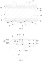
FIG. 1 is a schematic structural diagram of a cross-section of a solar cell according to one or more embodiments of the present disclosure; -
FIG. 2 is a schematic structural diagram of a cross-section of a solar cell according to some other embodiments of the present disclosure; -
FIG. 3 is an enlarged view of Part A inFIG. 1 ; and -
FIG. 4 is a schematic structural diagram of a photovoltaic module according to one or more embodiments of the present disclosure. - The accompanying drawings herein, which are incorporated in and constitute a part of this specification, illustrate embodiments consistent with the present disclosure and, together with the specification, serve to explain principles of the present disclosure.
- In order to better understand the technical solution of the present disclosure, embodiments of the present disclosure are described in detail below with reference to the accompanying drawings.
- It should be made clear that the embodiments described are only some rather than all of the embodiments of the present disclosure. All other embodiments acquired by those of ordinary skill in the art without creative efforts based on the embodiments in the present disclosure fall within the protection scope of the present disclosure.
- The terms used in the embodiments of the present disclosure are intended to describe particular embodiments and are not intended to limit the present disclosure. As used in the specification of the present disclosure and the appended claims, the singular forms of "a/an", "the", and "said" are intended to include plural forms, unless otherwise clearly specified in the context.
- It should be understood that the term "and/or" used herein only describes an association relationship between associated objects and represents that three relationships may exist. For example, A and/or B may represent the following three cases: only A exists, both A and B exist, and only B exists. In addition, the character "/" herein generally means that associated objects are in an "or" relationship.
- It is to be noted that positional terms such as "above", "below", "left", and "right" described in the embodiments of the present disclosure are described from the perspective shown in the drawings and should not be construed as limiting the embodiments of the present disclosure. In addition, in the context, it should be further understood that, when an element is referred to as "above" or "below" another element, it can be directly connected "above" or "below" another element, and can also be indirectly connected "above" or "below" another element through an intermediate element.
- In the related art, when a solar cell is manufactured, a tunneling oxide layer and a doped conductive layer may be formed on a surface of a substrate. The tunneling oxide layer can be used as a tunneling layer for majority carriers, and chemical passivation is conducted on the surface of the substrate at the same time to reduce interface states. The doped conductive layer can form energy band bending, realize selective transport of carriers, reduce loss caused by recombination, and ensure transport efficiency of the carriers. In addition, a metal electrode may also be manufactured on the surface of the substrate. The metal electrode is electrically connected to the doped conductive layer, and does not penetrate the tunneling oxide layer to maintain good interface passivation effect.
- However, the doped conductive layer has light absorption capability, which may cause certain optical loss and reduce front cell efficiency and back cell efficiency of the solar cell, thereby reducing double-sided rate of the solar cell, resulting in reduced double-sided power generation rate when the solar cell is configured for double-sided power generation. In order to improve the above situation, the doped conductive layer may be thinned, thereby reducing the light absorption capability of the doped conductive layer, so as to reduce the optical loss and improve the cell efficiency of the solar cell. However, after the doped conductive layer is thinned, the metal electrode can easily penetrate the tunneling oxide layer and contact the substrate, resulting in destruction of the passivation effect on the surface of the substrate, thus increasing carrier recombination on the surface of the substrate, and leading to decrease of photoelectric conversion efficiency of the solar cell. Moreover, it is difficult to control an existing metal electrode manufacturing process to meet the requirement of "the metal electrode is in contact with the doped conductive layer, but does not penetrate the tunneling oxide layer".
- Based on the above situation, some embodiments of the present disclosure provide a solar cell. The solar cell can reduce loss caused by recombination on the surface of the substrate and improve the photoelectric conversion efficiency of the solar cell. As shown in
FIG. 1 , the solar cell includes asubstrate 1, atunneling oxide layer 2, a dopedconductive layer 3, an intrinsicpolycrystalline silicon layer 4, and afirst electrode 5. Thesubstrate 1 has afirst surface 1a. Thetunneling oxide layer 2 covers thefirst surface 1a. The dopedconductive layer 3 covers a surface of the tunneling oxide layer away from thesubstrate 1. The intrinsicpolycrystalline silicon layer 4 is arranged on one side of the dopedconductive layer 3 away from thetunneling oxide layer 2. A plurality offirst electrodes 5 are arranged on one side of the intrinsicpolycrystalline silicon layer 4 away from the dopedconductive layer 3, and the plurality offirst electrodes 5 are electrically connected to the dopedconductive layer 3. At least part of thefirst electrode 5 is located in the intrinsicpolycrystalline silicon layer 4, and a gap exists between a top end of thefirst electrode 5 and thesubstrate 1. - As shown in
FIG. 1 , thesubstrate 1 is configured to receive incident light and generate photo-generated carriers, thetunneling oxide layer 2 can perform chemical passivation to thefirst surface 1a and can reduce density of interface defects of thefirst surface 1a, thereby reducing recombination centers of thefirst surface 1a to reduce the carrier recombination rate. The dopedconductive layer 3 is configured to form a field passivation layer, which can reduce concentration of minority carriers, thereby reducing the carrier recombination rate. The intrinsicpolycrystalline silicon layer 4 is arranged on the side of the dopedconductive layer 3 away from thetunneling oxide layer 2, which can increase the distance between thefirst electrode 5 and thetunneling oxide layer 2. At least part of thefirst electrode 5 can be in contact with the dopedconductive layer 3 through the intrinsicpolycrystalline silicon layer 4, and be electrically connected to the dopedconductive layer 3. The existence of the gap between the top end of thefirst electrode 5 and thesubstrate 1 ensures that thefirst electrode 5 will not penetrate thetunneling oxide layer 2 and come into contact with thesubstrate 1, so that good interface passivation effect can be maintained at thefirst surface 1a. - In one or more embodiments, the arrangement of the intrinsic
polycrystalline silicon layer 4 can prevent contact of thefirst electrode 5 with thesubstrate 1 due to penetration through thetunneling oxide layer 2, thereby preventing damages to thetunneling oxide layer 2, so that good interface passivation effect can be maintained at thefirst surface 1a, which prevents an increase in carrier recombination and then can improve the photoelectric conversion efficiency of the solar cell, increasing the front cell efficiency, the back cell efficiency, and thus increasing the double-sided rate of the solar cell. Moreover, the intrinsicpolycrystalline silicon layer 4 is not doped, and has a light absorption coefficient much lower than the dopedconductive layer 3. Therefore, the arrangement of the intrinsicpolycrystalline silicon layer 4 can also reduce optical loss of the solar cell and improve utilization of light energy by the solar cell. - It is to be noted that the
first electrode 5 not penetrating thetunneling oxide layer 2 includes a situation in which thefirst electrode 5 is not in contact with thetunneling oxide layer 2 and a situation in which part of thefirst electrode 5 extends into thetunneling oxide layer 2 but does not completely pass through thetunneling oxide layer 2. - In one or more embodiments, the
substrate 1 may be a silicon substrate, including, but not limited to, a monocrystalline silicon substrate, a polycrystalline silicon substrate, a microcrystalline silicon substrate, a nanocrystalline silicon substrate, and the like. - In some embodiments, as shown in
FIG. 1 , the intrinsicpolycrystalline silicon layer 4 covers an entire surface of the dopedconductive layer 3 away from thetunneling oxide layer 2. - The intrinsic
polycrystalline silicon layer 4 completely covers the surface of the dopedconductive layer 3 away from thetunneling oxide layer 2, which can increase the distance between thefirst electrode 5 and thetunneling oxide layer 2. In the process of sintering electrode paste to form thefirst electrode 5, the top end of thefirst electrode 5 may first contact the intrinsicpolycrystalline silicon layer 4 and then contact the dopedconductive layer 3, which reduces the possibility that thefirst electrode 5 penetrates thetunneling oxide layer 2 and contacts thesubstrate 1. - In some embodiments, as shown in
FIG. 1 , the solar cell further includes afirst passivation layer 7, and thefirst passivation layer 7 covers a surface of the intrinsicpolycrystalline silicon layer 4 away from the dopedconductive layer 3. - The
first passivation layer 7 may play a role of performing passivation on the surface in contact therewith, and is configured to enhance the passivation effect of the solar cell, which can reduce recombination of carriers at the interface and improve transport efficiency of the carriers, thereby improving the photoelectric conversion efficiency of the solar cell. Thefirst passivation layer 7 also has the function of reducing or eliminating reflected light on the surface of the solar cell and increasing a light transmission amount, which further improves the photoelectric conversion efficiency of the solar cell. - In some embodiments, the
first passivation layer 7 may include components such as silicon oxide, silicon nitride, aluminum oxide, or silicon oxynitride. In addition, thefirst passivation layer 7 may have a single-layer structure or a multi-layer structure, and the refractive index and the thickness of each layer may be designed accordingly. - In addition, in some other embodiments, as shown in
FIG. 2 , the intrinsicpolycrystalline silicon layer 4 includes a plurality of coveringportions 41. The coveringportions 41 are each configured to cover a surface of the dopedconductive layer 3 away from thetunneling oxide layer 2, and the plurality of coveringportions 41 cover parts of the dopedconductive layer 3 corresponding to the plurality offirst electrodes 5, respectively. - In one or more embodiments, the intrinsic
polycrystalline silicon layer 4 is formed by a plurality of coveringportions 41 spaced apart from one another. Each of the coveringportions 41 covers part of a surface of the dopedconductive layer 3 and can correspond to one of the plurality offirst electrodes 5 to ensure that thefirst electrode 5 can first contact the coveringportion 41 and then contact the dopedconductive layer 3, which reduces the possibility that thefirst electrode 5 penetrates thetunneling oxide layer 2 and contacts thesubstrate 1. On this basis, the coveringportions 41 spaced apart are beneficial to reduce the optical loss of the solar cell, so that more light is absorbed by thesubstrate 1, and more carriers are generated, thereby improving the photoelectric conversion efficiency of the solar cell. Costs for the arrangement of the intrinsicpolycrystalline silicon layer 4 can also be reduced, thereby reducing manufacturing costs of the solar cell. - In some embodiments, as shown in
FIG. 2 , the solar cell further includes afirst passivation layer 7, one part of thefirst passivation layer 7 covers a part of the dopedconductive layer 3 not provided with the coveringportion 41, and the other part of thefirst passivation layer 7 covers a surface of the coveringportion 41 away from the dopedconductive layer 3. - As shown in
FIG. 2 , thefirst passivation layer 7 can completely cover all exposed parts on the surface of the dopedconductive layer 3 away from thetunneling oxide layer 2, and can also completely cover surfaces of the coveringportions 41 away from the dopedconductive layer 3 and side surfaces thereof, which can achieve good passivation effect, thereby reducing recombination of carriers on the surface, improving transport efficiency of the carriers, and then improving the photoelectric conversion efficiency of the solar cell. - In some embodiments, as shown in
FIG. 3 , a thickness D1 of the intrinsicpolycrystalline silicon layer 4 satisfies: 10 nm≤D1≤80 nm. For example, the thickness D1 of the intrinsicpolycrystalline silicon layer 4 may be 10 nm, 30 nm, 50 nm, 70 nm, or 80 nm, or other values in the above range, which is not limited herein. - When D1 is excessively small (e.g., less than 10 nm), the intrinsic
polycrystalline silicon layer 4 is excessively thin. As a result, the distance between thefirst electrode 5 and thetunneling oxide layer 2 is excessively small, and thefirst electrode 5 easily penetrates thetunneling oxide layer 2 and contacts thesubstrate 1, leading to an increase in recombination of the carriers and thus affecting the photoelectric conversion efficiency of the solar cell. When D1 is excessively large (e.g., greater than 80 nm), costs of the intrinsicpolycrystalline silicon layer 4 may be increased, but the photoelectric conversion efficiency of the solar cell is not significantly improved. Therefore, when the thickness D1 of the intrinsicpolycrystalline silicon layer 4 ranges from 10 nm to 80 nm, the photoelectric conversion efficiency of the solar cell can be improved, and the manufacturing costs of the solar cell can be reduced by a certain amount. - In some embodiments, as shown in
FIG. 3 , the solar cell further includes a localdoped region 6. The localdoped region 6 is connected to thefirst electrode 5, the intrinsicpolycrystalline silicon layer 4, and the dopedconductive layer 3, respectively, so that thefirst electrode 5 is electrically connected to the dopedconductive layer 3. - The intrinsic
polycrystalline silicon layer 4 includes no doping elements, and the intrinsicpolycrystalline silicon layer 4 has weaker conductivity than the dopedconductive layer 3. When thefirst electrode 5 does not penetrate the intrinsicpolycrystalline silicon layer 4, that is, thefirst electrode 5 is in contact only with the intrinsicpolycrystalline silicon layer 4 but not in contact with the dopedconductive layer 3, an electrical connection between thefirst electrode 5 and the dopedconductive layer 3 cannot be realized, resulting in reduction in the carrier transport rate. Therefore, there is a need to arrange the localdoped region 6 with stronger conductivity to implement the electrical connection between thefirst electrode 5 and the dopedconductive layer 3. - In some embodiments, as shown in
FIG. 3 , the localdoped region 6 is located in regions of the intrinsicpolycrystalline silicon layer 4 and the dopedconductive layer 3. When thefirst electrode 5 does not penetrate the intrinsicpolycrystalline silicon layer 4, the localdoped region 6 can be connected to thefirst electrode 5, the intrinsicpolycrystalline silicon layer 4, and the dopedconductive layer 3 respectively, so as to realize the electrical connection between thefirst electrode 5 and the dopedconductive layer 3 and increase the carrier transport rate. When thefirst electrode 5 penetrates the intrinsicpolycrystalline silicon layer 4 and contacts the dopedconductive layer 3 to form the electrical connection, the localdoped region 6 can improve conduction efficiency between thefirst electrode 5 and the dopedconductive layer 3 on this basis, thereby increasing the carrier transport rate. - In some embodiments, the
first electrode 5 is a metal electrode, thefirst electrode 5 and the dopedconductive layer 3 have doping elements of a same conductivity type, and doping concentration of thefirst electrode 5 is greater than the dopedconductive layer 3. The doping element in thefirst electrode 5 permeates toward the dopedconductive layer 3 to form the localdoped region 6. - When the
first electrode 5 and the dopedconductive layer 3 have the doping elements of the same conductivity type and the doping concentration of thefirst electrode 5 is greater than the dopedconductive layer 3, in a high-temperature process of sintering the electrode paste, the doping elements can permeate along concentration gradient from high to low, so as to form, at the intrinsicpolycrystalline silicon layer 4 and the dopedconductive layer 3, the localdoped region 6 extending along thefirst electrode 5 toward the dopedconductive layer 3. After the localdoped region 6 is formed in part of the region of the intrinsicpolycrystalline silicon layer 4, conductivity of the region can be improved, which is beneficial to realize the electrical connection between thefirst electrode 5 and the dopedconductive layer 3, thereby improving the performance of the solar cell. - In some embodiments, the doping element may be an N-type dopant including Group V elements such as phosphorus (P), arsenic (As), bismuth (Bi), and antimony (Sb), or a P-type dopant including Group III elements such as boron (B), aluminum (Al), gallium (Ga), and indium (In).
- In addition, the
first electrode 5 is sintered from metal electrode paste. A doping element in the metal electrode paste accounts for 0.01% to 5% of all components of the paste. For example, it may be 0.01%, 0.05%, 1%, 3%, or 5%, or other values in the above range, which is not limited herein. - After the local
doped region 6 is formed, a ratio of doping concentration of the doping element in the localdoped region 6 to doping concentration of the doping element in the dopedconductive layer 3 ranges from 1:100 to 1:1, and may be 1:100, 1:80, 1:50, 1:30, or 1:1, or other values in the above range, which is not limited herein. - In some embodiments, concentration of the doping element in the doped
conductive layer 3 ranges from 1×10²⁰ atoms/cm3 to 1×10²¹ atoms/cm3, and concentration of the doping element in the localdoped region 6 ranges from 1×10¹⁹ atoms/cm3 to 1×10²⁰ atoms/cm3. - In some embodiments, the concentration of the doping element in the doped
conductive layer 3 may be 1×10²⁰ atoms/cm3, 0.3×10²¹ atoms/cm3, 0.5×10²¹ atoms/cm3, 0.8×10²¹ atoms/cm3, or 1×10²¹ atoms/cm3, or other values in the above range, which is not limited herein. - In some embodiments, the concentration of the doping element in the local
doped region 6 may be 1×10¹⁹ atoms/cm3, 0.3×10²⁰ atoms/cm3, 0.5×10²⁰ atoms/cm3, 0.8×10²⁰ atoms/cm3, or 1×10²⁰ atoms/cm3, or other values in the above range, which is not limited herein. - When the concentration of the doping element in the doped
conductive layer 3 and the concentration of the doping element in the localdoped region 6 satisfy the above ranges respectively, a stable electrical connection relationship can be formed between thefirst electrode 5 and the dopedconductive layer 3, so as to increase the carrier transport rate, thereby improving the performance of the solar cell. - In some embodiments, the
first electrode 5 and thesubstrate 1 have the doping elements of a same conductivity type. - In one or more embodiments, the doping elements in the
first electrode 5 and thesubstrate 1 are the same, which may be N-type dopants including Group V elements such as P, As, Bi, and Sb, or P-type dopants including Group III elements such as B, Al, Ga, and In. - In addition, in some other embodiments, the
first electrode 5 and thesubstrate 1 have the doping elements of different conductivity types. - In one or more embodiments, the doping elements in the
first electrode 5 and thesubstrate 1 are different, when the doping element in thesubstrate 1 is an N-type dopant including Group V elements such as P, As, Bi, and Sb, the doping element in thefirst electrode 5 is a P-type dopant including Group III elements such as B, Al, Ga, and In. In some embodiments, when the doping element in thesubstrate 1 is a P-type dopant including Group III elements such as B, Al, Ga, and In, the doping element in thefirst electrode 5 is an N-type dopant including Group V elements such as P, As, Bi, and Sb. - In some embodiments, a cross-sectional area of the local
doped region 6 ranges from 1×10⁻⁸ mm2 to 1×10⁻⁶ mm2. For example, the cross-sectional area of the localdoped region 6 may be 1×10⁻⁸ mm2, 0.5×10⁻⁷ mm2, 1×10⁻⁷ mm2, 0.5x 10⁻⁶ mm2, or 1×10⁻⁶ mm2, or other values in the above range, which is not limited herein. - When the cross-sectional area of the local
doped region 6 is excessively small (e.g., less than 1×10⁻⁸ mm2), a contact area between thefirst electrode 5 and the dopedconductive layer 3 may be excessively small, which is not conducive to the transportation of the carriers. When the cross-sectional area of the localdoped region 6 is excessively large (e.g., greater than 1×10⁻⁶ mm2), the concentration of the doping element in thefirst electrode 5 is required to be increased, that is, more doping elements are required to be added to the electrode paste, resulting in a substantial increase in manufacturing difficulty and costs of thefirst electrode 5, but the carrier transport rate may not be significantly increased. Therefore, when the cross-sectional area of the localdoped region 6 ranges from 1×10⁻⁸ mm2 to 1×10⁻⁶ mm2, the contact area between thefirst electrode 5 and the dopedconductive layer 3 can be increased, the carrier transport rate can be increased, and the manufacturing costs of the solar cell can be reduced. - In some embodiments, as shown in
FIG. 3 , thefirst electrode 5 includes abody portion 51 and anextension portion 52 extending along thebody portion 51 toward the dopedconductive layer 3, theextension portion 52 is located in the intrinsicpolycrystalline silicon layer 4 and/or the dopedconductive layer 3. A gap exists between a top end of theextension portion 52 and thesubstrate 1, and the localdoped region 6 covers theextension portion 52. - As shown in
FIG. 3 , thebody portion 51 is arranged on the side of the intrinsicpolycrystalline silicon layer 4 away from the dopedconductive layer 3, and thebody portion 51 is not in direct contact with the dopedconductive layer 3, which can reduce damages to the field passivation layer and ensure that thefirst surface 1a has good passivation effect. Theextension portion 52 is electrically connected to thebody portion 51, both of which can play a role of transporting the carriers. Theextension portion 52 extends along thebody portion 51 toward the dopedconductive layer 3, and theextension portion 52 is formed due to permeation of the electrode paste toward the dopedconductive layer 3 during the sintering of the electrode paste. The intrinsicpolycrystalline silicon layer 4 can prevent penetration of theextension portion 52 through thetunneling oxide layer 2, so that a gap exists between the top end of theextension portion 52 and thesubstrate 1. The localdoped region 6 covers a surface of theextension portion 52 not in contact with thebody portion 51, and can be connected to the intrinsicpolycrystalline silicon layer 4 and the dopedconductive layer 3, to realize an electrical connection between theextension portion 52 and the dopedconductive layer 3. - In some embodiments, as shown in
FIG. 3 , theextension portion 52 includes afirst part 521 and asecond part 522, thefirst part 521 is connected to thebody portion 51, a gap exists between thesecond part 522 and both thebody portion 51 and thefirst part 521, one part of the localdoped region 6 covers thefirst part 521, and the other part of the localdoped region 6 covers thesecond part 522. - The
extension portion 52 may be implemented in two forms, one of which is thefirst part 521 directly connected to thebody portion 51 and the other is thesecond part 522 spaced from thebody portion 51. Thesecond part 522 is a crystal grain in a free state, and surfaces of thefirst part 521 and thesecond part 522 are covered with the localdoped region 6 to ensure a stable electrical connection between theextension portion 52 and the dopedconductive layer 3. - In some embodiments, as shown in
FIG. 3 , a thickness D2 of the dopedconductive layer 3 satisfies: 10 nm≤D2≤80 nm. For example, the thickness D2 of the dopedconductive layer 3 may be 10 nm, 30 nm, 50 nm, 70 nm, or 80 nm, or other values in the above range, which is not limited herein. - In one or more embodiments, when the thickness D2 of the doped
conductive layer 3 is 10 nm≤D2≤80 nm, reliability of the electrical connection between thefirst electrode 5 and the dopedconductive layer 3 can be ensured, the carrier transport rate can be increased, the light absorption capability of the dopedconductive layer 3 can be reduced, thereby reducing optical loss of the solar cell and improving cell efficiency of the solar cell, and an overall thickness and weight of the solar cell can also be reduced, thereby facilitating mounting and transportation the solar cell. - In some embodiments, as shown in
FIG. 1 , thesubstrate 1 further has asecond surface 1b arranged opposite to thefirst surface 1a, and the solar cell further includes anemitter 8, asecond electrode 9, and asecond passivation layer 10. Theemitter 8 is arranged on thesecond surface 1b. A plurality ofsecond electrodes 9 are arranged on one side of theemitter 8 away from thesubstrate 1, and the plurality ofsecond electrodes 9 are electrically connected to theemitter 8. Thesecond passivation layer 10 covers a surface of theemitter 8 away from thesubstrate 1. - Both the
first surface 1a and thesecond surface 1b of thesubstrate 1 may be configured to receive incident light or reflected light. As shown inFIG. 1 , thesecond surface 1b opposite to thefirst surface 1a is sequentially provided with theemitter 8, thesecond electrode 9, and thesecond passivation layer 10. When thesubstrate 1 is a P-type silicon substrate, theemitter 8 may be an N-type emitter, and the two may jointly form a PN junction structure. In some embodiments, when thesubstrate 1 is an N-type silicon substrate, theemitter 8 may be a P-type emitter. The function and effect of thesecond passivation layer 10 are close to thefirst passivation layer 7, which plays a role of performing passivation to the surface in contact therewith, thereby reducing recombination of carriers at the interface, improving transport efficiency of the carriers, and thus improving the photoelectric conversion efficiency of the solar cell. - In addition, as shown in
FIG. 1 , thesecond surface 1b of thesubstrate 1 may be arranged as a pyramid textured structure, so that reflectivity of thesecond surface 1b to incident light is reduced, and an absorption utilization rate of light is increased, thereby increasing the light transmission amount of thesecond surface 1b, and then improving the photoelectric conversion efficiency of the solar cell. Thefirst surface 1a of thesubstrate 1 may be arranged as a non-pyramid textured structure, such as laminated step profile, so that thetunneling oxide layer 2 on thefirst surface 1a has higher density and uniformity, enabling thetunneling oxide Layer 2 to have good passivation effect on thesubstrate 1. In some embodiments, thefirst surface 1a may be a rear surface of thesubstrate 1, that is, a surface of thesubstrate 1 facing away from the sun. Correspondingly, thesecond surface 1b may be a front surface of thesubstrate 1, that is, a surface of thesubstrate 1 facing the sun and configured to receive sunlight. In some embodiments, thefirst surface 1a may also be the front surface of thesubstrate 1, and correspondingly, thesecond surface 1b may also be the rear surface of thesubstrate 1. - Some embodiments of the present disclosure provide a photovoltaic module. As shown in
FIG. 4 , the photovoltaic module includes asolar cell string 110, apackaging layer 120, and acover plate 130. Thesolar cell string 110 is formed by connecting a plurality of solar cells. The solar cells each are the solar cell described in the above embodiments. Thepackaging layer 120 is configured to cover a surface of thesolar cell string 110. Thecover plate 130 is configured to cover a surface of thepackaging layer 120 away from thesolar cell string 110. - As shown in
FIG. 4 , the solar cells are electrically connected in the form of an entire piece or a plurality of cuts to form a plurality of solar cell strings 110, and the plurality of solar cell strings 110 are electrically connected in series and/or in parallel. In some embodiments, the plurality of solar cell strings 110 may be electrically connected throughconductive strips 140. Thepackaging layer 120 covers a front surface and a rear surface of the solar cell. In some embodiments, thepackaging layer 120 may be an organic packaging adhesive film such as an ethylene vinyl acetate copolymer (EVA) adhesive film, a polyethylene octene co-elastomer (POE) adhesive film, a polyethylene terephthalate (PET) adhesive film, or polyvinyl butyral (PVB). Thecover plate 130 may be acover plate 130 with a light-transmitting function such as a glass cover plate or a plastic cover plate. In some embodiments, the surface of thecover plate 130 facing thepackaging layer 120 may be a concave-convex surface, thereby increasing the utilization rate of the incident light. - The solar cell is provided with the intrinsic
polycrystalline silicon layer 4, which can prevent thetunneling oxide layer 2 from being damaged by thefirst electrode 5, improving the photoelectric conversion efficiency of the solar cell, and thus photoelectric conversion efficiency of the photovoltaic module including the solar cell can also be improved. - The above are merely preferred embodiments of the present disclosure and are not intended to limit the present disclosure. For those skilled in the art, the present disclosure may be subject to various changes and variations.
Claims (15)
- A solar cell, comprising:a substrate (1) including a first surface (1a);a tunneling oxide layer (2) covering the first surface (1a);a doped conductive layer (3) covering a surface of the tunneling oxide layer (2) away from the substrate (1);an intrinsic polycrystalline silicon layer (4) formed on one side of the doped conductive layer (3) away from the tunneling oxide layer (2); anda plurality of first electrodes (5) arranged on one side of the intrinsic polycrystalline silicon layer (4) away from the doped conductive layer (3) and electrically connected to the doped conductive layer (3),wherein at least a portion of the first electrode (5) is located in the intrinsic polycrystalline silicon layer (4), and a gap is defined between a top end of the first electrode (5) and the substrate (1).
- The solar cell according to claim 1, wherein the intrinsic polycrystalline silicon layer (4) covers an entire surface of the doped conductive layer (3) away from the tunneling oxide layer (2).
- The solar cell according to claim 2, further comprising:
a first passivation layer (7) covering a surface of the intrinsic polycrystalline silicon layer (4) away from the doped conductive layer (3). - The solar cell according to claim 1, wherein the intrinsic polycrystalline silicon layer (4) includes a plurality of covering portions (41), and the covering portions (41) cover a surface of the doped conductive layer (3) away from the tunneling oxide layer (2); and
the covering portions (41) cover parts of the doped conductive layer (3) corresponding to the first electrodes (5), respectively. - The solar cell according to claim 4, further comprising: a first passivation layer (7), wherein one part of the first passivation layer (7) covers a part of the doped conductive layer (3) not provided with the covering portion (41), and the other part of the first passivation layer (7) covers a surface of the covering portion (41) away from the doped conductive layer (3).
- The solar cell according to claim 1, wherein a thickness D1 of the intrinsic polycrystalline silicon layer (4) satisfies: 10 nm≤D1≤80 nm, and/or
a thickness D2 of the doped conductive layer (3) satisfies: 10 nm≤D2≤80 nm. - The solar cell according to claim 1, further comprising:
a local doped region (6) connected to the first electrode (5), the intrinsic polycrystalline silicon layer (4), and the doped conductive layer (3), respectively, so that the first electrode (5) is electrically connected to the doped conductive layer (3). - The solar cell according to claim 7, wherein the first electrode (5) is a metal electrode, the first electrode (5) and the doped conductive layer (3) have doping elements of a same conductivity type, and a doping concentration of the first electrode (5) is greater than the doped conductive layer (3); and
the doping element in the first electrode (5) permeates toward the doped conductive layer (3) to form the local doped region (6). - The solar cell according to claim 8, wherein a concentration of the doping element in the doped conductive layer (3) ranges from 1×10²⁰ atoms/cm3 to 1×10²¹ atoms/cm3, and/or
a concentration of the doping element in the local doped region (6) ranges from 1×10¹⁹ atoms/cm3 to 1×10²⁰ atoms/cm3. - The solar cell according to claim 8, wherein the first electrode (5) and the substrate (1) have doping elements of a same conductivity type or different conductive types.
- The solar cell according to claim 7, wherein a cross-sectional area of the local doped region (6) ranges from 1×10⁻⁸ mm2 to 1×10⁻⁶ mm2.
- The solar cell according to claim 7, wherein the first electrode (5) includes a body portion (51) and an extension portion (52) extending along the body portion (51) toward the doped conductive layer (3); and
the extension portion (52) is located in the intrinsic polycrystalline silicon layer (4) and/or the doped conductive layer (3), a gap is defined between a top end of the extension portion (52) and the substrate (1), and the local doped region (6) covers the extension portion (52). - The solar cell according to claim 12, wherein the extension portion (52) includes a first part (521) and a second part (522), the first part (521) is connected to the body portion (51), and a gap is defined between the second part (522) and both the body portion (51) and the first part (521); and
one part of the local doped region (6) covers the first part (521), and the other part of the local doped region (6) covers the second part (522). - The solar cell according to any one of claims 1 to 13, wherein the substrate (1) further includes a second surface (1b) arranged opposite to the first surface (1a); and
the solar cell further comprises:an emitter (8) arranged on the second surface (1b);a plurality of second electrodes (9) arranged on one side of the emitter (8) away from the substrate (1) and electrically connected to the emitter (8); anda second passivation layer (10) covering a surface of the emitter (8) away from the substrate (1). - A photovoltaic module, comprising:at least one solar cell string (110) formed by connecting a plurality of solar cells according to any one of claims 1 to 14;at least one packaging layer (120) configured to cover a surface of the solar cell string (110); andat least one cover plate (130) configured to cover a surface of the packaging layer (120) away from the solar cell string (110).
Applications Claiming Priority (1)
| Application Number | Priority Date | Filing Date | Title |
|---|---|---|---|
| CN202211544085.0A CN115810688A (en) | 2022-11-30 | 2022-11-30 | Solar cell and photovoltaic module |
Publications (1)
| Publication Number | Publication Date |
|---|---|
| EP4379819A1 true EP4379819A1 (en) | 2024-06-05 |
Family
ID=85410456
Family Applications (1)
| Application Number | Title | Priority Date | Filing Date |
|---|---|---|---|
| EP23159295.7A Pending EP4379819A1 (en) | 2022-11-30 | 2023-03-01 | Solar cell and photovoltaic module |
Country Status (3)
| Country | Link |
|---|---|
| US (2) | US12027641B2 (en) |
| EP (1) | EP4379819A1 (en) |
| CN (1) | CN115810688A (en) |
Families Citing this family (12)
| Publication number | Priority date | Publication date | Assignee | Title |
|---|---|---|---|---|
| CN115810688A (en) * | 2022-11-30 | 2023-03-17 | 浙江晶科能源有限公司 | Solar cell and photovoltaic module |
| CN116632093A (en) * | 2023-04-21 | 2023-08-22 | 晶科能源(海宁)有限公司 | Solar cell and its preparation method, photovoltaic module |
| CN116230783B (en) * | 2023-05-09 | 2023-10-03 | 天合光能股份有限公司 | Solar cells, solar cells and photovoltaic modules |
| CN117276356A (en) | 2023-06-02 | 2023-12-22 | 天合光能股份有限公司 | Solar cells and manufacturing methods, photovoltaic modules and photovoltaic systems |
| CN117457757A (en) * | 2023-10-18 | 2024-01-26 | 西安隆基乐叶光伏科技有限公司 | A solar cell and a method for manufacturing a solar cell |
| CN117410361B (en) * | 2023-12-14 | 2024-03-08 | 淮安捷泰新能源科技有限公司 | Solar cell module and TOPCON structure cell with double-sided texturing |
| CN119008720A (en) * | 2023-12-26 | 2024-11-22 | 浙江晶科能源有限公司 | Solar cell, preparation method thereof and photovoltaic module |
| CN117936616B (en) * | 2024-03-21 | 2024-06-21 | 天合光能股份有限公司 | Solar cell and manufacturing method thereof, photovoltaic module and photovoltaic system |
| CN223182584U (en) * | 2024-07-19 | 2025-08-01 | 浙江爱旭太阳能科技有限公司 | TOPCon cells, photovoltaic modules and laminated cells |
| CN118712242A (en) * | 2024-08-27 | 2024-09-27 | 中科研和(宁波)科技有限公司 | A tunneling oxide passivation contact structure and preparation method thereof |
| CN119604086B (en) * | 2024-12-10 | 2025-11-28 | 晶科能源股份有限公司 | Solar cell, laminated cell and photovoltaic module |
| CN119836046B (en) * | 2025-03-17 | 2025-06-03 | 晶科能源(海宁)有限公司 | Solar cell and preparation method thereof |
Citations (5)
| Publication number | Priority date | Publication date | Assignee | Title |
|---|---|---|---|---|
| KR20150109745A (en) * | 2014-03-20 | 2015-10-02 | 엘지전자 주식회사 | Solar cell and method for manufacturing the same |
| EP3026713A1 (en) * | 2014-11-28 | 2016-06-01 | LG Electronics Inc. | Solar cell and method for manufacturing the same |
| CN110838528A (en) * | 2019-10-29 | 2020-02-25 | 协鑫集成科技股份有限公司 | A post-doped N-type contact passivation battery |
| US20200279968A1 (en) * | 2017-09-22 | 2020-09-03 | Nederlandse Organisatie Voor Toegepast-Natuurwetenschappelijk Onderzoek Tno | Interdigitated back-contacted solar cell with p-type conductivity |
| EP4084086A1 (en) * | 2021-04-26 | 2022-11-02 | Zhejiang Jinko Solar Co., Ltd. | Photovoltaic cell, method for manufacturing same and photovoltaic module |
Family Cites Families (5)
| Publication number | Priority date | Publication date | Assignee | Title |
|---|---|---|---|---|
| US20080041434A1 (en) * | 2006-08-18 | 2008-02-21 | Nanosolar, Inc. | Methods and devices for large-scale solar installations |
| CN109599450A (en) * | 2013-04-03 | 2019-04-09 | Lg电子株式会社 | Solar cell |
| NL2017290B1 (en) * | 2016-08-04 | 2018-02-14 | Stichting Energieonderzoek Centrum Nederland | Passivated Emitter and Rear Contact Solar Cell |
| CN115842062A (en) * | 2022-11-30 | 2023-03-24 | 浙江晶科能源有限公司 | Solar cell and photovoltaic module |
| CN115810688A (en) * | 2022-11-30 | 2023-03-17 | 浙江晶科能源有限公司 | Solar cell and photovoltaic module |
-
2022
- 2022-11-30 CN CN202211544085.0A patent/CN115810688A/en active Pending
-
2023
- 2023-03-01 EP EP23159295.7A patent/EP4379819A1/en active Pending
- 2023-03-03 US US18/178,228 patent/US12027641B2/en active Active
-
2024
- 2024-03-27 US US18/617,788 patent/US12477838B2/en active Active
Patent Citations (5)
| Publication number | Priority date | Publication date | Assignee | Title |
|---|---|---|---|---|
| KR20150109745A (en) * | 2014-03-20 | 2015-10-02 | 엘지전자 주식회사 | Solar cell and method for manufacturing the same |
| EP3026713A1 (en) * | 2014-11-28 | 2016-06-01 | LG Electronics Inc. | Solar cell and method for manufacturing the same |
| US20200279968A1 (en) * | 2017-09-22 | 2020-09-03 | Nederlandse Organisatie Voor Toegepast-Natuurwetenschappelijk Onderzoek Tno | Interdigitated back-contacted solar cell with p-type conductivity |
| CN110838528A (en) * | 2019-10-29 | 2020-02-25 | 协鑫集成科技股份有限公司 | A post-doped N-type contact passivation battery |
| EP4084086A1 (en) * | 2021-04-26 | 2022-11-02 | Zhejiang Jinko Solar Co., Ltd. | Photovoltaic cell, method for manufacturing same and photovoltaic module |
Also Published As
| Publication number | Publication date |
|---|---|
| US12027641B2 (en) | 2024-07-02 |
| US12477838B2 (en) | 2025-11-18 |
| US20240234613A1 (en) | 2024-07-11 |
| US20240178336A1 (en) | 2024-05-30 |
| CN115810688A (en) | 2023-03-17 |
Similar Documents
| Publication | Publication Date | Title |
|---|---|---|
| US12027641B2 (en) | Solar cell and photovoltaic module | |
| EP4235805B1 (en) | Solar cell and method for preparing the same | |
| AU2022246370C1 (en) | Photovoltaic cell and photovoltaic module | |
| CN115985980B (en) | Solar cell and photovoltaic module | |
| CN218585994U (en) | Solar cell and photovoltaic module | |
| US11621359B1 (en) | Solar cell, photovoltaic module, and method for preparing the solar cell | |
| US12471389B2 (en) | Solar cell, method for preparing the same, and photovoltaic module | |
| KR102731634B1 (en) | Solar cell and photovoltaic modules | |
| EP4379820A1 (en) | Solar cell and photovoltaic module | |
| US20240204121A1 (en) | Solar cell and photovoltaic module | |
| US12419134B2 (en) | Solar cell, method for preparing solar cell, and photovoltaic module | |
| AU2024201762B9 (en) | Solar cell and photovoltaic module | |
| US20250338668A1 (en) | Solar cell and photovoltaic module | |
| US20250098334A1 (en) | Solar cell and photovoltaic module | |
| US20260090135A1 (en) | Solar cell, tandem solar cell, and photovoltaic module | |
| US20260059867A1 (en) | Solar cell, method for manufacturing solar cell, and photovoltaic module | |
| US12581767B2 (en) | Solar cell, tandem solar cell, and photovoltaic module | |
| CN121772354A (en) | Photovoltaic module |
Legal Events
| Date | Code | Title | Description |
|---|---|---|---|
| PUAI | Public reference made under article 153(3) epc to a published international application that has entered the european phase |
Free format text: ORIGINAL CODE: 0009012 |
|
| STAA | Information on the status of an ep patent application or granted ep patent |
Free format text: STATUS: REQUEST FOR EXAMINATION WAS MADE |
|
| 17P | Request for examination filed |
Effective date: 20230301 |
|
| AK | Designated contracting states |
Kind code of ref document: A1 Designated state(s): AL AT BE BG CH CY CZ DE DK EE ES FI FR GB GR HR HU IE IS IT LI LT LU LV MC ME MK MT NL NO PL PT RO RS SE SI SK SM TR |