EP4379814A1 - Spin wave excitation/detection structure - Google Patents
Spin wave excitation/detection structure Download PDFInfo
- Publication number
- EP4379814A1 EP4379814A1 EP22849444.9A EP22849444A EP4379814A1 EP 4379814 A1 EP4379814 A1 EP 4379814A1 EP 22849444 A EP22849444 A EP 22849444A EP 4379814 A1 EP4379814 A1 EP 4379814A1
- Authority
- EP
- European Patent Office
- Prior art keywords
- spin wave
- substrate
- detection structure
- wave excitation
- film
- Prior art date
- Legal status (The legal status is an assumption and is not a legal conclusion. Google has not performed a legal analysis and makes no representation as to the accuracy of the status listed.)
- Pending
Links
Images

Classifications
-
- G—PHYSICS
- G01—MEASURING; TESTING
- G01R—MEASURING ELECTRIC VARIABLES; MEASURING MAGNETIC VARIABLES
- G01R33/00—Arrangements or instruments for measuring magnetic variables
- G01R33/12—Measuring magnetic properties of articles or specimens of solids or fluids
- G01R33/1284—Spin resolved measurements; Influencing spins during measurements, e.g. in spintronics devices
-
- H—ELECTRICITY
- H03—ELECTRONIC CIRCUITRY
- H03B—GENERATION OF OSCILLATIONS, DIRECTLY OR BY FREQUENCY-CHANGING, BY CIRCUITS EMPLOYING ACTIVE ELEMENTS WHICH OPERATE IN A NON-SWITCHING MANNER; GENERATION OF NOISE BY SUCH CIRCUITS
- H03B15/00—Generation of oscillations using galvano-magnetic devices, e.g. Hall-effect devices, or using superconductivity effects
- H03B15/006—Generation of oscillations using galvano-magnetic devices, e.g. Hall-effect devices, or using superconductivity effects using spin transfer effects or giant magnetoresistance
-
- H—ELECTRICITY
- H10—SEMICONDUCTOR DEVICES; ELECTRIC SOLID-STATE DEVICES NOT OTHERWISE PROVIDED FOR
- H10N—ELECTRIC SOLID-STATE DEVICES NOT OTHERWISE PROVIDED FOR
- H10N50/00—Galvanomagnetic devices
- H10N50/80—Constructional details
Definitions
- the present invention relates to a spin wave excitation/detection structure.
- CMOS-based system has become the bottleneck of an entire application regarding speed and miniaturization.
- the spin wave is a phase wave generated by magnetization (spin) in a magnetic material.
- This wave is also called a magnetostatic wave (magnetostatic wave).
- the plane where the timing (phase) of the rotation of these spins is aligned creates a wavefront.
- the spin wave is a phenomenon related only to the magnetism of a material and not to the electrical properties. In other words, this wave propagates as long as the magnetic material is used, regardless of whether an electric conductor or an insulator is used. Consequently, by using the insulator, the wiring, in which an electric current does not flow through, but the spin wave propagates, can be produced.
- this spin wave is the wave having a GHz (gigahertz) band, thus fast enough for information processing.
- Patent Document 2 discloses the spin wave excitation structure of a coplanar waveguide type (a complete type in one layer).
- This spin wave excitation structure (an antenna) is a type in which a copper line for a signal level and a copper line for a ground level are formed in one layer.
- a structure, as disclosed in Patent Document 2 allows an input of high-frequency electrical signals.
- this structure is called the coplanar waveguide structure and is a widely known structure.
- An antenna part can be produced in a completed single layer and can be minimized to a nanometer scale, thus widely used.
- the spin wave (magnetostatic wave) that can be generated has a problem in which the frequency bandwidth is narrow.
- Patent Document 3 discloses the spin wave excitation structure of a microstrip line type.
- the microstrip line is a structure in which a single current-flowing copper line (signal level) is placed on a medium through which the spin wave propagates, and a ground level is placed below the medium (YIG (yttrium iron garnet) is shown as an example in Patent Document 3) through which the spin wave propagates.
- YIG yttrium iron garnet
- the microstrip line type structure disclosed in Patent Document 3, has an advantage where the spin wave that can be generated has a wide band.
- the signal level and the ground level step over YIG and form a multilevel structure thus, the integration is difficult to achieve.
- the signal level and ground level are close, and the more YIG is interposed between, the spin wave intensity that can be excited is increased.
- thinning YIG When making the microstrip line narrower, thinning YIG simultaneously can be considered a technique to maintain the intensity of the spin wave.
- YIG has a thickness of 1 micrometer or less, YIG is unable to self-support (YIG may crack). Consequently, YIG is typically handled in a state of being placed on a substrate having a thickness of 100 micrometer class, thus, a study of structure is conducted within such range.
- a conductor (often the copper line) called the microstrip line (Microstrip line) is used, as shown in FIG. 5(a) .
- Copper is film-formed on an entire surface of a Teflon (registered trademark) substrate of a lower side of the Teflon (registered trademark) substrate (Teflon substrate).
- the thickness of the copper film is about 10 um.
- the copper line on the Teflon (registered trademark) substrate has a width of about 10 um and a thickness of about 10 um, too.
- Non Patent Document 1 Taichi Goto, Takuya Yoshimoto, Bungo Iwamoto, Kei Shimada, Caroline A. Ross, Koji Sekiguchi, Alexander B. Granovsky, Yuichi Nakamura, Hironaga Uchida and Mitsuteru Inoue, "Three port logic gate using forward volume spin wave interference in a thin yttrium iron garnet film", Scientific Reports, 9, 16472 (2019/11/11 ).
- Non Patent Document 2 Naoki Kanazawa, Taichi Goto, Koji Sekiguchi, Alexander B. Granovsky, Caroline A. Ross, Hiroyuki Takagi, Yuichi Nakamura, Hironaga Uchida and Mitsuteru Inoue, "The role of Snell's law for a magnonic majority gate", Scientific Reports, 7, 7898 (2017/08/11 ).
- spin wave devices As described above, spin wave devices, attracting attention as the latest information processing devices, also have a problem. This is a low intensity of a spin wave.
- a currently used spin wave excitation structure using electricity (also known as a transducer or an antenna) (which can also be a spin-wave detection structure, as described above) is shown in FIG. 4 when a cross-sectional view is illustrated.
- a conventional spin wave excitation/detection structure 200 has a structure in which a copper film 24 is under a dielectric substrate 22, and a YIG film 26 with gadolinium gallium garnet substrate 25 is mounted on a copper line 28. This is not suited for miniaturization and integration. This is because if the miniaturization is achieved by a method according to simple scale down, an excitation efficiency becomes significantly low, and a bandwidth becomes significantly narrow.
- An object of the present invention is to provide a spin wave excitation/detection structure having a structure with high strength, the spin wave that can be excited with high intensity, and the spin wave that can be excited with broad frequency bandwidth.
- the present invention provides a spin wave excitation/detection structure to excite and detect a spin wave, comprising:
- Such a spin wave excitation/detection structure has a structure with high strength, the spin wave that can be excited with high intensity. Moreover, frequency bandwidth of the spin wave that can be excited is broad.
- the insulating magnetic film is preferably a magnetic garnet. Furthermore, the insulating magnetic film is preferably an yttrium iron garnet.
- the conductive film and the conductive line can contain at least any one of copper, aluminum, gold, silver, platinum, iron, transparent conductor, superconductor, graphene, and magnetic material with conductivity.
- the above kinds of conductors, as well as copper, can be used as a conductor component.
- the support substrate can be at least any one of a silicon substrate, a dielectric substrate, a conductive substrate, an insulating substrate, a magnetic substrate, a nonmagnetic substrate, a wood substrate, and a stone substrate.
- the silicon substrate or other substrates of the kinds described above can be used for the support substrate.
- the insulating magnetic film preferably has a thickness of 10 um or less.
- the conductive line preferably has a thickness of 1 um or less and a width of 5 um or less.
- the conductive film preferably has a thickness of 1 um or less.
- the support substrate preferably has a thickness of 100 um or more and 500 um or less.
- a component of the inventive spin wave excitation/detection structure are preferably like the above and can be miniaturized.
- the inventive spin wave excitation/detection structure has a structure with high strength, and the spin wave that can be excited with high intensity. In addition, a frequency bandwidth of the spin wave that can be excited is broad.
- the inventive spin wave excitation/detection structure has the insulating magnetic film and the support substrate via the conductive film and a characteristic of a wide excitation bandwidth of the microstrip line.
- the structure has the signal level and the ground level nearby, and the insulating magnetic film sandwiched between these levels as a propagating region for the excited spin wave, thus, the intensity of the spin wave excited is high.
- the insulating magnetic film is bonded to the support substrate via the conductive film, which has an effect on high mechanical strength of the structure and an ability for handling.
- a currently used spin wave excitation structure (also known as a transducer or an antenna) using electricity, shown in FIG. 4 , is not suitable for miniaturization and integration. Since an excitation efficiency becomes extremely low and bandwidth becomes extremely narrow when miniaturization is done by a simple scaling down method. Specifically, when a copper line 28 of the upper portion is made thinner and narrower for miniaturization and integration, an intensity of a spin wave decreases. This is because the copper line 28 of the upper portion and a copper film 24 of the lower portion are too far. Consequently, a technique to make a dielectric substrate 22 portion thinner comes to mind, but this makes a rotating magnetic field unable to generate in a YIG film 26 of the upper portion. Therefore, the YIG film 26 needs to be located between the copper line 28 of the upper portion and the copper film 24 of the lower portion. Furthermore, if a sample is too thin, the sample falls apart thus a substrate (the dielectric substrate 22) is necessary.
- the present inventors devised a structure shown in FIG. 1 to be useful, based on a problem with the conventional spin wave excitation/detection structure 200 shown in FIG. 4 , and found out the usefulness through calculations. Consequently, the following inventive structure is proposed.
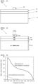
- FIG. 1 shows an example of the inventive spin wave excitation/detection structure 100.
- the spin wave excitation/detection structure 100 can excite the spin wave. Moreover, this can also detect the spin wave.
- the spin wave excitation/detection structure 100 includes a support substrate 12, a conductive film 14 provided on the support substrate 12, an insulating magnetic film 16 provided on the conductive film 14, and a conductive line 18 provided on the insulating magnetic film 16.
- the support substrate 12, the conductive film 14, the insulating magnetic film 16, and the conductive line 18 are laminated in this order.
- the structure can be manufactured by providing and bonding the insulating magnetic film 16 on which the conductive line 18 is film-formed and the support substrate 12 on which the conductive film 14 is film-formed.
- the insulating magnetic film 16 can be epitaxially grown on another growth substrate, not shown in FIG., and then the growth substrate can be removed after the bonding.
- a single crystal of yttrium iron garnet Y 3 Fe 5 O 12 (YIG) grown by liquid epitaxial growth on a nonmagnetic substrate such as gadolinium gallium garnet Gd 3 Ga 5 O 12 (GGG) can be used as the insulating magnetic film 16, in such a case the GGG substrate can be removed by such as grinding.
- YIG yttrium iron garnet Y 3 Fe 5 O 12
- GGG gadolinium gallium garnet Gd 3 Ga 5 O 12
- the insulating magnetic film 16 is preferably made of a magnetic garnet.
- the insulating magnetic film 16 is preferably made of the yttrium iron garnet (YIG).
- the yttrium iron garnet can be a material based on Y 3 Fe 5 O 12 , with a Y portion or a Fe portion being replaced by other elements.
- the thickness of the insulating magnetic film 16 is preferably 10 um or less, more preferably 5 um or less, and particularly preferably 1 um or less. This way, the insulating magnetic film 16 can be as thin as 10 um or less in the inventive spin wave excitation/detection structure 100.
- the conductive film 14 and the conductive line 18 can contain at least any one of copper, aluminum, gold, silver, platinum, iron, transparent conductor, superconductor, graphene, and magnetic material with conductivity. Copper is particularly preferred among these.
- other conductors can be used for the material for the conductive film 14 and the conductive line 18, for example, carbon nanotube or organic conductive material can be used.
- the material of the conductive film 14 and the conductive line 18 is preferred to have higher conductivity than the support substrate 12 or the insulating magnetic film 16.
- the components of the conductive film 14 and the conductive line 18 may be the same or different.
- the conductive line 18 preferably has a thickness of 1 um or less and a width of 5 um or less.
- a thickness of 0.5 um or less is even more preferable, and 0.1 um or less is particularly preferable.
- a width of 2 um or less is even more preferable, and 0.5 um or less is particularly preferable.
- a lower limit of the thickness of the conductive line 18 is not particularly limited; however, if the thickness is too thin, the line is separated and split, and conductivity cannot be maintained, thus, 0.01 um or more is preferable.
- one conductive line 18 of the upper portion is sufficient. However, the lines may be two or more.
- the conductive film 14 preferably has a thickness of 1 um or less.
- the thickness is even more preferably 0.5 um or less, and 0.1 um or less is particularly preferable.
- a lower limit of the thickness of the conductive film 14 is not particularly limited; however, if the thickness is too thin, the film is separated and split, and conductivity cannot be maintained. Thus, 0.01 um or more is preferable.
- the support substrate 12 can be at least any one of a silicon substrate, a dielectric substrate, a conductive substrate, an insulating substrate, a magnetic substrate, a nonmagnetic substrate, a wood substrate, and a stone substrate.
- various support substrates can be used.
- the silicon substrate can be obtained inexpensively and of excellent quality and is preferred as the support substrate 12.
- the insulating substrate glass, quartz, sapphire, aluminum nitride, and alumina, for example, can be exemplified.
- the nonmagnetic substrate a paramagnetic garnet substrate can also be used.
- a thickness of support substrate 12 is preferably 100 um or more and 500 um or less.
- the structure has high mechanical strength and easier handling; moreover, when the support substrate 12 has a thickness of 500 um or less, sufficient mechanical strength can be secured in the structure and is adequate.
- Measurements of a component of the inventive spin wave excitation/detection structure 100 are preferably as enumerated above and can be miniaturized.
- the inventive spin wave excitation/detection structure is expected to become an indispensable component as an excitation structure of the spin wave (a conversion element between electricity and the spin wave) in a spin wave computer, which is said to create a next-generation CPU.
- the spin wave is a phase wave that propagates with an electron in a state of being fixed in place.
- a loss called a Joule heating loss that is supposed to be generated by charge transfer is zero.
- YIG in particular, is an insulator and does not generate an eddy current because of a magnetic oxide material.
- the spin wave has no loss in theory within both elements of a stationary electric current and an eddy current and has the potential to replace all of the wiring, and logic elements, such as NAND or NOR, that CMOS has realized. That is to say, the realizability of a cold computer without heat generation is expected in combination with nanotechnology.
- a ripple effect of the inventive spin wave excitation/detection structure toward related fields includes the following.
- the ripple effect affects all fields where computers are currently used, and device fields where such as CPUs and other arithmetic elements are mounted.
- device fields where such as CPUs and other arithmetic elements are mounted.
- useful in this regard is a situation where the computer is required at a millimeter or a micrometer scale.
- a sensor and a microchip which are increasingly used in a mobile device, a wearable device, and such as household appliances, are included.
- the spin wave is the same as a microwave in light of a responsive wave of the order of GHz; however, a conversion to the wave propagating into the magnetic field makes a wavelength shorten in the order of a hundredfold or more. Considering this from the device (the element) size, this means that an entire chip can be made a hundredfold smaller. Conventionally, the miniaturization of an analog high-frequency device has not progressed much, and the device has a size far from being portable. Therefore, the realization of spin wave devices, including a spin wave phase modulation element, is expected to lead to the miniaturization of a high-frequency device.
- a structure having a conventional structure, in FIG. 4 was manufactured.
- a dielectric substrate 22 had a thickness of 500 ⁇ m
- a copper film 24 had a thickness of 10 um
- a YIG film 26 had a thickness of 10 um
- a copper line 28 had a thickness of 10 um and a width of 10 um.
- the parameters for each material were as follows.
- a spin wave spectrum obtained from a spin wave excitation/detection structure shown in FIG. 4 , was calculated.
- a "conventional structure" in FIG. 3 represents this.
- a spin wave excitation/detection structure in FIG. 2 was manufactured.
- the structure in FIG. 2 prescribed each material of the structure in FIG. 1 and had a dimension shown in FIG. 2 .
- a parameter of each material is shown below.
- Components Materials Parameters Insulating magnetic film YIG Relative permittivity: 15.3 Saturation magnetization: 1800 Gauss Damping constant : 2.
- the spin wave intensity of Example 1 is 15 times larger than a conventional structure of Comparative Example 1, the bandwidth is 8 times larger, and the performance index is 6 times larger, indicating significant improvement and usefulness.
Landscapes
- Physics & Mathematics (AREA)
- Condensed Matter Physics & Semiconductors (AREA)
- General Physics & Mathematics (AREA)
- Hall/Mr Elements (AREA)
- Waveguides (AREA)
Abstract
Description
- The present invention relates to a spin wave excitation/detection structure.
- With explosive increase in an amount of information handled by such as a recent internet, acceleration of a CPU, acceleration of intermediate and long-range communication thanks to RF (high frequency) and optical communication, increase in a data storage capacity, and miniaturization of each part have been developed rapidly. However, an improvement in a processing speed has bottlenecks in that (1) a heat generation problem due to performance improvement by further miniaturization is approaching physical limitation, (2) a development rate of data communication speed between the CPU and a memory (Latency) is slowing down. Concerning the above-described problem (1), replacement to a carrier with low power consumption has been called for. The above-described problem (2) has also become conspicuous, along with a recent development of peripheral technology.
- For example, in a sensor group that can detect sensation at a comparable level with a human being (so-called artificial skin), if access by using a conventional electric device is enabled, the number of transistors becomes enormous, a control unit is enlarged, and a communication delay is caused at the same time. Moreover, regarding a three-dimensional display with high resolution for a medical field and an entertainment field, an expansion of a viewing angle (secured at approximately 45 degrees) allows multiple people to watch simultaneously. On the other hand, when this display is configured by an electric device, the number of transistors is still enormous. Consequently, communication delay or heat generation from a wiring cannot be ignored, thus, burnt out of the wiring or an unstable operation due to heat generated is concerned.
- Thus, with an increasing number of situations where large numbers of elements are required and a rapid increase in the degree of integration, a CMOS-based system has become the bottleneck of an entire application regarding speed and miniaturization.
- Regarding such a problem of a system in which a conventional CMOS is used, technology attempts to solve this problem using a spin wave.
- The spin wave (spin wave) is a phase wave generated by magnetization (spin) in a magnetic material. This wave is also called a magnetostatic wave (magnetostatic wave). In the magnetic material, a large number of spins are contained, as shown in
FIG. 6 . The plane where the timing (phase) of the rotation of these spins is aligned creates a wavefront. When the wavefront propagates, information is transmitted. This is the spin wave, and information can be transmitted without a charge transfer. The spin wave is a phenomenon related only to the magnetism of a material and not to the electrical properties. In other words, this wave propagates as long as the magnetic material is used, regardless of whether an electric conductor or an insulator is used. Consequently, by using the insulator, the wiring, in which an electric current does not flow through, but the spin wave propagates, can be produced. Moreover, this spin wave is the wave having a GHz (gigahertz) band, thus fast enough for information processing. - In this way, since the spin wave is a method to transmit information with no charge transfer being required, thus has attracted attention as a potential information processing device with ultra-low power consumption in the next generation. Basic logic circuits such as an XNOR circuit [see Non Patent Document 1], an AND circuit, and an OR circuit [see Non Patent Document 2] are already in the research stage of being demonstrated. The basic elements have been demonstrated, thus, more complex and practical circuits and applications are proposed, demonstrated, and patented in the present situation. Recently, a study has disclosed a computation showing that a compact address decoder can be manufactured by using the spin wave (see Patent Document 1). In addition to the development of functionality, miniaturization of size has also progressed. Miniaturization to a micrometer and a nanoscale is considered to move on.
- Several methods exist to generate the spin wave, but currently, a technique to generate the spin wave using the electric current is mainstream.
-
Patent Document 2 discloses the spin wave excitation structure of a coplanar waveguide type (a complete type in one layer). This spin wave excitation structure (an antenna) is a type in which a copper line for a signal level and a copper line for a ground level are formed in one layer. A structure, as disclosed inPatent Document 2, allows an input of high-frequency electrical signals. As described above, this structure is called the coplanar waveguide structure and is a widely known structure. An antenna part can be produced in a completed single layer and can be minimized to a nanometer scale, thus widely used. However, the spin wave (magnetostatic wave) that can be generated has a problem in which the frequency bandwidth is narrow. -
Patent Document 3 discloses the spin wave excitation structure of a microstrip line type. The microstrip line is a structure in which a single current-flowing copper line (signal level) is placed on a medium through which the spin wave propagates, and a ground level is placed below the medium (YIG (yttrium iron garnet) is shown as an example in Patent Document 3) through which the spin wave propagates. - The microstrip line type structure, disclosed in
Patent Document 3, has an advantage where the spin wave that can be generated has a wide band. On the other hand, the signal level and the ground level step over YIG and form a multilevel structure, thus, the integration is difficult to achieve. - With advancement of the miniaturization and integration, as making the microstrip line narrower, a distance between the signal level and the ground level (= a thickness of YIG) is intact, thus, a high-frequency rotating magnet field cannot be produced well in the medium in which the spin wave propagates, and thus an intensity of the spin wave decreases. When the signal level and ground level are close, and the more YIG is interposed between, the spin wave intensity that can be excited is increased.
- When making the microstrip line narrower, thinning YIG simultaneously can be considered a technique to maintain the intensity of the spin wave. However, when YIG has a thickness of 1 micrometer or less, YIG is unable to self-support (YIG may crack). Consequently, YIG is typically handled in a state of being placed on a substrate having a thickness of 100 micrometer class, thus, a study of structure is conducted within such range.
- Specifically, a conductor (often the copper line) called the microstrip line (Microstrip line) is used, as shown in
FIG. 5(a) . Copper is film-formed on an entire surface of a Teflon (registered trademark) substrate of a lower side of the Teflon (registered trademark) substrate (Teflon substrate). The thickness of the copper film is about 10 um. The copper line on the Teflon (registered trademark) substrate has a width of about 10 um and a thickness of about 10 um, too. When an electric current is applied to this line, a rotating magnetic field that rotates at a speed of about GHz is generated around this copper line. Under a condition when a direct current magnetic field is applied to a region where this rotating magnetic field is generated, and if a magnetic insulator (a material called YIG inFIG. 5(a) ) is placed on the region, the spin wave is excited by the rotating magnetic field. As a result, the spin wave is propagated from one microstrip line (an input microstrip line, Input microstrip line) to another microstrip line (an output microstrip line, Output microstrip line). At the point of the output microstrip line, reversely, the rotating magnetic field generated by the spin wave generates an electric current in the microstrip line. In other words, making the electric current flow excites the spin wave. Then, the propagation of the spin wave is generated, and then an operation is performed during the propagation, and then a result of the operation is propagated. Then, a conversion of the spin wave to the electric current is performed, and the result is detected as an electric signal. This means that a spin wave propagation spectrum can be obtained, as shown in the "with magnetic field" line inFIG. 5(b) . "Without YIG" inFIG. 5(b) shows a spectrum without YIG in a structure inFIG. 5(a) , "without magnetic field" inFIG. 5(b) shows a spectrum when the direct current magnetic field is not applied in a structure inFIG. 5(a) . Moreover, referring toFIG. 5(a) , the part of the input microstrip line is the spin wave excitation structure, and the part of the output microstrip line is the spin wave detection structure. -
- Patent Document 1:
JP 2017-162937 A - Patent Document 2:
JP 2006-504345 A - Patent Document 3:
JP H1-91514 A - Non Patent Document 1: Taichi Goto, Takuya Yoshimoto, Bungo Iwamoto, Kei Shimada, Caroline A. Ross, Koji Sekiguchi, Alexander B. Granovsky, Yuichi Nakamura, Hironaga Uchida and Mitsuteru Inoue, "Three port logic gate using forward volume spin wave interference in a thin yttrium iron garnet film", Scientific Reports, 9, 16472 (2019/11/11).
- Non Patent Document 2: Naoki Kanazawa, Taichi Goto, Koji Sekiguchi, Alexander B. Granovsky, Caroline A. Ross, Hiroyuki Takagi, Yuichi Nakamura, Hironaga Uchida and Mitsuteru Inoue, "The role of Snell's law for a magnonic majority gate", Scientific Reports, 7, 7898 (2017/08/11).
- As described above, spin wave devices, attracting attention as the latest information processing devices, also have a problem. This is a low intensity of a spin wave.
- A currently used spin wave excitation structure using electricity (also known as a transducer or an antenna) (which can also be a spin-wave detection structure, as described above) is shown in
FIG. 4 when a cross-sectional view is illustrated. A conventional spin wave excitation/detection structure 200 has a structure in which acopper film 24 is under adielectric substrate 22, and aYIG film 26 with gadoliniumgallium garnet substrate 25 is mounted on acopper line 28. This is not suited for miniaturization and integration. This is because if the miniaturization is achieved by a method according to simple scale down, an excitation efficiency becomes significantly low, and a bandwidth becomes significantly narrow. - The present invention has been made in view of the above-described problem. An object of the present invention is to provide a spin wave excitation/detection structure having a structure with high strength, the spin wave that can be excited with high intensity, and the spin wave that can be excited with broad frequency bandwidth.
- To achieve the object, the present invention provides a spin wave excitation/detection structure to excite and detect a spin wave, comprising:
- a support substrate;
- a conductive film provided on the support substrate;
- an insulating magnetic film provided on the conductive film; and
- a conductive line provided on the insulating magnetic film.
- Such a spin wave excitation/detection structure has a structure with high strength, the spin wave that can be excited with high intensity. Moreover, frequency bandwidth of the spin wave that can be excited is broad.
- Note that the insulating magnetic film is preferably a magnetic garnet. Furthermore, the insulating magnetic film is preferably an yttrium iron garnet.
- By using these kinds of insulating magnetic films, an excellent spin wave can be excited. In addition, the detection of the spin wave can also be performed without any problem.
- In addition, the conductive film and the conductive line can contain at least any one of copper, aluminum, gold, silver, platinum, iron, transparent conductor, superconductor, graphene, and magnetic material with conductivity.
- In the inventive spin wave excitation/detection structure, the above kinds of conductors, as well as copper, can be used as a conductor component.
- Furthermore, the support substrate can be at least any one of a silicon substrate, a dielectric substrate, a conductive substrate, an insulating substrate, a magnetic substrate, a nonmagnetic substrate, a wood substrate, and a stone substrate.
- In the inventive spin wave excitation/detection structure, the silicon substrate or other substrates of the kinds described above can be used for the support substrate.
- In addition, the insulating magnetic film preferably has a thickness of 10 um or less.
- Furthermore, the conductive line preferably has a thickness of 1 um or less and a width of 5 um or less.
- Additionally, the conductive film preferably has a thickness of 1 um or less.
- Moreover, the support substrate preferably has a thickness of 100 um or more and 500 um or less.
- Dimensions of a component of the inventive spin wave excitation/detection structure are preferably like the above and can be miniaturized.
- The inventive spin wave excitation/detection structure has a structure with high strength, and the spin wave that can be excited with high intensity. In addition, a frequency bandwidth of the spin wave that can be excited is broad. In more detail, the inventive spin wave excitation/detection structure has the insulating magnetic film and the support substrate via the conductive film and a characteristic of a wide excitation bandwidth of the microstrip line. In addition, the structure has the signal level and the ground level nearby, and the insulating magnetic film sandwiched between these levels as a propagating region for the excited spin wave, thus, the intensity of the spin wave excited is high. Moreover, the insulating magnetic film is bonded to the support substrate via the conductive film, which has an effect on high mechanical strength of the structure and an ability for handling.
-
-
FIG. 1 is a view illustrating an example of a schematic cross-sectional view of a spin wave excitation/detection structure according to the present invention. -
FIG. 2 is a view illustrating a schematic cross-sectional view of a spin wave excitation/detection structure used in Example. -
FIG. 3 is a graph showing spin wave propagation spectra in Example and Comparative Example, respectively. -
FIG. 4 is a view illustrating a schematic cross-sectional view of a spin wave excitation/detection structure used in Comparative Example. -
FIG. 5(a) is a view illustrating a perspective view of a spin wave excitation/detection structure of a conventional microstrip type, and (b) is spin wave propagation spectra in this structure. -
FIG. 6 is a view illustrating a schematic view to describe a spin wave. - Hereinafter, embodiments of the present invention will be described. However, the present invention is not limited thereto.
- As described above, a currently used spin wave excitation structure (also known as a transducer or an antenna) using electricity, shown in
FIG. 4 , is not suitable for miniaturization and integration. Since an excitation efficiency becomes extremely low and bandwidth becomes extremely narrow when miniaturization is done by a simple scaling down method. Specifically, when acopper line 28 of the upper portion is made thinner and narrower for miniaturization and integration, an intensity of a spin wave decreases. This is because thecopper line 28 of the upper portion and acopper film 24 of the lower portion are too far. Consequently, a technique to make adielectric substrate 22 portion thinner comes to mind, but this makes a rotating magnetic field unable to generate in aYIG film 26 of the upper portion. Therefore, theYIG film 26 needs to be located between thecopper line 28 of the upper portion and thecopper film 24 of the lower portion. Furthermore, if a sample is too thin, the sample falls apart thus a substrate (the dielectric substrate 22) is necessary. - The present inventors devised a structure shown in
FIG. 1 to be useful, based on a problem with the conventional spin wave excitation/detection structure 200 shown inFIG. 4 , and found out the usefulness through calculations. Consequently, the following inventive structure is proposed. -
FIG. 1 shows an example of the inventive spin wave excitation/detection structure 100. The spin wave excitation/detection structure 100 can excite the spin wave. Moreover, this can also detect the spin wave. The spin wave excitation/detection structure 100 includes asupport substrate 12, aconductive film 14 provided on thesupport substrate 12, an insulatingmagnetic film 16 provided on theconductive film 14, and aconductive line 18 provided on the insulatingmagnetic film 16. In other words, thesupport substrate 12, theconductive film 14, the insulatingmagnetic film 16, and theconductive line 18 are laminated in this order. - With the
conductive line 18 of the upper portion as an electric signal level and theconductive film 14 of the lower portion as an electric ground level, supplying a high-frequency signal in the gigahertz band excites the spin wave within the insulatingmagnetic film 16. - When the spin wave excitation/detection structure 100 shown in
FIG. 1 is manufactured, for example, the structure can be manufactured by providing and bonding the insulatingmagnetic film 16 on which theconductive line 18 is film-formed and thesupport substrate 12 on which theconductive film 14 is film-formed. For example, a YIG on which a Cu line is film-formed and a Si substrate on which a Cu film is film-formed are provided and then bonded, this allows the manufacturing of the inventive structure. Moreover, the insulatingmagnetic film 16 can be epitaxially grown on another growth substrate, not shown in FIG., and then the growth substrate can be removed after the bonding. For example, a single crystal of yttrium iron garnet Y3Fe5O12 (YIG) grown by liquid epitaxial growth on a nonmagnetic substrate such as gadolinium gallium garnet Gd3Ga5O12 (GGG) can be used as the insulatingmagnetic film 16, in such a case the GGG substrate can be removed by such as grinding. - At this point, in the spin wave excitation/detection structure 100 in
FIG. 1 , the insulatingmagnetic film 16 is preferably made of a magnetic garnet. In particular, the insulatingmagnetic film 16 is preferably made of the yttrium iron garnet (YIG). Furthermore, the yttrium iron garnet can be a material based on Y3Fe5O12, with a Y portion or a Fe portion being replaced by other elements. By using the magnetic garnet, especially the yttrium iron garnet, as the insulatingmagnetic film 16, an excellent spin wave can be excited. Moreover, the detection of the spin wave can be performed without any problems. The thickness of the insulatingmagnetic film 16 is preferably 10 um or less, more preferably 5 um or less, and particularly preferably 1 um or less. This way, the insulatingmagnetic film 16 can be as thin as 10 um or less in the inventive spin wave excitation/detection structure 100. - In the spin wave excitation/detection structure 100 in
FIG. 1 , theconductive film 14 and theconductive line 18 can contain at least any one of copper, aluminum, gold, silver, platinum, iron, transparent conductor, superconductor, graphene, and magnetic material with conductivity. Copper is particularly preferred among these. Moreover, other conductors can be used for the material for theconductive film 14 and theconductive line 18, for example, carbon nanotube or organic conductive material can be used. Furthermore, the material of theconductive film 14 and theconductive line 18 is preferred to have higher conductivity than thesupport substrate 12 or the insulatingmagnetic film 16. The components of theconductive film 14 and theconductive line 18 may be the same or different. - Among these, the
conductive line 18 preferably has a thickness of 1 um or less and a width of 5 um or less. A thickness of 0.5 um or less is even more preferable, and 0.1 um or less is particularly preferable. Moreover, a width of 2 um or less is even more preferable, and 0.5 um or less is particularly preferable. Furthermore, a lower limit of the thickness of theconductive line 18 is not particularly limited; however, if the thickness is too thin, the line is separated and split, and conductivity cannot be maintained, thus, 0.01 um or more is preferable. Moreover, oneconductive line 18 of the upper portion is sufficient. However, the lines may be two or more. - In addition, the
conductive film 14 preferably has a thickness of 1 um or less. The thickness is even more preferably 0.5 um or less, and 0.1 um or less is particularly preferable. Moreover, a lower limit of the thickness of theconductive film 14 is not particularly limited; however, if the thickness is too thin, the film is separated and split, and conductivity cannot be maintained. Thus, 0.01 um or more is preferable. - Additionally, in the spin wave excitation/detection structure 100 in
FIG.1 , thesupport substrate 12 can be at least any one of a silicon substrate, a dielectric substrate, a conductive substrate, an insulating substrate, a magnetic substrate, a nonmagnetic substrate, a wood substrate, and a stone substrate. In this way, various support substrates can be used. Among these, the silicon substrate can be obtained inexpensively and of excellent quality and is preferred as thesupport substrate 12. As for the insulating substrate, glass, quartz, sapphire, aluminum nitride, and alumina, for example, can be exemplified. Regarding the nonmagnetic substrate, a paramagnetic garnet substrate can also be used. A thickness ofsupport substrate 12 is preferably 100 um or more and 500 um or less. When thesupport substrate 12 has a thickness of 100 um or more, the structure has high mechanical strength and easier handling; moreover, when thesupport substrate 12 has a thickness of 500 um or less, sufficient mechanical strength can be secured in the structure and is adequate. - Measurements of a component of the inventive spin wave excitation/detection structure 100 are preferably as enumerated above and can be miniaturized.
- As described above, the inventive spin wave excitation/detection structure is expected to become an indispensable component as an excitation structure of the spin wave (a conversion element between electricity and the spin wave) in a spin wave computer, which is said to create a next-generation CPU.
- The spin wave is a phase wave that propagates with an electron in a state of being fixed in place. Thus, in theory, a loss called a Joule heating loss that is supposed to be generated by charge transfer is zero. Moreover, YIG, in particular, is an insulator and does not generate an eddy current because of a magnetic oxide material. In this way, the spin wave has no loss in theory within both elements of a stationary electric current and an eddy current and has the potential to replace all of the wiring, and logic elements, such as NAND or NOR, that CMOS has realized. That is to say, the realizability of a cold computer without heat generation is expected in combination with nanotechnology.
- A ripple effect of the inventive spin wave excitation/detection structure toward related fields includes the following.
- The ripple effect affects all fields where computers are currently used, and device fields where such as CPUs and other arithmetic elements are mounted. In particular, useful in this regard is a situation where the computer is required at a millimeter or a micrometer scale. For example, a sensor and a microchip, which are increasingly used in a mobile device, a wearable device, and such as household appliances, are included.
- The spin wave is the same as a microwave in light of a responsive wave of the order of GHz; however, a conversion to the wave propagating into the magnetic field makes a wavelength shorten in the order of a hundredfold or more. Considering this from the device (the element) size, this means that an entire chip can be made a hundredfold smaller. Conventionally, the miniaturization of an analog high-frequency device has not progressed much, and the device has a size far from being portable. Therefore, the realization of spin wave devices, including a spin wave phase modulation element, is expected to lead to the miniaturization of a high-frequency device.
- Hereinafter, the present invention will be specifically described with reference to Example and Comparative Example of the present invention. However, the present invention is not limited to these Examples.
- A structure having a conventional structure, in
FIG. 4 , was manufactured. Adielectric substrate 22 had a thickness of 500 µm, acopper film 24 had a thickness of 10 um, aYIG film 26 had a thickness of 10 um, and acopper line 28 had a thickness of 10 um and a width of 10 um. The parameters for each material were as follows.[Table 1] Components Materials Parameters Insulating magnetic film YIG Relative permittivity: 15.3 Saturation magnetization: 1800 Gauss Damping constant : 2.4×10⁻⁴ External magnetic field: range from 500 Oe to 1500 Oe Direction of external magnetic field: from bottom to top of cross-sectional view Conductive film and conductive line Cu Conductivity : 5.96×10⁷ S/m Dielectric substrate Teflon substrate Relative permittivity: 4.4 Dielectric loss Tanδ=0.02 - A spin wave spectrum, obtained from a spin wave excitation/detection structure shown in
FIG. 4 , was calculated. A "conventional structure" inFIG. 3 represents this. - From
FIG. 3 , a spin wave intensity and a spin wave bandwidth were obtained, as shown below, respectively. - · The spin wave intensity: 1.17 Oe (a value of the spin wave intensity at 4.0 GHz, an operating frequency).
- · The spin wave bandwidth: 0.243 GHz (representing a frequency range from 4.0 GHz, the operating frequency, to the frequency when the spin wave intensity reached half value).
- When a value in which these two values are multiplied is defined as a performance index, the index is indicated below:
- · The performance index: 0.285 GHz·Oe
- A spin wave excitation/detection structure in
FIG. 2 , the inventive structure, was manufactured. The structure inFIG. 2 prescribed each material of the structure inFIG. 1 and had a dimension shown inFIG. 2 . A parameter of each material is shown below.[Table 2] Components Materials Parameters Insulating magnetic film YIG Relative permittivity: 15.3 Saturation magnetization: 1800 Gauss Damping constant : 2. 4×10⁻⁴ External magnetic field: Range from 500 Oe to 1500 Oe Direction of external magnetic field: from bottom to top of cross-sectional view Conductive film and conductive line Cu Conductivity : 5.96×10⁷ S /m Support substrate Si substrate Relative permittivity : 12 Conductivity: 50 S/m FIG. 2 was calculated. "Structure of the present invention" inFIG. 3 indicated this. - From
FIG. 3 , a spin wave intensity and a spin wave bandwidth were able to be obtained. Each was as follows. - · The spin wave intensity: 15.3 Oe (a value of the spin wave intensity at 4.0 GHz, an operating frequency).
- · The spin wave bandwidth: 1.62 GHz (representing a frequency range from 4.0 GHz, the operating frequency, to the frequency when the spin wave intensity reached half value).
- When a value in which these two values are multiplied is defined as a performance index, the index is indicated below:
- · The performance index: 24.8 GHz·Oe
- The spin wave intensity of Example 1 is 15 times larger than a conventional structure of Comparative Example 1, the bandwidth is 8 times larger, and the performance index is 6 times larger, indicating significant improvement and usefulness.
- It should be noted that the present invention is not limited to the above-described embodiments. The embodiments are just examples, and any examples that have substantially the same feature and demonstrate the same functions and effects as those in the technical concept disclosed in claims of the present invention are included in the technical scope of the present invention.
Claims (9)
- A spin wave excitation/detection structure to excite and detect a spin wave, comprising:a support substrate;a conductive film provided on the support substrate;an insulating magnetic film provided on the conductive film; anda conductive line provided on the insulating magnetic film.
- The spin wave excitation/detection structure according to claim 1, wherein
the insulating magnetic film is a magnetic garnet. - The spin wave excitation/detection structure according to claim 2, wherein
the insulating magnetic film is an yttrium iron garnet. - The spin wave excitation/detection structure according to any one of claims 1 to 3, wherein
the conductive film and the conductive line contain at least any one of copper, aluminum, gold, silver, platinum, iron, transparent conductor, superconductor, graphene, and magnetic material with conductivity. - The spin wave excitation/detection structure according to any one of claims 1 to 4, wherein
the support substrate is at least any one of a silicon substrate, a dielectric substrate, a conductive substrate, an insulating substrate, a magnetic substrate, a nonmagnetic substrate, a wood substrate, and a stone substrate. - The spin wave excitation/detection structure according to any one of claims 1 to 5, wherein
the insulating magnetic film has a thickness of 10 um or less. - The spin wave excitation/detection structure according to any one of claims 1 to 6, wherein
the conductive line has a thickness of 1 um or less and a width of 5 um or less. - The spin wave excitation/detection structure according to any one of claims 1 to 7, wherein
the conductive film has a thickness of 1 um or less. - The spin wave excitation/detection structure according to any one of claims 1 to 8, wherein
the support substrate has a thickness of 100 um or more and 500 um or less.
Applications Claiming Priority (2)
| Application Number | Priority Date | Filing Date | Title |
|---|---|---|---|
| JP2021123390A JP7852849B2 (en) | 2021-07-28 | 2021-07-28 | Spin wave excitation detection structure |
| PCT/JP2022/028656 WO2023008383A1 (en) | 2021-07-28 | 2022-07-25 | Spin wave excitation/detection structure |
Publications (2)
| Publication Number | Publication Date |
|---|---|
| EP4379814A1 true EP4379814A1 (en) | 2024-06-05 |
| EP4379814A4 EP4379814A4 (en) | 2025-06-25 |
Family
ID=85086993
Family Applications (1)
| Application Number | Title | Priority Date | Filing Date |
|---|---|---|---|
| EP22849444.9A Pending EP4379814A4 (en) | 2021-07-28 | 2022-07-25 | Spin wave excitation/detection structure |
Country Status (6)
| Country | Link |
|---|---|
| US (1) | US20240272250A1 (en) |
| EP (1) | EP4379814A4 (en) |
| JP (1) | JP7852849B2 (en) |
| CN (1) | CN117716516A (en) |
| CA (1) | CA3227692A1 (en) |
| WO (1) | WO2023008383A1 (en) |
Family Cites Families (10)
| Publication number | Priority date | Publication date | Assignee | Title |
|---|---|---|---|---|
| JPH0758843B2 (en) * | 1987-10-01 | 1995-06-21 | 株式会社村田製作所 | Magnetostatic wave device |
| FR2846472B1 (en) | 2002-10-28 | 2007-04-20 | Commissariat Energie Atomique | MAGNETOSTATIC WAVE DEVICES BASED ON METAL THIN FILMS, PROCESS FOR MANUFACTURING AND APPLICATION TO MICROWAVE FREQUENCY SIGNAL PROCESSING DEVICES |
| JP5339272B2 (en) | 2008-06-05 | 2013-11-13 | 国立大学法人東北大学 | Spintronic device and information transmission method |
| WO2009151000A1 (en) | 2008-06-12 | 2009-12-17 | 学校法人 慶應義塾 | Thermoelectric conversion element |
| JP6143051B2 (en) | 2012-10-19 | 2017-06-07 | 国立大学法人東北大学 | Spintronics device |
| JP5649704B1 (en) | 2013-09-18 | 2015-01-07 | 株式会社東芝 | Magnetic recording device |
| US9929338B2 (en) * | 2015-10-09 | 2018-03-27 | The Regents Of The University Of California | Spin current devices and methods of fabrication thereof |
| JP6706838B2 (en) | 2016-03-08 | 2020-06-10 | 国立大学法人豊橋技術科学大学 | Spin wave circuit and address encoder and address decoder |
| CN110299446B (en) * | 2019-06-24 | 2021-03-26 | 华中科技大学 | Electric control magneton valve structure based on acoustic wave excitation |
| CN112968058B (en) * | 2021-02-04 | 2022-07-26 | 电子科技大学 | Ion-regulated spin wave transistor and preparation method thereof |
-
2021
- 2021-07-28 JP JP2021123390A patent/JP7852849B2/en active Active
-
2022
- 2022-07-25 CN CN202280052710.1A patent/CN117716516A/en active Pending
- 2022-07-25 CA CA3227692A patent/CA3227692A1/en active Pending
- 2022-07-25 WO PCT/JP2022/028656 patent/WO2023008383A1/en not_active Ceased
- 2022-07-25 EP EP22849444.9A patent/EP4379814A4/en active Pending
- 2022-07-25 US US18/292,195 patent/US20240272250A1/en active Pending
Also Published As
| Publication number | Publication date |
|---|---|
| WO2023008383A1 (en) | 2023-02-02 |
| EP4379814A4 (en) | 2025-06-25 |
| JP2023018973A (en) | 2023-02-09 |
| US20240272250A1 (en) | 2024-08-15 |
| CN117716516A (en) | 2024-03-15 |
| JP7852849B2 (en) | 2026-04-28 |
| CA3227692A1 (en) | 2023-02-02 |
Similar Documents
| Publication | Publication Date | Title |
|---|---|---|
| Fischer et al. | Experimental prototype of a spin-wave majority gate | |
| US20190042968A1 (en) | Quantum circuit assemblies with triaxial cables | |
| Khitun et al. | Feasibility study of logic circuits with a spin wave bus | |
| CN107845852A (en) | A kind of composite substrate formula microstrip circulator | |
| Lutsev et al. | Spin-wave filters based on thin Y3Fe5O12 films on Gd3Ga5O12 and Si substrates for microwave applications | |
| Geiler et al. | Multiferroic heterostructure fringe field tuning of meander line microstrip ferrite phase shifter | |
| JP2006504345A (en) | Magnetostatic devices based on thin metal films, methods for manufacturing the same, and applications to devices for processing microwave signals | |
| CN107146935A (en) | A kind of quantum circulator based on asymmetric annular chamber | |
| Yang et al. | Microstrip-line resonator with broadband, circularly polarized, uniform microwave field for nitrogen vacancy center ensembles in diamond | |
| How et al. | Theory and experiment of thin-film junction circulator | |
| Mori et al. | Broadband excitation of spin wave using microstrip line antennas for integrated magnonic devices | |
| Montagu et al. | Spin polarised quantum conductance in 1D channels | |
| WO2010097997A1 (en) | Magnetic oscillation element | |
| US20240272250A1 (en) | Spin wave excitation/detection structure | |
| Zheng et al. | Spin wave propagation in uniform waveguide: effects, modulation and its application | |
| Serha et al. | Magnetic Materials for Quantum Magnonics | |
| US20240341198A1 (en) | Method for manufacturing spin wave excitation/detection structure | |
| Wu et al. | A three-terminal spin-wave device for logic applications | |
| Chao et al. | Millimeter wave complementary metal-oxide-semiconductor on-chip hexagonal ferrite circulator | |
| Wang et al. | Frequency-selective coherent propagating spin waves induced by localized perpendicular magnetic anisotropy nanofilm stack | |
| Li et al. | Terahertz monolithic integrated waveguide transmission lines based on wide bandgap semiconductor materials | |
| Khitun et al. | Efficiency of spin-wave bus for information transmission | |
| Wang et al. | From nanoelectronics to nano-spintronics | |
| Neumaier et al. | High frequency graphene transistors: can a beauty become a cash cow? | |
| CN118263638A (en) | Spin wave phase shifter based on magneton transfer torque regulation and control |
Legal Events
| Date | Code | Title | Description |
|---|---|---|---|
| STAA | Information on the status of an ep patent application or granted ep patent |
Free format text: STATUS: THE INTERNATIONAL PUBLICATION HAS BEEN MADE |
|
| PUAI | Public reference made under article 153(3) epc to a published international application that has entered the european phase |
Free format text: ORIGINAL CODE: 0009012 |
|
| STAA | Information on the status of an ep patent application or granted ep patent |
Free format text: STATUS: REQUEST FOR EXAMINATION WAS MADE |
|
| 17P | Request for examination filed |
Effective date: 20240125 |
|
| AK | Designated contracting states |
Kind code of ref document: A1 Designated state(s): AL AT BE BG CH CY CZ DE DK EE ES FI FR GB GR HR HU IE IS IT LI LT LU LV MC MK MT NL NO PL PT RO RS SE SI SK SM TR |
|
| DAV | Request for validation of the european patent (deleted) | ||
| DAX | Request for extension of the european patent (deleted) | ||
| REG | Reference to a national code |
Ref country code: DE Ref legal event code: R079 Free format text: PREVIOUS MAIN CLASS: H01L0029820000 Ipc: H03B0015000000 |
|
| A4 | Supplementary search report drawn up and despatched |
Effective date: 20250527 |
|
| RIC1 | Information provided on ipc code assigned before grant |
Ipc: H03B 15/00 20060101AFI20250521BHEP |