EP4378883A1 - Mems transducer device for high-frequency applications, and manufacturing method - Google Patents
Mems transducer device for high-frequency applications, and manufacturing method Download PDFInfo
- Publication number
- EP4378883A1 EP4378883A1 EP23207483.1A EP23207483A EP4378883A1 EP 4378883 A1 EP4378883 A1 EP 4378883A1 EP 23207483 A EP23207483 A EP 23207483A EP 4378883 A1 EP4378883 A1 EP 4378883A1
- Authority
- EP
- European Patent Office
- Prior art keywords
- transducer
- conductive
- conductive coupling
- forming
- coupling elements
- Prior art date
- Legal status (The legal status is an assumption and is not a legal conclusion. Google has not performed a legal analysis and makes no representation as to the accuracy of the status listed.)
- Granted
Links
Images






Classifications
-
- H—ELECTRICITY
- H04—ELECTRIC COMMUNICATION TECHNIQUE
- H04R—LOUDSPEAKERS, MICROPHONES, GRAMOPHONE PICK-UPS OR LIKE ACOUSTIC ELECTROMECHANICAL TRANSDUCERS; ELECTRIC HEARING AIDS; PUBLIC ADDRESS SYSTEMS
- H04R17/00—Piezoelectric transducers; Electrostrictive transducers
- H04R17/02—Microphones
-
- B—PERFORMING OPERATIONS; TRANSPORTING
- B81—MICROSTRUCTURAL TECHNOLOGY
- B81C—PROCESSES OR APPARATUS SPECIALLY ADAPTED FOR THE MANUFACTURE OR TREATMENT OF MICROSTRUCTURAL DEVICES OR SYSTEMS
- B81C1/00—Manufacture or treatment of devices or systems in or on a substrate
- B81C1/00015—Manufacture or treatment of devices or systems in or on a substrate for manufacturing microsystems
- B81C1/00222—Integrating an electronic processing unit with a micromechanical structure
- B81C1/00238—Joining a substrate with an electronic processing unit and a substrate with a micromechanical structure
-
- H—ELECTRICITY
- H04—ELECTRIC COMMUNICATION TECHNIQUE
- H04R—LOUDSPEAKERS, MICROPHONES, GRAMOPHONE PICK-UPS OR LIKE ACOUSTIC ELECTROMECHANICAL TRANSDUCERS; ELECTRIC HEARING AIDS; PUBLIC ADDRESS SYSTEMS
- H04R31/00—Apparatus or processes specially adapted for the manufacture of transducers or diaphragms therefor
- H04R31/006—Interconnection of transducer parts
-
- B—PERFORMING OPERATIONS; TRANSPORTING
- B81—MICROSTRUCTURAL TECHNOLOGY
- B81C—PROCESSES OR APPARATUS SPECIALLY ADAPTED FOR THE MANUFACTURE OR TREATMENT OF MICROSTRUCTURAL DEVICES OR SYSTEMS
- B81C2203/00—Forming microstructural systems
- B81C2203/07—Integrating an electronic processing unit with a micromechanical structure
- B81C2203/0785—Transfer and j oin technology, i.e. forming the electronic processing unit and the micromechanical structure on separate substrates and joining the substrates
- B81C2203/0792—Forming interconnections between the electronic processing unit and the micromechanical structure
-
- H—ELECTRICITY
- H04—ELECTRIC COMMUNICATION TECHNIQUE
- H04R—LOUDSPEAKERS, MICROPHONES, GRAMOPHONE PICK-UPS OR LIKE ACOUSTIC ELECTROMECHANICAL TRANSDUCERS; ELECTRIC HEARING AIDS; PUBLIC ADDRESS SYSTEMS
- H04R2201/00—Details of transducers, loudspeakers or microphones covered by H04R1/00 but not provided for in any of its subgroups
- H04R2201/003—Mems transducers or their use
-
- H—ELECTRICITY
- H04—ELECTRIC COMMUNICATION TECHNIQUE
- H04R—LOUDSPEAKERS, MICROPHONES, GRAMOPHONE PICK-UPS OR LIKE ACOUSTIC ELECTROMECHANICAL TRANSDUCERS; ELECTRIC HEARING AIDS; PUBLIC ADDRESS SYSTEMS
- H04R2400/00—Loudspeakers
- H04R2400/01—Transducers used as a loudspeaker to generate sound aswell as a microphone to detect sound
Definitions
- the present invention relates to a micro-electro-mechanical (MEMS) device, in particular to an electroacoustic transducer device, and to a manufacturing method of the micro-electro-mechanical device.
- MEMS micro-electro-mechanical
- an ultrasound sensor comprises, in addition to an electroacoustic transducer, a circuitry for driving the transducer, as well as for amplifying the electrical signals generated by the same transducer following the reception of acoustic echo signals.
- the transducer therefore acts as both an acoustic emitter and an acoustic receiver, in different time periods.
- stimulus acoustic signals and response acoustic signals to indicate, respectively, acoustic signals (or beams) transmitted by the transducer and acoustic signals (or beams) impinging on the transducer, for example following the reflection of the stimulus acoustic signals by an obstacle
- the need is known, for example in the ultrasound field, to be able to focus the stimulus acoustic signals.
- the transducers In order to increase performances, in particular as regards echo amplification, the transducers, typically formed by corresponding MEMS devices arranged according to a matrix, need to be arranged as close as possible to the electronic circuitry, and in particular to the part of electronic circuitry responsible for amplifying the electrical signals generated by the transducers.
- this need clashes with the high number of transducers (in the order of thousands) typically used.
- each transducer is coupled to a respective application-specific integrated circuit (ASIC), which forms the driver circuit and the receiver associated with the transducer, thousands of connections present between the transducers and the ASIC circuits connected thereto need to be dealt with, by controlling the delays introduced by the different channels (each channel being understood as formed by a transducer, the corresponding driver circuit and the corresponding receiver), as well as the jitter present between the different channels.
- ASIC application-specific integrated circuit
- manufacturing processes are currently known which provide for processing a first and a second semiconductive wafer, so as to form, in the first wafer, a plurality of transducers, as well as to form, in the second wafer, a plurality of ASIC circuits. Subsequently, the first and the second wafers are coupled to each other, such that the transducers are coupled to the corresponding ASIC circuits.
- This process is characterized by a reduced flexibility, since it provides for the adoption of a single manufacturing technology for both the driver circuits and the reception circuits. Furthermore, this manufacturing process does not allow the ASIC circuits to be tested until the same process has been ended. Again, this manufacturing process requires that the pitch of the electrical connection pads in the first and the second wafers be the same.
- the patent document EP3599217 discusses that, to increase the performances and in particular as regards the echo amplification, it is advisable that the transducers, (typically formed by corresponding MEMS devices arranged according to a matrix) are arranged as close as possible to the electronic circuitry, and in particular to the part of the electronic circuitry which has the function of amplifying the electrical signals generated by the transducers.
- the authors of this patent document provide a manufacturing process for MEMS devices which partially overcomes the drawbacks of the prior art.
- the known manufacturing process does not allow to manufacture broadband PMUTs above 4 MHz due to some process limitations, including for example the minimum cavity-cavity distance and the minimum thickness of the membrane.
- the aim of the present invention is therefore to provide a MEMS device and a manufacturing method of the MEMS device, to at least partially overcome the drawbacks of the prior art.
- a MEMS device and a manufacturing method of the MEMS device are provided, as defined in the attached claims.
- Figure 1A shows a portion of a MEMS device 1, particularly an electroacoustic device, even more particularly an ultrasonic transducer device (PMUT), in a triaxial system of axes X, Y, Z orthogonal to each other.
- the view of Figure 1A is in-section on the XZ plane.
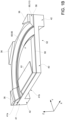
- Figure 1B shows in perspective view a detail of the MEMS device 1 of Figure 1A (some elements are not present, for simplicity of representation and better clarity), in the triaxial system XYZ.
- the electroacoustic device 1 comprises a first and a second die 2, 4, having a first and a second integrated circuit 6, 8, respectively, formed therein, formed for example by known ASIC circuits.
- Each of the first and the second integrated circuits 6, 8 comprises a respective transmission circuit and a respective reception circuit of respective actuation and detection signals.
- the transmission circuit as better illustrated below, is configured to generate and transmit a control signal (actuation) of an actuator or transducer of the device 1;
- the reception circuit as better illustrated hereinbelow, is configured to receive and process a signal transduced by a transducer of the device 1.
- one of the transmission circuit and the reception circuit may be absent.
- the corresponding transmission and reception circuits are electrically connected to a corresponding plurality of metal "bumps", indicated by 18 and 20, respectively, and also known as microbumps.
- the bumps 18, 20 are electrically connected to metallizations of the corresponding dice 2, 4, for example through respective electric contact pads.
- the electroacoustic device 1 also comprises a coating region 22, which is formed for example by an epoxy resin and incorporates the first and the second dice 2, 4.
- the electroacoustic device 1 further comprises a redistribution structure 26, which comprises a dielectric region 28 which accommodates a plurality of conductive paths 30 (shown qualitatively).
- the redistribution structure 26 is delimited by a first and a second side 26a, 26b, opposite to each other along the Z axis; the conductive paths 30 extend between the first and the second sides, reaching the first and the second sides.
- conductive pads 31, 33 are present having the various conductive paths 30 electrically connected thereto.
- the dielectric region 28 is formed, for example, by polyimide (or, for example, polyamide or a resin with glass fibers).
- the conductive paths 30 are typically of metal material, such as for example copper.
- the electroacoustic device 1 further comprises a plurality of pillars 36 of metal material (for example of gold, or copper, or tin or other metal material).
- metal material for example of gold, or copper, or tin or other metal material.
- the electroacoustic device 1 further comprises a transduction module, or structure, 38, electrically and physically coupled to the redistribution structure 26 by the pillars 36.
- the transduction structure 38 comprises a structural body 41 having a first surface 41a opposite to a second surface 41b.
- the structural body 41 comprises, as better described below, one or more semiconductor material layers alternating with one or more insulating material layers.
- the structural body 41 has, at the second surface 41b, thick, undeformable portions 42 separated from each other by a plurality of recesses 52.
- the structural body 41 has a thickness, along the Z axis, which is variable, including a first value t 1 at the thick portions 42 and a second value t 2 ⁇ t 1 at the recesses 52.
- the recesses 52 have an extension, along the Z axis, equal to t 3 , wherein t 3 is comprised between 5 um and 400 um.
- t 3 is comprised between 5 um and 400 um.
- each of the thick portions 42 is w 1 comprised between 10 and 30 ⁇ m, for example equal to 20 um.
- the pillars 36 extend, which protrude from the structural body 41 along the Z axis.
- the portions of the structural body 41 having thickness t 2 (i.e. the portions suspended on corresponding recesses 52, between two adjacent thick portions 42) form respective membranes 40, while all of the thick regions 42 form a frame having the membranes 40 fixed thereto.
- the membranes 40 may have a thickness t 2 comprised for example between 3 ⁇ m and 10 ⁇ m, in particular equal to about 4 ⁇ m.
- the electroacoustic device 1 further comprises a plurality of transducers 56.
- the transducer 56 may be operated to generate a deflection of the respective membrane 40 or be used to detect a deformation of the respective membrane 40.
- the transducers 56 will be referred to as actuators 56.
- the electroacoustic device 1 therefore comprises an actuator 56 for each membrane 40.
- Each actuator 56 extends on, and in contact with, the corresponding membrane 40.
- Each actuator 56 is integral with the respective membrane 40.
- An insulating layer 58 for example of silicon oxide, extends on the surface 41a, below each actuator 56. The insulating layer 58 contributes to thickening the respective membrane 40 and therefore this thickness is taken into account during the design step of the value t 2 .
- the membrane 40 and the respective actuator 56 form, as a whole, a transducer device, configured to transduce a received electrical signal (control signal) into a mechanical movement and, therefore, into an acoustic wave.
- the reverse transduction is, as said, possible, additionally or alternatively, according to the conditions of use of the electroacoustic device 1.
- each actuator 56 comprises a stack 60, including a respective piezoelectric region (e.g., of PZT) and a pair of drive electrodes configured to bias the piezoelectric region in order to generate a corresponding deformation of the piezoelectric region.
- a respective piezoelectric region e.g., of PZT
- drive electrodes configured to bias the piezoelectric region in order to generate a corresponding deformation of the piezoelectric region.
- Each actuator 56 is surrounded (partially or completely, in respective embodiments) by a stiffening structure 113, having the pillars 36 extending thereon.
- the stiffening structure 113 is formed by the same stack 60 as the actuator 56, in order to simplify the process steps.
- the stiffening structure 113 may be of other materials, for example semiconductor or insulating materials, or a stack including such materials.
- the stiffening structure 113 has a thickness along the Z axis, comprised between 1 um and 50 um.
- Each actuator 56 is electrically coupled, through respective conductive tracks 81, 83, to the pillars 36. Since in the case of a piezoelectric actuator two actuation electrodes (a top electrode and a bottom electrode with respect to the PZT layer) are provided, in a per se known manner, Figure 1A illustrates a conductive track 81, 83 for each top and, respectively, bottom electrode. The conductive tracks 81, 83 partially extend on the membrane 40 laterally to the actuator 56, up to reaching and contacting the respective pillars 36 downwardly.
- each actuator 56 is electrically coupled to the conductive paths 30 of the redistribution structure 26 and, therefore, to corresponding bumps 18, 20 of the first and the second dice 2, 4.
- each actuator 56 is for receiving electric control signals from the dice 2, 4, which cause corresponding deformations of the membrane 40 mechanically coupled to said actuator 56, with resulting generation of an acoustic wave; furthermore, the deformation of the membrane 40, due to the impingement (for example) of an acoustic echo signal thereon, causes a corresponding deformation of the actuator 56, which generates an electric response signal, which is sent and received by the reception circuit of the dice 2, 4, which may process it (and subsequently may provide a corresponding output signal to an external processor).
- each actuator 56 is connected to both the transmission circuit and the reception circuit of the corresponding die 2, 4.
- the transmission and reception circuits of a die 2, 4 may manage multiple transducers 56.
- protection mechanisms of the reception circuit may be implemented, during the transmission step; alternatively, the transmission and reception signals may be conveyed to/from the actuator 56 through two different pillars 36.
- each pillar 36 has a section (on the XY plane) with a shape of:
- the hypocycloid is defined as the curve generated by a point of a circumference which rolls on the inner part of another circumference.
- the dimensions of the diameter of the circumference which contains the relative hypocycloid are comprised between 3 um and 100 um.
- the pillars 36 have a maximum dimension, on the XY plane, comprised between the aforementioned diameter values.
- the dimensions of this triangle may be chosen in such a way that it is inscribable in a circumference having a diameter identified with reference to Figures 2A and 2B .
- an equilateral triangle it is designed with a side having a value comprised between 3 ⁇ m and 50 um; in the case of an isosceles triangle, it is designed with base side having a value comprised between 3 um and 50 um; and height having a value comprised between 3 um and 100 um.
- the dimensions of this polygon may be chosen in such a way that it is inscribable in a circumference having a diameter identified with reference to Figures 2A and 2B .
- the square section is designed with a side comprised between 3 um and 50 um; in the case of a section having the shape of a polygon with four sides and with two pairs of consecutive sides having the same measure, these sides have a measure comprised between 3 um and 70 um.
- Each pillar 36 is therefore a solid having a uniform section throughout all its extension along the Z axis, and with a section having a shape chosen during the design step from among the previously listed shapes ( Figures 2A-2D ).
- the function of the pillars 36 is to increase the rigidity of the structure 38, in particular of the structural body 41. Therefore, the greater the spatial extension of the overlapping portions (in top view on the XY plane) between the pillars 36 and the structural body 41 (with the intermediate presence of the stiffening structure 113), the greater the stiffness increasing effect.
- the shape of the pillars 36 may be chosen such as to maximize these overlapping portions between the pillars 36 and the stiffening structure 113 about each actuator 56/membrane 40.
- each actuator 56 is associated with only two pillars 36 (to carry the respective bias signals of the two top and bottom electrodes).
- one of these pillars 36 may have a shape chosen from the shapes mentioned above ( Figures 2A-2D ), and the other pillar 36 may have a generic polygonal or curvilinear shape which follows the outer profile of the respective actuator 56/membrane 40, to maximize its own overlapping portion with the structural body 41 through the stiffening structure 113. Since each pillar 36 is configured to carry a bias signal (actuation) of the respective actuator 56, these two pillars 36 are electrically insulated from each other.
- one of the drive electrodes of the actuator 56 is common to all the actuators 56, i.e. it extends with structural and electrical continuity throughout the entire structural body 41, in contact with all the piezoelectric elements of all the actuators 56 (and electrically insulated from further present conductive structures).
- this bias path including a single pillar 36 arranged in any region of the structural body 41 (not necessarily in proximity to a specific actuator 56).
- each actuator 56 is provided with own top and bottom electrodes not shared with other actuators 56.
- at least two respective pillars 36 are provided for each actuator 56 to carry the bias signal to the top and bottom electrodes.
- Figure 3 illustrates, in top-plan view (on the XY plane), a generic plurality of membranes 40 with respective transducers 56, arranged to form a pattern defined during the design step.
- this pattern is a honeycomb pattern, i.e. the transducers 56 arranged along rows which extend along the X axis and which are parallel to each other along the Y axis; however the transducers 56 are not aligned along columns parallel to the Y axis.
- this pattern is a matrix wherein the transducers 56 are arranged to form rows along the X axis and columns along the Y axis. Each transducer 56 (matrix 40) is located at the intersection of a respective row and a respective column.
- the pillars have a hypocycloid-shaped section with three and, respectively, four cusps, this shape has not to be understood as limiting. Other shapes are possible (see Figures 2A-2D and in general the previous description).
- the transducers 56 are arranged in vicinity (adjacent) to each other, to form the aforementioned arrangement pattern with the pillars 36 and the stiffening structure 113 arranged therebetween which separate the various membranes 40, according to the various possible embodiments described.
- each membrane 40 and each actuator 56 have a circular shape, in top-plan view (on the XY plane) .
- the diameter of each membrane 40 is comprised between 10 um and 200 ⁇ m; the diameter of each actuator 56 is comprised between 7 ⁇ m and 150 um.
- the shape topology proposed for the pillars 36 allows the clamping area to be increased and the undesired bending modes to be shifted outside the operating bandwidth.
- the electroacoustic device 1 may be manufactured based on the following process.
- Figures 5A-5M are lateral sectional view on the XZ plane, in the same reference system of Figure 1A .
- a wafer 100 of semiconductor material such as for example silicon
- the wafer 100 has a front side 100a and a rear side 100b, opposite to each other along the Z axis.
- the wafer 100 has, for example, a thickness, along the Z axis, equal to about 400 um between the front side 100a and the rear side 100b.
- etch stop layer 102 is of a material that is selectively etchable with respect to the material of the wafer 100 (for example of deposited or thermally grown Silicon Oxide, or TEOS) and has a thickness comprised between about 0.3 um and about 0.7 ⁇ m (e.g., equal to 0.5 pm).
- FIG. 5C selective portions of the wafer 100 (including a portion of the layer 102 and an underlying portion of the wafer 100) are removed using per se known lithography techniques, thus forming a lateral groove 104 surrounding a protruding portion 106 having, in top-view, shape and dimensions equal to those of the membrane 40 to be formed.
- the groove 104 ends inside the wafer 100.
- the groove 104 has, in the wafer 100, a depth (along a direction parallel to the Z axis) of about 5 um and a width (along the X axis) equal to about 5 um.
- the etch stop layer 102 is restored inside the groove 104, for example by thermal growth of Silicon Oxide (or other material according to what has already been described with reference to Figure 5B ).
- the structural layer 110 is, in one embodiment, of the same material as the wafer 100, here of Silicon.
- the structural layer 110 may be formed by Silicon epitaxial growth.
- the structural layer 110 has a thickness for example comprised between 3 um and 100 um; in particular equal to 10 um.
- the thickness of the structural layer 110 is reduced by a CMP (Chemical-Mechanical-Planarization) step, up to reaching a final thickness of the structural layer 110 comprised between 3 ⁇ m and 20 ⁇ m, in particular equal to 4 um.
- CMP Chemical-Mechanical-Planarization
- an insulating or dielectric layer 112 (which, hereinafter will become the layer 58 of Figure 1A , 1B ), for example of Silicon Oxide, having a thickness between 0.5 um and 3 ⁇ m, in particular equal to 1 ⁇ m, is formed on the structural layer 110.
- a step of forming the actuator 56 and the stiffening structure is then performed.
- the actuator 56 is of the piezoelectric type and, in a per se known manner, is formed by a stack 60 comprising: a first electrode 62 of electrically conductor material, for example of titanium (Ti) or platinum (Pt); a piezoelectric material layer 64, for example PZT (Pb, Zr, TiOs) on the first electrode 62, in electrical contact therewith; a second electrode 66, for example of TiW (titanium and tungsten alloy) on the piezoelectric layer 64, in electrical contact therewith; and a dielectric layer 68, for example of silicon oxide and silicon nitride deposited by CVD to protect the electrodes 62, 66 and the piezoelectric layer 64.
- a first electrode 62 of electrically conductor material for example of titanium (Ti) or platinum (Pt)
- a piezoelectric material layer 64 for example PZT (Pb, Zr, TiOs) on the first electrode 62, in electrical contact therewith
- the dielectric layer 68 extends on the sides of the piezoelectric material layer 64 and electrically insulates it from the conductive tracks 81, 83 which are in electrical contact respectively with the first and the second electrodes 62, 66 (and used to carry the electrical actuation signals of the membrane and/or to receive the transduced signal during the reception step).
- the stiffening structure 113 extends (in sectional view) laterally to the stack 60 and (in top-plan view) surrounds at least partially (completely, in the represented embodiment) the actuator 56 and the membrane 40.
- the stiffening structure 113 is, in one embodiment, formed by the same stack 60 previously described, in order to optimize the manufacturing steps.
- the manufacturing process may provide a stiffening structure of other material, a semiconductor and insulating material stack.
- the insulating layer 112 is patterned so as to remove selective portions of the same which extend between the piezoelectric stack (actuator 56) and the stiffening structure 113 with the respective pillars 36. Trenches 116 are thus formed which extend through the insulating layer 112 throughout the entire thickness of the same, up to reaching the underlying structural layer 110.
- the layer 58 of Figure 1A , 1B is thus formed.
- the conductive tracks 81, 83, of metal material, are formed in this step, in a per se evident manner, by deposition and lithography steps.
- the pillars 36 are formed above the stiffening structure 113 and the respective conductive tracks 81, 83.
- the step of forming the pillars 36 comprises depositing a metal material layer, for example gold, and performing lithography and etching steps of the metal layer using an etching mask patterned so as to define the section designed for the pillars 36 (e.g., one of the sections previously described and illustrated in Figures 2A-2D ).
- the conductive tracks 81, 83 may extend laterally to the pillars 36, in lateral electrical contact with the pillars 36, and not therebelow.
- the conductive tracks 81, 83 may be formed in a different manufacturing step with respect to what has been illustrated.
- the wafer 100 is thinned at the rear side 100b, up to reaching a thickness equal to about 100 um.
- the wafer 100 (as processed up to the step of Figure 5I ) is physically and electrically coupled to an ASIC assembly 120 through the pillars 36; the ASIC assembly 120 includes the redistribution structure 26 and the first and the second dice 2, 4 coupled to each other by the bumps 18, 20.
- the ASIC assembly 120 is then arranged overlapped, along the Z axis, on the wafer 100 (in particular above the front side 100a).
- the steps of manufacturing and mutually coupling the redistribution structure 26 and the dice 2, 4 are not an object of the present invention and are therefore not described.
- the ASIC assembly 120 may be purchased already manufactured, and coupled to the pillars 36 by soldering or bonding techniques known per se.
- the manufacture of the ASIC assembly 120 may occur by so-called FOWLP- ("fan out wafer level package”) type processing techniques.
- the first and the second dice 2, 4 may be manufactured in a per se known manner, adopting so-called wafer-level manufacturing technologies, which indeed allow manufacturing, starting from a same semiconductive wafer (not shown), a plurality of dice, and subsequently separating (singulating) these dice from each other, by dicing operations. After a possible testing step, the dice thus formed are mechanically coupled again, through coupling with the redistribution structure 26, so as to form indeed the ASIC assembly 120.
- the ASIC assembly 120 is formed by an assembly of dice fixed to each other, after having been previously singulated, in such a way that this assembly has, as a first approximation, the shape of a wafer (in particular, of the wafer 100), in the sense that it may be superimposed on and coupled to the wafer 100, as described.
- the ASIC assembly 120 represents a kind of "reconstructed wafer”.
- the dice of the ASIC assembly 120 share a single redistribution structure 26.
- the wafer 100 is etched at the rear side 100b, to completely remove the material of the wafer 100 up to reaching the etch stop layer 102.
- the thick portions 42 and the membrane portions 40 are thus formed, separated from each other by the recesses 52.
- the solid body also comprises, in this example, the etch stop layer 102.
- the etch stop layer 102 may be removed by wet etching, if useful or necessary.
- Dicing (singulation) steps may then be performed, in a manner not illustrated.
- the scribe lines extend laterally to the pillars 36, i.e. in a zone of the wafer 100 which does not have membranes 40, nor actuators 56, nor pillars 36, and is also external to the overlapping region (along the Z axis) between the wafer 100 and the ASIC assembly 120.
- the device of the present invention is capable of reaching, during use, high vibration frequencies (about 10 MHz) without compromising the performances.
- each electroacoustic device may comprise a different number of dice from what has been shown, in which case the manufacturing process modifies accordingly.
- the transmission and reception circuits may be formed in different dice; in this case, the transmission and reception circuits may be formed by using different technologies.
- the actuators may be of a different type with respect to what has been described.
- the actuators may implement an electrostatic, rather than a piezoelectric, actuation mechanism.
- the arrangement of the actuators with respect to the corresponding membranes may be different from what has been described.
- conductive connection elements may be used, such as for example corresponding pillars. More generally, all the conductive connection elements described herein are purely exemplary.
- each pillar 36 may be, in general, a hypocycloid with a number of cusps equal to or greater than three (e.g., five).
- each pillar 36 may be different for pillars 36 which are different from each other.
Landscapes
- Engineering & Computer Science (AREA)
- Manufacturing & Machinery (AREA)
- Physics & Mathematics (AREA)
- Acoustics & Sound (AREA)
- Signal Processing (AREA)
- Microelectronics & Electronic Packaging (AREA)
- Micromachines (AREA)
Abstract
Description
- The present invention relates to a micro-electro-mechanical (MEMS) device, in particular to an electroacoustic transducer device, and to a manufacturing method of the micro-electro-mechanical device.
- As is known, numerous ultrasonic sensors are currently available, which are for transmitting and receiving acoustic waves with frequencies higher than 20 kHz. Typically, an ultrasound sensor comprises, in addition to an electroacoustic transducer, a circuitry for driving the transducer, as well as for amplifying the electrical signals generated by the same transducer following the reception of acoustic echo signals. The transducer therefore acts as both an acoustic emitter and an acoustic receiver, in different time periods.
- Referring to stimulus acoustic signals and response acoustic signals to indicate, respectively, acoustic signals (or beams) transmitted by the transducer and acoustic signals (or beams) impinging on the transducer, for example following the reflection of the stimulus acoustic signals by an obstacle, the need is known, for example in the ultrasound field, to be able to focus the stimulus acoustic signals. In order to control the emission of stimulus acoustic signals into space, the technique is known which provides for having a plurality of transducers, each of which emits spherical acoustic waves, and for controlling these transducers with drive signals suitably phase-shifted with each other, so that the sum of the stimulus acoustic signals generated by the transducers forms an acoustic beam having the desired spatial distribution.
- This having been said, in order to increase performances, in particular as regards echo amplification, the transducers, typically formed by corresponding MEMS devices arranged according to a matrix, need to be arranged as close as possible to the electronic circuitry, and in particular to the part of electronic circuitry responsible for amplifying the electrical signals generated by the transducers. However, this need clashes with the high number of transducers (in the order of thousands) typically used.
- In practice, since each transducer is coupled to a respective application-specific integrated circuit (ASIC), which forms the driver circuit and the receiver associated with the transducer, thousands of connections present between the transducers and the ASIC circuits connected thereto need to be dealt with, by controlling the delays introduced by the different channels (each channel being understood as formed by a transducer, the corresponding driver circuit and the corresponding receiver), as well as the jitter present between the different channels.
- This having been said, manufacturing processes are currently known which provide for processing a first and a second semiconductive wafer, so as to form, in the first wafer, a plurality of transducers, as well as to form, in the second wafer, a plurality of ASIC circuits. Subsequently, the first and the second wafers are coupled to each other, such that the transducers are coupled to the corresponding ASIC circuits. This process, however, is characterized by a reduced flexibility, since it provides for the adoption of a single manufacturing technology for both the driver circuits and the reception circuits. Furthermore, this manufacturing process does not allow the ASIC circuits to be tested until the same process has been ended. Again, this manufacturing process requires that the pitch of the electrical connection pads in the first and the second wafers be the same.
- The patent document
EP3599217 discusses that, to increase the performances and in particular as regards the echo amplification, it is advisable that the transducers, (typically formed by corresponding MEMS devices arranged according to a matrix) are arranged as close as possible to the electronic circuitry, and in particular to the part of the electronic circuitry which has the function of amplifying the electrical signals generated by the transducers. The authors of this patent document provide a manufacturing process for MEMS devices which partially overcomes the drawbacks of the prior art. - However, the known manufacturing process does not allow to manufacture broadband PMUTs above 4 MHz due to some process limitations, including for example the minimum cavity-cavity distance and the minimum thickness of the membrane.
- The aim of the present invention is therefore to provide a MEMS device and a manufacturing method of the MEMS device, to at least partially overcome the drawbacks of the prior art.
- According to the present invention, a MEMS device and a manufacturing method of the MEMS device are provided, as defined in the attached claims.
- For a better understanding of the present invention, preferred embodiments thereof are now described, purely by way of non-limiting example, with reference to the attached drawings, wherein:
-
Figure 1A schematically shows a cross-section of a MEMS device for electroacoustic transductions, in particular a PMUT; -
Figure 1B schematically shows a perspective view of a portion of the MEMS device ofFigure 1A ; -
Figures 2A-2D illustrate sections of electrical coupling elements of the MEMS device ofFigure 1A and ofFigure 1B , according to respective embodiments; -
Figures 3 and 4 show respective embodiments of mutual arrangement patterns of transducers and electrical coupling elements of the MEMS device ofFigure 1A and ofFigure 1B ; -
Figures 5A-5M illustrate manufacturing steps of the MEMS device ofFigure 1A ; and -
Figure 6 illustrates a transducer implementable in the MEMS device ofFigures 1A-1B and5F-5M . -
Figure 1A shows a portion of aMEMS device 1, particularly an electroacoustic device, even more particularly an ultrasonic transducer device (PMUT), in a triaxial system of axes X, Y, Z orthogonal to each other. The view ofFigure 1A is in-section on the XZ plane. -
Figure 1B shows in perspective view a detail of theMEMS device 1 ofFigure 1A (some elements are not present, for simplicity of representation and better clarity), in the triaxial system XYZ. - Elements common between
Figures 1A-1B are identified with the same reference numerals. - With joint reference to
Figures 1A and1B , theelectroacoustic device 1 comprises a first and asecond die circuit circuits device 1; the reception circuit, as better illustrated hereinbelow, is configured to receive and process a signal transduced by a transducer of thedevice 1. In one embodiment, one of the transmission circuit and the reception circuit may be absent. - In each of the first and the second integrated
circuits bumps corresponding dice - The
electroacoustic device 1 also comprises acoating region 22, which is formed for example by an epoxy resin and incorporates the first and thesecond dice - The
electroacoustic device 1 further comprises aredistribution structure 26, which comprises adielectric region 28 which accommodates a plurality of conductive paths 30 (shown qualitatively). Theredistribution structure 26 is delimited by a first and asecond side conductive paths 30 extend between the first and the second sides, reaching the first and the second sides. At thesides conductive pads conductive paths 30 electrically connected thereto. Thedielectric region 28 is formed, for example, by polyimide (or, for example, polyamide or a resin with glass fibers). Theconductive paths 30 are typically of metal material, such as for example copper. - The
electroacoustic device 1 further comprises a plurality ofpillars 36 of metal material (for example of gold, or copper, or tin or other metal material). - The
electroacoustic device 1 further comprises a transduction module, or structure, 38, electrically and physically coupled to theredistribution structure 26 by thepillars 36. - The
transduction structure 38 comprises astructural body 41 having afirst surface 41a opposite to asecond surface 41b. Thestructural body 41 comprises, as better described below, one or more semiconductor material layers alternating with one or more insulating material layers. In particular, thestructural body 41 has, at thesecond surface 41b, thick,undeformable portions 42 separated from each other by a plurality ofrecesses 52. In other words, thestructural body 41 has a thickness, along the Z axis, which is variable, including a first value t1 at thethick portions 42 and a second value t2<t1 at therecesses 52. - The
recesses 52 have an extension, along the Z axis, equal to t3, wherein t3 is comprised between 5 um and 400 um. In other words, the dimension, along the Z axis, of eachthick portion 42 is t3=t1-t2. - The extension, along the X axis, of each of the
thick portions 42 is w1 comprised between 10 and 30 µm, for example equal to 20 um. - At the
first surface 41a thepillars 36 extend, which protrude from thestructural body 41 along the Z axis. - The portions of the
structural body 41 having thickness t2 (i.e. the portions suspended oncorresponding recesses 52, between two adjacent thick portions 42) formrespective membranes 40, while all of thethick regions 42 form a frame having themembranes 40 fixed thereto. - The
membranes 40 may have a thickness t2 comprised for example between 3 µm and 10 µm, in particular equal to about 4 µm. - The
electroacoustic device 1 further comprises a plurality oftransducers 56. In this context, thetransducer 56 may be operated to generate a deflection of therespective membrane 40 or be used to detect a deformation of therespective membrane 40. By way of example, without thereby losing generality, only the operation of generating the deflection of the membrane will be considered hereinbelow and thetransducers 56 will be referred to asactuators 56. Theelectroacoustic device 1 therefore comprises anactuator 56 for eachmembrane 40. Eachactuator 56 extends on, and in contact with, thecorresponding membrane 40. Eachactuator 56 is integral with therespective membrane 40. Aninsulating layer 58, for example of silicon oxide, extends on thesurface 41a, below eachactuator 56. Theinsulating layer 58 contributes to thickening therespective membrane 40 and therefore this thickness is taken into account during the design step of the value t2. - The
membrane 40 and therespective actuator 56 form, as a whole, a transducer device, configured to transduce a received electrical signal (control signal) into a mechanical movement and, therefore, into an acoustic wave. The reverse transduction is, as said, possible, additionally or alternatively, according to the conditions of use of theelectroacoustic device 1. - In greater detail, each
actuator 56 comprises astack 60, including a respective piezoelectric region (e.g., of PZT) and a pair of drive electrodes configured to bias the piezoelectric region in order to generate a corresponding deformation of the piezoelectric region. - Each
actuator 56 is surrounded (partially or completely, in respective embodiments) by astiffening structure 113, having thepillars 36 extending thereon. In one embodiment, the stiffeningstructure 113 is formed by thesame stack 60 as theactuator 56, in order to simplify the process steps. However, it is apparent that the stiffeningstructure 113 may be of other materials, for example semiconductor or insulating materials, or a stack including such materials. The stiffeningstructure 113 has a thickness along the Z axis, comprised between 1 um and 50 um. - Each
actuator 56 is electrically coupled, through respectiveconductive tracks pillars 36. Since in the case of a piezoelectric actuator two actuation electrodes (a top electrode and a bottom electrode with respect to the PZT layer) are provided, in a per se known manner,Figure 1A illustrates aconductive track conductive tracks membrane 40 laterally to theactuator 56, up to reaching and contacting therespective pillars 36 downwardly. - Through the
conductive tracks pillars 36, each actuator 56 is electrically coupled to theconductive paths 30 of theredistribution structure 26 and, therefore, to correspondingbumps second dice dice membrane 40 mechanically coupled to saidactuator 56, with resulting generation of an acoustic wave; furthermore, the deformation of themembrane 40, due to the impingement (for example) of an acoustic echo signal thereon, causes a corresponding deformation of theactuator 56, which generates an electric response signal, which is sent and received by the reception circuit of thedice - In one embodiment, each actuator 56 is connected to both the transmission circuit and the reception circuit of the
corresponding die - In a further embodiment, the transmission and reception circuits of a
die multiple transducers 56. - Furthermore, in each die 2, 4, protection mechanisms of the reception circuit may be implemented, during the transmission step; alternatively, the transmission and reception signals may be conveyed to/from the
actuator 56 through twodifferent pillars 36. - In one embodiment of the present invention, each
pillar 36 has a section (on the XY plane) with a shape of: - hypocycloid with three cusps (
Figure 2A ), also referred to as deltoid; - hypocycloid with four cusps (
Figure 2B ), also referred to as astroid; - triangle (
Figure 2C ), in particular equilateral triangle or isosceles triangle; - quadrangular or diamond-like (
Figure 2D ), i.e. a quadrilateral which has two pairs of consecutive, congruent sides, or a polygon which has four sides and which has two pairs of consecutive sides having the same measure; this polygon may also be concave or convex. - With reference to
Figures 2A and 2B , it is observed that the hypocycloid is defined as the curve generated by a point of a circumference which rolls on the inner part of another circumference. When thepillars 36 have this shape, in sectional view, the dimensions of the diameter of the circumference which contains the relative hypocycloid are comprised between 3 um and 100 um. In other words, in this case, thepillars 36 have a maximum dimension, on the XY plane, comprised between the aforementioned diameter values. - With reference to
Figure 2C , when thepillars 36 have a triangular section, the dimensions of this triangle may be chosen in such a way that it is inscribable in a circumference having a diameter identified with reference toFigures 2A and 2B . By way of further example, in the case of an equilateral triangle, it is designed with a side having a value comprised between 3 µm and 50 um; in the case of an isosceles triangle, it is designed with base side having a value comprised between 3 um and 50 um; and height having a value comprised between 3 um and 100 um. - With reference to
Figure 2D , when thepillars 36 have a quadrangular section, the dimensions of this polygon may be chosen in such a way that it is inscribable in a circumference having a diameter identified with reference toFigures 2A and 2B . By way of further example, in the case of a square section of thepillars 36, the square section is designed with a side comprised between 3 um and 50 um; in the case of a section having the shape of a polygon with four sides and with two pairs of consecutive sides having the same measure, these sides have a measure comprised between 3 um and 70 um. - Each
pillar 36 is therefore a solid having a uniform section throughout all its extension along the Z axis, and with a section having a shape chosen during the design step from among the previously listed shapes (Figures 2A-2D ). - In general, the function of the
pillars 36 is to increase the rigidity of thestructure 38, in particular of thestructural body 41. Therefore, the greater the spatial extension of the overlapping portions (in top view on the XY plane) between thepillars 36 and the structural body 41 (with the intermediate presence of the stiffening structure 113), the greater the stiffness increasing effect. In general, therefore, the shape of thepillars 36 may be chosen such as to maximize these overlapping portions between thepillars 36 and thestiffening structure 113 about each actuator 56/membrane 40. - In one embodiment, each actuator 56 is associated with only two pillars 36 (to carry the respective bias signals of the two top and bottom electrodes). In this case, one of these
pillars 36 may have a shape chosen from the shapes mentioned above (Figures 2A-2D ), and theother pillar 36 may have a generic polygonal or curvilinear shape which follows the outer profile of therespective actuator 56/membrane 40, to maximize its own overlapping portion with thestructural body 41 through the stiffeningstructure 113. Since eachpillar 36 is configured to carry a bias signal (actuation) of therespective actuator 56, these twopillars 36 are electrically insulated from each other. - In the event that more than two pillars are present for each actuator 56, as in the examples illustrated and described below (e.g.,
Figure 3 and Figure 4 ), some of these pillars are not electrically active during use, i.e. they are not electrically coupled to anyactuator 56, but have the exclusive function of stiffening thestructural body 41. - In one embodiment, one of the drive electrodes of the actuator 56 (e.g., bottom electrode) is common to all the
actuators 56, i.e. it extends with structural and electrical continuity throughout the entirestructural body 41, in contact with all the piezoelectric elements of all the actuators 56 (and electrically insulated from further present conductive structures). In this case it is possible to provide a single bias path for this common electrode, this bias path including asingle pillar 36 arranged in any region of the structural body 41 (not necessarily in proximity to a specific actuator 56). Alternatively, it is possible to provide a plurality of conductive paths for contextually biasing the common electrode. - In a different embodiment, each actuator 56 is provided with own top and bottom electrodes not shared with
other actuators 56. In this case, at least tworespective pillars 36 are provided for each actuator 56 to carry the bias signal to the top and bottom electrodes. -
Figure 3 illustrates, in top-plan view (on the XY plane), a generic plurality ofmembranes 40 withrespective transducers 56, arranged to form a pattern defined during the design step. In the embodiment ofFigure 3 , this pattern is a honeycomb pattern, i.e. thetransducers 56 arranged along rows which extend along the X axis and which are parallel to each other along the Y axis; however thetransducers 56 are not aligned along columns parallel to the Y axis. - In a further embodiment,
Figure 4 , this pattern is a matrix wherein thetransducers 56 are arranged to form rows along the X axis and columns along the Y axis. Each transducer 56 (matrix 40) is located at the intersection of a respective row and a respective column. - Although in
Figures 3 and 4 the pillars have a hypocycloid-shaped section with three and, respectively, four cusps, this shape has not to be understood as limiting. Other shapes are possible (seeFigures 2A-2D and in general the previous description). Thetransducers 56 are arranged in vicinity (adjacent) to each other, to form the aforementioned arrangement pattern with thepillars 36 and thestiffening structure 113 arranged therebetween which separate thevarious membranes 40, according to the various possible embodiments described. - In one embodiment, each
membrane 40 and each actuator 56 have a circular shape, in top-plan view (on the XY plane) . The diameter of eachmembrane 40 is comprised between 10 um and 200 µm; the diameter of each actuator 56 is comprised between 7 µm and 150 um. - The shape topology proposed for the
pillars 36 allows the clamping area to be increased and the undesired bending modes to be shifted outside the operating bandwidth. - The
electroacoustic device 1 may be manufactured based on the following process. - The process described refers to the manufacture of a single membrane provided with a single transducer. However, it is clear that this teaching applies to the manufacture of any plurality of membranes and relative transducers.
-
Figures 5A-5M are lateral sectional view on the XZ plane, in the same reference system ofFigure 1A . - With reference to
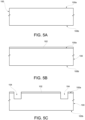
Figure 5A , awafer 100 of semiconductor material, such as for example silicon, is arranged. Thewafer 100 has afront side 100a and arear side 100b, opposite to each other along the Z axis. Thewafer 100 has, for example, a thickness, along the Z axis, equal to about 400 um between thefront side 100a and therear side 100b. - Then,
Figure 5B , a step of forming anetch stop layer 102 on thefront side 100a is performed. Theetch stop layer 102 is of a material that is selectively etchable with respect to the material of the wafer 100 (for example of deposited or thermally grown Silicon Oxide, or TEOS) and has a thickness comprised between about 0.3 um and about 0.7 µm (e.g., equal to 0.5 pm). - Then,
Figure 5C , selective portions of the wafer 100 (including a portion of thelayer 102 and an underlying portion of the wafer 100) are removed using per se known lithography techniques, thus forming alateral groove 104 surrounding a protruding portion 106 having, in top-view, shape and dimensions equal to those of themembrane 40 to be formed. Thegroove 104 ends inside thewafer 100. By way of example, thegroove 104 has, in thewafer 100, a depth (along a direction parallel to the Z axis) of about 5 um and a width (along the X axis) equal to about 5 um. - Then,
Figure 5D , theetch stop layer 102 is restored inside thegroove 104, for example by thermal growth of Silicon Oxide (or other material according to what has already been described with reference toFigure 5B ). - Then,
Figure 5E , a step of forming astructural layer 110 above thefront side 100a, in particular above theetch stop layer 102, is performed. Thestructural layer 110 is, in one embodiment, of the same material as thewafer 100, here of Silicon. Thestructural layer 110 may be formed by Silicon epitaxial growth. Thestructural layer 110 has a thickness for example comprised between 3 um and 100 um; in particular equal to 10 um. Then, the thickness of thestructural layer 110 is reduced by a CMP (Chemical-Mechanical-Planarization) step, up to reaching a final thickness of thestructural layer 110 comprised between 3 µm and 20 µm, in particular equal to 4 um. - Then,
Figure 5F , an insulating or dielectric layer 112 (which, hereinafter will become thelayer 58 ofFigure 1A ,1B ), for example of Silicon Oxide, having a thickness between 0.5 um and 3 µm, in particular equal to 1 µm, is formed on thestructural layer 110. - A step of forming the
actuator 56 and the stiffening structure is then performed. - In one embodiment (exemplified in
Figure 6 ), theactuator 56 is of the piezoelectric type and, in a per se known manner, is formed by astack 60 comprising: afirst electrode 62 of electrically conductor material, for example of titanium (Ti) or platinum (Pt); apiezoelectric material layer 64, for example PZT (Pb, Zr, TiOs) on thefirst electrode 62, in electrical contact therewith; asecond electrode 66, for example of TiW (titanium and tungsten alloy) on thepiezoelectric layer 64, in electrical contact therewith; and adielectric layer 68, for example of silicon oxide and silicon nitride deposited by CVD to protect theelectrodes piezoelectric layer 64. In particular, thedielectric layer 68 extends on the sides of thepiezoelectric material layer 64 and electrically insulates it from theconductive tracks second electrodes 62, 66 (and used to carry the electrical actuation signals of the membrane and/or to receive the transduced signal during the reception step). - As said, the stiffening
structure 113 extends (in sectional view) laterally to thestack 60 and (in top-plan view) surrounds at least partially (completely, in the represented embodiment) theactuator 56 and themembrane 40. - The stiffening
structure 113 is, in one embodiment, formed by thesame stack 60 previously described, in order to optimize the manufacturing steps. - However, it is apparent that the manufacturing process may provide a stiffening structure of other material, a semiconductor and insulating material stack.
- Then,
Figure 5C , the insulatinglayer 112 is patterned so as to remove selective portions of the same which extend between the piezoelectric stack (actuator 56) and thestiffening structure 113 with therespective pillars 36.Trenches 116 are thus formed which extend through the insulatinglayer 112 throughout the entire thickness of the same, up to reaching the underlyingstructural layer 110. Thelayer 58 ofFigure 1A ,1B is thus formed. - The
conductive tracks - Then,
Figure 5H , thepillars 36 are formed above the stiffeningstructure 113 and the respectiveconductive tracks pillars 36 comprises depositing a metal material layer, for example gold, and performing lithography and etching steps of the metal layer using an etching mask patterned so as to define the section designed for the pillars 36 (e.g., one of the sections previously described and illustrated inFigures 2A-2D ). - Alternatively to what has been represented in Figure and described, the
conductive tracks pillars 36, in lateral electrical contact with thepillars 36, and not therebelow. In this case, theconductive tracks - Then,
Figure 5I , thewafer 100 is thinned at therear side 100b, up to reaching a thickness equal to about 100 um. - Subsequently, as shown in
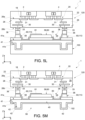
Figure 5L , the wafer 100 (as processed up to the step ofFigure 5I ) is physically and electrically coupled to anASIC assembly 120 through thepillars 36; theASIC assembly 120 includes theredistribution structure 26 and the first and thesecond dice bumps ASIC assembly 120 is then arranged overlapped, along the Z axis, on the wafer 100 (in particular above thefront side 100a). The steps of manufacturing and mutually coupling theredistribution structure 26 and thedice ASIC assembly 120 may be purchased already manufactured, and coupled to thepillars 36 by soldering or bonding techniques known per se. - Without any loss of generality, the manufacture of the
ASIC assembly 120 may occur by so-called FOWLP- ("fan out wafer level package") type processing techniques. In this regard, the first and thesecond dice redistribution structure 26, so as to form indeed theASIC assembly 120. In practice, theASIC assembly 120 is formed by an assembly of dice fixed to each other, after having been previously singulated, in such a way that this assembly has, as a first approximation, the shape of a wafer (in particular, of the wafer 100), in the sense that it may be superimposed on and coupled to thewafer 100, as described. In other words, theASIC assembly 120 represents a kind of "reconstructed wafer". Furthermore, the dice of theASIC assembly 120 share asingle redistribution structure 26. - Then,
Figure 5M , thewafer 100 is etched at therear side 100b, to completely remove the material of thewafer 100 up to reaching theetch stop layer 102. Thethick portions 42 and themembrane portions 40 are thus formed, separated from each other by therecesses 52. The solid body also comprises, in this example, theetch stop layer 102. However, it is apparent that theetch stop layer 102 may be removed by wet etching, if useful or necessary. - Dicing (singulation) steps may then be performed, in a manner not illustrated. In particular, the scribe lines extend laterally to the
pillars 36, i.e. in a zone of thewafer 100 which does not havemembranes 40, noractuators 56, norpillars 36, and is also external to the overlapping region (along the Z axis) between thewafer 100 and theASIC assembly 120. - The advantages that the present manufacturing process affords are clear from the previous description.
- In particular, the device of the present invention is capable of reaching, during use, high vibration frequencies (about 10 MHz) without compromising the performances.
- Finally, it is clear that modifications and variations may be made to the manufacturing process described and illustrated herein, without thereby departing from the scope of the present invention, as defined in the attached claims.
- For example, each electroacoustic device may comprise a different number of dice from what has been shown, in which case the manufacturing process modifies accordingly. The transmission and reception circuits may be formed in different dice; in this case, the transmission and reception circuits may be formed by using different technologies.
- In general, the actuators may be of a different type with respect to what has been described. For example, the actuators may implement an electrostatic, rather than a piezoelectric, actuation mechanism. Similarly, also the arrangement of the actuators with respect to the corresponding membranes may be different from what has been described.
- Furthermore, in lieu of the
bumps - Furthermore, each
pillar 36 may be, in general, a hypocycloid with a number of cusps equal to or greater than three (e.g., five). - Furthermore, the shape of each
pillar 36 may be different forpillars 36 which are different from each other.
Claims (20)
- A MEMS device (1) comprising:- a signal processing assembly (120);- a transduction module (38) comprising a plurality of transducer devices (56) mutually arranged to form an arrangement pattern of transducer devices (56) adjacent to each other and separated from each other by surface regions of the transduction module (38);- a stiffening structure (113) at said surface regions of the transduction module, at least partially surrounding each transducer device (56) of said plurality of transducer devices (56);- a plurality of conductive coupling elements (36) extending on the stiffening structure (113) and configured to physically and electrically couple the transduction module (38) to the signal processing assembly (120), each conductive coupling element (36) being physically separated and electrically insulated from the other conductive coupling elements (36);- a plurality of first conductive tracks (81; 83), each of them electrically connected to a transducer device (56) and to a respective conductive coupling element (36),characterized in that said conductive coupling elements have a respective section with a shape such as to maximize the overlapping surface with the stiffening structure (113) about the respective transducer device (56).
- The device according to claim 1, wherein said conductive coupling elements (36) have a section with a shape of: hypocycloid, with a number of cusps equal to or greater than three; triangular; quadrangular.
- The device according to claim 1 or 2, wherein said arrangement pattern is of matrix or honeycomb type.
- The device according to claim 3, wherein:when said arrangement pattern is of matrix type, the matrix includes rows and columns, each transducer device (56) being arranged at the intersection of a respective row and a respective column of said matrix, and wherein each transducer device (56) is surrounded by four conductive coupling elements (36);when said arrangement pattern is of honeycomb type, each transducer device (56) is surrounded by six conductive coupling elements (36).
- The device according to any of the preceding claims, wherein each transducer device (56) includes a respective membrane (40) and a respective transducer element integral with said respective membrane (40),
wherein each transducer element is electrically controllable by the signal processing assembly (120) to cause a deformation of the corresponding membrane (40). - The device according to claim 5, wherein each transducer element (56) comprises a multilayer, or stack, (60) including:- a bottom electrode (62), of conductive material;- a piezoelectric layer (64) on, and in electrical contact with, the bottom electrode; and- a top electrode (66), on the piezoelectric layer and in electrical contact with the piezoelectric layer,wherein a respective first conductive track (81) between said plurality of first conductive tracks, is in electrical contact with the top electrode (66) and with a respective conductive coupling element (36).
- The device according to claim 6, wherein said bottom electrode (62) is an electrode shared between said plurality of transducer elements (56),
further comprising a second conductive track further with respect to said plurality of first conductive tracks (81; 83), the second conductive track being coupled to said bottom electrode (62) and to a conductive coupling element (36) further with respect to said plurality of conductive coupling elements (36). - The device according to claim 6 or 7, wherein said multilayer (60) further comprises an insulating layer (68) on the top electrode (66),
and wherein the stiffening structure (113) comprises said multilayer (60). - The device according to claim 6, further comprising a plurality of second conductive tracks (83; 81), each of said second conductive tracks being electrically coupled to a respective bottom electrode (62) and to a respective conductive coupling element (36).
- The device according to claim 1, wherein the stiffening structure (113) completely surrounds each transducer device (56), and wherein each conductive coupling element (36) completely surrounds a respective transducer device (56).
- The device according to claim 1, wherein the conductive coupling elements (36) are equal in number to two,and wherein, for each transducer device (56), one of the two conductive coupling elements (36) has a section having a shape of: hypocycloid, with a number of cusps equal to or greater than three; triangular; quadrangular,and wherein the other of the two conductive coupling elements (36) has a section such as to maximize the overlapping surface with the stiffening structure (113) around the respective transducer device (56), where the stiffening structure is free from said one conductive coupling element (36).
- The device according to any of the preceding claims, wherein the conductive coupling elements (36) have an elongated shape with an extension direction along an axis (Z), said section being taken on a plane (XY) orthogonal to said axis (Z).
- The device according to any of the preceding claims, wherein the stiffening structure (113) is a multilayer having a thickness comprised between 1 um and 50 µm.
- The device according to any of the preceding claims, wherein the signal processing assembly (120) comprises a redistribution structure (26) provided with a first side (26a) and a second side (26b) opposite to each other, and with redistribution conductive paths (30) which extend between the first side and the second side,
wherein the redistribution structure (26) faces the transduction module (38) by the second side (26b) and is provided, at the second side, with connection pads (33) electrically coupled between respective conductive paths (30) and respective conductive coupling elements (36). - The device according to claim 14, wherein the signal processing assembly (120) further comprises a control module (2, 4, 22),said redistribution structure (26) being provided, at the first side, with further connection pads (31) electrically coupled to respective conductive paths (30),the control module (2, 4, 22) being arranged facing the first side (26a) of the redistribution structure (26) and being electrically coupled to said further connection pads (31) .
- The device according to claim 15, wherein the conductive coupling elements (36), the connection pads (33), the redistribution conductive paths (30), and the further connection pads (31) form a plurality of conductive paths configured to carry electrical signals between the control module (2, 4, 22) and the transduction module (38).
- The device according to any of the preceding claims, wherein said MEMS device (1) is an ultrasound transducer device, or PMUT.
- A method of manufacturing a MEMS device, comprising the steps of:- forming a transduction module (38), comprising forming a plurality of transducer devices (56) mutually arranged according to an arrangement pattern of transducer devices (56) adjacent to each other and separated from each other by surface regions of the transduction module (38);- forming a stiffening structure (113) at said surface regions of the transduction module, at least partially surrounding each transducer device (56) of said plurality of transducer devices (56);- forming a plurality of conductive coupling elements (36) on the stiffening structure (113), each conductive coupling element (36) being configured to physically and electrically couple the transduction module (38) to the signal processing assembly (120), and being physically separated and electrically insulated from the other conductive coupling elements (36);- forming a plurality of first conductive tracks (81; 83), each of them electrically connected to a transducer device (56) and to a respective conductive coupling element (36) ;- coupling a signal processing assembly (120) to said plurality of conductive coupling elements (36),characterized in that said conductive coupling elements (36) have a section with a shape such as to maximize the overlapping surface with the stiffening structure (113) around the respective transducer device (56).
- The method according to claim 18, wherein forming each transducer device (56) includes forming a respective membrane (40) and a respective transducer element integral with said respective membrane (40),
and wherein forming each respective membrane includes:- forming, in a semiconductor body (100), an etch stop layer (102);- forming, on the etch stop layer, a structural layer (110) ;- forming, on the structural layer, an insulation layer (112);- forming, on the insulation layer, said respective transducer element (56) and said first connection pads associated with said respective transducer element (56), the first connection pads being arranged laterally to the respective transducer element (56);- removing selective portions of the insulation layer which extend between the transducer element (56) and the first connection pads; and- completely removing the semiconductor body (100) exposing the etch stop layer (102). - The method according to claim 19, further comprising the step of forming supports (42) for each membrane (40), including the steps of:- forming a respective trench (104) in the semiconductor body, said trench externally delimiting the shape of the respective membrane (40) and having a closed circular or polygonal shape;- forming the etch stop layer (102) on the semiconductor body and in said trench (104); and- forming the structural layer (110) on the etch stop layer (102) which extends both on the semiconductor body and in said trench.
Applications Claiming Priority (1)
| Application Number | Priority Date | Filing Date | Title |
|---|---|---|---|
| IT102022000024411A IT202200024411A1 (en) | 2022-11-25 | 2022-11-25 | MEMS TRANSDUCER DEVICE FOR HIGH FREQUENCY APPLICATIONS, AND MANUFACTURING METHOD |
Publications (2)
| Publication Number | Publication Date |
|---|---|
| EP4378883A1 true EP4378883A1 (en) | 2024-06-05 |
| EP4378883B1 EP4378883B1 (en) | 2025-12-24 |
Family
ID=85128709
Family Applications (1)
| Application Number | Title | Priority Date | Filing Date |
|---|---|---|---|
| EP23207483.1A Active EP4378883B1 (en) | 2022-11-25 | 2023-11-02 | Mems transducer device for high-frequency applications, and manufacturing method |
Country Status (3)
| Country | Link |
|---|---|
| US (1) | US12610197B2 (en) |
| EP (1) | EP4378883B1 (en) |
| IT (1) | IT202200024411A1 (en) |
Citations (1)
| Publication number | Priority date | Publication date | Assignee | Title |
|---|---|---|---|---|
| EP3599217A1 (en) | 2018-07-23 | 2020-01-29 | STMicroelectronics S.r.l. | A process for manufacturing microelectromechanical devices, in particular electroacoustic modules |
Family Cites Families (9)
| Publication number | Priority date | Publication date | Assignee | Title |
|---|---|---|---|---|
| DE102011084393A1 (en) * | 2011-10-13 | 2013-04-18 | Robert Bosch Gmbh | Micromechanical functional device, in particular speaker device, and corresponding manufacturing method |
| KR102155695B1 (en) * | 2014-02-12 | 2020-09-21 | 삼성전자주식회사 | Electro acoustic transducer |
| US9344808B2 (en) * | 2014-03-18 | 2016-05-17 | Invensense, Inc. | Differential sensing acoustic sensor |
| CN104796832B (en) * | 2015-02-16 | 2018-10-16 | 迈尔森电子(天津)有限公司 | MEMS microphone and forming method thereof |
| IT201700082961A1 (en) | 2017-07-20 | 2019-01-20 | St Microelectronics Srl | MICROFLUID MEMS DEVICE FOR THE PRINTING OF JET INKS WITH PIEZOELECTRIC IMPLEMENTATION AND ITS MANUFACTURING METHOD |
| US10966683B2 (en) * | 2018-03-22 | 2021-04-06 | Exo Imaging Inc. | Integrated ultrasonic transducers |
| US11502067B2 (en) * | 2018-07-26 | 2022-11-15 | Advanced Semiconductor Engineering, Inc. | Package structure and method for manufacturing the same |
| US10785576B1 (en) * | 2019-04-30 | 2020-09-22 | Sae Magnetics (H.K.) Ltd. | MEMS package, MEMS microphone, method of manufacturing the MEMS package and method of manufacturing the MEMS microphone |
| US12284480B2 (en) | 2022-12-14 | 2025-04-22 | Stmicroelectronics International N.V. | Transducer assembly with buried cavities and method of manufacturing the same |
-
2022
- 2022-11-25 IT IT102022000024411A patent/IT202200024411A1/en unknown
-
2023
- 2023-11-02 EP EP23207483.1A patent/EP4378883B1/en active Active
- 2023-11-17 US US18/513,248 patent/US12610197B2/en active Active
Patent Citations (1)
| Publication number | Priority date | Publication date | Assignee | Title |
|---|---|---|---|---|
| EP3599217A1 (en) | 2018-07-23 | 2020-01-29 | STMicroelectronics S.r.l. | A process for manufacturing microelectromechanical devices, in particular electroacoustic modules |
Also Published As
| Publication number | Publication date |
|---|---|
| US20240179475A1 (en) | 2024-05-30 |
| US12610197B2 (en) | 2026-04-21 |
| EP4378883B1 (en) | 2025-12-24 |
| IT202200024411A1 (en) | 2024-05-25 |
Similar Documents
| Publication | Publication Date | Title |
|---|---|---|
| US8466522B2 (en) | Element array, electromechanical conversion device, and process for producing the same | |
| US11839159B2 (en) | Transducer with improved piezoelectric arrangement, mems device comprising the transducer, and methods for manufacturing the transducer | |
| US7053456B2 (en) | Electronic component having micro-electrical mechanical system | |
| JP4981223B2 (en) | Microfabricated transducer formed on other circuit components on integrated circuit chip and method of manufacturing the same | |
| JP5754145B2 (en) | Ultrasonic sensors and electronics | |
| US20080315331A1 (en) | Ultrasound system with through via interconnect structure | |
| JP5851238B6 (en) | Ultrasonic transducer, its manufacturing method, and ultrasonic probe using the same | |
| JP2018046512A (en) | Piezoelectric device and ultrasound apparatus | |
| EP3599217B1 (en) | A process for manufacturing microelectromechanical devices, in particular electroacoustic modules | |
| JP4724501B2 (en) | Ultrasonic transducer and manufacturing method thereof | |
| CN106744642A (en) | The hybrid ultrasonic transducer face battle array probe of broadband and preparation method of receiving-transmitting balance | |
| CN116507580B (en) | Micromechanical components, acoustic transducer devices, and methods for manufacturing micromechanical components | |
| US20180221917A1 (en) | Capacitive micromachined ultrasonic transducer and method for manufacturing the same | |
| US20240327203A1 (en) | Method for manufacturing a mems transducer device with thin membrane, and mems transducer device | |
| JP6606034B2 (en) | Capacitive detection type ultrasonic transducer and ultrasonic imaging apparatus including the same | |
| EP4378883B1 (en) | Mems transducer device for high-frequency applications, and manufacturing method | |
| JP6090365B2 (en) | Ultrasonic sensors and electronics | |
| TW202213824A (en) | Piezoelectric micromachined ultrasonic transducer and method of fabricating the same | |
| CN118083901A (en) | MEMS transducer device for high frequency applications and method of manufacture | |
| US12172187B2 (en) | Ultrasound transducer manufacturing method | |
| EP3905716B1 (en) | Ultrasound device |
Legal Events
| Date | Code | Title | Description |
|---|---|---|---|
| PUAI | Public reference made under article 153(3) epc to a published international application that has entered the european phase |
Free format text: ORIGINAL CODE: 0009012 |
|
| STAA | Information on the status of an ep patent application or granted ep patent |
Free format text: STATUS: THE APPLICATION HAS BEEN PUBLISHED |
|
| AK | Designated contracting states |
Kind code of ref document: A1 Designated state(s): AL AT BE BG CH CY CZ DE DK EE ES FI FR GB GR HR HU IE IS IT LI LT LU LV MC ME MK MT NL NO PL PT RO RS SE SI SK SM TR |
|
| STAA | Information on the status of an ep patent application or granted ep patent |
Free format text: STATUS: REQUEST FOR EXAMINATION WAS MADE |
|
| 17P | Request for examination filed |
Effective date: 20241127 |
|
| RBV | Designated contracting states (corrected) |
Designated state(s): AL AT BE BG CH CY CZ DE DK EE ES FI FR GB GR HR HU IE IS IT LI LT LU LV MC ME MK MT NL NO PL PT RO RS SE SI SK SM TR |
|
| GRAP | Despatch of communication of intention to grant a patent |
Free format text: ORIGINAL CODE: EPIDOSNIGR1 |
|
| STAA | Information on the status of an ep patent application or granted ep patent |
Free format text: STATUS: GRANT OF PATENT IS INTENDED |
|
| RIC1 | Information provided on ipc code assigned before grant |
Ipc: B81C 1/00 20060101AFI20250521BHEP |
|
| INTG | Intention to grant announced |
Effective date: 20250613 |
|
| GRAS | Grant fee paid |
Free format text: ORIGINAL CODE: EPIDOSNIGR3 |
|
| GRAA | (expected) grant |
Free format text: ORIGINAL CODE: 0009210 |
|
| STAA | Information on the status of an ep patent application or granted ep patent |
Free format text: STATUS: THE PATENT HAS BEEN GRANTED |
|
| AK | Designated contracting states |
Kind code of ref document: B1 Designated state(s): AL AT BE BG CH CY CZ DE DK EE ES FI FR GB GR HR HU IE IS IT LI LT LU LV MC ME MK MT NL NO PL PT RO RS SE SI SK SM TR |
|
| REG | Reference to a national code |
Ref country code: CH Ref legal event code: F10 Free format text: ST27 STATUS EVENT CODE: U-0-0-F10-F00 (AS PROVIDED BY THE NATIONAL OFFICE) Effective date: 20251224 Ref country code: GB Ref legal event code: FG4D |
|
| REG | Reference to a national code |
Ref country code: DE Ref legal event code: R096 Ref document number: 602023010049 Country of ref document: DE |
|
| REG | Reference to a national code |
Ref country code: LT Ref legal event code: MG9D |
|
| PG25 | Lapsed in a contracting state [announced via postgrant information from national office to epo] |
Ref country code: NO Free format text: LAPSE BECAUSE OF FAILURE TO SUBMIT A TRANSLATION OF THE DESCRIPTION OR TO PAY THE FEE WITHIN THE PRESCRIBED TIME-LIMIT Effective date: 20260324 |
|
| PG25 | Lapsed in a contracting state [announced via postgrant information from national office to epo] |
Ref country code: FI Free format text: LAPSE BECAUSE OF FAILURE TO SUBMIT A TRANSLATION OF THE DESCRIPTION OR TO PAY THE FEE WITHIN THE PRESCRIBED TIME-LIMIT Effective date: 20251224 Ref country code: HR Free format text: LAPSE BECAUSE OF FAILURE TO SUBMIT A TRANSLATION OF THE DESCRIPTION OR TO PAY THE FEE WITHIN THE PRESCRIBED TIME-LIMIT Effective date: 20251224 |
|
| PG25 | Lapsed in a contracting state [announced via postgrant information from national office to epo] |
Ref country code: RS Free format text: LAPSE BECAUSE OF FAILURE TO SUBMIT A TRANSLATION OF THE DESCRIPTION OR TO PAY THE FEE WITHIN THE PRESCRIBED TIME-LIMIT Effective date: 20260324 |
|
| PG25 | Lapsed in a contracting state [announced via postgrant information from national office to epo] |
Ref country code: LV Free format text: LAPSE BECAUSE OF FAILURE TO SUBMIT A TRANSLATION OF THE DESCRIPTION OR TO PAY THE FEE WITHIN THE PRESCRIBED TIME-LIMIT Effective date: 20251224 |
|
| REG | Reference to a national code |
Ref country code: NL Ref legal event code: MP Effective date: 20251224 |
|
| PG25 | Lapsed in a contracting state [announced via postgrant information from national office to epo] |
Ref country code: BG Free format text: LAPSE BECAUSE OF FAILURE TO SUBMIT A TRANSLATION OF THE DESCRIPTION OR TO PAY THE FEE WITHIN THE PRESCRIBED TIME-LIMIT Effective date: 20251224 |