EP4376224A1 - Connector assembly - Google Patents
Connector assembly Download PDFInfo
- Publication number
- EP4376224A1 EP4376224A1 EP23201603.0A EP23201603A EP4376224A1 EP 4376224 A1 EP4376224 A1 EP 4376224A1 EP 23201603 A EP23201603 A EP 23201603A EP 4376224 A1 EP4376224 A1 EP 4376224A1
- Authority
- EP
- European Patent Office
- Prior art keywords
- connector
- contact
- contacts
- insulator
- contacting
- Prior art date
- Legal status (The legal status is an assumption and is not a legal conclusion. Google has not performed a legal analysis and makes no representation as to the accuracy of the status listed.)
- Granted
Links
Images








Classifications
-
- H—ELECTRICITY
- H01—ELECTRIC ELEMENTS
- H01R—ELECTRICALLY-CONDUCTIVE CONNECTIONS; STRUCTURAL ASSOCIATIONS OF A PLURALITY OF MUTUALLY-INSULATED ELECTRICAL CONNECTING ELEMENTS; COUPLING DEVICES; CURRENT COLLECTORS
- H01R13/00—Details of coupling devices of the kinds covered by groups H01R12/70 or H01R24/00 - H01R33/00
- H01R13/40—Securing contact members in or to a base or case; Insulating of contact members
- H01R13/42—Securing in a demountable manner
- H01R13/422—Securing in resilient one-piece base or case, e.g. by friction; One-piece base or case formed with resilient locking means
-
- H—ELECTRICITY
- H01—ELECTRIC ELEMENTS
- H01R—ELECTRICALLY-CONDUCTIVE CONNECTIONS; STRUCTURAL ASSOCIATIONS OF A PLURALITY OF MUTUALLY-INSULATED ELECTRICAL CONNECTING ELEMENTS; COUPLING DEVICES; CURRENT COLLECTORS
- H01R12/00—Structural associations of a plurality of mutually-insulated electrical connecting elements, specially adapted for printed circuits, e.g. printed circuit boards [PCB], flat or ribbon cables, or like generally planar structures, e.g. terminal strips, terminal blocks; Coupling devices specially adapted for printed circuits, flat or ribbon cables, or like generally planar structures; Terminals specially adapted for contact with, or insertion into, printed circuits, flat or ribbon cables, or like generally planar structures
- H01R12/50—Fixed connections
- H01R12/59—Fixed connections for flexible printed circuits, flat or ribbon cables or like structures
- H01R12/592—Fixed connections for flexible printed circuits, flat or ribbon cables or like structures connections to contact elements
-
- H—ELECTRICITY
- H01—ELECTRIC ELEMENTS
- H01R—ELECTRICALLY-CONDUCTIVE CONNECTIONS; STRUCTURAL ASSOCIATIONS OF A PLURALITY OF MUTUALLY-INSULATED ELECTRICAL CONNECTING ELEMENTS; COUPLING DEVICES; CURRENT COLLECTORS
- H01R13/00—Details of coupling devices of the kinds covered by groups H01R12/70 or H01R24/00 - H01R33/00
- H01R13/62—Means for facilitating engagement or disengagement of coupling parts or for holding them in engagement
- H01R13/639—Additional means for holding or locking coupling parts together, after engagement, e.g. separate keylock, retainer strap
-
- H—ELECTRICITY
- H01—ELECTRIC ELEMENTS
- H01R—ELECTRICALLY-CONDUCTIVE CONNECTIONS; STRUCTURAL ASSOCIATIONS OF A PLURALITY OF MUTUALLY-INSULATED ELECTRICAL CONNECTING ELEMENTS; COUPLING DEVICES; CURRENT COLLECTORS
- H01R12/00—Structural associations of a plurality of mutually-insulated electrical connecting elements, specially adapted for printed circuits, e.g. printed circuit boards [PCB], flat or ribbon cables, or like generally planar structures, e.g. terminal strips, terminal blocks; Coupling devices specially adapted for printed circuits, flat or ribbon cables, or like generally planar structures; Terminals specially adapted for contact with, or insertion into, printed circuits, flat or ribbon cables, or like generally planar structures
- H01R12/50—Fixed connections
- H01R12/59—Fixed connections for flexible printed circuits, flat or ribbon cables or like structures
- H01R12/61—Fixed connections for flexible printed circuits, flat or ribbon cables or like structures connecting to flexible printed circuits, flat or ribbon cables or like structures
-
- H—ELECTRICITY
- H01—ELECTRIC ELEMENTS
- H01R—ELECTRICALLY-CONDUCTIVE CONNECTIONS; STRUCTURAL ASSOCIATIONS OF A PLURALITY OF MUTUALLY-INSULATED ELECTRICAL CONNECTING ELEMENTS; COUPLING DEVICES; CURRENT COLLECTORS
- H01R12/00—Structural associations of a plurality of mutually-insulated electrical connecting elements, specially adapted for printed circuits, e.g. printed circuit boards [PCB], flat or ribbon cables, or like generally planar structures, e.g. terminal strips, terminal blocks; Coupling devices specially adapted for printed circuits, flat or ribbon cables, or like generally planar structures; Terminals specially adapted for contact with, or insertion into, printed circuits, flat or ribbon cables, or like generally planar structures
- H01R12/50—Fixed connections
- H01R12/59—Fixed connections for flexible printed circuits, flat or ribbon cables or like structures
- H01R12/65—Fixed connections for flexible printed circuits, flat or ribbon cables or like structures characterised by the terminal
-
- H—ELECTRICITY
- H01—ELECTRIC ELEMENTS
- H01R—ELECTRICALLY-CONDUCTIVE CONNECTIONS; STRUCTURAL ASSOCIATIONS OF A PLURALITY OF MUTUALLY-INSULATED ELECTRICAL CONNECTING ELEMENTS; COUPLING DEVICES; CURRENT COLLECTORS
- H01R13/00—Details of coupling devices of the kinds covered by groups H01R12/70 or H01R24/00 - H01R33/00
- H01R13/46—Bases; Cases
- H01R13/502—Bases; Cases composed of different pieces
- H01R13/506—Bases; Cases composed of different pieces assembled by snap action of the parts
-
- H—ELECTRICITY
- H01—ELECTRIC ELEMENTS
- H01R—ELECTRICALLY-CONDUCTIVE CONNECTIONS; STRUCTURAL ASSOCIATIONS OF A PLURALITY OF MUTUALLY-INSULATED ELECTRICAL CONNECTING ELEMENTS; COUPLING DEVICES; CURRENT COLLECTORS
- H01R13/00—Details of coupling devices of the kinds covered by groups H01R12/70 or H01R24/00 - H01R33/00
- H01R13/62—Means for facilitating engagement or disengagement of coupling parts or for holding them in engagement
- H01R13/629—Additional means for facilitating engagement or disengagement of coupling parts, e.g. aligning or guiding means, levers, gas pressure electrical locking indicators, manufacturing tolerances
- H01R13/631—Additional means for facilitating engagement or disengagement of coupling parts, e.g. aligning or guiding means, levers, gas pressure electrical locking indicators, manufacturing tolerances for engagement only
-
- H—ELECTRICITY
- H01—ELECTRIC ELEMENTS
- H01R—ELECTRICALLY-CONDUCTIVE CONNECTIONS; STRUCTURAL ASSOCIATIONS OF A PLURALITY OF MUTUALLY-INSULATED ELECTRICAL CONNECTING ELEMENTS; COUPLING DEVICES; CURRENT COLLECTORS
- H01R24/00—Two-part coupling devices, or either of their cooperating parts, characterised by their overall structure
Definitions
- the present invention relates to a connector assembly, particularly to a connector assembly used to fit a module-side connector of a wearable device to a garment-side connector to establish electrical connection therebetween.
- smart clothes that can obtain user's biological data such as the heart rate and the body temperature only by being worn by the user.
- Such smart clothes have an electrode disposed at a measurement site, and when a wearable device serving as a measurement device is electrically connected to the electrode, biological data can be transmitted to the wearable device.
- the electrode and the wearable device can be interconnected by, for instance, use of a connector connected to a conductor drawn from the electrode.
- JP 2019-87515 A discloses a connector as illustrated in FIG. 74 .
- the connector includes a garment-side connector portion 1 to be attached to a garment and a module-side connector portion 2 to be fitted to the garment-side connector portion 1.
- the garment-side connector portion 1 includes a module-side connector accommodating portion 3 of recess shape and a plurality of garment-side contacts 4 aligned within the module-side connector accommodating portion 3, and the garment-side contacts 4 are connected to conductor portions of a conductive sheet 5 disposed on the garment.
- the module-side connector portion 2 includes a plurality of module-side contacts 6 aligned to correspond to the garment-side contacts 4.
- the module-side connector portion 2 When the module-side connector portion 2 is accommodated into the module-side connector accommodating portion 3 of the garment-side connector portion 1, the module-side connector portion 2 is fitted to the garment-side connector portion 1, and the module-side contacts 6 are connected to the garment-side contacts 4.
- this configuration requires formation of the locking portion 7 in the garment-side connector portion 1 and the to-be-locked portion 8 in the module-side connector portion 2 to prevent the module-side connector portion 2 from coming off the module-side connector accommodating portion 3 of the garment-side connector portion 1 and retain the fitting state between the garment-side connector portion 1 and the module-side connector portion 2, resulting in a complex structure of the connector.
- the present invention has been made to overcome such a conventional problem and provide a connector assembly that can stably maintain a fitting state even with a simple structure.
- a connector assembly according to the present invention is one including a first connector and a second connector that are fitted to each other along a fitting direction such that a second contact of the second connector is electrically connected to a first contact of the first connector,
- FIG. 1 shows a connector assembly according to Embodiment 1 before fitting.
- the connector assembly is composed of a first connector 11 and a second connector 21 to be fitted to each other.
- the first connector 11 is used as a garment-side connector to be attached to a garment
- the second connector 21 is used as a module-side connector to be fitted to the first connector 11.
- the first connector 11 includes: a first insulator 12 made of an insulating material; and a plurality of first contacts 13 aligned in a predetermined direction and held by the first insulator 12.
- the first insulator 12 is attached to a tab sheet 14.
- the second connector 21 includes: a second insulator 22 made of an insulating material; and a plurality of second contacts 23 aligned in a predetermined direction in the same manner as the plurality of first contacts 13 of the first connector 11 and held by the second insulator 22.
- the plurality of first contacts 13 and the plurality of second contacts 23 are aligned in parallel to each other at the same alignment pitch.
- a direction in which the plurality of first contacts 13 and the plurality of second contacts 23 are aligned is defined as "Y direction,” a direction from the first connector 11 to the second connector 21 as “+Z direction,” and a direction perpendicular to the Y direction and the Z direction as “X direction.”
- the Z direction is a fitting direction in which the second connector 21 is fitted to the first connector 11.
- FIG. 2 is an exploded perspective view of the first connector 11.
- the first connector 11 includes a bottom insulator 15 and a top insulator 16, and these bottom and top insulators 15 and 16 constitute the first insulator 12.
- the plurality of first contacts 13 are disposed on the +Z direction side from the bottom insulator 15, and a circuit board 17 is disposed on the +Z direction side from the plurality of first contacts 13. Further, the tab sheet 14 is disposed on the +Z direction side from the circuit board 17, and the top insulator 16 is disposed on the +Z direction side from the tab sheet 14.
- the tab sheet 14 is made of, for instance, cloth of a garment to which the first connector 11 is to be attached as the garment-side connector, and the tab sheet 14 has a rectangular opening 14A.
- the bottom insulator 15 includes a flat plate portion 15A extending along an XY plane, and a plurality of contact supporting portions 15B of protrusion shape are formed to be aligned in the Y direction on the top surface, facing the +Z direction, of the flat plate portion 15A.
- a plurality of projections 15C are formed to be aligned in the Y direction on the top surface, facing the +Z direction, of the flat plate portion 15A on the -X direction side from the plurality of contact supporting portions 15B.
- a plurality of contact insertion portions 15D are each formed by a gap between adjacent projections 15C.
- the plurality of contact insertion portions 15D are situated at the same Y-directional positions as the plurality of contact supporting portions 15B, and the plurality of contact supporting portions 15B and the plurality of contact insertion portions 15D correspond to the plurality of first contacts 13.
- the flat plate portion 15A is provided at its +X directional end with a tab sheet supporting portion 15E extending in the Y direction and protruding in the +Z direction.
- the first contact 13 is formed from a band-shaped plate member that is made of a conductive material such as metal and that is bent, and the first contact 13 includes a retention projection 13A bent in a U shape and extending in the Z direction.
- the retention projection 13A has a lateral surface 13B facing the -X direction and a lateral surface 13C facing the +X direction, and the lateral surface 13B is provided at its +Z directional end with a hook portion 13D protruding in a right angle shape or a chevron shape and facing the -X direction and the -Z direction.
- the lateral surface 13C is provided with a protrusion portion 13E protruding in the +X direction on the -Z direction side from the hook portion 13D at a position closer to the base portion of the retention projection 13A than the hook portion 13D is.
- the -Z directional end of the lateral surface 13B is provided with a bent portion 13F protruding in the -Z direction.
- a cantilever portion 13G extends in the -X direction from the bent portion 13F.
- the -X directional end of the cantilever portion 13G is provided with a curved portion 13H curving in a convex shape toward the +Z direction.
- the circuit board 17 is constituted of, for example, a so-called flexible printed circuit (FPC), and a plurality of connection portions 17A aligned in the Y direction are exposed on the bottom surface, facing the -Z direction, of the circuit board 17 at the +X directional end of the circuit board 17.
- the plurality of connection portions 17A correspond to the plurality of first contacts 13.
- the top insulator 16 includes a flat plate portion 16A extending along an XY plane, and a plurality of projections 16B aligned in the Y direction and projecting in the +Z direction are formed on the top surface, facing the +Z direction, of the flat plate portion 16A.
- a plurality of through-holes 16C penetrating the flat plate portion 16A in the Z direction as shown in FIG. 7 are each formed between adjacent projections 16B.
- a plurality of protuberance portions 16D aligned in the Y direction and projecting in the +Z direction are formed on the top surface, facing the +Z direction, of the flat plate portion 16A on the -X direction side from the plurality of projections 16B.
- the plurality of protuberance portions 16D are situated at the same Y-directional positions as the plurality of through-holes 16C, and the plurality of through-holes 16C and the plurality of protuberance portions 16D correspond to the plurality of first contacts 13.
- the retention projection 13A of the first contact 13 is inserted into the corresponding through-hole 16C of the top insulator 16 from the -Z direction within the opening 14A of the tab sheet 14, and the tab sheet 14 and the circuit board 17 are sandwiched between the flat plate portion 15A of the bottom insulator 15 and the flat plate portion 16A of the top insulator 16 such that the connection portion 17A of the circuit board 17 is situated on the +Z direction side of the curved portion 13H of the corresponding first contact 13.
- the bottom insulator 15 and the top insulator 16 are fixed to each other.
- the bottom insulator 15 and the top insulator 16 may be fixed to each other by being adhered to the tab sheet 14 and the circuit board 17, or alternatively by another method, e.g., by inserting a boss formed to project on one of the bottom insulator 15 and the top insulator 16 into a through-hole formed in the other thereof and deforming the tip of the boss by heat.
- the first contact 13 is retained by the bottom insulator 15 and the top insulator 16 with the bent portion 13F being situated on the contact supporting portion 15B of the bottom insulator 15, the -X directional end of the cantilever portion 13G being inserted in the contact insertion portion 15D of the bottom insulator 15, and the curved portion 13H being in contact with the connection portion 17A of the circuit board 17.
- first contact 13 does not have a fixation portion fixed to the bottom insulator 15 and the top insulator 16, a part of the first contact 13 may be fixed to one of the bottom insulator 15 and the top insulator 16.
- the top surface, facing the +Z direction, of the flat plate portion 16A of the top insulator 16 forms a first exposed surface S1 facing the second connector 21, and the retention projection 13A of the first contact 13 projects in the +Z direction from the first exposed surface S1.
- a first contacting portion P1 facing the -X direction and the -Z direction is set by the hook portion 13D of the first contact 13
- a second contacting portion P2 facing the +X direction and situated on the -Z direction side from the first contacting portion P1 is set by the protrusion portion 13E of the first contact 13
- a third contacting portion P3 situated on the first exposed surface S1 at a position away from the first contacting portion P1 in the -X direction and facing the +Z direction is set by the protuberance portion 16D of the top insulator 16.
- the second connector 21 is retained with respect to the first connector 11 owing to the first contacting portion P1, the second contacting portion P2, and the third contacting portion P3 making contact with the second connector 21.
- the second insulator 22 has a rectangular cuboid outer shape and includes a plurality of contact accommodating portions 22A of recess shape aligned in the Y direction and each extending in the X direction and the Z direction.
- a partition plate 22B extending along an XZ plane is formed between adjacent contact accommodating portions 22A.
- Each partition plate 22B is provided with a U-shaped cutout 22C opening toward the -Z direction.
- the second contact 23 is formed from a band-shaped plate member that is made of a conductive material such as metal and that is bent, and the second contact 23 includes a U-shaped portion 23A curved in a U shape opening toward the -Z direction.
- the U-shaped portion 23A includes a first extension portion 23B extending along a YZ plane on the -X direction side and a second extension portion 23C extending along a YZ plane on the +X direction side.
- a projection accommodating portion 23D of recess shape is formed inside the U-shaped portion 23A to accommodate the retention projection 13A of the first contact 13.
- the surface, on the +X direction side, of the first extension portion 23B facing the projection accommodating portion 23D is provided with a receiving portion 23E formed by a concavity for receiving the hook portion 13D of the first contact 13.
- the second contact 23 has a bottom portion 23F extending in the -X direction from the -Z directional end of the first extension portion 23B.
- the bottom portion 23F is provided with a step portion 23G that goes down in the -Z direction, and a rising portion 23H is formed to rise in the +Z direction from the -X directional end of the step portion 23G.
- the second contact 23 further has a rising portion 23J bent toward the +X direction from the -Z directional end of the second extension portion 23C and rising in the +Z direction.
- the second contact 23 is accommodated in the contact accommodating portion 22A of the second insulator 22 from the +Z direction.
- the rising portions 23H and 23J of the second contact 23 are respectively pressed against the inner surfaces of the -X and +X directional ends of the contact accommodating portion 22A, so that the second contact 23 is retained in the second insulator 22.
- the contact accommodating portion 22A of the second insulator 22 is provided with a through-hole 22D penetrating in the Z direction.
- the step portion 23G of the second contact 23 is inserted in the through-hole 22D, whereby the bottom surface, facing the -Z direction, of the step portion 23G forms the substantially same plane as the bottom surface, on the -Z direction side, of the second insulator 22, and those bottom surfaces together form a second exposed surface S2 facing the -Z direction.
- the projection accommodating portion 23D formed inside the U-shaped portion 23A of the second contact 23 is situated to overlap the cutout 22C formed in the partition plate 22B of the second insulator 22 as viewed from the Y direction.
- a +Z directional portion of the retention projection 13A of the first contact 13 of the first connector 11 is inserted into the projection accommodating portion 23D of the second contact 23 of the second connector 21 from the -Z direction, the hook portion 13D of the retention projection 13A is received by the receiving portion 23E of the second contact 23, and the protrusion portion 13E of the retention projection 13A makes contact with the inner surface, on the +X direction side, of the projection accommodating portion 23D of the second contact 23.
- the protuberance portion 16D formed on the first exposed surface S1 of the top insulator 16 of the first connector 11 makes contact with the bottom surface of the step portion 23G of the second contact 23 which bottom surface forms the second exposed surface S2 of the second connector 21.
- the second contact 23 of the second connector 21 receives a force F1 acting in the -X direction and the -Z direction from the first contacting portion P1 set at the hook portion 13D of the retention projection 13A of the first contact 13 of the first connector 11, a force F2 acting in the +X direction from the second contacting portion P2 set at the protrusion portion 13E of the retention projection 13A of the first contact 13 of the first connector 11, and a force F3 acting in the +Z direction from the third contacting portion P3 set at the protuberance portion 16D of the top insulator 16 of the first connector 11.
- the inner surface of the projection accommodating portion 23D of the second contact 23 receives the force F1 and the force F2 separately from the first contacting portion P1 and the second contacting portion P2 of the retention projection 13A of the first contact 13, whereby the first contact 13 is electrically connected to the second contact 23.
- the curved portion 13H of the first contact 13 makes contact with the connection portion 17A of the circuit board 17, so that the first contact 13 is electrically connected to the connection portion 17A of the circuit board 17; thus, the second contact 23 is electrically connected to the connection portion 17A of the circuit board 17 via the first contact 13 in the fitting state between the first connector 11 and the second connector 21.
- F 2 ⁇ LZ F 3 ⁇ LX where the distance between the first contacting portion P1 and the third contacting portion P3 in the X direction is LX, and the distance between the first contacting portion P1 and the second contacting portion P2 in the Z direction is LZ.
- the ratio of the component force F1Z of the force F1 in the Z direction to the component force F1X of the force F1 in the X direction (F1Z/F1X) is to be equal to an incline S of the normal line N.
- the second contact 23 is supported at three points by the first contacting portion P1, the second contacting portion P2, and the third contacting portion P3.
- the second connector 21 receives the forces F1 acting in the -X direction and the -Z direction from the first contacting portions P1 of the plurality of first contacts 13 of the first connector 11, the forces F2 acting in the +X direction from the second contacting portions P2 thereof, and the forces F3 acting in the +Z direction from the third contacting portions P3 of the plurality of protuberance portions 16D of the top insulator 16.
- first connector 11 in place of the first connector 11, use is made of, for example, a first connector identical to the first connector 11 except that the protuberance portion 16D on the first exposed surface S1 of the top insulator 16 is positioned off to the -X direction side compared to that of the first connector 11.
- the position of the protuberance portion 16D off to the -X direction side results in a longer distance LX between the first contacting portion P1 and the third contacting portion P3 in the X direction; consequently, based on Formula (3) above, the force F3 in the +Z direction acting from the third contacting portion P3 to the second connector 21 decreases in an attempt to balance the moments about the first contacting portion P1, and the component force F1Z of the force F1 in the Z direction decreases accordingly.
- the component force F1X of the force F1 in the X direction is equal to the force F2 and is unchanged, the ratio (F1Z/F1X) tends to be smaller than the incline S of the normal line N.
- the force F1 along the normal line N acts from the first contacting portion P1 as a normal force from the tangent plane T, and a force acting in the -Z direction corresponding to the decrease of the component force F1Z of the force F1 in the Z direction is to act from the first contacting portion P1 to the second connector 21.
- the second connector 21 is prevented from coming off the first connector in the +Z direction.
- the position of the protuberance portion 16D off to the +X direction side results in a shorter distance LX between the first contacting portion P1 and the third contacting portion P3 in the X direction; consequently, based on Formula (3) above, the force F3 in the +Z direction acting from the third contacting portion P3 to the second connector 21 increases in an attempt to balance the moments about the first contacting portion P1, and the component force F1Z of the force F1 in the Z direction increases accordingly.
- the component force F1X of the force F1 in the X direction is equal to the force F2 and is unchanged, the ratio (F1Z/F1X) tends to be greater than the incline S of the normal line N.
- the force F1 along the normal line N acts from the first contacting portion P1 as a normal force from the tangent plane T, and a force acting in the +Z direction corresponding to the increase of the component force F1Z of the force F1 in the Z direction is to act from the first contacting portion P1 to the second connector 21.
- the second connector 21 easily comes off the first connector in the +Z direction.
- the ratio LZ/LX of the distance LZ between the first contacting portion P1 and the second contacting portion P2 in the Z direction to the distance LX between the first contacting portion P1 and the third contacting portion P3 in the X direction is desired to be not greater than the incline S of the normal line N with respect to the X direction, the normal line being perpendicular to the tangent plane T formed by the hook portion 13D and the receiving portion 23E contacting each other when the hook portion 13D of the retention projection 13A is received by the receiving portion 23E of the second contact 23.
- the second connector 21 can be stably supported with respect to the first connector 11 by having the ratio LZ/LX that is not greater than the incline S of the normal line N.
- the connector assembly of Embodiment 1 makes it possible to stably maintain the fitting state between the first connector 11 and the second connector 21 and connect the second contacts 23 of the second connector 21 to the connection portions 17A of the circuit board 17 with a simple structure without the use of a dedicated mechanism for locking the fitting state.
- FIG. 15 shows a connector assembly according to Embodiment 2 before fitting. This connector assembly is obtained by using a first connector 11A in place of the first connector 11 in the connector assembly of Embodiment 1, and the second connector 21 used in Embodiment 1 is fitted to the first connector 11A.
- the first connector 11A includes the bottom insulator 15 and a top insulator 18.
- the plurality of first contacts 13 are disposed on the +Z direction side from the bottom insulator 15, and a circuit board 19 is disposed on the +Z direction side from the plurality of first contacts 13.
- a plurality of auxiliary contacts 20 are disposed on the +Z direction side from the circuit board 19, the tab sheet 14 is disposed on the +Z direction side from the plurality of auxiliary contacts 20, and the top insulator 18 is disposed on the +Z direction side from the tab sheet 14.
- the plurality of auxiliary contacts 20 correspond to the plurality of first contacts 13.
- the first contacts 13, the tab sheet 14, and the bottom insulator 15 herein are identical to those used in Embodiment 1 and shown in FIGS. 4 , 2 , and 3 , respectively.
- the circuit board 19 is constituted of, for example, a so-called flexible printed circuit (FPC), and a plurality of connection portions 19A aligned in the Y direction are exposed on the top surface, facing the +Z direction, of the circuit board 19 at the +X directional end of the circuit board 19.
- the plurality of connection portions 19A correspond to the plurality of first contacts 13.
- the auxiliary contact 20 is formed from a band-shaped plate member that is made of a conductive material such as metal and that is bent, and the auxiliary contact 20 includes a base portion 20A extending along an XY plane and a curved portion 20B joined to the -X directional end of the base portion 20A and curved to form a protrusion protruding in the +Z direction.
- the top insulator 18 includes a flat plate portion 18A extending along an XY plane, and a plurality of projections 18B aligned in the Y direction and projecting in the +Z direction are formed on the top surface, facing the +Z direction, of the flat plate portion 18A.
- a plurality of through-holes 18C penetrating the flat plate portion 18A in the Z direction as shown in FIG. 20 are each formed between adjacent projections 18B.
- a plurality of through-holes 18D aligned in the Y direction and penetrating the flat plate portion 18A in the Z direction are formed at the top surface, facing the +Z direction, of the flat plate portion 18A on the -X direction side from the plurality of projections 18B.
- the plurality of through-holes 18D are situated at the same Y-directional positions as the plurality of through-holes 18C, and the plurality of through-holes 18C and the plurality of through-holes 18D correspond to the plurality of first contacts 13.
- the retention projection 13A of the first contact 13 is inserted into the corresponding through-hole 18C of the top insulator 18 from the -Z direction within the opening 14A of the tab sheet 14, and the tab sheet 14 and the circuit board 19 are sandwiched between the flat plate portion 15A of the bottom insulator 15 and the flat plate portion 18A of the top insulator 18 such that the +X directional end of the circuit board 19 is situated on the +Z direction side of the curved portion 13H of the first contact 13 and that the base portion 20A of the auxiliary contact 20 makes contact with the bottom surface of the flat plate portion 18A of the top insulator 18 while the curved portion 20B is inserted into the corresponding through-hole 18D of the top insulator 18.
- the bottom insulator 15 and the top insulator 18 are fixed to each other.
- the base portion 20A of the auxiliary contact 20 is in contact with the corresponding connection portion 19A of the circuit board 19.
- the top surface, facing the +Z direction, of the flat plate portion 18A of the top insulator 18 forms a first exposed surface S1 facing the second connector 21, and the retention projection 13A of the first contact 13 projects in the +Z direction from the first exposed surface S1.
- a first contacting portion P1 facing the -X direction and the -Z direction is set by the hook portion 13D of the first contact 13
- a second contacting portion P2 facing the +X direction and situated on the -Z direction side from the first contacting portion P1 is set by the protrusion portion 13E of the first contact 13
- a third contacting portion P3 situated on the first exposed surface S1 at a position away from the first contacting portion P1 in the -X direction and facing the +Z direction is set by the curved portion 20B of the auxiliary contact 20.
- the second connector 21 is retained with respect to the first connector 11A owing to the first contacting portion P1, the second contacting portion P2, and the third contacting portion P3 making contact with the second connector 21.
- a +Z directional portion of the retention projection 13A of the first contact 13 of the first connector 11A is inserted into the projection accommodating portion 23D of the second contact 23 of the second connector 21 from the -Z direction, and the second contact 23 of the second connector 21 receives a force F1 acting in the - X direction and the -Z direction from the first contacting portion P1 set at the first contact 13 of the first connector 11A and a force F2 acting in the +X direction from the second contacting portion P2, as with Embodiment 1.
- the curved portion 20B of the auxiliary contact 20 projecting on the first exposed surface S1 through the through-hole 18D of the top insulator 18 of the first connector 11A makes contact with the bottom surface of the step portion 23G of the second contact 23 which bottom surface forms the second exposed surface S2 of the second connector 21.
- the second contact 23 receives a force F3 acting in the +Z direction from the third contacting portion P3 set at the curved portion 20B.
- the second connector 21 receives the forces F1 acting in the -X direction and the -Z direction from the first contacting portions P1 of the plurality of first contacts 13 of the first connector 11A, the forces F2 acting in the +X direction from the second contacting portions P2 thereof, and the forces F3 acting in the +Z direction from the third contacting portions P3 of the plurality of auxiliary contacts 20.
- the first contacting portion P1 and the second contacting portion P2 of the retention projection 13A of the first contact 13 make contact with the inner surface of the projection accommodating portion 23D of the second contact 23, whereby the first contact 13 is electrically connected to the second contact 23.
- the base portion 20A of the auxiliary contact 20 makes contact with the corresponding connection portion 19A of the circuit board 19, and the curved portion 20B makes contact with the bottom surface of the step portion 23G of the second contact 23, so that the auxiliary contact 20 is electrically connected to the connection portion 19A of the circuit board 19; thus, the second contact 23 is electrically connected to the connection portion 19A of the circuit board 19 via the auxiliary contact 20 in the fitting state between the first connector 11A and the second connector 21.
- Embodiment 2 it is possible to stably maintain the fitting state between the first connector 11A and the second connector 21 and connect the second contacts 23 of the second connector 21 to the connection portions 19A of the circuit board 19 with a simple structure without the use of a dedicated mechanism for locking the fitting state, as with Embodiment 1.
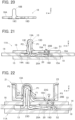
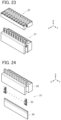
- FIG. 23 shows a connector assembly according to Embodiment 3 before fitting.
- This connector assembly is obtained by using a first connector 31 in place of the first connector 11 in the connector assembly of Embodiment 1, and the second connector 21 used in Embodiment 1 is fitted to the first connector 31.
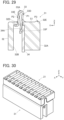
- the first connector 31 includes a first insulator 32 made of an insulating material.
- a plurality of first contacts 33 are disposed on the -Z direction side from the first insulator 32, and a circuit board 34 is disposed on the -Z direction side from the plurality of first contacts 33.
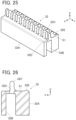
- the first insulator 32 includes an insulator body 32A of rectangular cuboid shape elongated in the Y direction.
- the insulator body 32A includes: a groove portion 32B extending in the Y direction over the entire length of the insulator body 32A and opening toward the -Z direction; and a first exposed surface S1 extending along an XY plane and facing the +Z direction.
- a plurality of projections 32C aligned in the Y direction and projecting in the +Z direction are formed on the first exposed surface S1.
- a plurality of through-holes 32D are each formed between adjacent projections 32C to penetrate the first exposed surface S1 in the Z direction and communicate with the groove portion 32B as shown in FIG. 26 .
- the first exposed surface S1 is provided at its -X directional end with a plurality of protuberance portions 32E aligned in the Y direction and projecting in the +Z direction.
- the plurality of protuberance portions 32E are situated at the same Y-directional positions as the plurality of through-holes 32D, and the plurality of through-holes 32D and the plurality of protuberance portions 32E correspond to the plurality of first contacts 33.
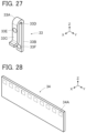
- the first contact 33 is formed from a band-shaped plate member that is made of a conductive material such as metal and that is bent, and the first contact 33 includes a retention projection 33Abent in a U shape and extending in the Z direction.
- the retention projection 33A has a lateral surface 33B facing the -X direction and a lateral surface 33C facing the +X direction, and the lateral surface 33B is provided at its +Z directional end with a hook portion 33D protruding in a right angle shape or a chevron shape and facing the -X direction and the -Z direction.
- the lateral surface 33C is provided with a protrusion portion 33E protruding in the +X direction on the -Z direction side from the hook portion 33D at a position closer to the base portion of the retention projection 33A than the hook portion 33D is.
- the -Z directional end of the lateral surface 33B is provided with a protrusion portion 33F protruding in the -X direction.
- the circuit board 34 is constituted of a so-called flexible printed circuit (FPC) that extends along a YZ plane, and a plurality of connection portions 34A aligned in the Y direction are exposed on the surface, facing the +X direction, of the circuit board 34 at the +Z directional end of the circuit board 34.
- the plurality of connection portions 34A correspond to the plurality of first contacts 33.
- the circuit board 34 is inserted into the groove portion 32B of the insulator body 32A from the -Z direction and fixed to the inner surface, on the -X direction side, of the groove portion 32B; subsequently, the plurality of first contacts 33 are inserted into the groove portion 32B of the insulator body 32A from the -Z direction, and the retention projections 33A of the first contacts 33 are inserted into the corresponding through-holes 32D of the insulator body 32A from the -Z direction.
- the retention projections 33A of the first contacts 33 project in the +Z direction from the first exposed surface S1 of the insulator body 32A, and the protrusion portions 33F protruding in the -X direction at the -Z directional ends of the first contacts 33 make contact, from the +X direction, with the connection portions 34A exposed at the +Z directional end of the circuit board 34.
- a first contacting portion P1 facing the -X direction and the -Z direction is set by the hook portion 33D of the first contact 33
- a second contacting portion P2 facing the +X direction and situated on the -Z direction side from the first contacting portion P1 is set by the protrusion portion 33E of the first contact 33
- a third contacting portion P3 situated on the first exposed surface S1 at a position away from the first contacting portion P1 in the -X direction and facing the +Z direction is set by the protuberance portion 32E of the insulator body 32A.
- the second connector 21 is retained with respect to the first connector 31 owing to the first contacting portion P1, the second contacting portion P2, and the third contacting portion P3 making contact with the second connector 21.
- a +Z directional portion of the retention projection 33A of the first contact 33 of the first connector 31 is inserted into the projection accommodating portion 23D of the second contact 23 of the second connector 21 from the -Z direction, as with Embodiment 1.
- the second connector 21 receives the forces F1 acting in the -X direction and the -Z direction from the first contacting portions P1 of the plurality of first contacts 33 of the first connector 31, the forces F2 acting in the +X direction from the second contacting portions P2 of the plurality of first contacts 33, and the forces F3 acting in the +Z direction from the third contacting portions P3 of the plurality of protuberance portions 32E of the first insulator 32 of the first connector 31.
- the first contacting portion P1 and the second contacting portion P2 of the retention projection 33A of the first contact 33 make contact with the inner surface of the projection accommodating portion 23D of the second contact 23, whereby the first contact 33 is electrically connected to the second contact 23.
- the protrusion portion 33F of the first contact 33 makes contact with the corresponding connection portion 34A of the circuit board 34, so that the first contact 33 is electrically connected to the connection portion 34A of the circuit board 34; thus, the second contact 23 is electrically connected to the connection portion 34A of the circuit board 34 via the first contact 33 in the fitting state between the first connector 31 and the second connector 21.
- Embodiment 3 it is possible to stably maintain the fitting state between the first connector 31 and the second connector 21 and connect the second contacts 23 of the second connector 21 to the connection portions 34A of the circuit board 34 with a simple structure without the use of a dedicated mechanism for locking the fitting state, as with Embodiments 1 and 2.
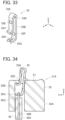
- FIG. 32 shows a first connector 31A used in a connector assembly according to a modification of Embodiment 3.
- the first connector 31A is configured such that, in place of the plurality of first contacts 33, a plurality of first contacts 35 are retained in the first insulator 32, and in place of the circuit board 34, a plurality of cables 36 are connected to the plurality of first contacts 35 in the first connector 31 used in Embodiment 3.
- the first contact 35 is formed in such a manner that a cable connecting portion 35G extends in the +X direction from the -Z directional end of the lateral surface 33B, on the -X direction side, of the retention projection 33A and a cutout 35H is formed in the cable connecting portion 35G to open toward the +X direction.
- the cable 36 has a structure in which the outer periphery of a conductor portion 36A is covered with an insulating coating portion 36B.
- the conductor portion 36A is electrically connected to the first contact 35 by being press-fitted into the cutout 35H of the cable connecting portion 35G of the first contact 35.
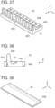
- the first connector 41 includes a first insulator 42 made of an insulating material.
- a plurality of first contacts 43 are disposed on the -Z direction side from the first insulator 42, and a circuit board 44 is disposed on the -Z direction side from the plurality of first contacts 43.
- the top surface, facing the +Z direction, of the flat plate portion 42A is provided with a plurality of through-holes 42D that are aligned in the Y direction on the -X direction side from the plurality of projections 42B and penetrate the flat plate portion 42A in the Z direction.
- the plurality of through-holes 42D are situated at the same Y-directional positions as the plurality of through-holes 42C, and the plurality of through-holes 42C and the plurality of through-holes 42D correspond to the plurality of first contacts 43.
- the through-hole 42C and the through-hole 42D that are situated at the same Y-directional position communicate with each other in a -Z directional portion of the flat plate portion 42A.
- the circuit board 44 is constituted of a so-called flexible printed circuit (FPC) that extends along an XY plane, and a plurality of connection portions 44A aligned in the Y direction are exposed on the surface, facing the +Z direction, of the circuit board 44 at the -X directional end of the circuit board 44.
- the plurality of connection portions 44A correspond to the plurality of first contacts 43.
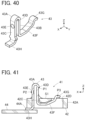
- the first contact 43 is formed from a band-shaped plate member that is made of a conductive material such as metal and that is bent, and the first contact 43 includes a retention projection 43A bent in a U shape and extending in the Z direction.
- the retention projection 43A has a lateral surface 43B facing the -X direction and a lateral surface 43C facing the +X direction, and the lateral surface 43B is provided at its +Z directional end with a hook portion 43D protruding in a right angle shape or a chevron shape and facing the -X direction and the -Z direction.
- the lateral surface 43C is provided with a protrusion portion 43E protruding in the +X direction on the -Z direction side from the hook portion 43D at a position closer to the base portion of the retention projection 43A than the hook portion 43D is.
- a cantilever portion 43F extends in the -X direction and the +Z direction from the -Z directional end of the lateral surface 43B, and the -X directional end of the cantilever portion 43F is provided with a curved portion 43G curving in a convex shape toward the +Z direction.
- connection portion 43H extends in the +X direction from the -Z directional end of the lateral surface 43C.
- the retention projection 43A of the first contact 43 is inserted into the corresponding through-hole 42C of the first insulator 42 from the -Z direction. Since the cantilever portion 43F of the first contact 43 extends in the -X direction and the +Z direction from the -Z directional end of the lateral surface 43B, when the retention projection 43A is inserted into the through-hole 42C of the first insulator 42, the curved portion 43G formed at the -X directional end of the cantilever portion 43F projects in the +Z direction from the first exposed surface S1 through the through-hole 42D of the first insulator 42.
- connection portions 43H of the plurality of first contacts 43 are connected to the plurality of connection portions 44A of the circuit board 44 by soldering or other means.
- a first contacting portion P1 facing the -X direction and the -Z direction is set by the hook portion 43D of the first contact 43
- a second contacting portion P2 facing the +X direction and situated on the -Z direction side from the first contacting portion P1 is set by the protrusion portion 43E
- a third contacting portion P3 situated on the first exposed surface S1 at a position away from the first contacting portion P1 in the -X direction and facing the +Z direction is set by the curved portion 43G.
- the second connector 21 is retained with respect to the first connector 41 owing to the first contacting portion P1, the second contacting portion P2, and the third contacting portion P3 making contact with the second connector 21.
- a +Z directional portion of the retention projection 43A of the first contact 43 of the first connector 41 is inserted into the projection accommodating portion 23D of the second contact 23 of the second connector 21 from the -Z direction, and the first contacting portion P1 and the second contacting portion P2 set at the retention projection 43A separately make contact with the inner surface of the projection accommodating portion 23D of the second contact 23, as with Embodiment 1.
- the third contacting portion P3 set at the curved portion 43G of the first contact 43 projecting in the +Z direction from the first exposed surface S1 through the through-hole 42D of the first insulator 42 makes contact with the bottom surface of the step portion 23G of the second contact 23.
- the second connector 21 receives the forces F1 acting in the -X direction and the -Z direction from the first contacting portions P1 of the plurality of first contacts 43 of the first connector 41, the forces F2 acting in the +X direction from the second contacting portions P2 thereof, and the forces F3 acting in the +Z direction from the third contacting portions P3 thereof.
- the first contacting portion P1 and the second contacting portion P2 of the retention projection 43A of the first contact 43 make contact with the inner surface of the projection accommodating portion 23D of the second contact 23, and the third contacting portion P3 of the curved portion 43G of the first contact 43 makes contact with the bottom surface of the step portion 23G of the second contact 23, whereby the first contact 43 is electrically connected to the second contact 23.
- the connection portion 43H of the first contact 43 makes contact with the connection portion 44A of the circuit board 44, so that the second contact 23 is electrically connected to the connection portion 44A of the circuit board 44 via the first contact 43 in the fitting state between the first connector 41 and the second connector 21.
- Embodiment 4 it is possible to stably maintain the fitting state between the first connector 41 and the second connector 21 and connect the second contacts 23 of the second connector 21 to the connection portions 44A of the circuit board 44 with a simple structure without the use of a dedicated mechanism for locking the fitting state, as with Embodiments 1 to 3.
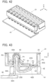
- FIG. 44 shows a connector assembly according to Embodiment 5 before fitting.
- the connector assembly is composed of a first connector 51 and a second connector 61 to be fitted to each other.
- the first connector 51 includes: a first insulator 52 made of an insulating material; and a pair of the first contacts 43 and a plurality of third contacts 53 that are retained in the first insulator 52.
- the pair of first contacts 43 and the plurality of third contacts 53 are attached to the circuit board 44.
- the second connector 61 includes: a second insulator 62 made of an insulating material; and a pair of the second contacts 23 and a plurality of fourth contacts 63 that are retained in the second insulator 62.
- the pair of first contacts 43 and the plurality of third contacts 53 are aligned at the same alignment pitch in the Y direction as the pair of second contacts 23 and the plurality of fourth contacts 63.
- FIG. 45 is an exploded perspective view of the first connector 51.
- the pair of first contacts 43 are disposed on the -Z direction side from the first insulator 52
- the plurality of third contacts 53 are disposed on the -Z direction side from the pair of first contacts 43
- the circuit board 44 is disposed on the -Z direction side from the plurality of third contacts 53.
- the first contact 43 and the circuit board 44 herein are identical to those used in Embodiment 4 and shown in FIGS. 40 and 39 , respectively. However, the first contacts 43 are disposed only at two positions, i.e., at the +Y and -Y directional ends of the first connector 51, and the plurality of third contacts 53 are disposed between the pair of first contacts 43.
- the first insulator 52 includes a flat plate portion 52A elongated in the Y direction along an XY plane and a first exposed surface S1 formed by the top surface, on the +Z direction side, of the flat plate portion 52A.
- a plurality of through-holes 52B aligned in the Y direction and penetrating the flat plate portion 52A in the Z direction are formed on the +X direction side of the flat plate portion 52A, and a plurality of through-holes 52C aligned in the Y direction and penetrating the flat plate portion 52A in the Z direction are formed on the -X direction side of the flat plate portion 52A.
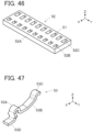
- the third contact 53 is configured to have, in place of the retention projection 43A extending in the Z direction, a U-shaped portion 53A with a small height in the Z direction in the first contact 43 shown in FIG. 40 , and otherwise has the same structure as the first contact 43.
- cantilever portion 53B extends in the -X direction and the +Z direction from the -Z directional end of the U-shaped portion 53A, and the -X directional end of the cantilever portion 53B is provided with a curved portion 53C curving in a convex shape toward the +Z direction.
- a connection portion 53D extends in the +X direction from the -Z directional end of the U-shaped portion 53A.
- the retention projections 43A of the pair of first contacts 43 disposed at the opposite ends in the Y direction are inserted from the -Z direction into the corresponding through-holes 52B of the first insulator 52, i.e., the through-holes 52B situated at the opposite ends in the Y direction among the plurality of through-holes 52B.
- the U-shaped portions 53A of the plurality of third contacts 53 are inserted from the -Z direction into the corresponding through-holes 52B of the first insulator 52, i.e., the through-holes 52B other than those situated at the opposite ends in the Y direction among the plurality of through-holes 52B.
- connection portions 43H of the pair of first contacts 43 and the connection portions 53D of the plurality of third contacts 53 are connected to the plurality of connection portions 44A of the circuit board 44 by soldering or other means.
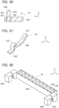
- the second insulator 62 has a structure in which a pair of arm portions 62B extending in the +X direction are joined separately to the opposite ends, in the Y direction, of a body portion 62A of rectangular cuboid shape elongated in the Y direction.
- the pair of arm portions 62B each have a contact accommodating portion 62C of recess shape to accommodate the second contact 23 shown in FIG. 10 .
- the body portion 62A has a plurality of contact accommodating portions 62D of recess shape that are aligned in the Y direction and each accommodate the fourth contact 63.
- the contact accommodating portion 62D is formed by a through-hole penetrating the body portion 62A in the Z direction.
- a partition plate 62E extending along an XZ plane is formed between adjacent contact accommodating portions 62D.
- the fourth contact 63 is formed from a band-shaped plate member made of a conductive material such as metal and is bent in a U shape opening toward the +Z direction.
- the -Z directional end of the fourth contact 63 is provided with a flat plate portion 63A extending along an XY plane and constituting a bottom portion of the U shape.
- the second connector 61 is assembled by inserting the second contacts 23 into the contact accommodating portions 62C of the pair of arm portions 62B of the second insulator 62 from the +Z direction and inserting the fourth contacts 63 into the plurality of contact accommodating portions 62D of the body portion 62A from the +Z direction.
- a +Z directional portion of the retention projection 43A of the first contact 43 of the first connector 51 is inserted into the projection accommodating portion 23D of the second contact 23 of the second connector 61 from the -Z direction, and a first contacting portion P1 and a second contacting portion P2 set at the retention projection 43A separately make contact with the inner surface of the projection accommodating portion 23D of the second contact 23, as with Embodiment 1.
- the curved portion 43G formed at the end of the cantilever portion 43F of the first contact 43 projects in the +Z direction from the first exposed surface S1 through the corresponding through-hole 52C of the first insulator 52, and a third contacting portion P3 set at the curved portion 43G makes contact with the bottom surface of the step portion 23G of the second contact 23.
- the U-shaped portion 53A of the third contact 53 of the first connector 51 is inserted into the corresponding through-hole 52B of the second connector 61 from the -Z direction, and the curved portion 53C formed at the end of the cantilever portion 53B of the third contact 53 projects in the +Z direction from the first exposed surface S1 through the corresponding through-hole 52C of the first insulator 52.
- a third contacting portion P3 is set also by the surface, facing the +Z direction, of the curved portion 53C, and the third contacting portion P3 of the curved portion 53C makes contact with the bottom surface of the flat plate portion 63A of the corresponding fourth contact 63.
- the second connector 61 receives the forces F1 acting in the -X direction and the -Z direction from the first contacting portions P1 of the pair of first contacts 43 of the first connector 51, the forces F2 acting in the +X direction from the second contacting portions P2 of the pair of first contacts 43 of the first connector 51, and the forces F3 acting in the +Z direction from the third contacting portions P3 of the pair of first contacts 43 of the first connector 51 and the third contacting portions P3 of the plurality of third contacts 53 thereof.
- the first contacting portions P1 and the second contacting portions P2 of the retention projections 43A of the first contacts 43 make contact with the inner surfaces of the projection accommodating portions 23D of the second contacts 23, and the third contacting portions P3 of the curved portions 43G of the first contacts 43 make contact with the bottom surfaces of the step portions 23G of the second contacts 23, whereby the pair of first contacts 43 are electrically connected to the corresponding second contacts 23.
- the third contacting portions P3 of the third contacts 53 make contact with the bottom surfaces of the flat plate portions 63A of the fourth contacts 63, whereby the plurality of third contacts 53 are electrically connected to the corresponding fourth contacts 63.
- connection portions 43H of the pair of first contacts 43 of the first connector 51 and the connection portions 53D of the plurality of third contacts 53 thereof make contact with the plurality of connection portions 44A of the circuit board 44, so that the pair of second contacts 23 and the plurality of fourth contacts 63 of the second connector 61 are electrically connected to the corresponding connection portions 44A of the circuit board 44 via the pair of first contacts 43 and the plurality of third contacts 53 in the fitting state between the first connector 51 and the second connector 61.
- Embodiment 5 it is possible to stably maintain the fitting state between the first connector 51 and the second connector 61 and connect the pair of second contacts 23 and the plurality of fourth contacts 63 of the second connector 61 to the corresponding connection portions 44A of the circuit board 44 with a simple structure without the use of a dedicated mechanism for locking the fitting state, as with Embodiments 1 to 4.
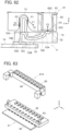
- FIG. 53 shows a connector assembly according to Embodiment 6 before fitting.
- the connector assembly is composed of a first connector 71 and a second connector 81 to be fitted to each other.
- the first connector 71 includes: a first insulator 72 made of an insulating material; and a pair of first contacts 73 and a plurality of the third contacts 53 that are retained in the first insulator 72.
- the pair of first contacts 73 and the plurality of third contacts 53 are attached to a circuit board 74.
- the second connector 81 includes: a second insulator 82 made of an insulating material; and a pair of second contacts 83 and a plurality of the fourth contacts 63 that are retained in the second insulator 82.
- the pair of first contacts 73 and the plurality of third contacts 53 are aligned at the same alignment pitch in the Y direction as the pair of second contacts 83 and the plurality of fourth contacts 63.
- FIG. 54 is an exploded perspective view of the first connector 71.
- the pair of first contacts 73 are disposed on the -Z direction side from the first insulator 72
- the plurality of third contacts 53 are disposed on the -Z direction side from the pair of first contacts 73
- the circuit board 74 is disposed on the -Z direction side from the plurality of third contacts 53.
- the third contact 53 herein is identical to that used in Embodiment 5 and shown in FIG. 47 .
- the plurality of third contacts 53 are disposed between the pair of first contacts 73.
- the first insulator 72 includes a flat plate portion 72A elongated in the Y direction along an XY plane and a first exposed surface S1 formed by the top surface, on the +Z direction side, of the flat plate portion 72A.
- a pair of through-holes 72B are formed at the opposite ends in the Y direction to penetrate the flat plate portion 72A in the Z direction, and a plurality of through-holes 72C are formed to be aligned in the Y direction between the pair of through-holes 72B and penetrate the flat plate portion 72A in the Z direction.
- a plurality of through-holes 72D are formed to be aligned in the Y direction and penetrate the flat plate portion 72A in the Z direction.
- the pair of through-holes 72B are situated at the same X-directional position as the plurality of through-holes 72C, and the plurality of through-holes 72C are situated at the same Y-directional positions as the plurality of the through-holes 72D.
- the pair of through-holes 72B, the plurality of through-holes 72C, and the plurality of through-holes 72D are aligned at the same alignment pitch in the Y direction.
- the pair of through-holes 72B correspond to the pair of first contacts 73
- the plurality of through-holes 72C and the plurality of through-holes 72D correspond to the plurality of third contacts 53.
- the circuit board 74 is constituted of a so-called flexible printed circuit (FPC) that extends along an XY plane.
- FPC flexible printed circuit
- a pair of connection portions 74A disposed at the opposite ends in the Y direction are exposed on the surface, facing the +Z direction, of the circuit board 74, and a plurality of connection portions 74B aligned in the Y direction between the pair of connection portions 74A are exposed on the same surface.
- the pair of connection portions 74A and the plurality of connection portions 74B are aligned at the same alignment pitch in the Y direction as the pair of through-holes 72B, the plurality of through-holes 72C, and the plurality of through-holes 72D of the first insulator 72.
- connection portions 74A correspond to the pair of first contacts 73
- the plurality of connection portions 74B correspond to the plurality of third contacts 53.
- the first contact 73 is formed from a band-shaped plate member that is made of a conductive material such as metal and that is bent, and the first contact 73 includes a retention projection 73A bent in a U shape and extending in the Z direction.
- the retention projection 73A has a lateral surface 73B facing the -X direction and a lateral surface 73C facing the +X direction, and the lateral surface 73B is provided at its +Z directional end with a hook portion 73D protruding in a right angle shape or a chevron shape and facing the -X direction and the -Z direction.
- the lateral surface 73C is provided with a protrusion portion 73E protruding in the +X direction on the -Z direction side from the hook portion 73D at a position closer to the base portion of the retention projection 73A than the hook portion 73D is.
- connection portions 73F extend separately in the -X direction and the +X direction from the -Z directional ends of the lateral surfaces 73B and 73C.
- the retention projections 73A of the pair of first contacts 73 disposed at the opposite ends in the Y direction are inserted into the corresponding through-holes 72B of the first insulator 72 from the -Z direction.
- the U-shaped portions 53A of the plurality of third contacts 53 are inserted into the corresponding through-holes 72C of the first insulator 72 from the -Z direction.
- connection portions 73F of the pair of first contacts 73 are connected to the pair of connection portions 74A of the circuit board 74 by soldering or other means, and the connection portions 53D of the plurality of third contacts 53 are connected to the plurality of connection portions 74B of the circuit board 74 by soldering or other means.
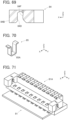
- the second insulator 82 has a structure in which a pair of arm portions 82B extending in the +X direction are joined separately to the opposite ends, in the Y direction, of a body portion 82A of rectangular cuboid shape elongated in the Y direction.
- the pair of arm portions 82B each have a contact accommodating portion 82C of recess shape to accommodate the second contact 83.
- the body portion 82A has a plurality of contact accommodating portions 82D of recess shape that are aligned in the Y direction and each accommodate the fourth contact 63 used in Embodiment 5 and shown in FIG. 49 .
- the contact accommodating portion 82D is formed by a through-hole penetrating the body portion 82A in the Z direction.
- a partition plate 82E extending along an XZ plane is formed between adjacent contact accommodating portions 82D.
- the second contact 83 is formed from a band-shaped plate member made of a conductive material such as metal and includes a U-shaped portion 83A curved in a U shape opening toward the -Z direction.
- the U-shaped portion 83A includes a first extension portion 83B extending along a YZ plane on the -X direction side and a second extension portion 83C extending along a YZ plane on the +X direction side.
- a projection accommodating portion 83D of recess shape is formed inside the U-shaped portion 83A to accommodate the retention projection 73A of the first contact 73.
- the surface, on the +X direction side, of the first extension portion 83B facing the projection accommodating portion 83D is provided with a receiving portion 83E formed by a concavity for receiving the hook portion 73D of the first contact 73.
- the second contact 83 includes a rising portion 83F bent toward the -X direction from the -Z directional end of the first extension portion 83B and rising in the +Z direction and a rising portion 83G bent toward the +X direction from the -Z directional end of the second extension portion 83C and rising in the +Z direction.
- the second connector 81 is assembled by inserting the second contacts 83 into the contact accommodating portions 82C of the pair of arm portions 82B of the second insulator 82 from the +Z direction and inserting the fourth contacts 63 into the plurality of contact accommodating portions 82D of the body portion 82A from the +Z direction.
- a +Z directional portion of the retention projection 73A of the first contact 73 of the first connector 71 is inserted into the projection accommodating portion 83D of the second contact 83 of the second connector 81 from the -Z direction, and a first contacting portion P1 set by the hook portion 73D of the retention projection 73A and a second contacting portion P2 set by the protrusion portion 73E separately make contact with the inner surface of the projection accommodating portion 83D of the second contact 83, as with Embodiment 1.
- a third contacting portion P3 set by the curved portion 53C formed at the end of the cantilever portion 53B of each of the plurality of third contacts 53 makes contact with the bottom surface of the flat plate portion 63A of the corresponding fourth contact 63.
- the second connector 81 receives forces F1 acting in the -X direction and the -Z direction from the first contacting portions P1 of the pair of first contacts 73 of the first connector 71, forces F2 acting in the +X direction from the second contacting portions P2 of the pair of first contacts 73 of the first connector 71, and forces F3 acting in the +Z direction from the third contacting portions P3 of the plurality of third contacts 53 of the first connector 71.
- the first contacting portions P1 and the second contacting portions P2 of the retention projections 73A of the pair of first contacts 73 make contact with the inner surfaces of the projection accommodating portions 83D of the second contacts 83, whereby the pair of first contacts 73 are electrically connected to the corresponding second contacts 83.
- the third contacting portions P3 of the plurality of third contacts 53 make contact with the bottom surfaces of the flat plate portions 63A of the fourth contacts 63, whereby the plurality of third contacts 53 are electrically connected to the corresponding fourth contacts 63.
- connection portions 73F of the pair of first contacts 73 of the first connector 71 are connected to the pair of connection portions 74A of the circuit board 74, and the connection portions 53D of the plurality of third contacts 53 are connected to the plurality of connection portions 74B of the circuit board 74, so that the pair of second contacts 83 and the plurality of fourth contacts 63 of the second connector 81 are electrically connected to the pair of connection portions 74A and the plurality of connection portions 74B of the circuit board 74 via the pair of first contacts 73 and the plurality of third contacts 53 in the fitting state between the first connector 71 and the second connector 81.
- Embodiment 6 it is possible to stably maintain the fitting state between the first connector 71 and the second connector 81 and connect the pair of second contacts 83 and the plurality of fourth contacts 63 of the second connector 81 to the pair of connection portions 74A and the plurality of connection portions 74B of the circuit board 74 with a simple structure without the use of a dedicated mechanism for locking the fitting state, as with Embodiments 1 to 5.
- FIG. 63 shows a connector assembly according to Embodiment 7 before fitting.
- the connector assembly is composed of a first connector 91 and a second connector 81A to be fitted to each other.
- the first connector 91 includes a first insulator 92 made of an insulating material and a plurality of first contacts 93 retained in the first insulator 92.
- the plurality of first contacts 93 are attached to the circuit board 44.
- the second connector 81A includes a second insulator 84 made of an insulating material and a plurality of second contacts 85 retained in the second insulator 84.
- the plurality of first contacts 93 and the plurality of second contacts 85 are aligned at the same alignment pitch in the Y direction.
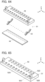
- FIG. 64 is an exploded perspective view of the first connector 91.
- the plurality of first contacts 93 are disposed on the -Z direction side from the first insulator 92, and the circuit board 44 is disposed on the -Z direction side from the plurality of first contacts 93.
- the first contact 93 herein has the same structure as the third contact 53 used in Embodiment 5 and shown in FIG. 47 , and the circuit board 44 herein is identical to that used in Embodiment 4 and shown in FIG. 39 .
- the first insulator 92 includes a flat plate portion 92A elongated in the Y direction along an XY plane and a first exposed surface S1 formed by the top surface, on the +Z direction side, of the flat plate portion 92A.
- a pair of retention projections 92B disposed at the opposite ends in the Y direction and projecting in the +Z direction from the first exposed surface S1 are formed on the +X direction side of the flat plate portion 92A.
- a plurality of through-holes 92C aligned in the Y direction and penetrating the flat plate portion 92A in the Z direction are formed between the pair of retention projections 92B.
- a plurality of through-holes 92D aligned in the Y direction and penetrating the flat plate portion 92A in the Z direction are formed on the -X direction side of the flat plate portion 92A.
- the plurality of through-holes 92C and the plurality of through-holes 92D are situated at the same Y-directional positions and aligned at the same alignment pitch in the Y direction.
- the plurality of through-holes 92C and the plurality of through-holes 92D correspond to the plurality of first contacts 93.
- the retention projection 92B of the first insulator 92 has a lateral surface 92E facing the -X direction and a lateral surface 92F facing the +X direction, and the lateral surface 92E is provided at its +Z directional end with a hook portion 92G protruding in a right angle shape or a chevron shape and facing the -X direction and the -Z direction.
- the lateral surface 92F is provided with a protrusion portion 92H protruding in the +X direction on the -Z direction side from the hook portion 92G at a position closer to the base portion of the retention projection 92B than the hook portion 92G is.
- the first contact 93 herein has the same structure as the third contact 53 used in Embodiment 5 and shown in FIG. 47 . That is, the first contact 93 is formed from a band-shaped plate member made of a conductive material such as metal and includes a U-shaped portion 93A.
- a cantilever portion 93B extends in the -X direction and the +Z direction from the -Z directional end of the U-shaped portion 93A, and the -X directional end of the cantilever portion 93B is provided with a curved portion 93C curving in a convex shape toward the +Z direction.
- a connection portion 93D extends in the +X direction from the -Z directional end of the U-shaped portion 93A.
- the U-shaped portions 93A of the plurality of first contacts 93 are inserted into the corresponding through-holes 92C of the first insulator 92 from the -Z direction, and in this state, the connection portions 93D of the plurality of first contacts 93 are connected to the plurality of connection portions 44A of the circuit board 44 by soldering or other means.
- a first contacting portion P1 facing the -X direction and the -Z direction is set by the hook portion 92G of the retention projection 92B of the first insulator 92, and a second contacting portion P2 facing the +X direction and situated on the -Z direction side from the first contacting portion P1 is set by the protrusion portion 92H of the retention projection 92B.
- the U-shaped portion 93A of the first contact 93 is inserted into the corresponding through-hole 92C of the first insulator 92, so that the curved portion 93C formed at the end of the cantilever portion 93B of the first contact 93 projects in the +Z direction from the first exposed surface S 1 through the corresponding through-hole 92D of the first insulator 92.
- a third contacting portion P3 facing the +Z direction is set by this curved portion 93C.
- the second insulator 84 has a structure in which a pair of arm portions 84B extending in the +X direction are joined separately to the opposite ends, in the Y direction, of a body portion 84A of rectangular cuboid shape elongated in the Y direction.
- the pair of arm portions 84B each have a projection accommodating portion 84C of recess shape to accommodate the retention projection 92B of the first insulator 92.
- the body portion 84A has a plurality of contact accommodating portions 84D of recess shape that are aligned in the Y direction and each accommodate the second contact 85.
- the contact accommodating portion 84D is formed by a through-hole penetrating the body portion 84A in the Z direction.
- a partition plate 84E extending along an XZ plane is formed between adjacent contact accommodating portions 84D.
- the projection accommodating portion 84C of the arm portion 84B is constituted of a recess portion opening toward the -Z direction, and the inner surface of the projection accommodating portion 84C on the -X direction side is provided with a receiving portion 84F formed by a concavity for receiving the hook portion 92G of the retention projection 92B.
- the second connector 81A is assembled by inserting the second contacts 85 into the plurality of contact accommodating portions 84D of the body portion 84A of the second insulator 84 from the +Z direction.
- the second contact 85 herein has the same structure as the fourth contact 63 used in Embodiment 5 and shown in FIG. 49 . That is, the second contact 85 is formed from a band-shaped plate member made of a conductive material such as metal and is bent in a U shape opening toward the +Z direction. The -Z directional end of the second contact 85 is provided with a flat plate portion 85A extending along an XY plane and constituting a bottom portion of the U shape.
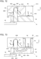
- a +Z directional portion of the retention projection 92B of the first connector 91 is inserted into the projection accommodating portion 84C of the arm portion 84B of the second connector 81A from the -Z direction, the first contacting portion P1 set by the hook portion 92G of the retention projection 92B makes contact with the receiving portion 84F of the projection accommodating portion 84C, and the second contacting portion P2 set by the protrusion portion 92H of the retention projection 92B makes contact with the inner surface of the projection accommodating portion 84C.
- the third contacting portion P3 set by the curved portion 93C formed at the end of the cantilever portion 93B of each of the plurality of first contacts 93 makes contact with the bottom surface of the flat plate portion 85A of the corresponding second contact 85, as shown in FIG. 73 .
- the second connector 81A receives forces F1 acting in the -X direction and the -Z direction from the first contacting portions P1 of the pair of retention projections 92B of the first connector 91, forces F2 acting in the +X direction from the second contacting portions P2 of the pair of retention projections 92B of the first connector 91, and forces F3 acting in the +Z direction from the third contacting portions P3 of the plurality of first contacts 93 of the first connector 91.
- the third contacting portions P3 of the plurality of first contacts 93 make contact with the bottom surfaces of the flat plate portions 85A of the second contacts 85, whereby the plurality of first contacts 93 are electrically connected to the corresponding second contacts 85.
- connection portions 93D of the plurality of first contacts 93 of the first connector 91 are connected to the plurality of connection portions 44A of the circuit board 44, so that the plurality of second contacts 85 of the second connector 81A are electrically connected to the plurality of connection portions 44A of the circuit board 44 via the plurality of first contacts 93 in the fitting state between the first connector 91 and the second connector 81A.
- Embodiment 7 it is possible to stably maintain the fitting state between the first connector 91 and the second connector 81A and connect the plurality of second contacts 85 of the second connector 81A to the plurality of connection portions 44A of the circuit board 44 with a simple structure without the use of a dedicated mechanism for locking the fitting state, as with Embodiments 1 to 6.
- the tab sheet 14 is not used in Embodiments 3 to 7; however, by attaching the first connector 31, 31A, 41, 51, 71, 91 to the tab sheet 14 made of, for instance, cloth of a garment as in Embodiments 1 and 2, the first connector 31, 31A, 41, 51, 71, 91 may be used as a garment-side connector, and the second connector 21, 61, 81, 81A may be used as a module-side connector.
- the second connector 21, 61, 81, 81Ain Embodiments 1 to 7 may be used as a garment-side connector to be attached to a garment, and the first connector 11, 11A, 31, 31A, 41, 51, 71, 91 in those embodiments may be used as a module-side connector to be fitted to the garment-side connector.
- circuit board 17, 19, 44, 74 extends along an XY plane in parallel to the first exposed surface S1 of the first connector 11, 11A, 41, 51, 71, 91 in Embodiments 1, 2, and 4 to 7, the invention is not limited thereto, and use may be made of a circuit board extending in a fitting direction along a YZ plane as with the circuit board 34 in Embodiment 3. Further, the first contact 13, 43, 73, 93 in Embodiments 1, 2, and 4 to 7 may be connected to a cable in place of the circuit board, as with the modification of Embodiment 3.
Landscapes
- Coupling Device And Connection With Printed Circuit (AREA)
- Professional, Industrial, Or Sporting Protective Garments (AREA)
- Details Of Connecting Devices For Male And Female Coupling (AREA)
Abstract
Description
- The present invention relates to a connector assembly, particularly to a connector assembly used to fit a module-side connector of a wearable device to a garment-side connector to establish electrical connection therebetween.
- In recent years, attention has been drawn to so-called smart clothes that can obtain user's biological data such as the heart rate and the body temperature only by being worn by the user. Such smart clothes have an electrode disposed at a measurement site, and when a wearable device serving as a measurement device is electrically connected to the electrode, biological data can be transmitted to the wearable device.
- The electrode and the wearable device can be interconnected by, for instance, use of a connector connected to a conductor drawn from the electrode.
- As a connector of this type, for example,
JP 2019-87515 A FIG. 74 . The connector includes a garment-side connector portion 1 to be attached to a garment and a module-side connector portion 2 to be fitted to the garment-side connector portion 1. The garment-side connector portion 1 includes a module-sideconnector accommodating portion 3 of recess shape and a plurality of garment-side contacts 4 aligned within the module-sideconnector accommodating portion 3, and the garment-side contacts 4 are connected to conductor portions of aconductive sheet 5 disposed on the garment. The module-side connector portion 2 includes a plurality of module-side contacts 6 aligned to correspond to the garment-side contacts 4. - When the module-
side connector portion 2 is accommodated into the module-sideconnector accommodating portion 3 of the garment-side connector portion 1, the module-side connector portion 2 is fitted to the garment-side connector portion 1, and the module-side contacts 6 are connected to the garment-side contacts 4. - In addition, when a
locking portion 7 of protrusion shape formed in the module-sideconnector accommodating portion 3 of the garment-side connector portion 1 is fitted to a to-be-locked portion 8 of recess shape formed in the module-side connector portion 2, the fitting state between the garment-side connector portion 1 and the module-side connector portion 2 can be locked. - However, this configuration requires formation of the
locking portion 7 in the garment-side connector portion 1 and the to-be-lockedportion 8 in the module-side connector portion 2 to prevent the module-side connector portion 2 from coming off the module-sideconnector accommodating portion 3 of the garment-side connector portion 1 and retain the fitting state between the garment-side connector portion 1 and the module-side connector portion 2, resulting in a complex structure of the connector. - The present invention has been made to overcome such a conventional problem and provide a connector assembly that can stably maintain a fitting state even with a simple structure.
- A connector assembly according to the present invention is one including a first connector and a second connector that are fitted to each other along a fitting direction such that a second contact of the second connector is electrically connected to a first contact of the first connector,
- wherein the first connector includes a first exposed surface facing the second connector and a retention projection projecting in the fitting direction from the first exposed surface toward the second connector,
- the second connector includes a second exposed surface facing the first connector and a projection accommodating portion of recess shape which is formed at the second exposed surface and in which at least a part of the retention projection is accommodated,
- the first connector includes: a first contacting portion disposed on a lateral surface of the retention projection; a second contacting portion disposed on a lateral surface of the retention projection opposite to the lateral surface having the first contacting portion thereon, at a position closer to a base portion of the retention projection than the first contacting portion is; and a third contacting portion disposed on the first exposed surface at a position away from the lateral surface, having the first contacting portion thereon, of the retention projection in an opposite direction from the second contacting portion, and
- when the first connector and the second connector are fitted to each other, at least a part of the retention projection is accommodated in the projection accommodating portion, the first contacting portion and the second contacting portion separately make contact with an inner surface of the projection accommodating portion, and the third contacting portion makes contact with the second exposed surface, whereby a fitting state between the first connector and the second connector is maintained.
-
-
FIG. 1 is a perspective view showing a connector assembly ofEmbodiment 1 before fitting. -
FIG. 2 is an exploded perspective view of a first connector inEmbodiment 1. -
FIG. 3 is a perspective view showing a bottom insulator used in the first connector inEmbodiment 1. -
FIG. 4 is a perspective view showing a first contact used in the first connector inEmbodiment 1. -
FIG. 5 is a perspective view of a circuit board used in the first connector inEmbodiment 1, as viewed from an obliquely lower position. -
FIG. 6 is a perspective view showing a top insulator used in the first connector inEmbodiment 1. -
FIG. 7 is a cross-sectional view showing the top insulator used in the first connector inEmbodiment 1. -
FIG. 8 is a cross-sectional view showing the first connector inEmbodiment 1. -
FIG. 9 is a perspective view showing a second insulator used in a second connector inEmbodiment 1. -
FIG. 10 is a perspective view showing a second contact used in the second connector inEmbodiment 1. -
FIG. 11 is a cross-sectional view showing the second connector inEmbodiment 1. -
FIG. 12 is a perspective view showing the connector assembly ofEmbodiment 1 in a fitting state. -
FIG. 13 is a partial cross-sectional view showing the connector assembly ofEmbodiment 1 in the fitting state. -
FIG. 14 is an enlarged view of an important part ofFIG. 13 . -
FIG. 15 is a perspective view showing a connector assembly ofEmbodiment 2 before fitting. -
FIG. 16 is an exploded perspective view of a first connector inEmbodiment 2. -
FIG. 17 is a perspective view showing a circuit board used in the first connector inEmbodiment 2. -
FIG. 18 is a perspective view showing an auxiliary contact used in the first connector inEmbodiment 2. -
FIG. 19 is a perspective view showing a top insulator used in the first connector inEmbodiment 2. -
FIG. 20 is a cross-sectional view showing the top insulator used in the first connector inEmbodiment 2. -
FIG. 21 is a cross-sectional view showing the first connector inEmbodiment 2. -
FIG. 22 is a partial cross-sectional view showing the connector assembly ofEmbodiment 2 in a fitting state. -
FIG. 23 is a perspective view showing a connector assembly ofEmbodiment 3 before fitting. -
FIG. 24 is an exploded perspective view of a first connector inEmbodiment 3. -
FIG. 25 is a perspective view showing a first insulator used in the first connector inEmbodiment 3. -
FIG. 26 is a cross-sectional view showing the first insulator used in the first connector inEmbodiment 3. -
FIG. 27 is a perspective view showing a first contact used in the first connector inEmbodiment 3. -
FIG. 28 is a perspective view showing a circuit board used in the first connector inEmbodiment 3. -
FIG. 29 is a cross-sectional view showing the first connector inEmbodiment 3. -
FIG. 30 is a perspective view showing the connector assembly ofEmbodiment 3 in a fitting state. -
FIG. 31 is a cross-sectional view showing the connector assembly ofEmbodiment 3 in the fitting state. -
FIG. 32 is a perspective view showing a first connector in a modification ofEmbodiment 3. -
FIG. 33 is a perspective view showing a first contact used in the first connector in the modification ofEmbodiment 3. -
FIG. 34 is a cross-sectional view showing the first connector in the modification ofEmbodiment 3. -
FIG. 35 is a perspective view showing a connector assembly ofEmbodiment 4 before fitting. -
FIG. 36 is an exploded perspective view of a first connector inEmbodiment 4. -
FIG. 37 is a perspective view showing a first insulator used in the first connector inEmbodiment 4. -
FIG. 38 is a cross-sectional view showing the first insulator used in the first connector inEmbodiment 4. -
FIG. 39 is a perspective view showing a circuit board used in the first connector inEmbodiment 4. -
FIG. 40 is a perspective view showing a first contact used in the first connector inEmbodiment 4. -
FIG. 41 is a cross-sectional view showing the first connector inEmbodiment 4. -
FIG. 42 is a perspective view showing the connector assembly ofEmbodiment 4 in a fitting state. -
FIG. 43 is a partial cross-sectional view showing the connector assembly ofEmbodiment 4 in the fitting state. -
FIG. 44 is a perspective view showing a connector assembly ofEmbodiment 5 before fitting. -
FIG. 45 is an exploded perspective view of a first connector inEmbodiment 5. -
FIG. 46 is a perspective view showing a first insulator used in the first connector inEmbodiment 5. -
FIG. 47 is a perspective view showing a third contact used in the first connector inEmbodiment 5. -
FIG. 48 is a perspective view showing a second insulator used in a second connector inEmbodiment 5. -
FIG. 49 is a perspective view showing a fourth contact used in the second connector inEmbodiment 5. -
FIG. 50 is a perspective view showing the connector assembly ofEmbodiment 5 in a fitting state. -
FIG. 51 is a partial cross-sectional view showing the connector assembly ofEmbodiment 5 in the fitting state in a cross section passing through the first contact and the second contact. -
FIG. 52 is a partial cross-sectional view showing the connector assembly ofEmbodiment 5 in the fitting state in a cross section passing through the third contact and the fourth contact. -
FIG. 53 is a perspective view showing a connector assembly ofEmbodiment 6 before fitting. -
FIG. 54 is an exploded perspective view of a first connector inEmbodiment 6. -
FIG. 55 is a perspective view showing a first insulator used in the first connector inEmbodiment 6. -
FIG. 56 is a perspective view showing a circuit board used in the first connector inEmbodiment 6. -
FIG. 57 is a perspective view showing a first contact used in the first connector inEmbodiment 6. -
FIG. 58 is a perspective view showing a second insulator used in a second connector inEmbodiment 6. -
FIG. 59 is a perspective view showing a second contact used in the second connector inEmbodiment 6. -
FIG. 60 is a perspective view showing the connector assembly ofEmbodiment 6 in a fitting state. -
FIG. 61 is a partial cross-sectional view showing the connector assembly ofEmbodiment 6 in the fitting state in a cross section passing through the first contact and the second contact. -
FIG. 62 is a partial cross-sectional view showing the connector assembly ofEmbodiment 6 in the fitting state in a cross section passing through the third contact and the fourth contact. -
FIG. 63 is a perspective view showing a connector assembly ofEmbodiment 7 before fitting. -
FIG. 64 is an exploded perspective view of a first connector inEmbodiment 7. -
FIG. 65 is a perspective view showing a first insulator used in the first connector inEmbodiment 7. -
FIG. 66 is a cross-sectional view showing the first insulator used in the first connector inEmbodiment 7. -
FIG. 67 is a perspective view showing a first contact used in the first connector inEmbodiment 7. -
FIG. 68 is a perspective view showing a second insulator used in a second connector inEmbodiment 7. -
FIG. 69 is a cross-sectional view showing the second insulator used in the second connector inEmbodiment 7. -
FIG. 70 is a perspective view showing a second contact used in the second connector inEmbodiment 7. -
FIG. 71 is a perspective view showing the connector assembly ofEmbodiment 7 in a fitting state. -
FIG. 72 is a partial cross-sectional view showing the connector assembly ofEmbodiment 7 in the fitting state in a cross section passing through a retention projection and a projection accommodating portion. -
FIG. 73 is a partial cross-sectional view showing the connector assembly ofEmbodiment 7 in the fitting state in a cross section passing through the first contact and the second contact. -
FIG. 74 is a perspective view showing a conventional connector. - Embodiments of the present invention are described below based on the accompanying drawings.
-
FIG. 1 shows a connector assembly according toEmbodiment 1 before fitting. The connector assembly is composed of afirst connector 11 and asecond connector 21 to be fitted to each other. For instance, thefirst connector 11 is used as a garment-side connector to be attached to a garment, and thesecond connector 21 is used as a module-side connector to be fitted to thefirst connector 11. - The
first connector 11 includes: afirst insulator 12 made of an insulating material; and a plurality offirst contacts 13 aligned in a predetermined direction and held by thefirst insulator 12. Thefirst insulator 12 is attached to atab sheet 14. - The
second connector 21 includes: asecond insulator 22 made of an insulating material; and a plurality ofsecond contacts 23 aligned in a predetermined direction in the same manner as the plurality offirst contacts 13 of thefirst connector 11 and held by thesecond insulator 22. - The plurality of
first contacts 13 and the plurality ofsecond contacts 23 are aligned in parallel to each other at the same alignment pitch. - For convenience, a direction in which the plurality of
first contacts 13 and the plurality ofsecond contacts 23 are aligned is defined as "Y direction," a direction from thefirst connector 11 to thesecond connector 21 as "+Z direction," and a direction perpendicular to the Y direction and the Z direction as "X direction." The Z direction is a fitting direction in which thesecond connector 21 is fitted to thefirst connector 11. -
FIG. 2 is an exploded perspective view of thefirst connector 11. Thefirst connector 11 includes abottom insulator 15 and atop insulator 16, and these bottom andtop insulators first insulator 12. - The plurality of
first contacts 13 are disposed on the +Z direction side from thebottom insulator 15, and acircuit board 17 is disposed on the +Z direction side from the plurality offirst contacts 13. Further, thetab sheet 14 is disposed on the +Z direction side from thecircuit board 17, and thetop insulator 16 is disposed on the +Z direction side from thetab sheet 14. - The
tab sheet 14 is made of, for instance, cloth of a garment to which thefirst connector 11 is to be attached as the garment-side connector, and thetab sheet 14 has arectangular opening 14A. - As shown in
FIG. 3 , thebottom insulator 15 includes aflat plate portion 15A extending along an XY plane, and a plurality ofcontact supporting portions 15B of protrusion shape are formed to be aligned in the Y direction on the top surface, facing the +Z direction, of theflat plate portion 15A. In addition, a plurality ofprojections 15C are formed to be aligned in the Y direction on the top surface, facing the +Z direction, of theflat plate portion 15A on the -X direction side from the plurality ofcontact supporting portions 15B. A plurality ofcontact insertion portions 15D are each formed by a gap betweenadjacent projections 15C. - The plurality of
contact insertion portions 15D are situated at the same Y-directional positions as the plurality ofcontact supporting portions 15B, and the plurality ofcontact supporting portions 15B and the plurality ofcontact insertion portions 15D correspond to the plurality offirst contacts 13. - The
flat plate portion 15A is provided at its +X directional end with a tabsheet supporting portion 15E extending in the Y direction and protruding in the +Z direction. - As shown in
FIG. 4 , thefirst contact 13 is formed from a band-shaped plate member that is made of a conductive material such as metal and that is bent, and thefirst contact 13 includes aretention projection 13A bent in a U shape and extending in the Z direction. Theretention projection 13A has alateral surface 13B facing the -X direction and alateral surface 13C facing the +X direction, and thelateral surface 13B is provided at its +Z directional end with ahook portion 13D protruding in a right angle shape or a chevron shape and facing the -X direction and the -Z direction. Thelateral surface 13C is provided with aprotrusion portion 13E protruding in the +X direction on the -Z direction side from thehook portion 13D at a position closer to the base portion of theretention projection 13A than thehook portion 13D is. - The -Z directional end of the
lateral surface 13B is provided with abent portion 13F protruding in the -Z direction. Acantilever portion 13G extends in the -X direction from thebent portion 13F. The -X directional end of thecantilever portion 13G is provided with acurved portion 13H curving in a convex shape toward the +Z direction. - As shown in
FIG. 5 , thecircuit board 17 is constituted of, for example, a so-called flexible printed circuit (FPC), and a plurality ofconnection portions 17A aligned in the Y direction are exposed on the bottom surface, facing the -Z direction, of thecircuit board 17 at the +X directional end of thecircuit board 17. The plurality ofconnection portions 17A correspond to the plurality offirst contacts 13. - As shown in
FIG. 6 , thetop insulator 16 includes aflat plate portion 16A extending along an XY plane, and a plurality ofprojections 16B aligned in the Y direction and projecting in the +Z direction are formed on the top surface, facing the +Z direction, of theflat plate portion 16A. A plurality of through-holes 16C penetrating theflat plate portion 16A in the Z direction as shown inFIG. 7 are each formed betweenadjacent projections 16B. In addition, a plurality ofprotuberance portions 16D aligned in the Y direction and projecting in the +Z direction are formed on the top surface, facing the +Z direction, of theflat plate portion 16A on the -X direction side from the plurality ofprojections 16B. - The plurality of
protuberance portions 16D are situated at the same Y-directional positions as the plurality of through-holes 16C, and the plurality of through-holes 16C and the plurality ofprotuberance portions 16D correspond to the plurality offirst contacts 13. - When the
first connector 11 is assembled, as shown inFIG. 8 , theretention projection 13A of thefirst contact 13 is inserted into the corresponding through-hole 16C of thetop insulator 16 from the -Z direction within theopening 14A of thetab sheet 14, and thetab sheet 14 and thecircuit board 17 are sandwiched between theflat plate portion 15A of thebottom insulator 15 and theflat plate portion 16A of thetop insulator 16 such that theconnection portion 17A of thecircuit board 17 is situated on the +Z direction side of thecurved portion 13H of the correspondingfirst contact 13. In this state, thebottom insulator 15 and thetop insulator 16 are fixed to each other. - The
bottom insulator 15 and thetop insulator 16 may be fixed to each other by being adhered to thetab sheet 14 and thecircuit board 17, or alternatively by another method, e.g., by inserting a boss formed to project on one of thebottom insulator 15 and thetop insulator 16 into a through-hole formed in the other thereof and deforming the tip of the boss by heat. - As shown in
FIG. 8 , thefirst contact 13 is retained by thebottom insulator 15 and thetop insulator 16 with thebent portion 13F being situated on thecontact supporting portion 15B of thebottom insulator 15, the -X directional end of thecantilever portion 13G being inserted in thecontact insertion portion 15D of thebottom insulator 15, and thecurved portion 13H being in contact with theconnection portion 17A of thecircuit board 17. - While the
first contact 13 does not have a fixation portion fixed to thebottom insulator 15 and thetop insulator 16, a part of thefirst contact 13 may be fixed to one of thebottom insulator 15 and thetop insulator 16. - In the
first connector 11 configured as above, the top surface, facing the +Z direction, of theflat plate portion 16A of thetop insulator 16 forms a first exposed surface S1 facing thesecond connector 21, and theretention projection 13A of thefirst contact 13 projects in the +Z direction from the first exposed surface S1. - In addition, a first contacting portion P1 facing the -X direction and the -Z direction is set by the
hook portion 13D of thefirst contact 13, a second contacting portion P2 facing the +X direction and situated on the -Z direction side from the first contacting portion P1 is set by theprotrusion portion 13E of thefirst contact 13, and a third contacting portion P3 situated on the first exposed surface S1 at a position away from the first contacting portion P1 in the -X direction and facing the +Z direction is set by theprotuberance portion 16D of thetop insulator 16. - The
second connector 21 is retained with respect to thefirst connector 11 owing to the first contacting portion P1, the second contacting portion P2, and the third contacting portion P3 making contact with thesecond connector 21. - As shown in
FIG. 9 , thesecond insulator 22 has a rectangular cuboid outer shape and includes a plurality of contactaccommodating portions 22A of recess shape aligned in the Y direction and each extending in the X direction and the Z direction. Apartition plate 22B extending along an XZ plane is formed between adjacentcontact accommodating portions 22A. - Each
partition plate 22B is provided with aU-shaped cutout 22C opening toward the -Z direction. - As shown in
FIG. 10 , thesecond contact 23 is formed from a band-shaped plate member that is made of a conductive material such as metal and that is bent, and thesecond contact 23 includes aU-shaped portion 23A curved in a U shape opening toward the -Z direction. TheU-shaped portion 23A includes afirst extension portion 23B extending along a YZ plane on the -X direction side and asecond extension portion 23C extending along a YZ plane on the +X direction side. Aprojection accommodating portion 23D of recess shape is formed inside theU-shaped portion 23A to accommodate theretention projection 13A of thefirst contact 13. The surface, on the +X direction side, of thefirst extension portion 23B facing theprojection accommodating portion 23D is provided with a receivingportion 23E formed by a concavity for receiving thehook portion 13D of thefirst contact 13. - The
second contact 23 has abottom portion 23F extending in the -X direction from the -Z directional end of thefirst extension portion 23B. Thebottom portion 23F is provided with astep portion 23G that goes down in the -Z direction, and a risingportion 23H is formed to rise in the +Z direction from the -X directional end of thestep portion 23G. Thesecond contact 23 further has a risingportion 23J bent toward the +X direction from the -Z directional end of thesecond extension portion 23C and rising in the +Z direction. - As shown in
FIG. 11 , thesecond contact 23 is accommodated in thecontact accommodating portion 22A of thesecond insulator 22 from the +Z direction. The risingportions second contact 23 are respectively pressed against the inner surfaces of the -X and +X directional ends of thecontact accommodating portion 22A, so that thesecond contact 23 is retained in thesecond insulator 22. - The contact
accommodating portion 22A of thesecond insulator 22 is provided with a through-hole 22D penetrating in the Z direction. Thestep portion 23G of thesecond contact 23 is inserted in the through-hole 22D, whereby the bottom surface, facing the -Z direction, of thestep portion 23G forms the substantially same plane as the bottom surface, on the -Z direction side, of thesecond insulator 22, and those bottom surfaces together form a second exposed surface S2 facing the -Z direction. - The
projection accommodating portion 23D formed inside theU-shaped portion 23A of thesecond contact 23 is situated to overlap thecutout 22C formed in thepartition plate 22B of thesecond insulator 22 as viewed from the Y direction. - From the state where the
second connector 21 is disposed on the +Z direction side from thefirst connector 11 as shown inFIG. 1 , thesecond connector 21 is moved in the -Z direction and thereby fitted to thefirst connector 11 as shown inFIG. 12 . - At this time, as shown in
FIG. 13 , a +Z directional portion of theretention projection 13A of thefirst contact 13 of thefirst connector 11 is inserted into theprojection accommodating portion 23D of thesecond contact 23 of thesecond connector 21 from the -Z direction, thehook portion 13D of theretention projection 13A is received by the receivingportion 23E of thesecond contact 23, and theprotrusion portion 13E of theretention projection 13A makes contact with the inner surface, on the +X direction side, of theprojection accommodating portion 23D of thesecond contact 23. - Further, the
protuberance portion 16D formed on the first exposed surface S1 of thetop insulator 16 of thefirst connector 11 makes contact with the bottom surface of thestep portion 23G of thesecond contact 23 which bottom surface forms the second exposed surface S2 of thesecond connector 21. - As a consequence, the
second contact 23 of thesecond connector 21 receives a force F1 acting in the -X direction and the -Z direction from the first contacting portion P1 set at thehook portion 13D of theretention projection 13A of thefirst contact 13 of thefirst connector 11, a force F2 acting in the +X direction from the second contacting portion P2 set at theprotrusion portion 13E of theretention projection 13A of thefirst contact 13 of thefirst connector 11, and a force F3 acting in the +Z direction from the third contacting portion P3 set at theprotuberance portion 16D of thetop insulator 16 of thefirst connector 11. - The inner surface of the
projection accommodating portion 23D of thesecond contact 23 receives the force F1 and the force F2 separately from the first contacting portion P1 and the second contacting portion P2 of theretention projection 13A of thefirst contact 13, whereby thefirst contact 13 is electrically connected to thesecond contact 23. - In addition, the
curved portion 13H of thefirst contact 13 makes contact with theconnection portion 17A of thecircuit board 17, so that thefirst contact 13 is electrically connected to theconnection portion 17A of thecircuit board 17; thus, thesecond contact 23 is electrically connected to theconnection portion 17A of thecircuit board 17 via thefirst contact 13 in the fitting state between thefirst connector 11 and thesecond connector 21. - Now, when a frictional force between the
first contact 13 and thesecond contact 23 and the gravity acting on thesecond connector 21 are ignored, and when it is assumed that the three forces F1, F2, and F3 balance, the following relationships hold:

- Further, from the moments balancing about the first contacting portion P1, the following relationship holds:

- From Formulae (1), (2), and (3) above, the following formula holds:

- As shown in
FIG. 14 , when thehook portion 13D of thefirst contact 13 is received by the receivingportion 23E of thesecond contact 23, a tangent plane formed by thehook portion 13D and the receivingportion 23E contacting each other is represented by T, and a normal line perpendicular to the tangent plane T by N. If a frictional force acting between thefirst contact 13 and thesecond contact 23 is ignored, the force F1 along the normal line N acts from the first contacting portion P1 set at thehook portion 13D to the receivingportion 23E of thesecond contact 23. - That is, the ratio of the component force F1Z of the force F1 in the Z direction to the component force F1X of the force F1 in the X direction (F1Z/F1X) is to be equal to an incline S of the normal line N.
- In this manner, in the state where the forces F1, F2, and F3 acting on the
second contact 23 balance and the moments balance, thesecond contact 23 is supported at three points by the first contacting portion P1, the second contacting portion P2, and the third contacting portion P3. - Thus, the
second connector 21 receives the forces F1 acting in the -X direction and the -Z direction from the first contacting portions P1 of the plurality offirst contacts 13 of thefirst connector 11, the forces F2 acting in the +X direction from the second contacting portions P2 thereof, and the forces F3 acting in the +Z direction from the third contacting portions P3 of the plurality ofprotuberance portions 16D of thetop insulator 16. - A resultant force of those forces F1, a resultant force of those forces F2, and a resultant force of those forces F3 balance, and the moments balance; therefore, the
second connector 21 is stably supported with respect to thefirst connector 11, and the fitting state of thesecond connector 21 with respect to thefirst connector 11 is maintained. - Now, it is assumed that, in place of the
first connector 11, use is made of, for example, a first connector identical to thefirst connector 11 except that theprotuberance portion 16D on the first exposed surface S1 of thetop insulator 16 is positioned off to the -X direction side compared to that of thefirst connector 11. - The position of the
protuberance portion 16D off to the -X direction side results in a longer distance LX between the first contacting portion P1 and the third contacting portion P3 in the X direction; consequently, based on Formula (3) above, the force F3 in the +Z direction acting from the third contacting portion P3 to thesecond connector 21 decreases in an attempt to balance the moments about the first contacting portion P1, and the component force F1Z of the force F1 in the Z direction decreases accordingly. On the other hand, since the component force F1X of the force F1 in the X direction is equal to the force F2 and is unchanged, the ratio (F1Z/F1X) tends to be smaller than the incline S of the normal line N. - However, when a frictional force is ignored, the force F1 along the normal line N acts from the first contacting portion P1 as a normal force from the tangent plane T, and a force acting in the -Z direction corresponding to the decrease of the component force F1Z of the force F1 in the Z direction is to act from the first contacting portion P1 to the
second connector 21. As a result, thesecond connector 21 is prevented from coming off the first connector in the +Z direction. - Next, it is assumed that, in place of the
first connector 11, use is made of, for example, a first connector identical to thefirst connector 11 except that theprotuberance portion 16D on the first exposed surface S1 of thetop insulator 16 is positioned off to the +X direction side compared to that of thefirst connector 11. - The position of the
protuberance portion 16D off to the +X direction side results in a shorter distance LX between the first contacting portion P1 and the third contacting portion P3 in the X direction; consequently, based on Formula (3) above, the force F3 in the +Z direction acting from the third contacting portion P3 to thesecond connector 21 increases in an attempt to balance the moments about the first contacting portion P1, and the component force F1Z of the force F1 in the Z direction increases accordingly. On the other hand, since the component force F1X of the force F1 in the X direction is equal to the force F2 and is unchanged, the ratio (F1Z/F1X) tends to be greater than the incline S of the normal line N. - However, when a frictional force is ignored, the force F1 along the normal line N acts from the first contacting portion P1 as a normal force from the tangent plane T, and a force acting in the +Z direction corresponding to the increase of the component force F1Z of the force F1 in the Z direction is to act from the first contacting portion P1 to the
second connector 21. Hence, thesecond connector 21 easily comes off the first connector in the +Z direction. - That is to say, to stably support the
second connector 21 at three points with respect to thefirst connector 11, the ratio LZ/LX of the distance LZ between the first contacting portion P1 and the second contacting portion P2 in the Z direction to the distance LX between the first contacting portion P1 and the third contacting portion P3 in the X direction is desired to be not greater than the incline S of the normal line N with respect to the X direction, the normal line being perpendicular to the tangent plane T formed by thehook portion 13D and the receivingportion 23E contacting each other when thehook portion 13D of theretention projection 13A is received by the receivingportion 23E of thesecond contact 23. - Even when an unignorable frictional force acts between the
first contact 13 and thesecond contact 23, thesecond connector 21 can be stably supported with respect to thefirst connector 11 by having the ratio LZ/LX that is not greater than the incline S of the normal line N. - Besides, even when the gravity acting on the
second connector 21 is considered, the forces F1, F2, and F3 acting on the plurality ofsecond contacts 23 of thesecond connector 21 balance with the gravity acting on thesecond connector 21, and the moments balance, so that thesecond connector 21 is stably supported with respect to thefirst connector 11, and the fitting state of thesecond connector 21 with respect to thefirst connector 11 is maintained. - Thus, the connector assembly of
Embodiment 1 makes it possible to stably maintain the fitting state between thefirst connector 11 and thesecond connector 21 and connect thesecond contacts 23 of thesecond connector 21 to theconnection portions 17A of thecircuit board 17 with a simple structure without the use of a dedicated mechanism for locking the fitting state. -
FIG. 15 shows a connector assembly according toEmbodiment 2 before fitting. This connector assembly is obtained by using afirst connector 11A in place of thefirst connector 11 in the connector assembly ofEmbodiment 1, and thesecond connector 21 used inEmbodiment 1 is fitted to thefirst connector 11A. - As shown in
FIG. 16 , thefirst connector 11A includes thebottom insulator 15 and atop insulator 18. The plurality offirst contacts 13 are disposed on the +Z direction side from thebottom insulator 15, and acircuit board 19 is disposed on the +Z direction side from the plurality offirst contacts 13. Further, a plurality ofauxiliary contacts 20 are disposed on the +Z direction side from thecircuit board 19, thetab sheet 14 is disposed on the +Z direction side from the plurality ofauxiliary contacts 20, and thetop insulator 18 is disposed on the +Z direction side from thetab sheet 14. The plurality ofauxiliary contacts 20 correspond to the plurality offirst contacts 13. - The
first contacts 13, thetab sheet 14, and thebottom insulator 15 herein are identical to those used inEmbodiment 1 and shown inFIGS. 4 ,2 , and3 , respectively. - As shown in
FIG. 17 , thecircuit board 19 is constituted of, for example, a so-called flexible printed circuit (FPC), and a plurality ofconnection portions 19A aligned in the Y direction are exposed on the top surface, facing the +Z direction, of thecircuit board 19 at the +X directional end of thecircuit board 19. The plurality ofconnection portions 19A correspond to the plurality offirst contacts 13. - As shown in
FIG. 18 , theauxiliary contact 20 is formed from a band-shaped plate member that is made of a conductive material such as metal and that is bent, and theauxiliary contact 20 includes abase portion 20A extending along an XY plane and acurved portion 20B joined to the -X directional end of thebase portion 20A and curved to form a protrusion protruding in the +Z direction. - As shown in
FIG. 19 , thetop insulator 18 includes aflat plate portion 18A extending along an XY plane, and a plurality ofprojections 18B aligned in the Y direction and projecting in the +Z direction are formed on the top surface, facing the +Z direction, of theflat plate portion 18A. A plurality of through-holes 18C penetrating theflat plate portion 18A in the Z direction as shown inFIG. 20 are each formed betweenadjacent projections 18B. In addition, a plurality of through-holes 18D aligned in the Y direction and penetrating theflat plate portion 18A in the Z direction are formed at the top surface, facing the +Z direction, of theflat plate portion 18A on the -X direction side from the plurality ofprojections 18B. - The plurality of through-
holes 18D are situated at the same Y-directional positions as the plurality of through-holes 18C, and the plurality of through-holes 18C and the plurality of through-holes 18D correspond to the plurality offirst contacts 13. - When the
first connector 11A is assembled, as shown inFIG. 21 , theretention projection 13A of thefirst contact 13 is inserted into the corresponding through-hole 18C of thetop insulator 18 from the -Z direction within theopening 14A of thetab sheet 14, and thetab sheet 14 and thecircuit board 19 are sandwiched between theflat plate portion 15A of thebottom insulator 15 and theflat plate portion 18A of thetop insulator 18 such that the +X directional end of thecircuit board 19 is situated on the +Z direction side of thecurved portion 13H of thefirst contact 13 and that thebase portion 20A of theauxiliary contact 20 makes contact with the bottom surface of theflat plate portion 18A of thetop insulator 18 while thecurved portion 20B is inserted into the corresponding through-hole 18D of thetop insulator 18. In this state, thebottom insulator 15 and thetop insulator 18 are fixed to each other. - The
base portion 20A of theauxiliary contact 20 is in contact with thecorresponding connection portion 19A of thecircuit board 19. - In the
first connector 11A configured as above, the top surface, facing the +Z direction, of theflat plate portion 18A of thetop insulator 18 forms a first exposed surface S1 facing thesecond connector 21, and theretention projection 13A of thefirst contact 13 projects in the +Z direction from the first exposed surface S1. - In addition, a first contacting portion P1 facing the -X direction and the -Z direction is set by the
hook portion 13D of thefirst contact 13, a second contacting portion P2 facing the +X direction and situated on the -Z direction side from the first contacting portion P1 is set by theprotrusion portion 13E of thefirst contact 13, and a third contacting portion P3 situated on the first exposed surface S1 at a position away from the first contacting portion P1 in the -X direction and facing the +Z direction is set by thecurved portion 20B of theauxiliary contact 20. - The
second connector 21 is retained with respect to thefirst connector 11A owing to the first contacting portion P1, the second contacting portion P2, and the third contacting portion P3 making contact with thesecond connector 21. - From the state where the
second connector 21 is disposed on the +Z direction side from thefirst connector 11A as shown inFIG. 15 , thesecond connector 21 is moved in the -Z direction and thereby fitted to thefirst connector 11A as shown inFIG. 22 . - At this time, a +Z directional portion of the
retention projection 13A of thefirst contact 13 of thefirst connector 11A is inserted into theprojection accommodating portion 23D of thesecond contact 23 of thesecond connector 21 from the -Z direction, and thesecond contact 23 of thesecond connector 21 receives a force F1 acting in the - X direction and the -Z direction from the first contacting portion P1 set at thefirst contact 13 of thefirst connector 11A and a force F2 acting in the +X direction from the second contacting portion P2, as withEmbodiment 1. - Further, the
curved portion 20B of theauxiliary contact 20 projecting on the first exposed surface S1 through the through-hole 18D of thetop insulator 18 of thefirst connector 11A makes contact with the bottom surface of thestep portion 23G of thesecond contact 23 which bottom surface forms the second exposed surface S2 of thesecond connector 21. Thus, thesecond contact 23 receives a force F3 acting in the +Z direction from the third contacting portion P3 set at thecurved portion 20B. - In this manner, the
second connector 21 receives the forces F1 acting in the -X direction and the -Z direction from the first contacting portions P1 of the plurality offirst contacts 13 of thefirst connector 11A, the forces F2 acting in the +X direction from the second contacting portions P2 thereof, and the forces F3 acting in the +Z direction from the third contacting portions P3 of the plurality ofauxiliary contacts 20. - A resultant force of those forces F1, a resultant force of those forces F2, and a resultant force of those forces F3 balance, and the moments balance; therefore, the
second connector 21 is stably supported with respect to thefirst connector 11A, and the fitting state of thesecond connector 21 with respect to thefirst connector 11A is maintained. - The first contacting portion P1 and the second contacting portion P2 of the
retention projection 13A of thefirst contact 13 make contact with the inner surface of theprojection accommodating portion 23D of thesecond contact 23, whereby thefirst contact 13 is electrically connected to thesecond contact 23. - In addition, the
base portion 20A of theauxiliary contact 20 makes contact with thecorresponding connection portion 19A of thecircuit board 19, and thecurved portion 20B makes contact with the bottom surface of thestep portion 23G of thesecond contact 23, so that theauxiliary contact 20 is electrically connected to theconnection portion 19A of thecircuit board 19; thus, thesecond contact 23 is electrically connected to theconnection portion 19A of thecircuit board 19 via theauxiliary contact 20 in the fitting state between thefirst connector 11A and thesecond connector 21. - Thus, also in
Embodiment 2, it is possible to stably maintain the fitting state between thefirst connector 11A and thesecond connector 21 and connect thesecond contacts 23 of thesecond connector 21 to theconnection portions 19A of thecircuit board 19 with a simple structure without the use of a dedicated mechanism for locking the fitting state, as withEmbodiment 1. -
FIG. 23 shows a connector assembly according toEmbodiment 3 before fitting. This connector assembly is obtained by using afirst connector 31 in place of thefirst connector 11 in the connector assembly ofEmbodiment 1, and thesecond connector 21 used inEmbodiment 1 is fitted to thefirst connector 31. - As shown in
FIG. 24 , thefirst connector 31 includes afirst insulator 32 made of an insulating material. A plurality offirst contacts 33 are disposed on the -Z direction side from thefirst insulator 32, and acircuit board 34 is disposed on the -Z direction side from the plurality offirst contacts 33. - As shown in
FIG. 25 , thefirst insulator 32 includes aninsulator body 32A of rectangular cuboid shape elongated in the Y direction. Theinsulator body 32A includes: agroove portion 32B extending in the Y direction over the entire length of theinsulator body 32A and opening toward the -Z direction; and a first exposed surface S1 extending along an XY plane and facing the +Z direction. - A plurality of
projections 32C aligned in the Y direction and projecting in the +Z direction are formed on the first exposed surface S1. A plurality of through-holes 32D are each formed betweenadjacent projections 32C to penetrate the first exposed surface S1 in the Z direction and communicate with thegroove portion 32B as shown inFIG. 26 . In addition, the first exposed surface S1 is provided at its -X directional end with a plurality ofprotuberance portions 32E aligned in the Y direction and projecting in the +Z direction. - The plurality of
protuberance portions 32E are situated at the same Y-directional positions as the plurality of through-holes 32D, and the plurality of through-holes 32D and the plurality ofprotuberance portions 32E correspond to the plurality offirst contacts 33. - As shown in
FIG. 27 , thefirst contact 33 is formed from a band-shaped plate member that is made of a conductive material such as metal and that is bent, and thefirst contact 33 includes a retention projection 33Abent in a U shape and extending in the Z direction. Theretention projection 33A has alateral surface 33B facing the -X direction and alateral surface 33C facing the +X direction, and thelateral surface 33B is provided at its +Z directional end with ahook portion 33D protruding in a right angle shape or a chevron shape and facing the -X direction and the -Z direction. Thelateral surface 33C is provided with aprotrusion portion 33E protruding in the +X direction on the -Z direction side from thehook portion 33D at a position closer to the base portion of theretention projection 33A than thehook portion 33D is. - The -Z directional end of the
lateral surface 33B is provided with aprotrusion portion 33F protruding in the -X direction. - As shown in
FIG. 28 , thecircuit board 34 is constituted of a so-called flexible printed circuit (FPC) that extends along a YZ plane, and a plurality ofconnection portions 34A aligned in the Y direction are exposed on the surface, facing the +X direction, of thecircuit board 34 at the +Z directional end of thecircuit board 34. The plurality ofconnection portions 34A correspond to the plurality offirst contacts 33. - When the
first connector 31 is assembled, as shown inFIG. 29 , thecircuit board 34 is inserted into thegroove portion 32B of theinsulator body 32A from the -Z direction and fixed to the inner surface, on the -X direction side, of thegroove portion 32B; subsequently, the plurality offirst contacts 33 are inserted into thegroove portion 32B of theinsulator body 32A from the -Z direction, and theretention projections 33A of thefirst contacts 33 are inserted into the corresponding through-holes 32D of theinsulator body 32A from the -Z direction. As a result, theretention projections 33A of thefirst contacts 33 project in the +Z direction from the first exposed surface S1 of theinsulator body 32A, and theprotrusion portions 33F protruding in the -X direction at the -Z directional ends of thefirst contacts 33 make contact, from the +X direction, with theconnection portions 34A exposed at the +Z directional end of thecircuit board 34. - In the
first connector 31 configured as above, a first contacting portion P1 facing the -X direction and the -Z direction is set by thehook portion 33D of thefirst contact 33, a second contacting portion P2 facing the +X direction and situated on the -Z direction side from the first contacting portion P1 is set by theprotrusion portion 33E of thefirst contact 33, and a third contacting portion P3 situated on the first exposed surface S1 at a position away from the first contacting portion P1 in the -X direction and facing the +Z direction is set by theprotuberance portion 32E of theinsulator body 32A. - The
second connector 21 is retained with respect to thefirst connector 31 owing to the first contacting portion P1, the second contacting portion P2, and the third contacting portion P3 making contact with thesecond connector 21. - From the state where the
second connector 21 is disposed on the +Z direction side from thefirst connector 31 as shown inFIG. 23 , thesecond connector 21 is moved in the -Z direction and thereby fitted to thefirst connector 31 as shown inFIG. 30 . - At this time, as shown in
FIG. 31 , a +Z directional portion of theretention projection 33A of thefirst contact 33 of thefirst connector 31 is inserted into theprojection accommodating portion 23D of thesecond contact 23 of thesecond connector 21 from the -Z direction, as withEmbodiment 1. - Consequently, the
second connector 21 receives the forces F1 acting in the -X direction and the -Z direction from the first contacting portions P1 of the plurality offirst contacts 33 of thefirst connector 31, the forces F2 acting in the +X direction from the second contacting portions P2 of the plurality offirst contacts 33, and the forces F3 acting in the +Z direction from the third contacting portions P3 of the plurality ofprotuberance portions 32E of thefirst insulator 32 of thefirst connector 31. - A resultant force of those forces F1, a resultant force of those forces F2, and a resultant force of those forces F3 balance, and the moments balance; therefore, the
second connector 21 is stably supported with respect to thefirst connector 31, and the fitting state of thesecond connector 21 with respect to thefirst connector 31 is maintained. - The first contacting portion P1 and the second contacting portion P2 of the
retention projection 33A of thefirst contact 33 make contact with the inner surface of theprojection accommodating portion 23D of thesecond contact 23, whereby thefirst contact 33 is electrically connected to thesecond contact 23. - In addition, the
protrusion portion 33F of thefirst contact 33 makes contact with thecorresponding connection portion 34A of thecircuit board 34, so that thefirst contact 33 is electrically connected to theconnection portion 34A of thecircuit board 34; thus, thesecond contact 23 is electrically connected to theconnection portion 34A of thecircuit board 34 via thefirst contact 33 in the fitting state between thefirst connector 31 and thesecond connector 21. - Thus, also in
Embodiment 3, it is possible to stably maintain the fitting state between thefirst connector 31 and thesecond connector 21 and connect thesecond contacts 23 of thesecond connector 21 to theconnection portions 34A of thecircuit board 34 with a simple structure without the use of a dedicated mechanism for locking the fitting state, as withEmbodiments -
FIG. 32 shows afirst connector 31A used in a connector assembly according to a modification ofEmbodiment 3. Thefirst connector 31A is configured such that, in place of the plurality offirst contacts 33, a plurality offirst contacts 35 are retained in thefirst insulator 32, and in place of thecircuit board 34, a plurality ofcables 36 are connected to the plurality offirst contacts 35 in thefirst connector 31 used inEmbodiment 3. - As shown in
FIG. 33 , thefirst contact 35 is formed in such a manner that acable connecting portion 35G extends in the +X direction from the -Z directional end of thelateral surface 33B, on the -X direction side, of theretention projection 33A and acutout 35H is formed in thecable connecting portion 35G to open toward the +X direction. - When the
first connector 31A is assembled, as shown inFIG. 34 , thefirst contact 35 with itscable connecting portion 35G being connected to the correspondingcable 36 in advance is inserted into thegroove portion 32B of theinsulator body 32A from the -Z direction, and then theretention projection 33A of thefirst contact 35 is inserted into the corresponding through-hole 32D of theinsulator body 32A from the -Z direction. As a result, theretention projection 33A of thefirst contact 35 projects in the +Z direction from the first exposed surface S1 of theinsulator body 32A. - The
cable 36 has a structure in which the outer periphery of aconductor portion 36A is covered with an insulatingcoating portion 36B. Theconductor portion 36A is electrically connected to thefirst contact 35 by being press-fitted into thecutout 35H of thecable connecting portion 35G of thefirst contact 35. - Even with the
first connector 31A as above, it is also possible to stably maintain the fitting state between thefirst connector 31A and thesecond connector 21 and connect thesecond contacts 23 of thesecond connector 21 to theconductor portions 36A of thecables 36 with a simple structure without the use of a dedicated mechanism for locking the fitting state, as withEmbodiment 3. -
FIG. 35 shows a connector assembly according toEmbodiment 4 before fitting. This connector assembly is obtained by using afirst connector 41 in place of thefirst connector 11 in the connector assembly ofEmbodiment 1, and thesecond connector 21 used inEmbodiment 1 is fitted to thefirst connector 41. - As shown in
FIG. 36 , thefirst connector 41 includes afirst insulator 42 made of an insulating material. A plurality offirst contacts 43 are disposed on the -Z direction side from thefirst insulator 42, and acircuit board 44 is disposed on the -Z direction side from the plurality offirst contacts 43. - As shown in
FIG. 37 , thefirst insulator 42 includes aflat plate portion 42A extending along an XY plane and a first exposed surface S1 extending along an XY plane and facing the +Z direction. A plurality ofprojections 42B aligned in the Y direction and projecting in the +Z direction are formed on the top surface, facing the +Z direction, of theflat plate portion 42A. A plurality of through-holes 42C penetrating theflat plate portion 42A in the Z direction as shown inFIG. 38 are each formed betweenadjacent projections 42B. - In addition, the top surface, facing the +Z direction, of the
flat plate portion 42A is provided with a plurality of through-holes 42D that are aligned in the Y direction on the -X direction side from the plurality ofprojections 42B and penetrate theflat plate portion 42A in the Z direction. - The plurality of through-
holes 42D are situated at the same Y-directional positions as the plurality of through-holes 42C, and the plurality of through-holes 42C and the plurality of through-holes 42D correspond to the plurality offirst contacts 43. - As shown in
FIG. 38 , the through-hole 42C and the through-hole 42D that are situated at the same Y-directional position communicate with each other in a -Z directional portion of theflat plate portion 42A. - As shown in
FIG. 39 , thecircuit board 44 is constituted of a so-called flexible printed circuit (FPC) that extends along an XY plane, and a plurality ofconnection portions 44A aligned in the Y direction are exposed on the surface, facing the +Z direction, of thecircuit board 44 at the -X directional end of thecircuit board 44. The plurality ofconnection portions 44A correspond to the plurality offirst contacts 43. - As shown in
FIG. 40 , thefirst contact 43 is formed from a band-shaped plate member that is made of a conductive material such as metal and that is bent, and thefirst contact 43 includes aretention projection 43A bent in a U shape and extending in the Z direction. Theretention projection 43A has alateral surface 43B facing the -X direction and alateral surface 43C facing the +X direction, and thelateral surface 43B is provided at its +Z directional end with ahook portion 43D protruding in a right angle shape or a chevron shape and facing the -X direction and the -Z direction. Thelateral surface 43C is provided with aprotrusion portion 43E protruding in the +X direction on the -Z direction side from thehook portion 43D at a position closer to the base portion of theretention projection 43A than thehook portion 43D is. - A
cantilever portion 43F extends in the -X direction and the +Z direction from the -Z directional end of thelateral surface 43B, and the -X directional end of thecantilever portion 43F is provided with acurved portion 43G curving in a convex shape toward the +Z direction. - Further, a
connection portion 43H extends in the +X direction from the -Z directional end of thelateral surface 43C. - When the
first connector 41 is assembled, as shown inFIG. 41 , theretention projection 43A of thefirst contact 43 is inserted into the corresponding through-hole 42C of thefirst insulator 42 from the -Z direction. Since thecantilever portion 43F of thefirst contact 43 extends in the -X direction and the +Z direction from the -Z directional end of thelateral surface 43B, when theretention projection 43A is inserted into the through-hole 42C of thefirst insulator 42, thecurved portion 43G formed at the -X directional end of thecantilever portion 43F projects in the +Z direction from the first exposed surface S1 through the through-hole 42D of thefirst insulator 42. - In this state, the
connection portions 43H of the plurality offirst contacts 43 are connected to the plurality ofconnection portions 44A of thecircuit board 44 by soldering or other means. - In the
first connector 41 configured as above, a first contacting portion P1 facing the -X direction and the -Z direction is set by thehook portion 43D of thefirst contact 43, a second contacting portion P2 facing the +X direction and situated on the -Z direction side from the first contacting portion P1 is set by theprotrusion portion 43E, and a third contacting portion P3 situated on the first exposed surface S1 at a position away from the first contacting portion P1 in the -X direction and facing the +Z direction is set by thecurved portion 43G. - The
second connector 21 is retained with respect to thefirst connector 41 owing to the first contacting portion P1, the second contacting portion P2, and the third contacting portion P3 making contact with thesecond connector 21. - From the state where the
second connector 21 is disposed on the +Z direction side from thefirst connector 41 as shown inFIG. 35 , thesecond connector 21 is moved in the -Z direction and thereby fitted to thefirst connector 41 as shown inFIG. 42 . - At this time, as shown in
FIG. 43 , a +Z directional portion of theretention projection 43A of thefirst contact 43 of thefirst connector 41 is inserted into theprojection accommodating portion 23D of thesecond contact 23 of thesecond connector 21 from the -Z direction, and the first contacting portion P1 and the second contacting portion P2 set at theretention projection 43A separately make contact with the inner surface of theprojection accommodating portion 23D of thesecond contact 23, as withEmbodiment 1. Further, the third contacting portion P3 set at thecurved portion 43G of thefirst contact 43 projecting in the +Z direction from the first exposed surface S1 through the through-hole 42D of thefirst insulator 42 makes contact with the bottom surface of thestep portion 23G of thesecond contact 23. - Consequently, the
second connector 21 receives the forces F1 acting in the -X direction and the -Z direction from the first contacting portions P1 of the plurality offirst contacts 43 of thefirst connector 41, the forces F2 acting in the +X direction from the second contacting portions P2 thereof, and the forces F3 acting in the +Z direction from the third contacting portions P3 thereof. - A resultant force of those forces F1, a resultant force of those forces F2, and a resultant force of those forces F3 balance, and the moments balance; therefore, the
second connector 21 is stably supported with respect to thefirst connector 41, and the fitting state of thesecond connector 21 with respect to thefirst connector 41 is maintained. - The first contacting portion P1 and the second contacting portion P2 of the
retention projection 43A of thefirst contact 43 make contact with the inner surface of theprojection accommodating portion 23D of thesecond contact 23, and the third contacting portion P3 of thecurved portion 43G of thefirst contact 43 makes contact with the bottom surface of thestep portion 23G of thesecond contact 23, whereby thefirst contact 43 is electrically connected to thesecond contact 23. In addition, theconnection portion 43H of thefirst contact 43 makes contact with theconnection portion 44A of thecircuit board 44, so that thesecond contact 23 is electrically connected to theconnection portion 44A of thecircuit board 44 via thefirst contact 43 in the fitting state between thefirst connector 41 and thesecond connector 21. - Thus, also in
Embodiment 4, it is possible to stably maintain the fitting state between thefirst connector 41 and thesecond connector 21 and connect thesecond contacts 23 of thesecond connector 21 to theconnection portions 44A of thecircuit board 44 with a simple structure without the use of a dedicated mechanism for locking the fitting state, as withEmbodiments 1 to 3. -
FIG. 44 shows a connector assembly according toEmbodiment 5 before fitting. The connector assembly is composed of afirst connector 51 and asecond connector 61 to be fitted to each other. - The
first connector 51 includes: afirst insulator 52 made of an insulating material; and a pair of thefirst contacts 43 and a plurality ofthird contacts 53 that are retained in thefirst insulator 52. The pair offirst contacts 43 and the plurality ofthird contacts 53 are attached to thecircuit board 44. - The
second connector 61 includes: asecond insulator 62 made of an insulating material; and a pair of thesecond contacts 23 and a plurality offourth contacts 63 that are retained in thesecond insulator 62. - The pair of
first contacts 43 and the plurality ofthird contacts 53 are aligned at the same alignment pitch in the Y direction as the pair ofsecond contacts 23 and the plurality offourth contacts 63. -
FIG. 45 is an exploded perspective view of thefirst connector 51. The pair offirst contacts 43 are disposed on the -Z direction side from thefirst insulator 52, the plurality ofthird contacts 53 are disposed on the -Z direction side from the pair offirst contacts 43, and thecircuit board 44 is disposed on the -Z direction side from the plurality ofthird contacts 53. - The
first contact 43 and thecircuit board 44 herein are identical to those used inEmbodiment 4 and shown inFIGS. 40 and39 , respectively. However, thefirst contacts 43 are disposed only at two positions, i.e., at the +Y and -Y directional ends of thefirst connector 51, and the plurality ofthird contacts 53 are disposed between the pair offirst contacts 43. - As shown in
FIG. 46 , thefirst insulator 52 includes aflat plate portion 52A elongated in the Y direction along an XY plane and a first exposed surface S1 formed by the top surface, on the +Z direction side, of theflat plate portion 52A. A plurality of through-holes 52B aligned in the Y direction and penetrating theflat plate portion 52A in the Z direction are formed on the +X direction side of theflat plate portion 52A, and a plurality of through-holes 52C aligned in the Y direction and penetrating theflat plate portion 52A in the Z direction are formed on the -X direction side of theflat plate portion 52A. - As shown in
FIG. 47 , thethird contact 53 is configured to have, in place of theretention projection 43A extending in the Z direction, aU-shaped portion 53A with a small height in the Z direction in thefirst contact 43 shown inFIG. 40 , and otherwise has the same structure as thefirst contact 43. Specifically,cantilever portion 53B extends in the -X direction and the +Z direction from the -Z directional end of theU-shaped portion 53A, and the -X directional end of thecantilever portion 53B is provided with acurved portion 53C curving in a convex shape toward the +Z direction. Further, aconnection portion 53D extends in the +X direction from the -Z directional end of theU-shaped portion 53A. - When the
first connector 51 is assembled, theretention projections 43A of the pair offirst contacts 43 disposed at the opposite ends in the Y direction are inserted from the -Z direction into the corresponding through-holes 52B of thefirst insulator 52, i.e., the through-holes 52B situated at the opposite ends in the Y direction among the plurality of through-holes 52B. - Likewise, the
U-shaped portions 53A of the plurality ofthird contacts 53 are inserted from the -Z direction into the corresponding through-holes 52B of thefirst insulator 52, i.e., the through-holes 52B other than those situated at the opposite ends in the Y direction among the plurality of through-holes 52B. - In this state, the
connection portions 43H of the pair offirst contacts 43 and theconnection portions 53D of the plurality ofthird contacts 53 are connected to the plurality ofconnection portions 44A of thecircuit board 44 by soldering or other means. - As shown in
FIG. 48 , thesecond insulator 62 has a structure in which a pair ofarm portions 62B extending in the +X direction are joined separately to the opposite ends, in the Y direction, of abody portion 62A of rectangular cuboid shape elongated in the Y direction. - The pair of
arm portions 62B each have acontact accommodating portion 62C of recess shape to accommodate thesecond contact 23 shown inFIG. 10 . - The
body portion 62A has a plurality ofcontact accommodating portions 62D of recess shape that are aligned in the Y direction and each accommodate thefourth contact 63. Thecontact accommodating portion 62D is formed by a through-hole penetrating thebody portion 62A in the Z direction. Apartition plate 62E extending along an XZ plane is formed between adjacentcontact accommodating portions 62D. - As shown in
FIG. 49 , thefourth contact 63 is formed from a band-shaped plate member made of a conductive material such as metal and is bent in a U shape opening toward the +Z direction. The -Z directional end of thefourth contact 63 is provided with aflat plate portion 63A extending along an XY plane and constituting a bottom portion of the U shape. - The
second connector 61 is assembled by inserting thesecond contacts 23 into thecontact accommodating portions 62C of the pair ofarm portions 62B of thesecond insulator 62 from the +Z direction and inserting thefourth contacts 63 into the plurality ofcontact accommodating portions 62D of thebody portion 62A from the +Z direction. - From the state where the
second connector 61 is disposed on the +Z direction side from thefirst connector 51 as shown inFIG. 44 , thesecond connector 61 is moved in the -Z direction and thereby fitted to thefirst connector 51 as shown inFIG. 50 . - At this time, as shown in
FIG. 51 , a +Z directional portion of theretention projection 43A of thefirst contact 43 of thefirst connector 51 is inserted into theprojection accommodating portion 23D of thesecond contact 23 of thesecond connector 61 from the -Z direction, and a first contacting portion P1 and a second contacting portion P2 set at theretention projection 43A separately make contact with the inner surface of theprojection accommodating portion 23D of thesecond contact 23, as withEmbodiment 1. Further, thecurved portion 43G formed at the end of thecantilever portion 43F of thefirst contact 43 projects in the +Z direction from the first exposed surface S1 through the corresponding through-hole 52C of thefirst insulator 52, and a third contacting portion P3 set at thecurved portion 43G makes contact with the bottom surface of thestep portion 23G of thesecond contact 23. - In addition, as shown in
FIG. 52 , theU-shaped portion 53A of thethird contact 53 of thefirst connector 51 is inserted into the corresponding through-hole 52B of thesecond connector 61 from the -Z direction, and thecurved portion 53C formed at the end of thecantilever portion 53B of thethird contact 53 projects in the +Z direction from the first exposed surface S1 through the corresponding through-hole 52C of thefirst insulator 52. A third contacting portion P3 is set also by the surface, facing the +Z direction, of thecurved portion 53C, and the third contacting portion P3 of thecurved portion 53C makes contact with the bottom surface of theflat plate portion 63A of the correspondingfourth contact 63. - Consequently, the
second connector 61 receives the forces F1 acting in the -X direction and the -Z direction from the first contacting portions P1 of the pair offirst contacts 43 of thefirst connector 51, the forces F2 acting in the +X direction from the second contacting portions P2 of the pair offirst contacts 43 of thefirst connector 51, and the forces F3 acting in the +Z direction from the third contacting portions P3 of the pair offirst contacts 43 of thefirst connector 51 and the third contacting portions P3 of the plurality ofthird contacts 53 thereof. - A resultant force of those forces F1, a resultant force of those forces F2, and a resultant force of those forces F3 balance, and the moments balance; therefore, the
second connector 61 is stably supported with respect to thefirst connector 51, and the fitting state of thesecond connector 61 with respect to thefirst connector 51 is maintained. - The first contacting portions P1 and the second contacting portions P2 of the
retention projections 43A of thefirst contacts 43 make contact with the inner surfaces of theprojection accommodating portions 23D of thesecond contacts 23, and the third contacting portions P3 of thecurved portions 43G of thefirst contacts 43 make contact with the bottom surfaces of thestep portions 23G of thesecond contacts 23, whereby the pair offirst contacts 43 are electrically connected to the correspondingsecond contacts 23. - In addition, the third contacting portions P3 of the
third contacts 53 make contact with the bottom surfaces of theflat plate portions 63A of thefourth contacts 63, whereby the plurality ofthird contacts 53 are electrically connected to the correspondingfourth contacts 63. - The
connection portions 43H of the pair offirst contacts 43 of thefirst connector 51 and theconnection portions 53D of the plurality ofthird contacts 53 thereof make contact with the plurality ofconnection portions 44A of thecircuit board 44, so that the pair ofsecond contacts 23 and the plurality offourth contacts 63 of thesecond connector 61 are electrically connected to thecorresponding connection portions 44A of thecircuit board 44 via the pair offirst contacts 43 and the plurality ofthird contacts 53 in the fitting state between thefirst connector 51 and thesecond connector 61. - Thus, also in
Embodiment 5, it is possible to stably maintain the fitting state between thefirst connector 51 and thesecond connector 61 and connect the pair ofsecond contacts 23 and the plurality offourth contacts 63 of thesecond connector 61 to thecorresponding connection portions 44A of thecircuit board 44 with a simple structure without the use of a dedicated mechanism for locking the fitting state, as withEmbodiments 1 to 4. -
FIG. 53 shows a connector assembly according toEmbodiment 6 before fitting. The connector assembly is composed of afirst connector 71 and asecond connector 81 to be fitted to each other. - The
first connector 71 includes: afirst insulator 72 made of an insulating material; and a pair offirst contacts 73 and a plurality of thethird contacts 53 that are retained in thefirst insulator 72. The pair offirst contacts 73 and the plurality ofthird contacts 53 are attached to acircuit board 74. - The
second connector 81 includes: asecond insulator 82 made of an insulating material; and a pair ofsecond contacts 83 and a plurality of thefourth contacts 63 that are retained in thesecond insulator 82. - The pair of
first contacts 73 and the plurality ofthird contacts 53 are aligned at the same alignment pitch in the Y direction as the pair ofsecond contacts 83 and the plurality offourth contacts 63. -
FIG. 54 is an exploded perspective view of thefirst connector 71. The pair offirst contacts 73 are disposed on the -Z direction side from thefirst insulator 72, the plurality ofthird contacts 53 are disposed on the -Z direction side from the pair offirst contacts 73, and thecircuit board 74 is disposed on the -Z direction side from the plurality ofthird contacts 53. - The
third contact 53 herein is identical to that used inEmbodiment 5 and shown inFIG. 47 . The plurality ofthird contacts 53 are disposed between the pair offirst contacts 73. - As shown in
FIG. 55 , thefirst insulator 72 includes aflat plate portion 72A elongated in the Y direction along an XY plane and a first exposed surface S1 formed by the top surface, on the +Z direction side, of theflat plate portion 72A. On the +X direction side of theflat plate portion 72A, a pair of through-holes 72B are formed at the opposite ends in the Y direction to penetrate theflat plate portion 72A in the Z direction, and a plurality of through-holes 72C are formed to be aligned in the Y direction between the pair of through-holes 72B and penetrate theflat plate portion 72A in the Z direction. On the -X direction side of theflat plate portion 72A, a plurality of through-holes 72D are formed to be aligned in the Y direction and penetrate theflat plate portion 72A in the Z direction. - The pair of through-
holes 72B are situated at the same X-directional position as the plurality of through-holes 72C, and the plurality of through-holes 72C are situated at the same Y-directional positions as the plurality of the through-holes 72D. The pair of through-holes 72B, the plurality of through-holes 72C, and the plurality of through-holes 72D are aligned at the same alignment pitch in the Y direction. - The pair of through-
holes 72B correspond to the pair offirst contacts 73, and the plurality of through-holes 72C and the plurality of through-holes 72D correspond to the plurality ofthird contacts 53. - As shown in
FIG. 56 , thecircuit board 74 is constituted of a so-called flexible printed circuit (FPC) that extends along an XY plane. A pair ofconnection portions 74A disposed at the opposite ends in the Y direction are exposed on the surface, facing the +Z direction, of thecircuit board 74, and a plurality ofconnection portions 74B aligned in the Y direction between the pair ofconnection portions 74A are exposed on the same surface. The pair ofconnection portions 74A and the plurality ofconnection portions 74B are aligned at the same alignment pitch in the Y direction as the pair of through-holes 72B, the plurality of through-holes 72C, and the plurality of through-holes 72D of thefirst insulator 72. - The pair of
connection portions 74A correspond to the pair offirst contacts 73, and the plurality ofconnection portions 74B correspond to the plurality ofthird contacts 53. - As shown in
FIG. 57 , thefirst contact 73 is formed from a band-shaped plate member that is made of a conductive material such as metal and that is bent, and thefirst contact 73 includes aretention projection 73A bent in a U shape and extending in the Z direction. Theretention projection 73A has alateral surface 73B facing the -X direction and alateral surface 73C facing the +X direction, and thelateral surface 73B is provided at its +Z directional end with ahook portion 73D protruding in a right angle shape or a chevron shape and facing the -X direction and the -Z direction. Thelateral surface 73C is provided with aprotrusion portion 73E protruding in the +X direction on the -Z direction side from thehook portion 73D at a position closer to the base portion of theretention projection 73A than thehook portion 73D is. - Further,
connection portions 73F extend separately in the -X direction and the +X direction from the -Z directional ends of thelateral surfaces - When the
first connector 71 is assembled, theretention projections 73A of the pair offirst contacts 73 disposed at the opposite ends in the Y direction are inserted into the corresponding through-holes 72B of thefirst insulator 72 from the -Z direction. - Likewise, the
U-shaped portions 53A of the plurality ofthird contacts 53 are inserted into the corresponding through-holes 72C of thefirst insulator 72 from the -Z direction. - In this state, the
connection portions 73F of the pair offirst contacts 73 are connected to the pair ofconnection portions 74A of thecircuit board 74 by soldering or other means, and theconnection portions 53D of the plurality ofthird contacts 53 are connected to the plurality ofconnection portions 74B of thecircuit board 74 by soldering or other means. - As shown in
FIG. 58 , thesecond insulator 82 has a structure in which a pair ofarm portions 82B extending in the +X direction are joined separately to the opposite ends, in the Y direction, of abody portion 82A of rectangular cuboid shape elongated in the Y direction. - The pair of
arm portions 82B each have acontact accommodating portion 82C of recess shape to accommodate thesecond contact 83. - The
body portion 82A has a plurality ofcontact accommodating portions 82D of recess shape that are aligned in the Y direction and each accommodate thefourth contact 63 used inEmbodiment 5 and shown inFIG. 49 . Thecontact accommodating portion 82D is formed by a through-hole penetrating thebody portion 82A in the Z direction. Apartition plate 82E extending along an XZ plane is formed between adjacentcontact accommodating portions 82D. - As shown in
FIG. 59 , thesecond contact 83 is formed from a band-shaped plate member made of a conductive material such as metal and includes aU-shaped portion 83A curved in a U shape opening toward the -Z direction. TheU-shaped portion 83A includes afirst extension portion 83B extending along a YZ plane on the -X direction side and asecond extension portion 83C extending along a YZ plane on the +X direction side. Aprojection accommodating portion 83D of recess shape is formed inside theU-shaped portion 83A to accommodate theretention projection 73A of thefirst contact 73. The surface, on the +X direction side, of thefirst extension portion 83B facing theprojection accommodating portion 83D is provided with a receivingportion 83E formed by a concavity for receiving thehook portion 73D of thefirst contact 73. - The
second contact 83 includes a risingportion 83F bent toward the -X direction from the -Z directional end of thefirst extension portion 83B and rising in the +Z direction and a risingportion 83G bent toward the +X direction from the -Z directional end of thesecond extension portion 83C and rising in the +Z direction. - The
second connector 81 is assembled by inserting thesecond contacts 83 into thecontact accommodating portions 82C of the pair ofarm portions 82B of thesecond insulator 82 from the +Z direction and inserting thefourth contacts 63 into the plurality ofcontact accommodating portions 82D of thebody portion 82A from the +Z direction. - From the state where the
second connector 81 is disposed on the +Z direction side from thefirst connector 71 as shown inFIG. 53 , thesecond connector 81 is moved in the -Z direction and thereby fitted to thefirst connector 71 as shown inFIG. 60 . - At this time, as shown in
FIG. 61 , a +Z directional portion of theretention projection 73A of thefirst contact 73 of thefirst connector 71 is inserted into theprojection accommodating portion 83D of thesecond contact 83 of thesecond connector 81 from the -Z direction, and a first contacting portion P1 set by thehook portion 73D of theretention projection 73A and a second contacting portion P2 set by theprotrusion portion 73E separately make contact with the inner surface of theprojection accommodating portion 83D of thesecond contact 83, as withEmbodiment 1. - Further, as shown in
FIG. 62 , a third contacting portion P3 set by thecurved portion 53C formed at the end of thecantilever portion 53B of each of the plurality ofthird contacts 53 makes contact with the bottom surface of theflat plate portion 63A of the correspondingfourth contact 63. - Consequently, the
second connector 81 receives forces F1 acting in the -X direction and the -Z direction from the first contacting portions P1 of the pair offirst contacts 73 of thefirst connector 71, forces F2 acting in the +X direction from the second contacting portions P2 of the pair offirst contacts 73 of thefirst connector 71, and forces F3 acting in the +Z direction from the third contacting portions P3 of the plurality ofthird contacts 53 of thefirst connector 71. - A resultant force of those forces F1, a resultant force of those forces F2, and a resultant force of those forces F3 balance, and the moments balance; therefore, the
second connector 81 is stably supported with respect to thefirst connector 71, and the fitting state of thesecond connector 81 with respect to thefirst connector 71 is maintained. - The first contacting portions P1 and the second contacting portions P2 of the
retention projections 73A of the pair offirst contacts 73 make contact with the inner surfaces of theprojection accommodating portions 83D of thesecond contacts 83, whereby the pair offirst contacts 73 are electrically connected to the correspondingsecond contacts 83. - In addition, the third contacting portions P3 of the plurality of
third contacts 53 make contact with the bottom surfaces of theflat plate portions 63A of thefourth contacts 63, whereby the plurality ofthird contacts 53 are electrically connected to the correspondingfourth contacts 63. - The
connection portions 73F of the pair offirst contacts 73 of thefirst connector 71 are connected to the pair ofconnection portions 74A of thecircuit board 74, and theconnection portions 53D of the plurality ofthird contacts 53 are connected to the plurality ofconnection portions 74B of thecircuit board 74, so that the pair ofsecond contacts 83 and the plurality offourth contacts 63 of thesecond connector 81 are electrically connected to the pair ofconnection portions 74A and the plurality ofconnection portions 74B of thecircuit board 74 via the pair offirst contacts 73 and the plurality ofthird contacts 53 in the fitting state between thefirst connector 71 and thesecond connector 81. - Thus, also in
Embodiment 6, it is possible to stably maintain the fitting state between thefirst connector 71 and thesecond connector 81 and connect the pair ofsecond contacts 83 and the plurality offourth contacts 63 of thesecond connector 81 to the pair ofconnection portions 74A and the plurality ofconnection portions 74B of thecircuit board 74 with a simple structure without the use of a dedicated mechanism for locking the fitting state, as withEmbodiments 1 to 5. -
FIG. 63 shows a connector assembly according toEmbodiment 7 before fitting. The connector assembly is composed of afirst connector 91 and asecond connector 81A to be fitted to each other. - The
first connector 91 includes afirst insulator 92 made of an insulating material and a plurality offirst contacts 93 retained in thefirst insulator 92. The plurality offirst contacts 93 are attached to thecircuit board 44. - The
second connector 81A includes asecond insulator 84 made of an insulating material and a plurality ofsecond contacts 85 retained in thesecond insulator 84. - The plurality of
first contacts 93 and the plurality ofsecond contacts 85 are aligned at the same alignment pitch in the Y direction. -
FIG. 64 is an exploded perspective view of thefirst connector 91. The plurality offirst contacts 93 are disposed on the -Z direction side from thefirst insulator 92, and thecircuit board 44 is disposed on the -Z direction side from the plurality offirst contacts 93. - The
first contact 93 herein has the same structure as thethird contact 53 used inEmbodiment 5 and shown inFIG. 47 , and thecircuit board 44 herein is identical to that used inEmbodiment 4 and shown inFIG. 39 . - As shown in
FIG. 65 , thefirst insulator 92 includes aflat plate portion 92A elongated in the Y direction along an XY plane and a first exposed surface S1 formed by the top surface, on the +Z direction side, of theflat plate portion 92A. A pair ofretention projections 92B disposed at the opposite ends in the Y direction and projecting in the +Z direction from the first exposed surface S1 are formed on the +X direction side of theflat plate portion 92A. A plurality of through-holes 92C aligned in the Y direction and penetrating theflat plate portion 92A in the Z direction are formed between the pair ofretention projections 92B. In addition, a plurality of through-holes 92D aligned in the Y direction and penetrating theflat plate portion 92A in the Z direction are formed on the -X direction side of theflat plate portion 92A. - The plurality of through-
holes 92C and the plurality of through-holes 92D are situated at the same Y-directional positions and aligned at the same alignment pitch in the Y direction. - The plurality of through-
holes 92C and the plurality of through-holes 92D correspond to the plurality offirst contacts 93. - As shown in
FIG. 66 , theretention projection 92B of thefirst insulator 92 has alateral surface 92E facing the -X direction and alateral surface 92F facing the +X direction, and thelateral surface 92E is provided at its +Z directional end with ahook portion 92G protruding in a right angle shape or a chevron shape and facing the -X direction and the -Z direction. Thelateral surface 92F is provided with aprotrusion portion 92H protruding in the +X direction on the -Z direction side from thehook portion 92G at a position closer to the base portion of theretention projection 92B than thehook portion 92G is. - As shown in
FIG. 67 , thefirst contact 93 herein has the same structure as thethird contact 53 used inEmbodiment 5 and shown inFIG. 47 . That is, thefirst contact 93 is formed from a band-shaped plate member made of a conductive material such as metal and includes aU-shaped portion 93A. Acantilever portion 93B extends in the -X direction and the +Z direction from the -Z directional end of theU-shaped portion 93A, and the -X directional end of thecantilever portion 93B is provided with acurved portion 93C curving in a convex shape toward the +Z direction. Further, aconnection portion 93D extends in the +X direction from the -Z directional end of theU-shaped portion 93A. - When the
first connector 91 is assembled, theU-shaped portions 93A of the plurality offirst contacts 93 are inserted into the corresponding through-holes 92C of thefirst insulator 92 from the -Z direction, and in this state, theconnection portions 93D of the plurality offirst contacts 93 are connected to the plurality ofconnection portions 44A of thecircuit board 44 by soldering or other means. - In the
first connector 91 configured as above, a first contacting portion P1 facing the -X direction and the -Z direction is set by thehook portion 92G of theretention projection 92B of thefirst insulator 92, and a second contacting portion P2 facing the +X direction and situated on the -Z direction side from the first contacting portion P1 is set by theprotrusion portion 92H of theretention projection 92B. - In addition, the
U-shaped portion 93A of thefirst contact 93 is inserted into the corresponding through-hole 92C of thefirst insulator 92, so that thecurved portion 93C formed at the end of thecantilever portion 93B of thefirst contact 93 projects in the +Z direction from the first exposedsurface S 1 through the corresponding through-hole 92D of thefirst insulator 92. A third contacting portion P3 facing the +Z direction is set by thiscurved portion 93C. - As shown in
FIG. 68 , thesecond insulator 84 has a structure in which a pair ofarm portions 84B extending in the +X direction are joined separately to the opposite ends, in the Y direction, of abody portion 84A of rectangular cuboid shape elongated in the Y direction. - The pair of
arm portions 84B each have aprojection accommodating portion 84C of recess shape to accommodate theretention projection 92B of thefirst insulator 92. - The
body portion 84A has a plurality ofcontact accommodating portions 84D of recess shape that are aligned in the Y direction and each accommodate thesecond contact 85. Thecontact accommodating portion 84D is formed by a through-hole penetrating thebody portion 84A in the Z direction. Apartition plate 84E extending along an XZ plane is formed between adjacentcontact accommodating portions 84D. - As shown in
FIG. 69 , theprojection accommodating portion 84C of thearm portion 84B is constituted of a recess portion opening toward the -Z direction, and the inner surface of theprojection accommodating portion 84C on the -X direction side is provided with a receivingportion 84F formed by a concavity for receiving thehook portion 92G of theretention projection 92B. - The
second connector 81A is assembled by inserting thesecond contacts 85 into the plurality ofcontact accommodating portions 84D of thebody portion 84A of thesecond insulator 84 from the +Z direction. - As shown in
FIG. 70 , thesecond contact 85 herein has the same structure as thefourth contact 63 used inEmbodiment 5 and shown inFIG. 49 . That is, thesecond contact 85 is formed from a band-shaped plate member made of a conductive material such as metal and is bent in a U shape opening toward the +Z direction. The -Z directional end of thesecond contact 85 is provided with aflat plate portion 85A extending along an XY plane and constituting a bottom portion of the U shape. - From the state where the
second connector 81A is disposed on the +Z direction side from thefirst connector 91 as shown inFIG. 63 , thesecond connector 81A is moved in the -Z direction and thereby fitted to thefirst connector 91 as shown inFIG. 71 . - At this time, as shown in
FIG. 72 , a +Z directional portion of theretention projection 92B of thefirst connector 91 is inserted into theprojection accommodating portion 84C of thearm portion 84B of thesecond connector 81A from the -Z direction, the first contacting portion P1 set by thehook portion 92G of theretention projection 92B makes contact with the receivingportion 84F of theprojection accommodating portion 84C, and the second contacting portion P2 set by theprotrusion portion 92H of theretention projection 92B makes contact with the inner surface of theprojection accommodating portion 84C. - Further, the third contacting portion P3 set by the
curved portion 93C formed at the end of thecantilever portion 93B of each of the plurality offirst contacts 93 makes contact with the bottom surface of theflat plate portion 85A of the correspondingsecond contact 85, as shown inFIG. 73 . - Consequently, the
second connector 81A receives forces F1 acting in the -X direction and the -Z direction from the first contacting portions P1 of the pair ofretention projections 92B of thefirst connector 91, forces F2 acting in the +X direction from the second contacting portions P2 of the pair ofretention projections 92B of thefirst connector 91, and forces F3 acting in the +Z direction from the third contacting portions P3 of the plurality offirst contacts 93 of thefirst connector 91. - A resultant force of those forces F1, a resultant force of those forces F2, and a resultant force of those forces F3 balance, and the moments balance; therefore, the
second connector 81A is stably supported with respect to thefirst connector 91, and the fitting state of thesecond connector 81A with respect to thefirst connector 91 is maintained. - The third contacting portions P3 of the plurality of
first contacts 93 make contact with the bottom surfaces of theflat plate portions 85A of thesecond contacts 85, whereby the plurality offirst contacts 93 are electrically connected to the correspondingsecond contacts 85. - The
connection portions 93D of the plurality offirst contacts 93 of thefirst connector 91 are connected to the plurality ofconnection portions 44A of thecircuit board 44, so that the plurality ofsecond contacts 85 of thesecond connector 81A are electrically connected to the plurality ofconnection portions 44A of thecircuit board 44 via the plurality offirst contacts 93 in the fitting state between thefirst connector 91 and thesecond connector 81A. - Thus, also in
Embodiment 7, it is possible to stably maintain the fitting state between thefirst connector 91 and thesecond connector 81A and connect the plurality ofsecond contacts 85 of thesecond connector 81A to the plurality ofconnection portions 44A of thecircuit board 44 with a simple structure without the use of a dedicated mechanism for locking the fitting state, as withEmbodiments 1 to 6. - The
tab sheet 14 is not used inEmbodiments 3 to 7; however, by attaching thefirst connector tab sheet 14 made of, for instance, cloth of a garment as inEmbodiments first connector second connector - In an opposite manner, the
second connector 81Ain Embodiments 1 to 7 may be used as a garment-side connector to be attached to a garment, and thefirst connector - While the
circuit board first connector Embodiments circuit board 34 inEmbodiment 3. Further, thefirst contact Embodiments Embodiment 3.
Claims (23)
- A connector assembly including a first connector (11, 11A, 31, 31A, 41, 51, 71, 91) and a second connector (21, 61, 81, 81A) that are fitted to each other along a fitting direction such that a second contact (23, 83, 85) of the second connector is electrically connected to a first contact (13, 33, 35, 43, 73, 93) of the first connector,wherein the first connector includes a first exposed surface (S1) facing the second connector and a retention projection (13A, 33A, 43A, 73A, 92B) projecting in the fitting direction from the first exposed surface toward the second connector,the second connector includes a second exposed surface (S2) facing the first connector and a projection accommodating portion (23D, 83D, 84C) of recess shape which is formed at the second exposed surface and in which at least a part of the retention projection is accommodated,the first connector includes: a first contacting portion (P1) disposed on a lateral surface of the retention projection; a second contacting portion (P2) disposed on a lateral surface of the retention projection opposite to the lateral surface having the first contacting portion thereon, at a position closer to a base portion of the retention projection than the first contacting portion is; and a third contacting portion (P3) disposed on the first exposed surface at a position away from the lateral surface, having the first contacting portion thereon, of the retention projection in an opposite direction from the second contacting portion, andwhen the first connector and the second connector are fitted to each other, at least a part of the retention projection is accommodated in the projection accommodating portion, the first contacting portion and the second contacting portion separately make contact with an inner surface of the projection accommodating portion, and the third contacting portion makes contact with the second exposed surface, whereby a fitting state between the first connector and the second connector is maintained.
- The connector assembly according to claim 1,wherein the first connector (11, 11A, 31, 31A, 41, 51, 71) includes a first insulator (12, 32, 42, 52, 72) retaining the first contact (13, 33, 35, 43, 73),the second connector (21, 61, 81) includes a second insulator (22, 62, 82) retaining the second contact (23, 83),at least a part of the first exposed surface (S1) is formed by the first insulator,at least a part of the second exposed surface (S2) is formed by the second insulator,the retention projection (13A, 33A, 43A, 73A) is formed by the first contact, andthe projection accommodating portion (23D, 83D) is formed by the second contact.
- The connector assembly according to claim 2,wherein the third contacting portion (P3) is formed by a protuberance portion (16D, 32E) formed in the first insulator, andthe second contact (23) forms a part of the second exposed surface (S2) with which the third contacting portion makes contact.
- The connector assembly according to claim 3,wherein the first connector (11, 31) includes: a plurality of the first contacts (13, 33) retained by the first insulator (12, 32) and aligned in an alignment direction perpendicular to the fitting direction; and a plurality of the protuberance portions (16D, 32E) formed in the first insulator and aligned in the alignment direction,the second connector (21) includes a plurality of the second contacts (23) retained by the second insulator (22) and aligned in the alignment direction,a plurality of the first contacting portions (P1) and a plurality of the second contacting portions (P2) are formed by the plurality of the first contacts, anda plurality of the third contacting portions (P3) are formed by the plurality of the protuberance portions.
- The connector assembly according to claim 2,wherein the first connector (11A) includes an auxiliary contact (20) retained by the first insulator (12),the third contacting portion (P3) is formed by the auxiliary contact, andthe second contact (23) forms a part of the second exposed surface (S2) with which the third contacting portion makes contact.
- The connector assembly according to claim 5,wherein the first connector (11A) includes: a plurality of the first contacts (13) retained by the first insulator (12) and aligned in an alignment direction perpendicular to the fitting direction; and a plurality of the auxiliary contacts (20) retained by the first insulator and aligned in the alignment direction,the second connector (21) includes a plurality of the second contacts (23) retained by the second insulator (22) and aligned in the alignment direction,a plurality of the first contacting portions (P1) and a plurality of the second contacting portions (P2) are formed by the plurality of the first contacts, anda plurality of the third contacting portions (P3) are formed by the plurality of the auxiliary contacts.
- The connector assembly according to claim 2,wherein the third contacting portion (P3) is formed by the first contact (43), andthe second contact (23) forms a part of the second exposed surface (S2) with which the third contacting portion makes contact.
- The connector assembly according to claim 7,wherein the first connector (41) includes a plurality of the first contacts (43) retained by the first insulator (42) and aligned in an alignment direction perpendicular to the fitting direction,the second connector (21) includes a plurality of the second contacts (23) retained by the second insulator (22) and aligned in the alignment direction, anda plurality of the first contacting portions (P 1), a plurality of the second contacting portions (P2), and a plurality of the third contacting portions (P3) are formed by the plurality of the first contacts.
- The connector assembly according to claim 2,wherein the first connector (51) includes a third contact (53) retained by the first insulator (52),the second connector (61) includes a fourth contact (63) retained by the second insulator (62), andwhen the second connector is fitted to the first connector, the fourth contact (63) is electrically connected to the third contact (53).
- The connector assembly according to claim 9,wherein the third contacting portion (P3) is formed by each of the first contact (43) and the third contact (53), andeach of the second contact (23) and the fourth contact (63) forms a part of the second exposed surface (S2) with which the third contacting portion makes contact.
- The connector assembly according to claim 10,wherein the first connector (51) includes: a pair of the first contacts (43) retained by the first insulator (52) and disposed at a distance along an alignment direction perpendicular to the fitting direction; and a plurality of the third contacts (53) retained by the first insulator and aligned in the alignment direction between the pair of the first contacts,the second connector (61) includes: a pair of the second contacts (23) retained by the second insulator (62) and disposed at a distance along the alignment direction; and a plurality of the fourth contacts (63) retained by the second insulator and aligned in the alignment direction between the pair of the second contacts,a pair of the first contacting portions (P1) and a pair of the second contacting portions (P2) are formed by the pair of the first contacts (43), anda plurality of the third contacting portions (P3) are formed by the pair of the first contacts (43) and the plurality of the third contacts (53).
- The connector assembly according to claim 9,wherein the third contacting portion (P3) is formed by the third contact (53), andthe fourth contact (63) forms a part of the second exposed surface (S2) with which the third contacting portion makes contact.
- The connector assembly according to claim 12,wherein the first connector (71) includes: a pair of the first contacts (73) retained by the first insulator (72) and disposed at a distance along an alignment direction perpendicular to the fitting direction; and a plurality of the third contacts (53) retained by the first insulator and aligned in the alignment direction between the pair of the first contacts,the second connector (81) includes: a pair of the second contacts (83) retained by the second insulator (82) and disposed at a distance along the alignment direction; and a plurality of the fourth contacts (63) retained by the second insulator and aligned in the alignment direction between the pair of the second contacts,a pair of the first contacting portions (P1) and a pair of the second contacting portions (P2) are formed by the pair of the first contacts (73), anda plurality of the third contacting portions (P3) are formed by the plurality of the third contacts (53).
- The connector assembly according to claim 1,wherein the first connector (91) includes a first insulator (92) retaining the first contact (93),the second connector (81A) includes a second insulator (84) retaining the second contact (85),at least a part of the first exposed surface (S 1) is formed by the first insulator (92),at least a part of the second exposed surface (S2) is formed by the second insulator (84),the retention projection (92B) is formed by the first insulator (92), andthe projection accommodating portion (84C) is formed by the second insulator (84).
- The connector assembly according to claim 14,wherein the first connector (91) includes: a pair of the retention projections (92B) formed by the first insulator (92) and disposed at a distance along an alignment direction perpendicular to the fitting direction; and a plurality of the first contacts (93) retained by the first insulator and aligned in the alignment direction between the pair of the retention projections,the second connector (81A) includes: a pair of the projection accommodating portions (84C) formed by the second insulator (84) and disposed at a distance along the alignment direction; and a plurality of the second contacts (85) retained by the second insulator and aligned in the alignment direction between the pair of the projection accommodating portions,a pair of the first contacting portions (P1) and a pair of the second contacting portions (P2) are formed by the pair of the retention projections (92B), anda plurality of the third contacting portions (P3) are formed by the plurality of the first contacts (93).
- The connector assembly according to any one of claims 1-15,wherein the retention projection (13A, 33A, 43A, 73A, 92B) includes a hook portion (13D, 33D, 43D, 73D, 92G) protruding in a direction perpendicular to the fitting direction and having the first contacting portion at its end, andthe projection accommodating portion (23D, 83D) includes a receiving portion (23E, 83E) that receives the hook portion.
- The connector assembly according to claim 16,
wherein a ratio LZ/LX of a distance LZ between the first contacting portion (P1) and the second contacting portion (P2) in the fitting direction to a distance LX between the first contacting portion (P1) and the third contacting portion (P3) in a direction perpendicular to the fitting direction is not greater than an incline S of a normal line with respect to the direction perpendicular to the fitting direction, the normal line being perpendicular to a tangent plane formed by the hook portion (13D, 33D, 43D, 73D, 92G) and the receiving portion (23E, 83E) contacting each other when the hook portion is received by the receiving portion. - The connector assembly according to any one of claims 1-17,wherein the first connector (11, 11A, 31, 31A, 41, 51, 71, 91) is a garment-side connector attached to a garment, andthe second connector (21, 61, 81, 81A) is a module-side connector detachably fitted to the garment-side connector.
- The connector assembly according to claim 18,
wherein the first contact (13, 33, 43, 73, 93) is electrically connected to the circuit board (17, 19, 34, 44, 74). - The connector assembly according to claim 19,
wherein the circuit board (17, 19, 44, 74) extends in parallel to the first exposed surface (S1). - The connector assembly according to claim 19,
wherein the circuit board (34) extends along the fitting direction. - The connector assembly according to claim 18,
wherein the first contact (35) is electrically connected to a cable (36). - The connector assembly according to any one of claims 1-17,wherein the second connector (21, 61, 81, 81A) is a garment-side connector attached to a garment, andthe first connector (11, 11A, 31, 31A, 41, 51, 71, 91) is a module-side connector detachably fitted to the garment-side connector.
Applications Claiming Priority (1)
| Application Number | Priority Date | Filing Date | Title |
|---|---|---|---|
| JP2022187294A JP7854383B2 (en) | 2022-11-24 | 2022-11-24 | Connector assembly |
Publications (2)
| Publication Number | Publication Date |
|---|---|
| EP4376224A1 true EP4376224A1 (en) | 2024-05-29 |
| EP4376224B1 EP4376224B1 (en) | 2025-01-29 |
Family
ID=88287243
Family Applications (1)
| Application Number | Title | Priority Date | Filing Date |
|---|---|---|---|
| EP23201603.0A Active EP4376224B1 (en) | 2022-11-24 | 2023-10-04 | Connector assembly |
Country Status (4)
| Country | Link |
|---|---|
| US (1) | US12542391B2 (en) |
| EP (1) | EP4376224B1 (en) |
| JP (1) | JP7854383B2 (en) |
| CN (1) | CN118073901A (en) |
Families Citing this family (3)
| Publication number | Priority date | Publication date | Assignee | Title |
|---|---|---|---|---|
| JP2024094608A (en) * | 2022-12-28 | 2024-07-10 | 日本航空電子工業株式会社 | Connectors and connection methods |
| JP2024151457A (en) * | 2023-04-12 | 2024-10-25 | 日本航空電子工業株式会社 | Connection method, connection member, wiring member and clothing |
| JP2024162643A (en) * | 2023-05-11 | 2024-11-21 | 日本航空電子工業株式会社 | connector |
Citations (3)
| Publication number | Priority date | Publication date | Assignee | Title |
|---|---|---|---|---|
| US20130217270A1 (en) * | 2010-10-19 | 2013-08-22 | Panasonic Corporation | Connector and header for use in the same |
| EP3376601A1 (en) * | 2017-03-17 | 2018-09-19 | Japan Aviation Electronics Industry, Ltd. | Connector |
| EP3483989A1 (en) * | 2017-11-10 | 2019-05-15 | Japan Aviation Electronics Industry, Limited | Connector |
Family Cites Families (7)
| Publication number | Priority date | Publication date | Assignee | Title |
|---|---|---|---|---|
| JP2008270085A (en) * | 2007-04-24 | 2008-11-06 | Matsushita Electric Works Ltd | Connector |
| JP4804526B2 (en) * | 2008-11-28 | 2011-11-02 | ヒロセ電機株式会社 | Electrical connector |
| US20130149908A1 (en) | 2011-12-09 | 2013-06-13 | Hon Hai Precision Industry Co., Ltd. | Hermaphroditic board to board connector and assembly thereof with offset contact arrangement |
| TWM436972U (en) | 2012-04-03 | 2012-09-01 | Aces Electronic Co Ltd | Board-to-board connector |
| TWM436971U (en) * | 2012-04-03 | 2012-09-01 | Aces Electronic Co Ltd | Board-to-board connector |
| US9190752B1 (en) | 2014-04-24 | 2015-11-17 | Foxconn Interconnect Technology Limited | Board to board connector assembly having improved terminal arrangement |
| JP2021026981A (en) | 2019-08-08 | 2021-02-22 | パナソニックIpマネジメント株式会社 | Header and connector using the same |
-
2022
- 2022-11-24 JP JP2022187294A patent/JP7854383B2/en active Active
-
2023
- 2023-08-23 US US18/454,393 patent/US12542391B2/en active Active
- 2023-09-15 CN CN202311196881.4A patent/CN118073901A/en active Pending
- 2023-10-04 EP EP23201603.0A patent/EP4376224B1/en active Active
Patent Citations (4)
| Publication number | Priority date | Publication date | Assignee | Title |
|---|---|---|---|---|
| US20130217270A1 (en) * | 2010-10-19 | 2013-08-22 | Panasonic Corporation | Connector and header for use in the same |
| EP3376601A1 (en) * | 2017-03-17 | 2018-09-19 | Japan Aviation Electronics Industry, Ltd. | Connector |
| EP3483989A1 (en) * | 2017-11-10 | 2019-05-15 | Japan Aviation Electronics Industry, Limited | Connector |
| JP2019087515A (en) | 2017-11-10 | 2019-06-06 | 日本航空電子工業株式会社 | connector |
Also Published As
| Publication number | Publication date |
|---|---|
| US20240178602A1 (en) | 2024-05-30 |
| CN118073901A (en) | 2024-05-24 |
| JP7854383B2 (en) | 2026-05-01 |
| US12542391B2 (en) | 2026-02-03 |
| JP2024075983A (en) | 2024-06-05 |
| EP4376224B1 (en) | 2025-01-29 |
Similar Documents
| Publication | Publication Date | Title |
|---|---|---|
| EP4376224B1 (en) | Connector assembly | |
| EP3376601B1 (en) | Connector | |
| EP4000436B1 (en) | Connector | |
| EP1235304B1 (en) | Connector for flat circuit member | |
| EP3790115A1 (en) | Connector and connecting method | |
| EP4300713A1 (en) | Sheet type conductive member and connector | |
| EP3355414A1 (en) | Floating connector and electronic device module | |
| JP2019110086A (en) | Power supply connector and power supply connector device | |
| JP2000147545A (en) | Display mounting connection device | |
| KR20190088887A (en) | Connector | |
| EP4611180A1 (en) | Connector | |
| EP4376225B1 (en) | Connector | |
| JP2020174022A (en) | Unshielded connector | |
| JP2007157657A (en) | connector | |
| KR100482532B1 (en) | Connector device for card | |
| EP4362233B1 (en) | Connector and connector assembly | |
| JP3534053B2 (en) | connector | |
| EP4379964A1 (en) | Connector assembly and connecting method | |
| JP2000195625A (en) | connector | |
| JP3069627B2 (en) | FPC connector | |
| JPH10270106A (en) | Connector mounting structure | |
| JPH10308264A (en) | Printed circuit board connector | |
| CN118801130A (en) | Connection method, connection member, wiring member and clothing | |
| TW202027353A (en) | Relay connector | |
| JPH09139263A (en) | Connector for pcb |
Legal Events
| Date | Code | Title | Description |
|---|---|---|---|
| PUAI | Public reference made under article 153(3) epc to a published international application that has entered the european phase |
Free format text: ORIGINAL CODE: 0009012 |
|
| STAA | Information on the status of an ep patent application or granted ep patent |
Free format text: STATUS: REQUEST FOR EXAMINATION WAS MADE |
|
| 17P | Request for examination filed |
Effective date: 20231004 |
|
| AK | Designated contracting states |
Kind code of ref document: A1 Designated state(s): AL AT BE BG CH CY CZ DE DK EE ES FI FR GB GR HR HU IE IS IT LI LT LU LV MC ME MK MT NL NO PL PT RO RS SE SI SK SM TR |
|
| RBV | Designated contracting states (corrected) |
Designated state(s): AL AT BE BG CH CY CZ DE DK EE ES FI FR GB GR HR HU IE IS IT LI LT LU LV MC ME MK MT NL NO PL PT RO RS SE SI SK SM TR |
|
| GRAP | Despatch of communication of intention to grant a patent |
Free format text: ORIGINAL CODE: EPIDOSNIGR1 |
|
| STAA | Information on the status of an ep patent application or granted ep patent |
Free format text: STATUS: GRANT OF PATENT IS INTENDED |
|
| RAP3 | Party data changed (applicant data changed or rights of an application transferred) |
Owner name: JAPAN AVIATION ELECTRONICS INDUSTRY, LIMITED |
|
| RIC1 | Information provided on ipc code assigned before grant |
Ipc: H01R 12/65 20110101ALN20241016BHEP Ipc: H01R 12/61 20110101ALI20241016BHEP Ipc: H01R 12/59 20110101AFI20241016BHEP |
|
| INTG | Intention to grant announced |
Effective date: 20241028 |
|
| GRAS | Grant fee paid |
Free format text: ORIGINAL CODE: EPIDOSNIGR3 |
|
| GRAA | (expected) grant |
Free format text: ORIGINAL CODE: 0009210 |
|
| STAA | Information on the status of an ep patent application or granted ep patent |
Free format text: STATUS: THE PATENT HAS BEEN GRANTED |
|
| AK | Designated contracting states |
Kind code of ref document: B1 Designated state(s): AL AT BE BG CH CY CZ DE DK EE ES FI FR GB GR HR HU IE IS IT LI LT LU LV MC ME MK MT NL NO PL PT RO RS SE SI SK SM TR |
|
| REG | Reference to a national code |
Ref country code: GB Ref legal event code: FG4D |
|
| REG | Reference to a national code |
Ref country code: CH Ref legal event code: EP |
|
| REG | Reference to a national code |
Ref country code: DE Ref legal event code: R096 Ref document number: 602023001907 Country of ref document: DE |
|
| REG | Reference to a national code |
Ref country code: IE Ref legal event code: FG4D |
|
| REG | Reference to a national code |
Ref country code: NL Ref legal event code: MP Effective date: 20250129 |
|
| PG25 | Lapsed in a contracting state [announced via postgrant information from national office to epo] |
Ref country code: NL Free format text: LAPSE BECAUSE OF FAILURE TO SUBMIT A TRANSLATION OF THE DESCRIPTION OR TO PAY THE FEE WITHIN THE PRESCRIBED TIME-LIMIT Effective date: 20250129 |
|
| PG25 | Lapsed in a contracting state [announced via postgrant information from national office to epo] |
Ref country code: RS Free format text: LAPSE BECAUSE OF FAILURE TO SUBMIT A TRANSLATION OF THE DESCRIPTION OR TO PAY THE FEE WITHIN THE PRESCRIBED TIME-LIMIT Effective date: 20250429 |
|
| PG25 | Lapsed in a contracting state [announced via postgrant information from national office to epo] |
Ref country code: FI Free format text: LAPSE BECAUSE OF FAILURE TO SUBMIT A TRANSLATION OF THE DESCRIPTION OR TO PAY THE FEE WITHIN THE PRESCRIBED TIME-LIMIT Effective date: 20250129 |
|
| PG25 | Lapsed in a contracting state [announced via postgrant information from national office to epo] |
Ref country code: PL Free format text: LAPSE BECAUSE OF FAILURE TO SUBMIT A TRANSLATION OF THE DESCRIPTION OR TO PAY THE FEE WITHIN THE PRESCRIBED TIME-LIMIT Effective date: 20250129 |
|
| PG25 | Lapsed in a contracting state [announced via postgrant information from national office to epo] |
Ref country code: ES Free format text: LAPSE BECAUSE OF FAILURE TO SUBMIT A TRANSLATION OF THE DESCRIPTION OR TO PAY THE FEE WITHIN THE PRESCRIBED TIME-LIMIT Effective date: 20250129 |
|
| REG | Reference to a national code |
Ref country code: LT Ref legal event code: MG9D |
|
| PG25 | Lapsed in a contracting state [announced via postgrant information from national office to epo] |
Ref country code: IS Free format text: LAPSE BECAUSE OF FAILURE TO SUBMIT A TRANSLATION OF THE DESCRIPTION OR TO PAY THE FEE WITHIN THE PRESCRIBED TIME-LIMIT Effective date: 20250529 Ref country code: NO Free format text: LAPSE BECAUSE OF FAILURE TO SUBMIT A TRANSLATION OF THE DESCRIPTION OR TO PAY THE FEE WITHIN THE PRESCRIBED TIME-LIMIT Effective date: 20250429 |
|
| REG | Reference to a national code |
Ref country code: AT Ref legal event code: MK05 Ref document number: 1764430 Country of ref document: AT Kind code of ref document: T Effective date: 20250129 |
|
| PG25 | Lapsed in a contracting state [announced via postgrant information from national office to epo] |
Ref country code: HR Free format text: LAPSE BECAUSE OF FAILURE TO SUBMIT A TRANSLATION OF THE DESCRIPTION OR TO PAY THE FEE WITHIN THE PRESCRIBED TIME-LIMIT Effective date: 20250129 |
|
| PG25 | Lapsed in a contracting state [announced via postgrant information from national office to epo] |
Ref country code: LV Free format text: LAPSE BECAUSE OF FAILURE TO SUBMIT A TRANSLATION OF THE DESCRIPTION OR TO PAY THE FEE WITHIN THE PRESCRIBED TIME-LIMIT Effective date: 20250129 Ref country code: PT Free format text: LAPSE BECAUSE OF FAILURE TO SUBMIT A TRANSLATION OF THE DESCRIPTION OR TO PAY THE FEE WITHIN THE PRESCRIBED TIME-LIMIT Effective date: 20250529 |
|
| PG25 | Lapsed in a contracting state [announced via postgrant information from national office to epo] |
Ref country code: GR Free format text: LAPSE BECAUSE OF FAILURE TO SUBMIT A TRANSLATION OF THE DESCRIPTION OR TO PAY THE FEE WITHIN THE PRESCRIBED TIME-LIMIT Effective date: 20250430 Ref country code: BG Free format text: LAPSE BECAUSE OF FAILURE TO SUBMIT A TRANSLATION OF THE DESCRIPTION OR TO PAY THE FEE WITHIN THE PRESCRIBED TIME-LIMIT Effective date: 20250129 |
|
| PG25 | Lapsed in a contracting state [announced via postgrant information from national office to epo] |
Ref country code: AT Free format text: LAPSE BECAUSE OF FAILURE TO SUBMIT A TRANSLATION OF THE DESCRIPTION OR TO PAY THE FEE WITHIN THE PRESCRIBED TIME-LIMIT Effective date: 20250129 |
|
| PG25 | Lapsed in a contracting state [announced via postgrant information from national office to epo] |
Ref country code: SE Free format text: LAPSE BECAUSE OF FAILURE TO SUBMIT A TRANSLATION OF THE DESCRIPTION OR TO PAY THE FEE WITHIN THE PRESCRIBED TIME-LIMIT Effective date: 20250129 |
|
| PG25 | Lapsed in a contracting state [announced via postgrant information from national office to epo] |
Ref country code: SM Free format text: LAPSE BECAUSE OF FAILURE TO SUBMIT A TRANSLATION OF THE DESCRIPTION OR TO PAY THE FEE WITHIN THE PRESCRIBED TIME-LIMIT Effective date: 20250129 |
|
| PG25 | Lapsed in a contracting state [announced via postgrant information from national office to epo] |
Ref country code: DK Free format text: LAPSE BECAUSE OF FAILURE TO SUBMIT A TRANSLATION OF THE DESCRIPTION OR TO PAY THE FEE WITHIN THE PRESCRIBED TIME-LIMIT Effective date: 20250129 |
|
| PG25 | Lapsed in a contracting state [announced via postgrant information from national office to epo] |
Ref country code: IT Free format text: LAPSE BECAUSE OF FAILURE TO SUBMIT A TRANSLATION OF THE DESCRIPTION OR TO PAY THE FEE WITHIN THE PRESCRIBED TIME-LIMIT Effective date: 20250129 |
|
| PGFP | Annual fee paid to national office [announced via postgrant information from national office to epo] |
Ref country code: FR Payment date: 20250908 Year of fee payment: 3 |
|
| PG25 | Lapsed in a contracting state [announced via postgrant information from national office to epo] |
Ref country code: EE Free format text: LAPSE BECAUSE OF FAILURE TO SUBMIT A TRANSLATION OF THE DESCRIPTION OR TO PAY THE FEE WITHIN THE PRESCRIBED TIME-LIMIT Effective date: 20250129 Ref country code: CZ Free format text: LAPSE BECAUSE OF FAILURE TO SUBMIT A TRANSLATION OF THE DESCRIPTION OR TO PAY THE FEE WITHIN THE PRESCRIBED TIME-LIMIT Effective date: 20250129 |
|
| PG25 | Lapsed in a contracting state [announced via postgrant information from national office to epo] |
Ref country code: RO Free format text: LAPSE BECAUSE OF FAILURE TO SUBMIT A TRANSLATION OF THE DESCRIPTION OR TO PAY THE FEE WITHIN THE PRESCRIBED TIME-LIMIT Effective date: 20250129 |
|
| PG25 | Lapsed in a contracting state [announced via postgrant information from national office to epo] |
Ref country code: SK Free format text: LAPSE BECAUSE OF FAILURE TO SUBMIT A TRANSLATION OF THE DESCRIPTION OR TO PAY THE FEE WITHIN THE PRESCRIBED TIME-LIMIT Effective date: 20250129 |
|
| REG | Reference to a national code |
Ref country code: DE Ref legal event code: R097 Ref document number: 602023001907 Country of ref document: DE |
|
| PLBE | No opposition filed within time limit |
Free format text: ORIGINAL CODE: 0009261 |
|
| STAA | Information on the status of an ep patent application or granted ep patent |
Free format text: STATUS: NO OPPOSITION FILED WITHIN TIME LIMIT |
|
| 26N | No opposition filed |
Effective date: 20251030 |
|
| PGFP | Annual fee paid to national office [announced via postgrant information from national office to epo] |
Ref country code: DE Payment date: 20250902 Year of fee payment: 3 |
|
| PG25 | Lapsed in a contracting state [announced via postgrant information from national office to epo] |
Ref country code: LU Free format text: LAPSE BECAUSE OF NON-PAYMENT OF DUE FEES Effective date: 20251004 |
|
| REG | Reference to a national code |
Ref country code: BE Ref legal event code: MM Effective date: 20251031 |
|
| PG25 | Lapsed in a contracting state [announced via postgrant information from national office to epo] |
Ref country code: LT Free format text: LAPSE BECAUSE OF FAILURE TO SUBMIT A TRANSLATION OF THE DESCRIPTION OR TO PAY THE FEE WITHIN THE PRESCRIBED TIME-LIMIT Effective date: 20250129 |
|
| PG25 | Lapsed in a contracting state [announced via postgrant information from national office to epo] |
Ref country code: MC Free format text: LAPSE BECAUSE OF FAILURE TO SUBMIT A TRANSLATION OF THE DESCRIPTION OR TO PAY THE FEE WITHIN THE PRESCRIBED TIME-LIMIT Effective date: 20250129 |
|
| PG25 | Lapsed in a contracting state [announced via postgrant information from national office to epo] |
Ref country code: BE Free format text: LAPSE BECAUSE OF NON-PAYMENT OF DUE FEES Effective date: 20251031 |