EP4376078A1 - A data transmission system - Google Patents
A data transmission system Download PDFInfo
- Publication number
- EP4376078A1 EP4376078A1 EP22209615.8A EP22209615A EP4376078A1 EP 4376078 A1 EP4376078 A1 EP 4376078A1 EP 22209615 A EP22209615 A EP 22209615A EP 4376078 A1 EP4376078 A1 EP 4376078A1
- Authority
- EP
- European Patent Office
- Prior art keywords
- layer
- scr
- current
- dopant region
- type
- Prior art date
- Legal status (The legal status is an assumption and is not a legal conclusion. Google has not performed a legal analysis and makes no representation as to the accuracy of the status listed.)
- Pending
Links
Images











Classifications
-
- H—ELECTRICITY
- H02—GENERATION; CONVERSION OR DISTRIBUTION OF ELECTRIC POWER
- H02H—EMERGENCY PROTECTIVE CIRCUIT ARRANGEMENTS
- H02H9/00—Emergency protective circuit arrangements for limiting excess current or voltage without disconnection
- H02H9/04—Emergency protective circuit arrangements for limiting excess current or voltage without disconnection responsive to excess voltage
-
- H—ELECTRICITY
- H10—SEMICONDUCTOR DEVICES; ELECTRIC SOLID-STATE DEVICES NOT OTHERWISE PROVIDED FOR
- H10D—INORGANIC ELECTRIC SEMICONDUCTOR DEVICES
- H10D89/00—Aspects of integrated devices not covered by groups H10D84/00 - H10D88/00
- H10D89/60—Integrated devices comprising arrangements for electrical or thermal protection, e.g. protection circuits against electrostatic discharge [ESD]
- H10D89/601—Integrated devices comprising arrangements for electrical or thermal protection, e.g. protection circuits against electrostatic discharge [ESD] for devices having insulated gate electrodes, e.g. for IGFETs or IGBTs
- H10D89/711—Integrated devices comprising arrangements for electrical or thermal protection, e.g. protection circuits against electrostatic discharge [ESD] for devices having insulated gate electrodes, e.g. for IGFETs or IGBTs using bipolar transistors as protective elements
- H10D89/713—Integrated devices comprising arrangements for electrical or thermal protection, e.g. protection circuits against electrostatic discharge [ESD] for devices having insulated gate electrodes, e.g. for IGFETs or IGBTs using bipolar transistors as protective elements including a PNP transistor and a NPN transistor, wherein each of said transistors has its base region coupled to the collector region of the other transistor, e.g. silicon controlled rectifier [SCR] devices
-
- H—ELECTRICITY
- H10—SEMICONDUCTOR DEVICES; ELECTRIC SOLID-STATE DEVICES NOT OTHERWISE PROVIDED FOR
- H10D—INORGANIC ELECTRIC SEMICONDUCTOR DEVICES
- H10D18/00—Thyristors
-
- H—ELECTRICITY
- H10—SEMICONDUCTOR DEVICES; ELECTRIC SOLID-STATE DEVICES NOT OTHERWISE PROVIDED FOR
- H10D—INORGANIC ELECTRIC SEMICONDUCTOR DEVICES
- H10D18/00—Thyristors
- H10D18/251—Lateral thyristors
-
- H—ELECTRICITY
- H10—SEMICONDUCTOR DEVICES; ELECTRIC SOLID-STATE DEVICES NOT OTHERWISE PROVIDED FOR
- H10D—INORGANIC ELECTRIC SEMICONDUCTOR DEVICES
- H10D8/00—Diodes
- H10D8/80—PNPN diodes, e.g. Shockley diodes or break-over diodes
-
- H—ELECTRICITY
- H10—SEMICONDUCTOR DEVICES; ELECTRIC SOLID-STATE DEVICES NOT OTHERWISE PROVIDED FOR
- H10D—INORGANIC ELECTRIC SEMICONDUCTOR DEVICES
- H10D89/00—Aspects of integrated devices not covered by groups H10D84/00 - H10D88/00
- H10D89/60—Integrated devices comprising arrangements for electrical or thermal protection, e.g. protection circuits against electrostatic discharge [ESD]
- H10D89/601—Integrated devices comprising arrangements for electrical or thermal protection, e.g. protection circuits against electrostatic discharge [ESD] for devices having insulated gate electrodes, e.g. for IGFETs or IGBTs
- H10D89/921—Integrated devices comprising arrangements for electrical or thermal protection, e.g. protection circuits against electrostatic discharge [ESD] for devices having insulated gate electrodes, e.g. for IGFETs or IGBTs characterised by the configuration of the interconnections connecting the protective arrangements, e.g. ESD buses
-
- H—ELECTRICITY
- H10—SEMICONDUCTOR DEVICES; ELECTRIC SOLID-STATE DEVICES NOT OTHERWISE PROVIDED FOR
- H10D—INORGANIC ELECTRIC SEMICONDUCTOR DEVICES
- H10D89/00—Aspects of integrated devices not covered by groups H10D84/00 - H10D88/00
- H10D89/60—Integrated devices comprising arrangements for electrical or thermal protection, e.g. protection circuits against electrostatic discharge [ESD]
- H10D89/601—Integrated devices comprising arrangements for electrical or thermal protection, e.g. protection circuits against electrostatic discharge [ESD] for devices having insulated gate electrodes, e.g. for IGFETs or IGBTs
- H10D89/931—Integrated devices comprising arrangements for electrical or thermal protection, e.g. protection circuits against electrostatic discharge [ESD] for devices having insulated gate electrodes, e.g. for IGFETs or IGBTs characterised by the dispositions of the protective arrangements
-
- H—ELECTRICITY
- H10—SEMICONDUCTOR DEVICES; ELECTRIC SOLID-STATE DEVICES NOT OTHERWISE PROVIDED FOR
- H10W—GENERIC PACKAGES, INTERCONNECTIONS, CONNECTORS OR OTHER CONSTRUCTIONAL DETAILS OF DEVICES COVERED BY CLASS H10
- H10W42/00—Arrangements for protection of devices
- H10W42/60—Arrangements for protection of devices protecting against electrostatic charges or discharges, e.g. Faraday shields
-
- H—ELECTRICITY
- H10—SEMICONDUCTOR DEVICES; ELECTRIC SOLID-STATE DEVICES NOT OTHERWISE PROVIDED FOR
- H10D—INORGANIC ELECTRIC SEMICONDUCTOR DEVICES
- H10D89/00—Aspects of integrated devices not covered by groups H10D84/00 - H10D88/00
- H10D89/60—Integrated devices comprising arrangements for electrical or thermal protection, e.g. protection circuits against electrostatic discharge [ESD]
- H10D89/601—Integrated devices comprising arrangements for electrical or thermal protection, e.g. protection circuits against electrostatic discharge [ESD] for devices having insulated gate electrodes, e.g. for IGFETs or IGBTs
- H10D89/611—Integrated devices comprising arrangements for electrical or thermal protection, e.g. protection circuits against electrostatic discharge [ESD] for devices having insulated gate electrodes, e.g. for IGFETs or IGBTs using diodes as protective elements
Definitions
- the present disclosure relates to a data transmission system and in particular, although not exclusively, to a data transmission system with electrostatic discharge (ESD) or electrical overstress (EOS) protection.
- ESD electrostatic discharge
- EOS electrical overstress
- Electrostatic discharge is a problem encountered in a range of electronic systems, including data transmission systems.
- components of the data transmission system may be damaged if the discharge is not suitably dissipated by the system.
- SCRs Semiconductor controlled rectifiers or SCRs are popular for ESD protection due to their deep snap-back and consequently low clamping voltage.
- the trigger voltages can be high, especially when a low capacitance is needed for proper operation.
- a well-known solution implements external triggering, that is using a current source with a low turn-on voltage to forward bias one emitter base junction of the SCR.
- diode strings can be used for creating the necessary trigger current.
- diode strings for external triggering
- diode strings have no clear breakdown. Instead they show an exponential dependence of the current with a slope of N*60mV/decade.
- a current-controlled semiconductor system which comprises a signal line for carrying a signal; a ground line for connecting to ground; and a semiconductor controlled rectifier, SCR, device.
- the semiconductor controlled rectifier, SCR, device consists of a first SCR layer doped with a first type of charge carriers; a second SCR layer doped with a second type of charge carriers different from the first type of charge carriers; a third SCR layer doped with the first type of charge carriers; a fourth SCR layer doped with the second type of charge carriers; an input terminal electrically connected with the first SCR layer and the signal line as well as an output terminal electrically connected with the fourth SCR layer and the ground line.
- at least a first SCR junction element is provided, electrically connected with the second SCR layer and the signal line, and/or a second SCR junction element is provided, electrically connected with the third SCR layer and the ground line.
- the current-controlled semiconductor system furthermore comprises at least one current trigger device electrically connecting the signal line with the third SCR layer or the ground line with second SCR layer, the at least one current trigger device comprising a first layer doped with a first type of charge carriers; a second layer doped with a second type of charge carriers different from the first type of charge carriers; a third layer doped with the first type of charge carriers; a fourth layer doped with the second type of charge carriers; and an input terminal electrically connected with the first layer and the signal line and an output terminal electrically connected with the fourth layer and the third SCR layer, and a junction element which electrically connects the second layer and the third layer of the current trigger device.
- the at least one current trigger device which may be configured as a resistor triggered Shockley diode, RTS, show a leakage current similar to a stack of two forward diodes. However, at higher current levels, after the inherent thyristor has ignited, they behave like a single forward diode. Accordingly, the semiconductor controlled rectifier, SCR, device being triggered with at least one current trigger device (or RTS) will exhibit a low leakage current similar to a SCR triggered with a stack of two diodes and a low trigger voltage similar to a SCR triggered with one diode only. Thus, when implementing one RTS (or stacks of multiple RTSs, e.g. more than one RTS) to trigger a SCR device, both a low leakage and a low trigger can be achieved at the same time.
- RTS resistor triggered Shockley diode
- the first, second and third layer in the at least one current trigger device form a first bipolar junction transistor, BJT, and the second, third and fourth layer form a second bipolar junction transistor, BJT.
- a junction element is provided which electrically connects the second layer with the third layer.
- the third layer comprises a high dopant region adjoining the second layer.
- the electrical junction element functions as a short between the two base contacts of each BJT. It reduces the trigger voltage to the equivalent of two forward biased diodes.
- both emitter base junctions between the first-second layer and fourth-third layer, are forward biased at the same time. Injection of minority carriers starts from both sides and the turn-on effect is fast. At least one of the emitter base junctions has a low capacitance, therefore, the semiconductor controlled rectifier has a low capacitance, too.
- the third layer comprises a high dopant region adjoining the second layer.
- the third layer comprises a low dopant region adjoining the high dopant region of the third layer as well as adjoining the fourth layer. It is noted that in this example, the doping of the high dopant region is higher than the doping of the low dopant region. Accordingly, as one emitter, formed by the fourth layer, is connected with or placed in a low doped part of its adjacent base, and therefore, this emitter-base junction has a low capacitance, and consequentially the semiconductor controlled rectifier exhibits beneficially a low capacitance. This obviated the use of an additional trigger diode. Therefore, sophisticated isolation schemes to inhibit the parasitic interactions between the external trigger diode and the semiconductor controlled rectifier are not needed, resulting in a simplified, yet effective configuration.
- the second layer comprises a high dopant region adjoining the high dopant region of the third layer and a low dopant region adjoining the first layer, wherein the doping of the high dopant region is higher than the doping of the low dopant region.
- the fourth layer comprises a high dopant region adjoining the output terminal and a low dopant region adjoining the third layer, wherein the doping of the high dopant region is higher than the doping of the low dopant region.
- the emitter-base junction thus formed also exhibits a low capacitance
- the first type of charge carriers may be P-type carriers
- the second type of charge carriers may be N-type carriers.
- the reversed configuration, wherein the first type of charge carriers are N-type carriers and the second type of charge carriers are P-type carriers is equally appliable in achieving the desired effect of creating one of both of the emitter base junctions having a low capacitance.
- the high doping used may include a high dopant region having a doping greater than 1 ⁇ 10 15 cm -3 and a layer thickness greater than 0.2 ⁇ m, more in particular a doping greater than 1 ⁇ 10 16 cm -3 and a layer thickness greater than 1 ⁇ m.
- the low dopant region may have a doping smaller than 1 ⁇ 10 15 cm -3 and a layer thickness greater than 1 ⁇ m, more in particular a doping smaller than 1 ⁇ 10 14 cm -3 and a layer thickness greater than > 2 ⁇ m.
- the first layer has a doping higher than the doping of the low dopant region of the third layer.
- the fourth layer is formed as a well in the low dopant region of the third layer.
- the high dopant region of the third layer may be formed as a well in the low dopant region of the third layer.
- the second layer may be formed as a well in the high dopant region of the third layer, whereas the first layer is formed as a well in the second layer. Accordingly, such semiconductor device can be manufactured in a logical sequence of manufacturing steps.
- the first, second, third and fourth layer are configured in a layered stack. More in particular, a trench is formed in the layered stack extending from/through the fourth layer into at least the second layer, and the junction element is configured as an electrically conductive layer coating the trench. In this configuration the electrically conductive layer functions as an electrical short between the second and the third layer.
- an oxide substrate may be used on which the third layer is deposited.
- the first type of charge carriers are P-type carriers
- the second type of charge carriers are logically N-type carriers.
- the reversed configuration, wherein the first type of charge carriers are N-type carriers and the second type of charge carriers are P-type carriers is equally appliable in all examples described in this application, as both configurations (PN or NP) achieve the desired effect of creating one or both of the emitter base junctions of having a low capacitance.
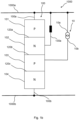
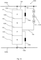
- Figures 1a-1e show several configurations of a current-controlled semiconductor system according to the disclosure, denoted with reference numeral 1000.
- the system 1000 comprises a signal line 1000a for carrying a signal as well as a ground line 1000b for connecting to an electrical ground.
- Current-controlled semiconductor system 1000 furthermore comprises a semiconductor controlled rectifier, SCR, device, denoted with 100, being electrically connected between both signal line 1000a and ground 1000b.
- SCR semiconductor controlled rectifier
- the semiconductor controlled rectifier, SCR, device 100 has an input SCR terminal 100a and an output SCR terminal 100b and is composed of a configuration, e.g. a stack, of four SCR layers.
- the first SCR layer 101 is doped with a first type of charge carriers, in this example P, and is electrically connected via the input SCR terminal 100a with the signal line 1000a.
- the first SCR layer 101 forms a first junction 120a with a second SCR layer 102, which is doped with a second type of charge carriers N different from the first type of charge carriers P.
- the semiconductor controlled rectifier, SCR, device 100 also comprises a third SCR layer 103, which doped with the first type of P-type charge carriers and the third SCR layer 103 forms a second junction 120b with the second SCR layer 102.
- a fourth SCR layer 104 doped with the second type of N-type charge carriers forms a third junction with the third SCR layer 103.
- the fourth SCR layer 104 is also electrically connected with the ground line 1000b by means of the output SCR terminal 100b.
- Reference numerals 130a and 130b denote first and second SCR junction elements.
- the first SCR junction element 130a electrically connects the second SCR layer 102 with the signal line 100a.
- the second SCR junction element 130b electrically connect the third SCR layer 103 with the ground line 100b.
- the first and second SCR junction elements 130a and 130b comprises a resistor.
- Figure 1a depicts the semiconductor controlled rectifier, SCR, device 100 with both the second and third SCR layers 102 and 103 being electrically connected via a first and a second SCR junction element 130a and 130b with the signal line 1000a and ground line 1000b, respectively.
- SCR semiconductor controlled rectifier
- the current-controlled semiconductor system 1000 furthermore comprises at least one current trigger device 10.
- the at least one current trigger device 10 electrically connects the signal line 1000a with the third SCR layer 103.
- the at least one current trigger device 10 has an input terminal 10a connected with the signal line 1000a and an output terminal 10b electrically connected with the third SCR layer 103.
- the at least one current trigger device 10 electrically connects the ground line 1000b with the second SCR layer 102.
- the at least one current trigger device 10 has an input terminal 10a connected with the second SCR layer 102 and an output terminal 10b electrically connected with the ground line 1000b.
- the at least one current trigger device 10 may be configured as a resistor triggered Shockley diode, RTS.
- RTS device 10 shows a leakage current similar to a stack of two forward diodes. However, at higher current levels, after the inherent thyristor has ignited, they behave like a single forward diode. Accordingly in this disclosure, the semiconductor controlled rectifier, SCR, device 100 being triggered with at least one current trigger device (or RTS) 10 will exhibit a low leakage current similar to a SCR triggered with a stack of two diodes and a low trigger voltage similar to a SCR triggered with one diode only.
- one RTS 10 or stacks of multiple RTSs, e.g. more than one RTS electrically connected in series as depicted in the configuration of Figure 1d
- both a low leakage and a low trigger can be achieved at the same time.
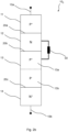
- FIG. 2a A first example of such current trigger device 10 is shown in Figures 2a , with additional examples shown in Figures 2b-2d and 3 , in a schematic view and in cross-sectional view.
- the first example (see Figure 2a ) of the semiconductor device according to the disclosure is denoted with reference numeral 10 1 , and comprises a first layer 11 which is doped with a first type of charge carriers, here P-type carriers.
- the first layer 11 forms a first junction 20a with a second layer 12, which is doped with a second type of N-type charge carriers, which are different from the first type of P charge carriers.
- a third layer 13 which doped with the first type of P-type charge carriers forms a second junction 20b with the second layer
- a fourth layer 14, which is doped with the second type of N-type charge carriers forms a third junction with the third layer.
- Each example depicted in this application also comprises an input terminal 10a, which is electrically connected with the signal line 100a and with the first layer 11 and an output terminal 10b, which is electrically connected with the fourth layer 14 and the third SCR layer 103.
- the first layer 11, its first junction 10a, the second 12, its second junction 10b, and the third layer 13 form a first bipolar junction transistor, BJT.
- the second layer 12, the second junction 10b, the third layer 13, the third junction 10c and the fourth layer 14 form a second bipolar junction transistor, BJT.
- reference numeral 30 denotes a junction element which electrically connects the second layer 12 with the third layer 13.
- the junction element 30 can be any metal functioning as an electric short between the second layer 12 with the third layer 13.
- the third layer 13 comprises a region 13a which adjoins the second layer 12, which region 13a has a high dopant concentration of charge carriers.
- the third layer 13 is doped with the first type of P-type charge carriers, and accordingly its high dopant concentration is denoted with the annotation P+.
- the electrical junction element 30 may function as a short between the two base contacts, formed by the second and third layers 12 and 13 respectively, of each BJT, see the example of Figure 4 . It reduces the trigger voltage to the equivalent of two forward biased diodes.
- both emitter-base junctions 20a and 20c, between the first-second layers 11-12 and fourth-third layers 13-14, are forward biased at the same time. Injection of minority carriers starts from both sides via the input and output terminals 10a-10b and the turn-on effect is fast.
- Figure 2b depicts a second configuration of the second example 10 2 of the disclosure, wherein the junction element 30 electrically connects the second layer 12 with the high dopant region 13a (P+) of the third layer 13.
- Figure 2c depicts a second configuration of the second example 10 2 of the disclosure, wherein the junction element 30 electrically connects the second layer 12 with the low dopant region 13b (P-) of the third layer 13.
- the electrical junction element 30 may function as a resistor between the two base contacts of each BJT (see Figures 2b and 2c ), or as a stack of diodes 30 1 ;..30 N connected in series, with N ⁇ 1, the latter configuration being depicted in Figure 2d and similarly electrically connecting the second layer 12 with either the high dopant region 13a (P+) or the low dopant region 13b (P-) of the third layer 13. Also a combination of a resistor and diodes connected in series is a feasible configuration.
- the emitter-base junction 20a has a low capacitance, therefore, the semiconductor controlled rectifier has a low capacitance, too.
- the third layer 13 has two dopant regions 13a and 13b.
- a low dopant region 13b adjoins the high dopant region 13a of the third layer 13, but as show in the Figures 4 and 5 , the low dopant region 13b also adjoins the fourth layer 14 having N-type charge carriers.
- the doping of the high dopant region 13a is higher than the doping of the low dopant region 13b.
- the third layer 13 has P-type charge carriers, both doping are denoted with P+ (for high) and P- (for low).
- the fourth layer 14, functioning as one emitter for the BJT is electrically connected with or placed in a low doped part 13b (P-) of its adjacent base/third layer 13, as shown in Figure 5 .
- This emitter-base junction 20c has a low capacitance, and consequentially the semiconductor controlled rectifier exhibits beneficially a low capacitance.
- the second layer 12 also has two dopant regions 12a and 12b.
- a high dopant region 12b adjoins the high dopant region 13a of the third layer 13, forming the second junction 20b.
- the low dopant region 12a adjoins the first layer 11.
- the doping of the high dopant region 12b is higher than the doping of the low dopant region 12a.
- the second layer 12 has N-type charge carriers, both doping are denoted with N+ (for high) and N- (for low).
- both emitters formed by the first layer 11 and the fourth layer 14 are positioned in low doped base areas 12a (N-) and 13b (P-), respectively, see Figure 5 .
- Both emitter-base junctions 20a and 20c exhibit a low capacitance, and due to the series connection of both low-capacitance emitter-base junctions, the total capacitance of the semiconductor device 10 2 is small too.
- the example of a semiconductor device 10 2 only implementing the third layer 13 with two dopant regions 13a (P+) and 13b (P-), and the example of a semiconductor device 10 2 implementing the third layer 13 with two dopant regions 13a (P+) and 13b (P-) as well as the second layer 12 with two dopant regions 12a (N-) and 12b (N+) are functional examples of the disclosure.
- junction element 30 electrically connects either dopant region 12a (N-) or 12b (N+) of the second layer 12 with either dopant region 13a (P+) or 13b (P-) of the third layer 13.
- the junction element 30 may interconnect dopant region 12a (N-) with either dopant region 13a (P+) or 13b (P-) or the junction element 30 may interconnect dopant region 12b (N+) with either dopant region 13a (P+) or 13b (P-).
- the fourth layer 14 may comprise a high dopant concentration denoted with N+.
- the fourth layer 14 is formed of a high dopant region 14b (N+) and a low dopant region 14a (N-), which functions as a depletion zone.
- the emitter-base junction (third junction 20c) thus formed also exhibits a low capacitance.
- the low doped region 13b (P-) is not necessarily part of the base layer 13. Comparable results are achievable with a low doped region 14a as depletion zone (N-) within the emitter/fourth layer 14.
- the high doping for both the P-type charge carriers as the N-type charge carriers used may include a high dopant region (P+ or N+) having a doping greater than 1 ⁇ 10 15 cm -3 and a layer thickness greater than 0.2 ⁇ m, more in particular a doping greater than 1 ⁇ 10 16 cm -3 and a layer thickness greater than 1 ⁇ m.
- the low dopant region (P- or N-) may have a doping smaller than 1 ⁇ 10 15 cm -3 and a layer thickness greater than 1 ⁇ m, more in particular a doping smaller than 1 ⁇ 10 14 cm -3 and a layer thickness greater than > 2 ⁇ m.
- the first layer 11 has a doping (P+) higher than the doping of the low dopant region 13b (P-) of the third layer 13.
- the fourth layer 14 is formed as a well (either as with dopant concentration N or high dopant concentration N+) in the low dopant region 13b (P-) of the third layer 13.
- the high dopant region 13a (P+) of the third layer 13 may be formed as a well in the low dopant region 13b (P-) of the third layer 13, see Figure 3 , 5 .
- the second layer 12 may be formed as a well in the high dopant region 13a (P+) of the third layer 13, see Figure 3 and 5 .
- the third layer 13 functions as a substrate (e.g. a P substrate) in the example 10 3 of Figure 3 .
- the high doped (P+) well 13a is placed within the P-substrate 13 with a proper distance between the well 13a and a N+-diffusion well 14 placed in the low dopant region 13b of the substrate 13.
- the N+-diffusion well 14 is in turn is connected with the output terminal 10b.
- a N-doped well 12 is placed within the P+-well 13a.
- the N-well 12 and the P+-well 13a are electrically contacted and connected to each other via the junction element 30, thus forming a short.
- the first layer 11 may be formed as a P+-diffusion well in the second layer 12 and connected with the input terminal 10a.
- such semiconductor device 10 4 can be manufactured in a logical sequence of manufacturing steps as shown in Figure 3 and 5 .
- This embodiments have additional advantages: the connection between the two bases 11 and 12 is local, and this facilitates the implementation for so-called multi-finger layouts.
- both emitters 11 and 14 can be placed in low doped base areas, denoted with N- regions 12a and P- regions13b.
- FIG. 6 another example 10 4 of a semiconductor device according to the disclosure is depicted.
- Reference numeral 50 denotes a buried oxide substrate implementing silicon-on-insulator, SOI, technology, and the buried oxide substrate 50 may be supported by a wafer carrier 60, e.g. made of silicon.
- the buried oxide substrate 50 is used as a base layer on which the third layer 13 is deposited.
- the third layer 13 is formed of a low dopant region (P-) 13b and an high dopant region (P+) 13a.
- the fourth layer 14 is formed in the low dopant region 13b, whereas the second layer 12 is formed as a well in the high dopant region 13a.
- the first layer 11 is formed as a well in the second layer 12.
- Junction element 30 shorts the second layer and the high dopant region 13a, and the first layer well 11 and the fourth layer well 14 form the input terminal 10a and output terminal 10b, respectively.
- the semiconductor device 10 4 of Figure 7 realizes the anti-punch-through with a deep P-well 13a and a buried P-well 13a of high dopant (P+) surrounding the N-well 14 (the fourth layer / emitter 14).
- the second layer 12 is formed as a well in the low dopant (13b / P-) third layer substrate 13.
- the first layer 11 is formed as a well in the second layer 12.
- the junction element 30 shorts the second layer 12 and the high dopant region 13a.
- Figure 8 shows an example 10 5 of an semiconductor device according to the disclosure the first by the use of buried oxide (SOI technology).
- This embodiment is an example for low capacitance realized at both emitter-base junctions
- Figure 9 shows a particular example, wherein the semiconductor device 10 6 is formed of the first layer 11, the second layer 12, the third layer 13 and the fourth layer 14 being configured in a layered stack.
- the first layer 11 functions as a base layer or base substrate on which subsequent layers 12, 13 and 14 are mounted (through deposition or through another layering technique).
- Reference numeral 40 denotes a trench, which is formed in the layered stack and extends from the top, fourth layer 14, through the third layer 13 and into at least the second layer 12.
- an electrically conductive layer 30 is coated against the side walls 40a of the trench 40, thus forming the junction element 30.
- the electrically conductive layer 30 functions as an electrical short between the second layer 12 and the third layer 13.
- Figure 10 depicts an example denoted with reference numeral 10 7 which can be considered as a vertical Shockley diode.
- the first layer 11 functions as a substrate (here as a P-substrate), on which substrate 11 the second layers 12 (denoted as BN layer) and 13 (denoted as the BP layer) are formed.
- the second layers 12 denoted as BN layer
- 13 deposition or other layering technique.
- DP 13 and DN 12 By means of deep N- and P-diffusions contacts (denoted with DP 13 and DN 12) are created which electrically contact the buried base diffusions (BN layer 12 and BP layer 13).
- the required second layer contact 12 and the third layer contact 13 is formed, which are subsequently short-circuited by means of the electric junction element 30.
- the fourth layer 14 is formed as a low dopant region 14a (N-).
- the first junction 20a e.g. formed by the P+-contact 11 and the N-well 12
- the current subsequently flows through the N-well 12 to the N-well contact (causing a resistive voltage drop), through the junction element 30 towards the P-well contact, from the P-well contact through the P-well 13a and through the P-substrate 13 (causing a resistive voltage drop) and eventually through the substrate N+-junction 20c towards the output terminal 20b (causing another forward voltage drop).
- the trigger voltage is the sum of all four voltage drops at the trigger current, typically in the range of 2 Volts.
- the current trigger device e.g. the resistor triggered Shockley diode, RTS
- RTS resistor triggered Shockley diode
Landscapes
- Semiconductor Integrated Circuits (AREA)
Abstract
Description
- The present disclosure relates to a data transmission system and in particular, although not exclusively, to a data transmission system with electrostatic discharge (ESD) or electrical overstress (EOS) protection.
- Electrostatic discharge is a problem encountered in a range of electronic systems, including data transmission systems. When an ESD event occurs in a data transmission system, components of the data transmission system may be damaged if the discharge is not suitably dissipated by the system.
- Semiconductor controlled rectifiers or SCRs are popular for ESD protection due to their deep snap-back and consequently low clamping voltage. The trigger voltages can be high, especially when a low capacitance is needed for proper operation. For reducing the trigger voltage, a well-known solution implements external triggering, that is using a current source with a low turn-on voltage to forward bias one emitter base junction of the SCR. For very low trigger voltages diode strings can be used for creating the necessary trigger current.
- A problem when implementing diode strings for external triggering is that such diode strings have no clear breakdown. Instead they show an exponential dependence of the current with a slope of N*60mV/decade. A typical string of N diodes will have 1nA leakage at N*250mV, whereas a trigger current of e.g. 10mA will only be reached at N*(250+7*60mV) = N*670mV. Accordingly, the difference between the low-leakage voltage range and the trigger voltage will be large.
- Thus, it is a goal of the present disclosure to provide an improved data transmission system obviating the above sketched issues.
- According to a first example of the disclosure, a current-controlled semiconductor system is proposed, which comprises a signal line for carrying a signal; a ground line for connecting to ground; and a semiconductor controlled rectifier, SCR, device. According to the disclosure, the semiconductor controlled rectifier, SCR, device consists of a first SCR layer doped with a first type of charge carriers; a second SCR layer doped with a second type of charge carriers different from the first type of charge carriers; a third SCR layer doped with the first type of charge carriers; a fourth SCR layer doped with the second type of charge carriers; an input terminal electrically connected with the first SCR layer and the signal line as well as an output terminal electrically connected with the fourth SCR layer and the ground line. Furthermore, at least a first SCR junction element is provided, electrically connected with the second SCR layer and the signal line, and/or a second SCR junction element is provided, electrically connected with the third SCR layer and the ground line.
- According to the disclosure the current-controlled semiconductor system furthermore comprises at least one current trigger device electrically connecting the signal line with the third SCR layer or the ground line with second SCR layer, the at least one current trigger device comprising a first layer doped with a first type of charge carriers; a second layer doped with a second type of charge carriers different from the first type of charge carriers; a third layer doped with the first type of charge carriers; a fourth layer doped with the second type of charge carriers; and an input terminal electrically connected with the first layer and the signal line and an output terminal electrically connected with the fourth layer and the third SCR layer, and a junction element which electrically connects the second layer and the third layer of the current trigger device.
- The at least one current trigger device which may be configured as a resistor triggered Shockley diode, RTS, show a leakage current similar to a stack of two forward diodes. However, at higher current levels, after the inherent thyristor has ignited, they behave like a single forward diode. Accordingly, the semiconductor controlled rectifier, SCR, device being triggered with at least one current trigger device (or RTS) will exhibit a low leakage current similar to a SCR triggered with a stack of two diodes and a low trigger voltage similar to a SCR triggered with one diode only. Thus, when implementing one RTS (or stacks of multiple RTSs, e.g. more than one RTS) to trigger a SCR device, both a low leakage and a low trigger can be achieved at the same time.
- The first, second and third layer in the at least one current trigger device form a first bipolar junction transistor, BJT, and the second, third and fourth layer form a second bipolar junction transistor, BJT. Additionally, in the at least one current trigger device, a junction element is provided which electrically connects the second layer with the third layer. Furthermore, the third layer comprises a high dopant region adjoining the second layer.
- The electrical junction element functions as a short between the two base contacts of each BJT. It reduces the trigger voltage to the equivalent of two forward biased diodes. When the device gets triggered, both emitter base junctions, between the first-second layer and fourth-third layer, are forward biased at the same time. Injection of minority carriers starts from both sides and the turn-on effect is fast. At least one of the emitter base junctions has a low capacitance, therefore, the semiconductor controlled rectifier has a low capacitance, too.
- In a preferred example of the current-controlled semiconductor system, in the at least one current trigger device, the third layer comprises a high dopant region adjoining the second layer.
- In a further example of the current-controlled semiconductor system, in the at least one current trigger device, the third layer comprises a low dopant region adjoining the high dopant region of the third layer as well as adjoining the fourth layer. It is noted that in this example, the doping of the high dopant region is higher than the doping of the low dopant region. Accordingly, as one emitter, formed by the fourth layer, is connected with or placed in a low doped part of its adjacent base, and therefore, this emitter-base junction has a low capacitance, and consequentially the semiconductor controlled rectifier exhibits beneficially a low capacitance. This obviated the use of an additional trigger diode. Therefore, sophisticated isolation schemes to inhibit the parasitic interactions between the external trigger diode and the semiconductor controlled rectifier are not needed, resulting in a simplified, yet effective configuration.
- In a further advantageous example, in the at least one current trigger device, the second layer comprises a high dopant region adjoining the high dopant region of the third layer and a low dopant region adjoining the first layer, wherein the doping of the high dopant region is higher than the doping of the low dopant region. With this example, both emitters (formed by the first and fourth layers) are positioned in low doped base areas. Both emitter-base junctions exhibit a low capacitance, and due to the series connection of both low-capacitance emitter-base junctions, the total capacitance of the semiconductor device is small too.
- In yet another beneficial example of the current-controlled semiconductor system according to the disclosure, in the at least one current trigger device, the fourth layer comprises a high dopant region adjoining the output terminal and a low dopant region adjoining the third layer, wherein the doping of the high dopant region is higher than the doping of the low dopant region. Likewise, the emitter-base junction thus formed also exhibits a low capacitance
- It should be noted, that for both the semiconductor controlled rectifier, SCR, device and the at least one current trigger device, that the first type of charge carriers may be P-type carriers, whereas the second type of charge carriers may be N-type carriers. However, the reversed configuration, wherein the first type of charge carriers are N-type carriers and the second type of charge carriers are P-type carriers is equally appliable in achieving the desired effect of creating one of both of the emitter base junctions having a low capacitance.
- Beneficial examples as to the high doping used may include a high dopant region having a doping greater than 1×1015 cm-3 and a layer thickness greater than 0.2 µm, more in particular a doping greater than 1×1016 cm-3 and a layer thickness greater than 1 µm. Likewise, as to the low doping, the low dopant region may have a doping smaller than 1×1015 cm-3 and a layer thickness greater than 1 µm, more in particular a doping smaller than 1×1014 cm-3 and a layer thickness greater than > 2 µm.
- Preferably, the first layer has a doping higher than the doping of the low dopant region of the third layer.
- In advantageous examples of the current-controlled semiconductor system according to the disclosure, in the at least one current trigger device, the fourth layer is formed as a well in the low dopant region of the third layer. Likewise, the high dopant region of the third layer may be formed as a well in the low dopant region of the third layer. And the second layer may be formed as a well in the high dopant region of the third layer, whereas the first layer is formed as a well in the second layer. Accordingly, such semiconductor device can be manufactured in a logical sequence of manufacturing steps.
- In a preferred example of the current-controlled semiconductor system according to the disclosure, in the at least one current trigger device, the first, second, third and fourth layer are configured in a layered stack. More in particular, a trench is formed in the layered stack extending from/through the fourth layer into at least the second layer, and the junction element is configured as an electrically conductive layer coating the trench. In this configuration the electrically conductive layer functions as an electrical short between the second and the third layer.
- Alternatively, an oxide substrate may be used on which the third layer is deposited.
- The disclosure will now be discussed with reference to the drawings, which show in:
-
Figure 1a-1e schematic several configurations of a current-controlled semiconductor system according to the disclosure; -
Figure 2a-2d schematic several configurations of a first and second example of a current-controlled semiconductor system according to the disclosure; -
Figure 3 another view of the second example as depicted inFigure 2b-2d ; -
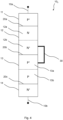
Figure 4 schematic a third example of the disclosure; -
Figure 5 another view of the third example of the disclosure as depicted inFigure 4 ; -
Figure 6 a fourth example of the disclosure;6 -
Figure 7 another view of the fourth example of the disclosure; -
Figure 8 a fifth example of the disclosure; -
Figure 9 a sixth example of the disclosure; -
Figure 10 a seventh example of the disclosure; -
Figures 11a 11b another views of the seventh example of the disclosure; -
Figure 12 a graph outlining the operation of several configurations and examples of the current-controlled semiconductor system according to the disclosure. - For a proper understanding of the disclosure, in the detailed description below corresponding elements or parts of the disclosure will be denoted with identical reference numerals in the drawings.
- For the sake of clarity, it is noted that in this application several examples of semiconductor devices according to the disclosure are depicted, whose configuration is formed of layers, which are doped with a first type of charge carriers or with a second type of charge carriers, wherein the second type of charge carriers are different from the first type of charge carriers.
- Throughout the following detailed description it is understood, that the first type of charge carriers are P-type carriers, and the second type of charge carriers are logically N-type carriers. However, the reversed configuration, wherein the first type of charge carriers are N-type carriers and the second type of charge carriers are P-type carriers is equally appliable in all examples described in this application, as both configurations (PN or NP) achieve the desired effect of creating one or both of the emitter base junctions of having a low capacitance.
-
Figures 1a-1e show several configurations of a current-controlled semiconductor system according to the disclosure, denoted withreference numeral 1000. Thesystem 1000 comprises asignal line 1000a for carrying a signal as well as aground line 1000b for connecting to an electrical ground. Current-controlledsemiconductor system 1000 furthermore comprises a semiconductor controlled rectifier, SCR, device, denoted with 100, being electrically connected between bothsignal line 1000a andground 1000b. - The semiconductor controlled rectifier, SCR,
device 100 has aninput SCR terminal 100a and anoutput SCR terminal 100b and is composed of a configuration, e.g. a stack, of four SCR layers. Thefirst SCR layer 101 is doped with a first type of charge carriers, in this example P, and is electrically connected via theinput SCR terminal 100a with thesignal line 1000a. Thefirst SCR layer 101 forms afirst junction 120a with asecond SCR layer 102, which is doped with a second type of charge carriers N different from the first type of charge carriers P. - The semiconductor controlled rectifier, SCR,
device 100 also comprises athird SCR layer 103, which doped with the first type of P-type charge carriers and thethird SCR layer 103 forms asecond junction 120b with thesecond SCR layer 102. Afourth SCR layer 104 doped with the second type of N-type charge carriers forms a third junction with thethird SCR layer 103. Thefourth SCR layer 104 is also electrically connected with theground line 1000b by means of theoutput SCR terminal 100b. -
Reference numerals SCR junction element 130a electrically connects thesecond SCR layer 102 with thesignal line 100a. Likewise, the secondSCR junction element 130b electrically connect thethird SCR layer 103 with theground line 100b. - In all configurations, the first and second
SCR junction elements - The configuration of
Figure 1a depicts the semiconductor controlled rectifier, SCR,device 100 with both the second and third SCR layers 102 and 103 being electrically connected via a first and a secondSCR junction element signal line 1000a andground line 1000b, respectively. However, also configurations with only one SCR junction element are feasible, such as thesecond SCR layer 102 being electrically connected via the firstSCR junction element 130a with thesignal line 1000a (Figure 1b ) or thethird SCR layer 103 being electrically connected via the secondSCR junction element 130b with theground line 1000b (Figure 1c ). - Additionally, in all configurations of the current-controlled
semiconductor system 1000 shown, it furthermore comprises at least onecurrent trigger device 10. In the example ofFigures 1a-1d , the at least onecurrent trigger device 10 electrically connects thesignal line 1000a with thethird SCR layer 103. The at least onecurrent trigger device 10 has aninput terminal 10a connected with thesignal line 1000a and anoutput terminal 10b electrically connected with thethird SCR layer 103. - Alternatively, as shown in the example of
Figure 1e , the at least onecurrent trigger device 10 electrically connects theground line 1000b with thesecond SCR layer 102. Likewise, the at least onecurrent trigger device 10 has aninput terminal 10a connected with thesecond SCR layer 102 and anoutput terminal 10b electrically connected with theground line 1000b. - In the below detailed description, all configurations and examples depict the at least one
current trigger device 10 being electrically connecting thesignal line 1000a with thethird SCR layer 103, as shown inFigure 1a . However, it should be note that all configurations and examples depicted can likewise be implemented with the at least onecurrent trigger device 10 electrically connecting theground line 1000b with thesecond SCR layer 102, as shown inFigure 1e , for example combined with either example of the configurations of the first and secondSCR junction elements 130a-130b ofFigures 1b-1d . - The at least one
current trigger device 10 may be configured as a resistor triggered Shockley diode, RTS.Such RTS device 10 shows a leakage current similar to a stack of two forward diodes. However, at higher current levels, after the inherent thyristor has ignited, they behave like a single forward diode. Accordingly in this disclosure, the semiconductor controlled rectifier, SCR,device 100 being triggered with at least one current trigger device (or RTS) 10 will exhibit a low leakage current similar to a SCR triggered with a stack of two diodes and a low trigger voltage similar to a SCR triggered with one diode only. Thus, when implementing one RTS 10 (or stacks of multiple RTSs, e.g. more than one RTS electrically connected in series as depicted in the configuration ofFigure 1d ) to trigger aSCR device 100, both a low leakage and a low trigger can be achieved at the same time. - A first example of such
current trigger device 10 is shown inFigures 2a , with additional examples shown inFigures 2b-2d and3 , in a schematic view and in cross-sectional view. The first example (seeFigure 2a ) of the semiconductor device according to the disclosure is denoted withreference numeral 101, and comprises afirst layer 11 which is doped with a first type of charge carriers, here P-type carriers. Thefirst layer 11 forms afirst junction 20a with asecond layer 12, which is doped with a second type of N-type charge carriers, which are different from the first type of P charge carriers. - Also, a
third layer 13 which doped with the first type of P-type charge carriers forms asecond junction 20b with the second layer, and afourth layer 14, which is doped with the second type of N-type charge carriers forms a third junction with the third layer. - Each example depicted in this application also comprises an
input terminal 10a, which is electrically connected with thesignal line 100a and with thefirst layer 11 and anoutput terminal 10b, which is electrically connected with thefourth layer 14 and thethird SCR layer 103. - The
first layer 11, itsfirst junction 10a, the second 12, itssecond junction 10b, and thethird layer 13 form a first bipolar junction transistor, BJT. Similarly, thesecond layer 12, thesecond junction 10b, thethird layer 13, the third junction 10c and thefourth layer 14 form a second bipolar junction transistor, BJT. - Also,
reference numeral 30 denotes a junction element which electrically connects thesecond layer 12 with thethird layer 13. Thejunction element 30 can be any metal functioning as an electric short between thesecond layer 12 with thethird layer 13. - As depicted in the second example 102 as shown in
Figures 2b-1d and3 , thethird layer 13 comprises aregion 13a which adjoins thesecond layer 12, whichregion 13a has a high dopant concentration of charge carriers. In the examples shown, thethird layer 13 is doped with the first type of P-type charge carriers, and accordingly its high dopant concentration is denoted with the annotation P+. - The
electrical junction element 30 may function as a short between the two base contacts, formed by the second andthird layers Figure 4 . It reduces the trigger voltage to the equivalent of two forward biased diodes. When thedevice 102 gets triggered, both emitter-base junctions output terminals 10a-10b and the turn-on effect is fast. -
Figure 2b depicts a second configuration of the second example 102 of the disclosure, wherein thejunction element 30 electrically connects thesecond layer 12 with thehigh dopant region 13a (P+) of thethird layer 13.Figure 2c depicts a second configuration of the second example 102 of the disclosure, wherein thejunction element 30 electrically connects thesecond layer 12 with thelow dopant region 13b (P-) of thethird layer 13. - Additionally, the
electrical junction element 30 may function as a resistor between the two base contacts of each BJT (seeFigures 2b and2c ), or as a stack ofdiodes 301;..30N connected in series, with N≥1, the latter configuration being depicted inFigure 2d and similarly electrically connecting thesecond layer 12 with either thehigh dopant region 13a (P+) or thelow dopant region 13b (P-) of thethird layer 13. Also a combination of a resistor and diodes connected in series is a feasible configuration. - In the example of
Figures 2b-2d and3 , the emitter-base junction 20a has a low capacitance, therefore, the semiconductor controlled rectifier has a low capacitance, too. - In the example of
Figures 4 and5 , thethird layer 13 has twodopant regions low dopant region 13b adjoins thehigh dopant region 13a of thethird layer 13, but as show in theFigures 4 and5 , thelow dopant region 13b also adjoins thefourth layer 14 having N-type charge carriers. The doping of thehigh dopant region 13a is higher than the doping of thelow dopant region 13b. As in these examples, thethird layer 13 has P-type charge carriers, both doping are denoted with P+ (for high) and P- (for low). - Thus, the
fourth layer 14, functioning as one emitter for the BJT, is electrically connected with or placed in a lowdoped part 13b (P-) of its adjacent base/third layer 13, as shown inFigure 5 . This emitter-base junction 20c has a low capacitance, and consequentially the semiconductor controlled rectifier exhibits beneficially a low capacitance. This obviated the use of an additional trigger diode. Therefore, sophisticated isolation schemes to inhibit the parasitic interactions between the external trigger diode and the semiconductor controlled rectifier are not needed, resulting in a simplified, yet effective configuration. - In a further advantageous example, which is also depicted in
Figure 4 andFigure 5 , thesecond layer 12 also has twodopant regions high dopant region 12b adjoins thehigh dopant region 13a of thethird layer 13, forming thesecond junction 20b. Thelow dopant region 12a adjoins thefirst layer 11. Likewise it is to be noted, that the doping of thehigh dopant region 12b is higher than the doping of thelow dopant region 12a. As in these examples, thesecond layer 12 has N-type charge carriers, both doping are denoted with N+ (for high) and N- (for low). - Here, both emitters formed by the
first layer 11 and thefourth layer 14 are positioned in low dopedbase areas 12a (N-) and 13b (P-), respectively, seeFigure 5 . Both emitter-base junctions semiconductor device 102 is small too. - Note that the example of a
semiconductor device 102 only implementing thethird layer 13 with twodopant regions 13a (P+) and 13b (P-), and the example of asemiconductor device 102 implementing thethird layer 13 with twodopant regions 13a (P+) and 13b (P-) as well as thesecond layer 12 with twodopant regions 12a (N-) and 12b (N+) are functional examples of the disclosure. - Likewise, several configurations are possible, wherein the
junction element 30 electrically connects eitherdopant region 12a (N-) or 12b (N+) of thesecond layer 12 with eitherdopant region 13a (P+) or 13b (P-) of thethird layer 13. Thus, thejunction element 30 may interconnectdopant region 12a (N-) with eitherdopant region 13a (P+) or 13b (P-) or thejunction element 30 may interconnectdopant region 12b (N+) with eitherdopant region 13a (P+) or 13b (P-). - Optionally, as shown for example in
Figures 2b-2d ,4 and5 (and optionally also in the examples ofFigures 11a-11b ), thefourth layer 14 may comprise a high dopant concentration denoted with N+. Alternatively, in an advantageous example (seeFigure 10 and11a-11b ), thefourth layer 14 is formed of ahigh dopant region 14b (N+) and alow dopant region 14a (N-), which functions as a depletion zone. Thehigh dopant region 14b (N+) adjoins theoutput terminal 10b and thelow dopant region 14a adjoins thethird layer 13, in an example thelow dopant region 14a (N-) adjoins thethird layer 13 having a high dopant concentration P+ (seeFigure 11a and11b ). Also in this example, the doping of thehigh dopant region 14b (N+) is higher than the doping of thelow dopant region 14a (N-). The emitter-base junction (third junction 20c) thus formed also exhibits a low capacitance. The lowdoped region 13b (P-) is not necessarily part of thebase layer 13. Comparable results are achievable with a lowdoped region 14a as depletion zone (N-) within the emitter/fourth layer 14. - The high doping for both the P-type charge carriers as the N-type charge carriers used may include a high dopant region (P+ or N+) having a doping greater than 1×1015 cm-3 and a layer thickness greater than 0.2 µm, more in particular a doping greater than 1×1016 cm-3 and a layer thickness greater than 1 µm. Likewise, as to the low doping for both P-type / N-type charge carriers, the low dopant region (P- or N-) may have a doping smaller than 1×1015 cm-3 and a layer thickness greater than 1 µm, more in particular a doping smaller than 1×1014 cm-3 and a layer thickness greater than > 2 µm.
- In a preferred example, the
first layer 11 has a doping (P+) higher than the doping of thelow dopant region 13b (P-) of thethird layer 13. - Further advantageous examples of the semiconductor device are shown in
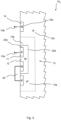
Figures 3 ,5-8 and10 . In an example, see e.g.Figure 3 ,5-10 and11b , thefourth layer 14 is formed as a well (either as with dopant concentration N or high dopant concentration N+) in thelow dopant region 13b (P-) of thethird layer 13. Likewise, thehigh dopant region 13a (P+) of thethird layer 13 may be formed as a well in thelow dopant region 13b (P-) of thethird layer 13, seeFigure 3 ,5 . And thesecond layer 12 may be formed as a well in thehigh dopant region 13a (P+) of thethird layer 13, seeFigure 3 and5 . - The
third layer 13 functions as a substrate (e.g. a P substrate) in the example 103 ofFigure 3 . The high doped (P+) well 13a is placed within the P-substrate 13 with a proper distance between the well 13a and a N+-diffusion well 14 placed in thelow dopant region 13b of thesubstrate 13. The N+-diffusion well 14 is in turn is connected with theoutput terminal 10b. A N-dopedwell 12 is placed within the P+-well 13a. The N-well 12 and the P+-well 13a are electrically contacted and connected to each other via thejunction element 30, thus forming a short. Likewise, thefirst layer 11 may be formed as a P+-diffusion well in thesecond layer 12 and connected with theinput terminal 10a. - Accordingly,
such semiconductor device 104 can be manufactured in a logical sequence of manufacturing steps as shown inFigure 3 and5 . This embodiments have additional advantages: the connection between the twobases Figure 5 , bothemitters regions 12a and P- regions13b. - In
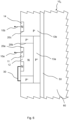
Figure 6 , another example 104 of a semiconductor device according to the disclosure is depicted.Reference numeral 50 denotes a buried oxide substrate implementing silicon-on-insulator, SOI, technology, and the buriedoxide substrate 50 may be supported by awafer carrier 60, e.g. made of silicon. The buriedoxide substrate 50 is used as a base layer on which thethird layer 13 is deposited. Thethird layer 13 is formed of a low dopant region (P-) 13b and an high dopant region (P+) 13a. thefourth layer 14 is formed in thelow dopant region 13b, whereas thesecond layer 12 is formed as a well in thehigh dopant region 13a. Thefirst layer 11 is formed as a well in thesecond layer 12.Junction element 30 shorts the second layer and thehigh dopant region 13a, and the first layer well 11 and the fourth layer well 14 form theinput terminal 10a andoutput terminal 10b, respectively. - The
semiconductor device 104 ofFigure 7 realizes the anti-punch-through with a deep P-well 13a and a buried P-well 13a of high dopant (P+) surrounding the N-well 14 (the fourth layer / emitter 14). Thesecond layer 12 is formed as a well in the low dopant (13b / P-)third layer substrate 13. Thefirst layer 11 is formed as a well in thesecond layer 12. Also here, thejunction element 30 shorts thesecond layer 12 and thehigh dopant region 13a. -
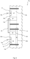
Figure 8 shows an example 105 of an semiconductor device according to the disclosure the first by the use of buried oxide (SOI technology). This embodiment is an example for low capacitance realized at both emitter-base junctions -
Figure 9 shows a particular example, wherein thesemiconductor device 106 is formed of thefirst layer 11, thesecond layer 12, thethird layer 13 and thefourth layer 14 being configured in a layered stack. In this example, thefirst layer 11 functions as a base layer or base substrate on whichsubsequent layers Reference numeral 40 denotes a trench, which is formed in the layered stack and extends from the top,fourth layer 14, through thethird layer 13 and into at least thesecond layer 12. Through a deposition or layering technique an electricallyconductive layer 30 is coated against theside walls 40a of thetrench 40, thus forming thejunction element 30. In this configuration the electricallyconductive layer 30 functions as an electrical short between thesecond layer 12 and thethird layer 13. -
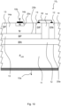
Figure 10 depicts an example denoted withreference numeral 107 which can be considered as a vertical Shockley diode. Also in this example, thefirst layer 11 functions as a substrate (here as a P-substrate), on whichsubstrate 11 the second layers 12 (denoted as BN layer) and 13 (denoted as the BP layer) are formed. On theBL layer 13 afourth layer 14 is formed, through deposition or other layering technique. By means of deep N- and P-diffusions contacts (denoted withDP 13 and DN 12) are created which electrically contact the buried base diffusions (BN layer 12 and BP layer 13). Accordingly the requiredsecond layer contact 12 and thethird layer contact 13 is formed, which are subsequently short-circuited by means of theelectric junction element 30. Note that in this example ofFigure 10 , thefourth layer 14 is formed as alow dopant region 14a (N-). - In all examples shown, when a positive voltage is applied at the
input terminal 10a connected with the first layer (e.g. the P+ contact), a current will flow through thefirst junction 20a (e.g. formed by the P+-contact 11 and the N-well 12) causing one forward voltage drop). The current subsequently flows through the N-well 12 to the N-well contact (causing a resistive voltage drop), through thejunction element 30 towards the P-well contact, from the P-well contact through the P-well 13a and through the P-substrate 13 (causing a resistive voltage drop) and eventually through the substrate N+-junction 20c towards theoutput terminal 20b (causing another forward voltage drop). - When the current exceeds a certain limit (trigger current) then the SCR will switch to its on-state and the current will flow directly from the N+-
contact 14 to the P+-contact 11. The trigger voltage is the sum of all four voltage drops at the trigger current, typically in the range of 2 Volts. - In all configurations as depicted in the accompanying Figures, the current trigger device (e.g. the resistor triggered Shockley diode, RTS) may operate, at low currents, below the trigger point, as a stack of two forward diodes. At a higher current, above the trigger point, the inherent thyristor is active and the current flows directly from one emitter to the other emitter and the forward voltage is similar to that of one forward biased diode. See Figure 19.
-
- 1000
- current-controlled semiconductor system (according to the disclosure)
- 1000a
- signal line
- 1000b
- ground line
- 100
- semiconductor controlled rectifier, SCR, device
- 100a
- input SCR terminal
- 100b
- output SCR terminal
- 101
- first SCR layer
- 102
- second SCR layer
- 103
- third SCR layer
- 104
- fourth SCR layer
- 120a/b/c
- first, second and third SCR junction interface
- 130a
- first SCR junction element
- 130b
- second SCR junction element
- 101-107
- current trigger device (1st - 7th example of the disclosure)
- 10-1..10-N
- stack of current trigger devices
- 10a
- first (emitter) terminal
- 10b
- second (emitter) terminal
- 11
- first layer doped
- 12
- second layer
- 12a
- low dopant region of second layer
- 12b
- high dopant region of second layer
- 13
- third layer
- 13a
- high dopant region of third layer
- 13b
- low dopant region of third layer
- 14
- fourth layer
- 14a
- low dopant region of fourth layer
- 14b
- high dopant region of fourth layer
- 20a-20c
- first, second and third junction interface
- 30
- junction element / short / resistor / trench layer coating
- 301..30N
- stack of junction elements / resistors / diodes (in series)
- 40
- trench
- 40a
- side wall of trench
- 50
- oxide substrate
- 60
- carrier wafer
Claims (15)
- A current-controlled semiconductor system comprising:a signal line for carrying a signal;a ground line for connecting to ground; anda semiconductor controlled rectifier, SCR, device comprising:a first SCR layer doped with a first type of charge carriers;a second SCR layer doped with a second type of charge carriers different from the first type of charge carriers;a third SCR layer doped with the first type of charge carriers;a fourth SCR layer doped with the second type of charge carriers;an input terminal electrically connected with the first SCR layer and the signal line as well as an output terminal electrically connected with the fourth SCR layer and the ground line;at least a first SCR junction element electrically connected with the second SCR layer and the signal line, and/or a second SCR junction element electrically connected with the third SCR layer and the ground line,the current-controlled semiconductor system further comprising at least one current trigger device electrically connecting the signal line with the third SCR layer or the ground line with second SCR layer, the at least one current trigger device comprising a first layer doped with a first type of charge carriers; a second layer doped with a second type of charge carriers different from the first type of charge carriers; a third layer doped with the first type of charge carriers; a fourth layer doped with the second type of charge carriers; and an input terminal electrically connected with the first layer and the signal line and an output terminal electrically connected with the fourth layer and the third SCR layer, and a junction element which electrically connects the second layer and the third layer of the current trigger device.
- The current-controlled semiconductor system according to claim 1, wherein, in the at least one current trigger device, the third layer comprises a high dopant region adjoining the second layer.
- The current-controlled semiconductor system according to claim 1 or 2, wherein, in the at least one current trigger device, the third layer comprises a low dopant region adjoining the high dopant region of the third layer as well as adjoining the fourth layer, wherein the doping of the high dopant region is higher than the doping of the low dopant region.
- The current-controlled semiconductor system according to any one more of the claims 1-3, wherein, in the at least one current trigger device, the second layer comprises a high dopant region adjoining the high dopant region of the third layer and a low dopant region adjoining the first layer, wherein the doping of the high dopant region is higher than the doping of the low dopant region.
- The current-controlled semiconductor system according to any one or more of the preceding claims, wherein the fourth layer comprises a high dopant region adjoining the output terminal and a low dopant region adjoining the third layer, wherein the doping of the high dopant region is higher than the doping of the low dopant region.
- The current-controlled semiconductor system according to any one or more of the claims 1-5, wherein the first type of charge carriers are P-type carriers and the second type of charge carriers are N-type carriers.
- The current-controlled semiconductor system according to any one or more of the claims 1-5, wherein the first type of charge carriers are N-type carriers and the second type of charge carriers are P-type carriers.
- The current-controlled semiconductor system according to any one or more of the preceding claims, wherein the high dopant region has a doping greater than 1×1015 cm-3 and a layer thickness greater than 0.2 µm, more in particular a doping greater than 1×1016 cm-3 and a layer thickness greater than 1 µm.
- The current-controlled semiconductor system according to any one or more of the preceding claims, wherein the low dopant region has a doping smaller than 1×1015 cm-3 and a layer thickness greater than 1 µm, more in particular a doping smaller than 1×1014 cm-3 and a layer thickness greater than > 2 µm.
- The current-controlled semiconductor system according to any one or more of the preceding claims, wherein, in the at least one current trigger device, the fourth layer is formed as a well in the low dopant region of the third layer.
- The current-controlled semiconductor system according to any one or more of the preceding claims, wherein, in the at least one current trigger device, the high dopant region of the third layer is formed as a well in the low dopant region of the third layer.
- The current-controlled semiconductor system according to any one or more of the preceding claims, wherein, in the at least one current trigger device, the second layer is formed as a well in the high dopant region of the third layer.
- The current-controlled semiconductor system according to any one or more of the preceding claims, wherein, in the at least one current trigger device, the first layer is formed as a well in the second layer.
- The current-controlled semiconductor system according to any one or more of the preceding claims, wherein, in the at least one current trigger device, the first layer has a doping higher than the doping the low dopant region of the third layer.
- The current-controlled semiconductor system according to any one or more of the preceding claims, wherein, in the at least one current trigger device, the first, second, third and fourth layer are configured in a layered stack and wherein a trench is formed in the layered stack from the fourth layer into at least the second layer, and wherein the junction element is configured as an electrically conductive layer coating the trench.
Priority Applications (3)
| Application Number | Priority Date | Filing Date | Title |
|---|---|---|---|
| EP22209615.8A EP4376078A1 (en) | 2022-11-25 | 2022-11-25 | A data transmission system |
| US18/516,376 US20240178659A1 (en) | 2022-11-25 | 2023-11-21 | Data transmission system |
| CN202311578181.1A CN118099155A (en) | 2022-11-25 | 2023-11-24 | Data transmission system |
Applications Claiming Priority (1)
| Application Number | Priority Date | Filing Date | Title |
|---|---|---|---|
| EP22209615.8A EP4376078A1 (en) | 2022-11-25 | 2022-11-25 | A data transmission system |
Publications (1)
| Publication Number | Publication Date |
|---|---|
| EP4376078A1 true EP4376078A1 (en) | 2024-05-29 |
Family
ID=84362955
Family Applications (1)
| Application Number | Title | Priority Date | Filing Date |
|---|---|---|---|
| EP22209615.8A Pending EP4376078A1 (en) | 2022-11-25 | 2022-11-25 | A data transmission system |
Country Status (3)
| Country | Link |
|---|---|
| US (1) | US20240178659A1 (en) |
| EP (1) | EP4376078A1 (en) |
| CN (1) | CN118099155A (en) |
Citations (4)
| Publication number | Priority date | Publication date | Assignee | Title |
|---|---|---|---|---|
| US7471493B1 (en) * | 2002-11-14 | 2008-12-30 | Altera Corporation | Fast and compact SCR ESD protection device for high-speed pins |
| US20180219006A1 (en) * | 2017-02-02 | 2018-08-02 | Globalfoundries Inc. | Diode-triggered schottky silicon-controlled rectifier for fin-fet electrostatic discharge control |
| US20200091138A1 (en) * | 2018-05-17 | 2020-03-19 | Jiangnan University | Esd protection device with bidirectional diode string-triggering scr structure |
| US20200303369A1 (en) * | 2019-03-20 | 2020-09-24 | Semiconductor Manufacturing International (Shanghai) Corporation | Silicon-controlled-rectifier electrostatic protection structure and fabrication method thereof |
Family Cites Families (13)
| Publication number | Priority date | Publication date | Assignee | Title |
|---|---|---|---|---|
| US5671111A (en) * | 1995-10-30 | 1997-09-23 | Motorola, Inc. | Apparatus for electro-static discharge protection in a semiconductor device |
| US5734541A (en) * | 1996-05-20 | 1998-03-31 | Pmc-Sierra, Inc. | Low voltage silicon controlled rectifier structure for ESD input pad protection in CMOS IC's |
| US6873505B2 (en) * | 1999-09-14 | 2005-03-29 | United Microelectronics Corp. | Electrostatic discharge protective circuitry equipped with a common discharge line |
| US20080002321A1 (en) * | 2006-06-29 | 2008-01-03 | Bart Sorgeloos | Electrostatic discharge protection of a clamp |
| US7663190B2 (en) * | 2007-10-08 | 2010-02-16 | Intersil Americas Inc. | Tunable voltage isolation ground to ground ESD clamp |
| CN101938119B (en) * | 2009-06-30 | 2014-01-15 | 万国半导体股份有限公司 | Transient voltage suppressor (TVS) with improved clamping voltage |
| US8243404B2 (en) * | 2009-08-18 | 2012-08-14 | Faraday Technology Corp. | ESD protection circuit with merged triggering mechanism |
| US8248741B2 (en) * | 2009-09-16 | 2012-08-21 | Integrated Device Technology, Inc. | Apparatuses and methods for a SCR-based clamped electrostatic discharge protection device |
| US8634172B2 (en) * | 2010-05-18 | 2014-01-21 | International Business Machines Corporation | Silicon controlled rectifier based electrostatic discharge protection circuit with integrated JFETs, method of operation and design structure |
| WO2012119788A1 (en) * | 2011-03-10 | 2012-09-13 | Qpx Gmbh | Integrated circuit including silicon controlled rectifier |
| US8611058B2 (en) * | 2011-08-23 | 2013-12-17 | Micron Technology, Inc. | Combination ESD protection circuits and methods |
| CN208045498U (en) * | 2017-03-29 | 2018-11-02 | 意法半导体国际有限公司 | Circuit for providing static discharge (ESD) protection |
| US11721974B2 (en) * | 2021-01-04 | 2023-08-08 | Changxin Memory Technologies, Inc. | Electrostatic discharge (ESD) protection circuit and chip |
-
2022
- 2022-11-25 EP EP22209615.8A patent/EP4376078A1/en active Pending
-
2023
- 2023-11-21 US US18/516,376 patent/US20240178659A1/en active Pending
- 2023-11-24 CN CN202311578181.1A patent/CN118099155A/en active Pending
Patent Citations (4)
| Publication number | Priority date | Publication date | Assignee | Title |
|---|---|---|---|---|
| US7471493B1 (en) * | 2002-11-14 | 2008-12-30 | Altera Corporation | Fast and compact SCR ESD protection device for high-speed pins |
| US20180219006A1 (en) * | 2017-02-02 | 2018-08-02 | Globalfoundries Inc. | Diode-triggered schottky silicon-controlled rectifier for fin-fet electrostatic discharge control |
| US20200091138A1 (en) * | 2018-05-17 | 2020-03-19 | Jiangnan University | Esd protection device with bidirectional diode string-triggering scr structure |
| US20200303369A1 (en) * | 2019-03-20 | 2020-09-24 | Semiconductor Manufacturing International (Shanghai) Corporation | Silicon-controlled-rectifier electrostatic protection structure and fabrication method thereof |
Also Published As
| Publication number | Publication date |
|---|---|
| CN118099155A (en) | 2024-05-28 |
| US20240178659A1 (en) | 2024-05-30 |
Similar Documents
| Publication | Publication Date | Title |
|---|---|---|
| US20220165725A1 (en) | High Voltage ESD Protection Apparatus | |
| US10361185B2 (en) | ESD protection device with buried layer having variable doping concentrations | |
| US8637899B2 (en) | Method and apparatus for protection and high voltage isolation of low voltage communication interface terminals | |
| US7880223B2 (en) | Latch-up free vertical TVS diode array structure using trench isolation | |
| US9231403B2 (en) | ESD protection circuit with plural avalanche diodes | |
| US8692289B2 (en) | Fast turn on silicon controlled rectifiers for ESD protection | |
| US9831232B2 (en) | ESD protection device | |
| US9461032B1 (en) | Bipolar ESD protection device with integrated negative strike diode | |
| CN102738144B (en) | Electrostatic discharge protection device and its electrostatic discharge protection circuit | |
| US9153569B1 (en) | Segmented NPN vertical bipolar transistor | |
| US20060220138A1 (en) | ESD protection circuit with scalable current capacity and voltage capacity | |
| US10930641B2 (en) | Series connected ESD protection circuit | |
| US9614369B2 (en) | ESD protection device | |
| CN101425519A (en) | Transient voltage suppressor manufactured in silicon on oxide (soi) layer | |
| US10211058B2 (en) | ESD protection device | |
| US20150138678A1 (en) | Apparatus and method for protecting rf and microwave integrated circuits | |
| CN107799517B (en) | ESD device for semiconductor structure | |
| CN114695341A (en) | Low capacitance transient voltage suppressor with high holding voltage | |
| US20070023866A1 (en) | Vertical silicon controlled rectifier electro-static discharge protection device in bi-cmos technology | |
| US8841696B2 (en) | High-trigger current SCR | |
| US20240258299A1 (en) | Insulated-gate bipolar transistor device as well as a data transmission system implementing such insulated-gate bipolar transistor device | |
| US12457807B2 (en) | SPAD ESD protection device and manufacturing method thereof | |
| US20240178659A1 (en) | Data transmission system | |
| US20240178217A1 (en) | Semiconductor device | |
| US9478531B2 (en) | Semiconductor device comprising an ESD protection device, an ESD protection circuitry, an integrated circuit and a method of manufacturing a semiconductor device |
Legal Events
| Date | Code | Title | Description |
|---|---|---|---|
| PUAI | Public reference made under article 153(3) epc to a published international application that has entered the european phase |
Free format text: ORIGINAL CODE: 0009012 |
|
| STAA | Information on the status of an ep patent application or granted ep patent |
Free format text: STATUS: THE APPLICATION HAS BEEN PUBLISHED |
|
| AK | Designated contracting states |
Kind code of ref document: A1 Designated state(s): AL AT BE BG CH CY CZ DE DK EE ES FI FR GB GR HR HU IE IS IT LI LT LU LV MC ME MK MT NL NO PL PT RO RS SE SI SK SM TR |
|
| STAA | Information on the status of an ep patent application or granted ep patent |
Free format text: STATUS: REQUEST FOR EXAMINATION WAS MADE |
|
| 17P | Request for examination filed |
Effective date: 20241127 |
|
| RBV | Designated contracting states (corrected) |
Designated state(s): AL AT BE BG CH CY CZ DE DK EE ES FI FR GB GR HR HU IE IS IT LI LT LU LV MC ME MK MT NL NO PL PT RO RS SE SI SK SM TR |
|
| STAA | Information on the status of an ep patent application or granted ep patent |
Free format text: STATUS: EXAMINATION IS IN PROGRESS |
|
| 17Q | First examination report despatched |
Effective date: 20251222 |