EP4376050A1 - Shielded apparatus for ion energy analysis of plasma processes - Google Patents
Shielded apparatus for ion energy analysis of plasma processes Download PDFInfo
- Publication number
- EP4376050A1 EP4376050A1 EP22209525.9A EP22209525A EP4376050A1 EP 4376050 A1 EP4376050 A1 EP 4376050A1 EP 22209525 A EP22209525 A EP 22209525A EP 4376050 A1 EP4376050 A1 EP 4376050A1
- Authority
- EP
- European Patent Office
- Prior art keywords
- substrate
- conductive
- ion energy
- control circuitry
- sensor
- Prior art date
- Legal status (The legal status is an assumption and is not a legal conclusion. Google has not performed a legal analysis and makes no representation as to the accuracy of the status listed.)
- Granted
Links
Images




Classifications
-
- H—ELECTRICITY
- H01—ELECTRIC ELEMENTS
- H01J—ELECTRIC DISCHARGE TUBES OR DISCHARGE LAMPS
- H01J37/00—Discharge tubes with provision for introducing objects or material to be exposed to the discharge, e.g. for the purpose of examination or processing thereof
- H01J37/02—Details
- H01J37/244—Detectors; Associated components or circuits therefor
-
- H—ELECTRICITY
- H01—ELECTRIC ELEMENTS
- H01J—ELECTRIC DISCHARGE TUBES OR DISCHARGE LAMPS
- H01J37/00—Discharge tubes with provision for introducing objects or material to be exposed to the discharge, e.g. for the purpose of examination or processing thereof
- H01J37/32—Gas-filled discharge tubes
- H01J37/32917—Plasma diagnostics
- H01J37/32935—Monitoring and controlling tubes by information coming from the object and/or discharge
-
- G—PHYSICS
- G01—MEASURING; TESTING
- G01R—MEASURING ELECTRIC VARIABLES; MEASURING MAGNETIC VARIABLES
- G01R19/00—Arrangements for measuring currents or voltages or for indicating presence or sign thereof
- G01R19/08—Measuring current density
-
- H—ELECTRICITY
- H01—ELECTRIC ELEMENTS
- H01J—ELECTRIC DISCHARGE TUBES OR DISCHARGE LAMPS
- H01J37/00—Discharge tubes with provision for introducing objects or material to be exposed to the discharge, e.g. for the purpose of examination or processing thereof
- H01J37/32—Gas-filled discharge tubes
- H01J37/32009—Arrangements for generation of plasma specially adapted for examination or treatment of objects, e.g. plasma sources
- H01J37/32422—Arrangement for selecting ions or species in the plasma
-
- H—ELECTRICITY
- H01—ELECTRIC ELEMENTS
- H01J—ELECTRIC DISCHARGE TUBES OR DISCHARGE LAMPS
- H01J37/00—Discharge tubes with provision for introducing objects or material to be exposed to the discharge, e.g. for the purpose of examination or processing thereof
- H01J37/32—Gas-filled discharge tubes
- H01J37/32917—Plasma diagnostics
-
- H—ELECTRICITY
- H05—ELECTRIC TECHNIQUES NOT OTHERWISE PROVIDED FOR
- H05K—PRINTED CIRCUITS; CASINGS OR CONSTRUCTIONAL DETAILS OF ELECTRIC APPARATUS; MANUFACTURE OF ASSEMBLAGES OF ELECTRICAL COMPONENTS
- H05K9/00—Screening of apparatus or components against electric or magnetic fields
- H05K9/0007—Casings
- H05K9/0052—Shielding other than Faraday cages
-
- H—ELECTRICITY
- H10—SEMICONDUCTOR DEVICES; ELECTRIC SOLID-STATE DEVICES NOT OTHERWISE PROVIDED FOR
- H10P—GENERIC PROCESSES OR APPARATUS FOR THE MANUFACTURE OR TREATMENT OF DEVICES COVERED BY CLASS H10
- H10P74/00—Testing or measuring during manufacture or treatment of wafers, substrates or devices
- H10P74/20—Testing or measuring during manufacture or treatment of wafers, substrates or devices characterised by the properties tested or measured, e.g. structural or electrical properties
- H10P74/203—Structural properties, e.g. testing or measuring thicknesses, line widths, warpage, bond strengths or physical defects
-
- H—ELECTRICITY
- H01—ELECTRIC ELEMENTS
- H01J—ELECTRIC DISCHARGE TUBES OR DISCHARGE LAMPS
- H01J2237/00—Discharge tubes exposing object to beam, e.g. for analysis treatment, etching, imaging
- H01J2237/245—Detection characterised by the variable being measured
- H01J2237/24571—Measurements of non-electric or non-magnetic variables
- H01J2237/24585—Other variables, e.g. energy, mass, velocity, time, temperature
Definitions
- the present application relates to shielding the components of an imitation wafer probe used for measuring the incident charged particle current densities and energy distributions arriving at a surface of the probe during plasma processing.
- Plasma processing is used extensively in modern industry for a wide range of applications.
- a well-known example is the manufacture of integrated circuits in the semiconductor industry.
- Plasma processing is also used in the production of solar panels, flat panel displays, thin film coatings and medical devices, among many others.
- the ion current density (ion flux) and energy distribution (IED) of the ions arriving at a substrate surface strongly influence the performance of plasma based processes.
- the substrate is typically a silicon wafer while in other industries the substrate may be glass panel or a variety of alternatives. Wafer and substrate may be used interchangeably through the document but understood to mean any type of substrate to be used in a plasma process.
- the substrate surface is bombarded by plasma species, including energetic ions, to remove (etch) and/or deposit layers of material to form structures or features on the workpiece surface. Ion impact may drive the etching and deposition directly, or may be used to activate the surface for more reactive plasma species to do the work.
- the ion flux and associated IED determines important parameters such as etch rate, etch selectivity and etch anisotropy.
- the IED is therefore a critical plasma parameter to measure, understand and control to ensure optimum process performance.
- RFA retarding field analyser
- a stack of conductive grids individually separated by insulators, is used to separate ions based on their energy and hence determine the IED.
- An aperture facing the plasma allows a sample of ions into the probe for analysis.
- a succession of grids are used to a) prevent plasma penetration inside the device, b) repel plasma electrons, c) discriminate ions based on their energies and d) prevent secondary electron emission from the collector electrode.
- the collector electrode terminates the stack and is used to detect the ion current signal for measurement.
- the ion current is recorded for each retarding voltage applied to the ion energy discrimination grid to give an integral form of the energy distribution.
- the tabulated ion current versus discriminator grid voltage data is numerically differentiated to determine the IED.
- Imitation substrates with embedded sensors have been the subject of numerous inventions. Some of these inventions focus on sensor designs and their construction, while others focus on the electronic control platform for processing, storing and transmitting the sensor data.
- the electronic platform is either fully integrated into the imitation substrate with its own power supply or is decoupled from the imitation substrate using interconnecting wires which pass through the chamber wall, using vacuum feedthroughs, to the electronic control platform located on the air side.
- EP 3968353 discloses an apparatus for obtaining ion energy distribution measurements in a plasma processing system comprising, a substrate for placement in the plasma processing system for exposure to the plasma, an ion energy analyser disposed in the substrate for measuring the ion energy distribution at the substrate surface during plasma processing, the analyser comprising a plurality of grids a rechargeable battery power supply including control circuitry, integrated in the substrate, for supplying voltage to each of the grids and the collector of the ion energy analyser.
- a Faraday shield is provided encasing the ion energy analyser, the power supply and the control circuitry.
- US 2011 0174777 teaches embedding sensors and their corresponding power supplying and controlling electronics directly in a diagnostic wafer in order to facilitate the in-situ measurements of plasma properties during plasma operation. This prior art document also teaches protecting said electronics by means of a Faraday shield.
- US 8,104,342 provides an instrument for measuring a parameter comprising a substrate, a plurality of sensors carried by and distributed across a surface of the substrate that individually measure the parameter at different positions, an electronic processing component carried by the substrate surface, electrical conductors extending across the surface connected to the sensors and the electronic processing component, and a cover disposed over the sensors, electronic processing component and conductors.
- WO 2007/130790 describes a process condition measuring device for measuring a process condition in a processing system that processes workpieces of standard dimensions, comprising a first conductive substrate portion, a second conductive substrate portion, an electrical circuit interposed between the first conductive substrate portion and the second conductive substrate portion, and the first and second conductive substrate portions electrically connected together to form an electrically continuous body that has at least one dimension that is equal to a dimension of a workpiece processed by the processing system.
- Some real production wafers are known to develop non-uniform charge build up across the surface.
- the DC bias potential induced by RF power delivery to the wafer can also be non-uniform across the wafer surface, resulting in non-uniform IED's at different points on the wafer.
- the formation of an electrically continuous body (to provide a shield) in an imitation wafer probe forces a uniform charge distribution across the surface and forces the DC bias potential to be the same at every point, where the shield becomes an equipotential surface. Therefore, the locally measured IED in the presence of such a shield can be a distorted version of the true IED at that location on a real production wafer.
- the present teachings describe an apparatus or imitation wafer probe for obtaining ion energy distribution measurements in a plasma processing system comprising a substrate, an ion energy sensor and associated control circuitry disposed in the substrate, and a conductive enclosure disposed in the substrate and surrounding the ion energy sensor and control circuitry such that the substrate at least partially surrounds the conductive enclosure.
- the substrate may be conductive or non-conductive.
- the apparatus may further comprise an insulating layer between the substrate and the conductive enclosure.
- the substrate may be semi-conducting.
- the substrate is silicon.
- the apparatus may further comprise a semi-conducting cover on a surface of the substrate.
- the semi-conducting cover may be made from silicon.
- the ion energy sensor measures energy distribution at a first surface of the substrate and the cover is provided at a second surface of the substrate opposite to the first surface.
- the apparatus may further comprise an RF antenna disposed in the substrate outside of the conductive enclosure.
- the apparatus may further comprise a plurality of sensors, each sensor having control circuitry, wherein the conductive enclosure surrounds the plurality of sensors and control circuitry.
- the control circuitry may be confined to a central area of the substrate and the sensors are spatially dispersed across the substrate.
- the RF antenna is connected to the control circuitry.
- the RF antenna may be provided at the periphery of the substrate in a non-conductive or semi-conductive region.
- Each ion energy sensor and control circuitry may be provided on a circuit board.
- Figure 1 illustrates an overview of a system 100 that is capable of measuring the ion energy distribution arriving at the surface of an imitation wafer probe 101 surface during plasma processing.
- the diagnostic system 100 includes an imitation wafer probe 101 with integrated ion energy sensors and control electronic circuitry including battery power supply and wireless communication etc.
- the diagnostic system further comprises a docking station 102 with integrated wireless transponder 103 to enable imitation wafer probe 101 charging, configuration and data retrieval.
- the docking station 102 is equipped with Ethernet connectivity to communicate with a host PC 104.
- Application software is provided to display and analyse retrieved data.
- the application software provides a control panel for scheduling the experimental assignments.
- An advanced programming interface (API) is also provided to allow direct interaction between the docking station and factory control software.
- API advanced programming interface
- a four chamber plasma processing system 105 is also shown in figure 1 . This is one of many different types of plasma processing system and is merely used to illustrate the functionality of the imitation wafer probe 101 in accordance with the present teachings.
- the plasma processing system 105 may have one or more interconnected processing chambers 106. Each processing chamber 106 is equipped with vacuum pumps to evacuate the chamber, gas flow controls to set the process recipe, vacuum gauges and transducers to regulate process operating pressure, power delivery mechanism to excite the chemical recipe to the plasma state and a pedestal to hold the substrate during processing.
- a load lock chamber 108 with robotic transfer mechanism 107 is used to transport substrates to and from the processing chambers. Substrate batches are delivered to the load lock chamber 108 through a cassette or FOUP.
- the imitation probe 101 is placed in the docking station 102 and communication is established through the application software on the host PC 104.
- the battery power supply on the wafer probe 101 is charged, stored data retrieved and the next experimental assignment scheduled to prime the wafer probe 101.
- the imitation wafer probe 101 is then placed in an available slot in a Front Opening Universal Pod (FOUP) which is subsequently delivered to the load lock chamber 108.
- the robotic arm 107 transports the imitation wafer probe 101 to the processing chamber 106 and positions it on a processing pedestal in preparation for plasma exposure. With the chamber 106 already under vacuum, the process recipe is configured and plasma ignited. When plasma is formed, plasma species begin to bombard the wafer probe 101, a sample of which enters the sensors of the probe 101 for analysis.
- the wafer probe 101 is activated at the scheduled time. The appropriate voltages are applied to all the grids and collector, the collector current is recorded as a function of ion discrimination potential by a microcontroller (MCU), not shown, and the resultant data is stored in memory. The wafer probe 101 returns to sleep mode until the next scheduled measurement, at which point the process is repeated.
- MCU microcontroller
- the plasma process may be terminated to allow retrieval of the wafer probe 101 from the processing pedestal using the robotic arm which transports the wafer probe back through the load lock chamber 108 to the FOUP.
- the user extracts the wafer probe 101 from the FOUP and places it back in the docking station 102 for data retrieval, recharging and scheduling of the next experimental assignment.
- the wafer probe may transmit the sensor data in real-time to the docking station, from its location inside the processing chamber, using known wireless communication apparatus and methodology.
- wafer probe 101 in accordance with the present teachings is not limited for use in the system as shown in figure 1 and any suitable system may be chosen.
- the wafer probe 101 is fabricated on a substrate to mimic the standard semiconductor work piece. It may be manufactured using silicon, ceramic, metal, glass or any other material to mimic the types of substrates used in plasma processing, and may have the same geometry as a standard substrate with substantively the same dimensions and weight.
- the general configuration of the imitation wafer probe 101 is shown in figure 2 which depicts an array of sensors 201 distributed across the surface of a semiconductor wafer probe 101.
- figure 2 shows a plan view of a wafer probe 101 with nine sensors 201, these sensors 201 are used for measurement of ion energy distribution at the substrate surface of the wafer probe 101.
- the imitation wafer probe 101 may comprise a single sensor 202 (at any location) or comprise a plurality of spatially distributed sensors 201.
- the sensors 201 may comprise alternating layers of planar, parallel, conductive metal grids and insulators, the grids being electrically polarised in a systematic way to filter out plasma electrons, separate positive ions based on their energy, suppress secondary electron emission and collect ion current for measurement.
- the sensors are embedded in the substrate of the imitation after probe 101.
- the sensor configuration shown in EP 3968353 The sensor configuration shown in EP 3968353 .
- the specific configuration of the sensors 201 used with the imitation wafer probe 101 is not the focus of the present application and any suitable sensor configuration may be used. Rather, the present teachings provide improved techniques for shielding the sensor and associated electronics within the substrate of the imitation probe 101.
- the apparatus 300 includes a non-conducting substrate 301.
- a plurality of circuit boards 302 are provided within the apparatus 300 i.e., within the substrate 301.
- Each circuit board 302 includes a sensor 303 (such as a known grid stack) and associated control circuitry 304.
- apertures are manufactured in the plasma facing surface of the substrate 301 and constitute the top surface of the apparatus.
- the substrate is a 100mm, 150mm, 200mm, 300mm or 450mm diameter silicon wafer, but any other material, geometry or dimensions can be used in the manufacture of the wafer probe as required by the application.
- the control circuitry includes an on board power supply, such as a rechargeable battery, and any other circuitry necessary for operation of the apparatus 300.
- An antenna may also be provided for charging the battery and communicating with the docking station.
- a conductive enclosure 305 is provided surrounding each circuit board 302. It can be seen that the substrate 301 at least partially surrounds each conductive enclosure 305.
- each sensor 303 In order to measure ion energy and ion flux uniformity, it is important to ensure the distributed sensors 303 are electrically isolated from each other. Therefore, it is advantageous for the sensors 303 to be independently shielded using a conductive enclosure for each sensor 303. This ensures the sensors and associated circuitry are electrically isolated from each other. This in turn allows each sensor 303 to detect exactly what is happening at its respective location without being influenced by an artificially created continuous shield surrounding the device, which may not be representative of the real situation. That is, the absence of an artificially created continuous shield surrounding the device results in more accurate sensor measurements.
- the electrically shielded sensors 303 (and associated circuitry) are provided in a non-conducting substrate. This replicates the conditions "seen” by a non-conducting substrate during processing.
- figure 3(b) shows the embodiment of figure 3(a) wherein only a single circuit board 302 with a single sensor 303 is provided in the substrate 301 of the apparatus 306.
- This variation on the embodiment of figure 3(a) also ensures the sensor 303 can detect exactly what is happening at its location. Since an artificially created continuous shield surrounding the entire device/apparatus is not provided then this cannot interfere with sensor measurements.
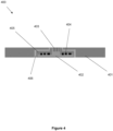
- FIG 4 shows another embodiment of a shielded apparatus 400 for obtaining ion energy distribution measurements in accordance with the present teachings.
- a conductive substrate 401 is provided in which a circuit board 402 having a sensor 403 and associated circuitry 404 is embedded.
- a conductive enclosure 405 surrounding the sensor 403 and associated circuitry 404 is also shown.
- an insulating layer 406 is provided between the conductive enclosure 405 and conductive substrate 401.
- the conductive enclosure 405 should be isolated from the conductive substrate 401. This is achieved by installing the insulating layer 406 between the conductive enclosure 405 and the conductive substrate 401 to break the continuity of the conductive enclosure 405 as shown in figure 4 .
- circuit board 402 having a sensor 403 and associated circuitry 404
- present embodiment is not limited to this and a plurality of circuit boards may be provided as described with respect to the embodiment of figure 3(a) .
- Figure 5 shows another embodiment of an apparatus 500 of the present teachings.
- a substrate 501 with circuit boards 502 in the substrate 501 are provided.
- Sensors 503 and electronic circuitry 504 are provided on the circuit boards 502.
- a conductive enclosure 505 surrounds each circuit board 502.
- the substrate 501 is formed from undoped silicon.
- the substrate 501 of the apparatus 500 in accordance with the present teachings can be manufactured from silicon.
- these can be formed from doped silicon.
- silicon based substrates it is advantageous from a manufacturing point of view to avoid the need to dope the silicon to make it conductive.
- Silicon is considered a semiconductor (neither conductor nor insulator). Germanium or another semiconductor material can also be used.
- a silicon cover 506 is also provided on the bottom side of the substrate 501. That, is the silicon cover 506 is provided on an opposite side of the substrate to which the plasma is detected by the sensors 503. This is useful when the silicon substrate based apparatus 500 is used in a semiconductor production process since the machine will be handling silicon wafers. Therefore, it is desirable to build an imitation wafer probe where all exposed surfaces are made from silicon. This minimises the risk of contamination of the machine by the wafer probe.
- a silicon cover or a cover formed from another material may also be used with the other embodiments described herein. That is, a cover may be provided on the underside of any of the apparatuses described herein.
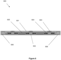
- FIG. 6 shows a further embodiment of an apparatus 600 for obtaining ion energy distribution measurements in a plasma processing system.
- the apparatus comprises a non-conducting substrate 601 and a plurality of circuit boards 602.
- each circuit board 602 includes a sensor 603 and associated control circuitry 604.
- a single conductive enclosure 605 surrounds the plurality of circuit boards 602 such that none of the substrate 601 is within the conductive enclosure 605.
- An RF (loop) antenna 606 is also provided in the non-conducting substrate 601.
- the antenna is connected back into the control circuitry 604 within the conductive enclosure 605.
- This antenna 606 is used for communicating data off the apparatus 600 in real-time while the plasma is running, where digitised sensor measurements can be encoded onto the antenna by switching it on and off to modulate the power flow into the chamber at a very low level. This modulation can be sensed on the power feed line.
- loop antenna 606 Although only one rectangular loop antenna 606 is shown in the cross-section view of figure 6 , a plurality of loop antennas 606 may be provided. 100's of connected loops right around the wafer edge can also be provided. In addition, the loop antennas may be broken into a few sections that can be switched in and out of the apparatus.
- circuit board 602 While the apparatus if figure 6 is shown with multiple circuit boards 602, only a single circuit board may be provided with one or more loop antennas.
- the conductive enclosure needs to surround the circuitry and all sensing elements in one continuous shield. This would have the configuration of a circular disk in the centre (housing the circuitry) and extending out on spokes to each sensor position. The antenna would circumnavigates the edge of the wafer.
- RF antennas for real time communication cannot be installed in conducting material (conducting substrate) as commonly used in known imitation wafer probes. RF current must be allowed to flow through the wafer cross-section (from bottom to top) to activate the antennas.
- the RF antenna may also be provided in a semi-conductive region of the substrate.
- this shows a perspective view of the previously described circuit board and associated sensor's conductive enclosure 700, which can be embedded in the substrate of any of the apparatuses described herein.
- a sensor located inside the raised section 701 with apertures 702 on the top surface thereof is shown.
- the apertures 702 form an array manufactured in the top surface of the conductive enclosure.
- the top surface of 702 may be exposed to the plasma and flush with the top surface of the substrate assembly. Alternatively, the top surface of 702 may sit just below a top layer of the substrate, where a matching array of apertures are formed therein, constituting the plasma facing surface of the wafer probe. Plasma species may enter the sensor through 702 for analysis.
- the sampling apertures 702 can be sub millimetre in diameter and must provide sufficient open area to deliver adequate charged particle flux for detection.
- the previously described control circuitry or any other components needed for the operation of the imitation wafer probe may be provided in a cavity within section 703 of the circuit board and sensor enclosure 700.
- the shape and scale of the conductive enclosure 700 depicted in figure 7 , wherein the sensor stack and circuit are disposed, is for illustrative purposes only.
- the conductive enclosure 700 may take any suitable form factor.
Landscapes
- Engineering & Computer Science (AREA)
- Chemical & Material Sciences (AREA)
- Analytical Chemistry (AREA)
- Physics & Mathematics (AREA)
- Plasma & Fusion (AREA)
- Power Engineering (AREA)
- Microelectronics & Electronic Packaging (AREA)
- General Physics & Mathematics (AREA)
- Drying Of Semiconductors (AREA)
- Plasma Technology (AREA)
- Electron Sources, Ion Sources (AREA)
Abstract
Description
- The present application relates to shielding the components of an imitation wafer probe used for measuring the incident charged particle current densities and energy distributions arriving at a surface of the probe during plasma processing.
- Plasma processing is used extensively in modern industry for a wide range of applications. A well-known example is the manufacture of integrated circuits in the semiconductor industry. Plasma processing is also used in the production of solar panels, flat panel displays, thin film coatings and medical devices, among many others.
- The ion current density (ion flux) and energy distribution (IED) of the ions arriving at a substrate surface strongly influence the performance of plasma based processes. In semiconductor manufacturing the substrate is typically a silicon wafer while in other industries the substrate may be glass panel or a variety of alternatives. Wafer and substrate may be used interchangeably through the document but understood to mean any type of substrate to be used in a plasma process. Throughout the process the substrate surface is bombarded by plasma species, including energetic ions, to remove (etch) and/or deposit layers of material to form structures or features on the workpiece surface. Ion impact may drive the etching and deposition directly, or may be used to activate the surface for more reactive plasma species to do the work. For example, in the plasma etching of features in the semiconductor industry the ion flux and associated IED determines important parameters such as etch rate, etch selectivity and etch anisotropy. The IED is therefore a critical plasma parameter to measure, understand and control to ensure optimum process performance.
- As the scale-down of transistor critical dimensions continues, tighter control of the IED at the wafer surface is required. Repeatability and uniformity of the IED is critical for optimal process yield. Wafer and substrate integrated IED probes are therefore essential to the advancement of nanotechnology manufactured using plasma processing.
- A variety of probes have been developed over many decades to measure the IED in plasma processes. The planar, retarding field analyser (RFA) design is well known. In many RFA embodiments, a stack of conductive grids, individually separated by insulators, is used to separate ions based on their energy and hence determine the IED. An aperture facing the plasma allows a sample of ions into the probe for analysis. A succession of grids are used to a) prevent plasma penetration inside the device, b) repel plasma electrons, c) discriminate ions based on their energies and d) prevent secondary electron emission from the collector electrode. The collector electrode terminates the stack and is used to detect the ion current signal for measurement. The ion current is recorded for each retarding voltage applied to the ion energy discrimination grid to give an integral form of the energy distribution. The tabulated ion current versus discriminator grid voltage data is numerically differentiated to determine the IED.
- Imitation substrates with embedded sensors have been the subject of numerous inventions. Some of these inventions focus on sensor designs and their construction, while others focus on the electronic control platform for processing, storing and transmitting the sensor data. The electronic platform is either fully integrated into the imitation substrate with its own power supply or is decoupled from the imitation substrate using interconnecting wires which pass through the chamber wall, using vacuum feedthroughs, to the electronic control platform located on the air side.
- It is known that the electronics within such sensors and associated circuitry in the substrate must be protected from electromagnetic radiation generated by the plasma process. In prior art designs where the electronic control system and power supply is fully integrated into an imitation wafer probe, undesirable electric field formation can also occur and distort the IED measurements. A Faraday shield is usually provided in such prior art sensors to address these issues.
-
EP 3968353 discloses an apparatus for obtaining ion energy distribution measurements in a plasma processing system comprising, a substrate for placement in the plasma processing system for exposure to the plasma, an ion energy analyser disposed in the substrate for measuring the ion energy distribution at the substrate surface during plasma processing, the analyser comprising a plurality of grids a rechargeable battery power supply including control circuitry, integrated in the substrate, for supplying voltage to each of the grids and the collector of the ion energy analyser. A Faraday shield is provided encasing the ion energy analyser, the power supply and the control circuitry. -
US 2011 0174777 teaches embedding sensors and their corresponding power supplying and controlling electronics directly in a diagnostic wafer in order to facilitate the in-situ measurements of plasma properties during plasma operation. This prior art document also teaches protecting said electronics by means of a Faraday shield. -
US 8,104,342 provides an instrument for measuring a parameter comprising a substrate, a plurality of sensors carried by and distributed across a surface of the substrate that individually measure the parameter at different positions, an electronic processing component carried by the substrate surface, electrical conductors extending across the surface connected to the sensors and the electronic processing component, and a cover disposed over the sensors, electronic processing component and conductors. -
WO 2007/130790 describes a process condition measuring device for measuring a process condition in a processing system that processes workpieces of standard dimensions, comprising a first conductive substrate portion, a second conductive substrate portion, an electrical circuit interposed between the first conductive substrate portion and the second conductive substrate portion, and the first and second conductive substrate portions electrically connected together to form an electrically continuous body that has at least one dimension that is equal to a dimension of a workpiece processed by the processing system. - Some real production wafers are known to develop non-uniform charge build up across the surface. The DC bias potential induced by RF power delivery to the wafer can also be non-uniform across the wafer surface, resulting in non-uniform IED's at different points on the wafer. The formation of an electrically continuous body (to provide a shield) in an imitation wafer probe forces a uniform charge distribution across the surface and forces the DC bias potential to be the same at every point, where the shield becomes an equipotential surface. Therefore, the locally measured IED in the presence of such a shield can be a distorted version of the true IED at that location on a real production wafer.
- With such known configurations, RF current is forced to flow around the outside of the continuous shield and not through the wafer. This can also be a problem for some applications.
- There are a number of shortcomings with the shielding provided by the prior art imitation substrate probes. There is a need to address these shortcomings.
- The present teachings describe an apparatus or imitation wafer probe for obtaining ion energy distribution measurements in a plasma processing system comprising a substrate, an ion energy sensor and associated control circuitry disposed in the substrate, and a conductive enclosure disposed in the substrate and surrounding the ion energy sensor and control circuitry such that the substrate at least partially surrounds the conductive enclosure.
- The substrate may be conductive or non-conductive.
- The apparatus may further comprise an insulating layer between the substrate and the conductive enclosure.
- The substrate may be semi-conducting. Optionally, the substrate is silicon.
- The apparatus may further comprise a semi-conducting cover on a surface of the substrate. The semi-conducting cover may be made from silicon.
- Optionally, the ion energy sensor measures energy distribution at a first surface of the substrate and the cover is provided at a second surface of the substrate opposite to the first surface.
- The apparatus may further comprise an RF antenna disposed in the substrate outside of the conductive enclosure.
- The apparatus may further comprise a plurality of sensors, each sensor having control circuitry, wherein the conductive enclosure surrounds the plurality of sensors and control circuitry.
- The control circuitry may be confined to a central area of the substrate and the sensors are spatially dispersed across the substrate.
- Optionally, the RF antenna is connected to the control circuitry.
- The RF antenna may be provided at the periphery of the substrate in a non-conductive or semi-conductive region.
- Each ion energy sensor and control circuitry may be provided on a circuit board.
- The present application will now be described with reference to the accompanying drawings in which:
-
Fig. 1 shows an overview of a system for use with an imitation wafer probe in accordance with the present teachings; -
Fig. 2 shows an array of sensors for measuring IED distributed across the surface of an imitation wafer probe; -
Fig. 3(a) shows a first embodiment of a shielded apparatus (imitation wafer probe) in accordance with the present teachings; -
Fig. 3(b) shows another embodiment of the shielded apparatus; -
Fig. 4 shows a further embodiment of a shielded apparatus in accordance with the present teachings; -
Fig. 5 shows another embodiment of a shielded apparatus; -
Fig. 6 shows a further embodiment of a shielded apparatus in accordance with the present teachings; and -
Fig. 7 shows a perspective view of a circuit board for use in a shielded apparatus of the present teachings. -
Figure 1 illustrates an overview of asystem 100 that is capable of measuring the ion energy distribution arriving at the surface of animitation wafer probe 101 surface during plasma processing. In this particular illustration, thediagnostic system 100 includes animitation wafer probe 101 with integrated ion energy sensors and control electronic circuitry including battery power supply and wireless communication etc. The diagnostic system further comprises adocking station 102 withintegrated wireless transponder 103 to enableimitation wafer probe 101 charging, configuration and data retrieval. Thedocking station 102 is equipped with Ethernet connectivity to communicate with ahost PC 104. Application software is provided to display and analyse retrieved data. The application software provides a control panel for scheduling the experimental assignments. An advanced programming interface (API) is also provided to allow direct interaction between the docking station and factory control software. - A four chamber
plasma processing system 105 is also shown infigure 1 . This is one of many different types of plasma processing system and is merely used to illustrate the functionality of theimitation wafer probe 101 in accordance with the present teachings. Theplasma processing system 105 may have one or moreinterconnected processing chambers 106. Eachprocessing chamber 106 is equipped with vacuum pumps to evacuate the chamber, gas flow controls to set the process recipe, vacuum gauges and transducers to regulate process operating pressure, power delivery mechanism to excite the chemical recipe to the plasma state and a pedestal to hold the substrate during processing. Aload lock chamber 108 withrobotic transfer mechanism 107 is used to transport substrates to and from the processing chambers. Substrate batches are delivered to theload lock chamber 108 through a cassette or FOUP. - The
imitation probe 101 is placed in thedocking station 102 and communication is established through the application software on thehost PC 104. The battery power supply on thewafer probe 101 is charged, stored data retrieved and the next experimental assignment scheduled to prime thewafer probe 101. Theimitation wafer probe 101 is then placed in an available slot in a Front Opening Universal Pod (FOUP) which is subsequently delivered to theload lock chamber 108. Therobotic arm 107 transports theimitation wafer probe 101 to theprocessing chamber 106 and positions it on a processing pedestal in preparation for plasma exposure. With thechamber 106 already under vacuum, the process recipe is configured and plasma ignited. When plasma is formed, plasma species begin to bombard thewafer probe 101, a sample of which enters the sensors of theprobe 101 for analysis. Analysis proceeds at the times configured in the scheduler if the on-board pressure sensor reports that the threshold for high voltage application has been met. This safety mechanism prevents the accidental application of high voltage at atmospheric pressure, which could destroy the sensor due to electrical arcing. If the pressure threshold has been met, thewafer probe 101 is activated at the scheduled time. The appropriate voltages are applied to all the grids and collector, the collector current is recorded as a function of ion discrimination potential by a microcontroller (MCU), not shown, and the resultant data is stored in memory. Thewafer probe 101 returns to sleep mode until the next scheduled measurement, at which point the process is repeated. When the assignment is completed, the plasma process may be terminated to allow retrieval of thewafer probe 101 from the processing pedestal using the robotic arm which transports the wafer probe back through theload lock chamber 108 to the FOUP. The user extracts thewafer probe 101 from the FOUP and places it back in thedocking station 102 for data retrieval, recharging and scheduling of the next experimental assignment. Alternatively, it is possible for the wafer probe to transmit the sensor data in real-time to the docking station, from its location inside the processing chamber, using known wireless communication apparatus and methodology. - It should be appreciated that the
wafer probe 101 in accordance with the present teachings is not limited for use in the system as shown infigure 1 and any suitable system may be chosen. - The configuration of the
wafer probe 101 will now be described in more detail. In the preferred embodiment thewafer probe 101 is fabricated on a substrate to mimic the standard semiconductor work piece. It may be manufactured using silicon, ceramic, metal, glass or any other material to mimic the types of substrates used in plasma processing, and may have the same geometry as a standard substrate with substantively the same dimensions and weight. The general configuration of theimitation wafer probe 101 is shown infigure 2 which depicts an array ofsensors 201 distributed across the surface of asemiconductor wafer probe 101. In particular,figure 2 shows a plan view of awafer probe 101 with ninesensors 201, thesesensors 201 are used for measurement of ion energy distribution at the substrate surface of thewafer probe 101. Theimitation wafer probe 101 may comprise a single sensor 202 (at any location) or comprise a plurality of spatially distributedsensors 201. - The
sensors 201 may comprise alternating layers of planar, parallel, conductive metal grids and insulators, the grids being electrically polarised in a systematic way to filter out plasma electrons, separate positive ions based on their energy, suppress secondary electron emission and collect ion current for measurement. The sensors are embedded in the substrate of the imitation afterprobe 101. The sensor configuration shown inEP 3968353 . However, it should be appreciated that the specific configuration of thesensors 201 used with theimitation wafer probe 101 is not the focus of the present application and any suitable sensor configuration may be used. Rather, the present teachings provide improved techniques for shielding the sensor and associated electronics within the substrate of theimitation probe 101. - Turning to
figure 3(a) , a first embodiment of a shielded apparatus (imitation wafer probe) for obtaining ion energy distribution measurements in a plasma processing system is provided. Theapparatus 300 includes anon-conducting substrate 301. A plurality ofcircuit boards 302 are provided within theapparatus 300 i.e., within thesubstrate 301. Eachcircuit board 302 includes a sensor 303 (such as a known grid stack) and associatedcontrol circuitry 304. As in known to the person skilled in the art, apertures are manufactured in the plasma facing surface of thesubstrate 301 and constitute the top surface of the apparatus. In one embodiment the substrate is a 100mm, 150mm, 200mm, 300mm or 450mm diameter silicon wafer, but any other material, geometry or dimensions can be used in the manufacture of the wafer probe as required by the application. The control circuitry includes an on board power supply, such as a rechargeable battery, and any other circuitry necessary for operation of theapparatus 300. An antenna may also be provided for charging the battery and communicating with the docking station. - To protect the sensors and associated circuitry, a
conductive enclosure 305 is provided surrounding eachcircuit board 302. It can be seen that thesubstrate 301 at least partially surrounds eachconductive enclosure 305. - In order to measure ion energy and ion flux uniformity, it is important to ensure the distributed
sensors 303 are electrically isolated from each other. Therefore, it is advantageous for thesensors 303 to be independently shielded using a conductive enclosure for eachsensor 303. This ensures the sensors and associated circuitry are electrically isolated from each other. This in turn allows eachsensor 303 to detect exactly what is happening at its respective location without being influenced by an artificially created continuous shield surrounding the device, which may not be representative of the real situation. That is, the absence of an artificially created continuous shield surrounding the device results in more accurate sensor measurements. - In the embodiment of
figure 3(a) the electrically shielded sensors 303 (and associated circuitry) are provided in a non-conducting substrate. This replicates the conditions "seen" by a non-conducting substrate during processing. - Turning to
figure 3(b) , this shows the embodiment offigure 3(a) wherein only asingle circuit board 302 with asingle sensor 303 is provided in thesubstrate 301 of theapparatus 306. This variation on the embodiment offigure 3(a) also ensures thesensor 303 can detect exactly what is happening at its location. Since an artificially created continuous shield surrounding the entire device/apparatus is not provided then this cannot interfere with sensor measurements. - Turning to
figure 4 , this shows another embodiment of a shieldedapparatus 400 for obtaining ion energy distribution measurements in accordance with the present teachings. Aconductive substrate 401 is provided in which acircuit board 402 having asensor 403 and associatedcircuitry 404 is embedded. Aconductive enclosure 405 surrounding thesensor 403 and associatedcircuitry 404 is also shown. In addition, an insulatinglayer 406 is provided between theconductive enclosure 405 andconductive substrate 401. - In this embodiment, when a
conductive substrate 401 is used, it is important to break the naturally formed continuous electrical shield, which could form around theconductive substrate 401. In particular, in the case of a conducting substrate, the rf potential across the surface of the substrate can be non-uniform. To ensure that a true measurement of the plasma conditions at the sensor location is achieved, the conductive enclosure 405 (sensor shield) should be isolated from theconductive substrate 401. This is achieved by installing the insulatinglayer 406 between theconductive enclosure 405 and theconductive substrate 401 to break the continuity of theconductive enclosure 405 as shown infigure 4 . - While the embodiment of
figure 4 is shown with only onecircuit board 402 having asensor 403 and associatedcircuitry 404 the present embodiment is not limited to this and a plurality of circuit boards may be provided as described with respect to the embodiment offigure 3(a) . -
Figure 5 shows another embodiment of anapparatus 500 of the present teachings. As previously described, asubstrate 501 withcircuit boards 502 in thesubstrate 501 are provided.Sensors 503 andelectronic circuitry 504 are provided on thecircuit boards 502. Aconductive enclosure 505 surrounds eachcircuit board 502. - The
substrate 501 is formed from undoped silicon. As previously mentioned, thesubstrate 501 of theapparatus 500 in accordance with the present teachings can be manufactured from silicon. For the previously described conductive substrates, these can be formed from doped silicon. However, for silicon based substrates, it is advantageous from a manufacturing point of view to avoid the need to dope the silicon to make it conductive. Silicon is considered a semiconductor (neither conductor nor insulator). Germanium or another semiconductor material can also be used. - In the undoped silicon substrate embodiment of
figure 5 , asilicon cover 506 is also provided on the bottom side of thesubstrate 501. That, is thesilicon cover 506 is provided on an opposite side of the substrate to which the plasma is detected by thesensors 503. This is useful when the silicon substrate basedapparatus 500 is used in a semiconductor production process since the machine will be handling silicon wafers. Therefore, it is desirable to build an imitation wafer probe where all exposed surfaces are made from silicon. This minimises the risk of contamination of the machine by the wafer probe. - A silicon cover or a cover formed from another material may also be used with the other embodiments described herein. That is, a cover may be provided on the underside of any of the apparatuses described herein.
-
Figure 6 shows a further embodiment of anapparatus 600 for obtaining ion energy distribution measurements in a plasma processing system. The apparatus comprises anon-conducting substrate 601 and a plurality ofcircuit boards 602. As previously described, eachcircuit board 602 includes asensor 603 and associatedcontrol circuitry 604. A singleconductive enclosure 605 surrounds the plurality ofcircuit boards 602 such that none of thesubstrate 601 is within theconductive enclosure 605. - An RF (loop)
antenna 606 is also provided in thenon-conducting substrate 601. The antenna is connected back into thecontrol circuitry 604 within theconductive enclosure 605. Thisantenna 606 is used for communicating data off theapparatus 600 in real-time while the plasma is running, where digitised sensor measurements can be encoded onto the antenna by switching it on and off to modulate the power flow into the chamber at a very low level. This modulation can be sensed on the power feed line. - Although only one
rectangular loop antenna 606 is shown in the cross-section view offigure 6 , a plurality ofloop antennas 606 may be provided. 100's of connected loops right around the wafer edge can also be provided. In addition, the loop antennas may be broken into a few sections that can be switched in and out of the apparatus. - While the apparatus if
figure 6 is shown withmultiple circuit boards 602, only a single circuit board may be provided with one or more loop antennas. - For certain applications, it is desirable to centralise all circuitry (and power supplies), while the sensors are distributed at various locations around the wafer. For this embodiment, the conductive enclosure needs to surround the circuitry and all sensing elements in one continuous shield. This would have the configuration of a circular disk in the centre (housing the circuitry) and extending out on spokes to each sensor position. The antenna would circumnavigates the edge of the wafer.
- RF antennas (loops) for real time communication cannot be installed in conducting material (conducting substrate) as commonly used in known imitation wafer probes. RF current must be allowed to flow through the wafer cross-section (from bottom to top) to activate the antennas. The RF antenna may also be provided in a semi-conductive region of the substrate.
- With reference to
figure 7 , this shows a perspective view of the previously described circuit board and associated sensor'sconductive enclosure 700, which can be embedded in the substrate of any of the apparatuses described herein. A sensor located inside the raisedsection 701 withapertures 702 on the top surface thereof is shown. Theapertures 702 form an array manufactured in the top surface of the conductive enclosure. The top surface of 702 may be exposed to the plasma and flush with the top surface of the substrate assembly. Alternatively, the top surface of 702 may sit just below a top layer of the substrate, where a matching array of apertures are formed therein, constituting the plasma facing surface of the wafer probe. Plasma species may enter the sensor through 702 for analysis. Thesampling apertures 702 can be sub millimetre in diameter and must provide sufficient open area to deliver adequate charged particle flux for detection. The previously described control circuitry or any other components needed for the operation of the imitation wafer probe may be provided in a cavity withinsection 703 of the circuit board andsensor enclosure 700. The shape and scale of theconductive enclosure 700 depicted infigure 7 , wherein the sensor stack and circuit are disposed, is for illustrative purposes only. Theconductive enclosure 700 may take any suitable form factor. - The invention is not limited to the embodiment(s) described herein but can be amended or modified without departing from the scope of the present invention.
Claims (15)
- An apparatus for obtaining ion energy distribution measurements in a plasma processing system comprising:a substrate;an ion energy sensor and associated control circuitry disposed in the substrate; anda conductive enclosure disposed in the substrate and surrounding the ion energy sensor and control circuitry such that the substrate at least partially surrounds the conductive enclosure.
- The apparatus of claim 1, wherein the substrate is non-conductive.
- The apparatus of claim 1, wherein the substrate is conductive.
- The apparatus of claim 3, further comprising an insulating layer between the substrate and the conductive enclosure.
- The apparatus of claim 1, wherein the substrate is semi-conducting.
- The apparatus of claim 5, wherein the substrate is silicon.
- The apparatus of claim 5 or 6, further comprising a semi-conducting cover on a surface of the substrate.
- The apparatus of claim 7, wherein the semi-conducting cover is silicon or Germanium.
- The apparatus of claim 7 or 8, wherein the ion energy sensor measures energy distribution at a first surface of the substrate and a cover is provided at a second surface of the substrate opposite to the first surface.
- The apparatus of claim 2, further comprising an RF antenna disposed in the substrate outside of the conductive enclosure.
- The apparatus of claim 10, comprising a plurality of sensors, each sensor having control circuitry, wherein the conductive enclosure surrounds the plurality of sensors and control circuitry.
- The apparatus of claim 11, wherein the control circuitry is confined to a central area of the substrate and the sensors are spatially dispersed across the substrate.
- The apparatus of any one of claims 10 to 12, wherein the RF antenna is connected to the control circuitry.
- The apparatus of any one of claims 10 to 13, wherein the RF antenna is disposed in the non-conductive substrate
- The apparatus of any one of claims 1 to 14, wherein each ion energy sensor and control circuitry are provided on a circuit board.
Priority Applications (7)
| Application Number | Priority Date | Filing Date | Title |
|---|---|---|---|
| EP25190842.2A EP4625471A3 (en) | 2022-11-25 | 2022-11-25 | Shielded device for ion energy analysis of plasma processes |
| EP22209525.9A EP4376050B1 (en) | 2022-11-25 | 2022-11-25 | Shielded apparatus for ion energy analysis of plasma processes |
| TW112144339A TW202437307A (en) | 2022-11-25 | 2023-11-16 | Shielded apparatus for ion energy analysis of plasma processes |
| JP2023196354A JP2024076991A (en) | 2022-11-25 | 2023-11-20 | Shielded apparatus for ion energy analysis of plasma processing. |
| US18/515,593 US20240177965A1 (en) | 2022-11-25 | 2023-11-21 | Shielded apparatus for ion energy analysis of plasma processes |
| CN202311570603.0A CN118098918A (en) | 2022-11-25 | 2023-11-23 | Shielding for ion energy analysis in plasma processing |
| KR1020230165893A KR20240078388A (en) | 2022-11-25 | 2023-11-24 | Shielded Apparatus for Ion Energy Analysis of Plasma Processes |
Applications Claiming Priority (1)
| Application Number | Priority Date | Filing Date | Title |
|---|---|---|---|
| EP22209525.9A EP4376050B1 (en) | 2022-11-25 | 2022-11-25 | Shielded apparatus for ion energy analysis of plasma processes |
Related Child Applications (1)
| Application Number | Title | Priority Date | Filing Date |
|---|---|---|---|
| EP25190842.2A Division EP4625471A3 (en) | 2022-11-25 | 2022-11-25 | Shielded device for ion energy analysis of plasma processes |
Publications (2)
| Publication Number | Publication Date |
|---|---|
| EP4376050A1 true EP4376050A1 (en) | 2024-05-29 |
| EP4376050B1 EP4376050B1 (en) | 2025-07-23 |
Family
ID=84363098
Family Applications (2)
| Application Number | Title | Priority Date | Filing Date |
|---|---|---|---|
| EP25190842.2A Pending EP4625471A3 (en) | 2022-11-25 | 2022-11-25 | Shielded device for ion energy analysis of plasma processes |
| EP22209525.9A Active EP4376050B1 (en) | 2022-11-25 | 2022-11-25 | Shielded apparatus for ion energy analysis of plasma processes |
Family Applications Before (1)
| Application Number | Title | Priority Date | Filing Date |
|---|---|---|---|
| EP25190842.2A Pending EP4625471A3 (en) | 2022-11-25 | 2022-11-25 | Shielded device for ion energy analysis of plasma processes |
Country Status (6)
| Country | Link |
|---|---|
| US (1) | US20240177965A1 (en) |
| EP (2) | EP4625471A3 (en) |
| JP (1) | JP2024076991A (en) |
| KR (1) | KR20240078388A (en) |
| CN (1) | CN118098918A (en) |
| TW (1) | TW202437307A (en) |
Families Citing this family (2)
| Publication number | Priority date | Publication date | Assignee | Title |
|---|---|---|---|---|
| KR20240115067A (en) * | 2023-01-18 | 2024-07-25 | 삼성전자주식회사 | Plasma diagnostic apparatus and operating method thereof |
| CN118919387B (en) * | 2024-10-10 | 2025-01-24 | 上海邦芯半导体科技有限公司 | Ion density detection device and ion density measurement method thereof |
Citations (7)
| Publication number | Priority date | Publication date | Assignee | Title |
|---|---|---|---|---|
| US5451784A (en) * | 1994-10-31 | 1995-09-19 | Applied Materials, Inc. | Composite diagnostic wafer for semiconductor wafer processing systems |
| WO2007130790A2 (en) | 2006-05-01 | 2007-11-15 | Sensarray Corporation | Process condition measuring device with shielding |
| US20090242790A1 (en) * | 2008-03-31 | 2009-10-01 | Tokyo Electron Limited | Ion energy analyzer and methods of manufacturing and operating |
| US20110174777A1 (en) | 2010-01-21 | 2011-07-21 | Kla-Tencor Corporation | Process condition sensing device and method for plasma chamber |
| US8104342B2 (en) | 2007-02-23 | 2012-01-31 | Kla-Tencor Corporation | Process condition measuring device |
| GB2547729A (en) * | 2016-02-29 | 2017-08-30 | Cirrus Logic Int Semiconductor Ltd | Integrated MEMS transducer and circuitry |
| EP3968353A1 (en) | 2020-09-10 | 2022-03-16 | Impedans Ltd | Apparatus for ion energy analysis of plasma processes |
Family Cites Families (5)
| Publication number | Priority date | Publication date | Assignee | Title |
|---|---|---|---|---|
| US20060171848A1 (en) * | 2005-01-31 | 2006-08-03 | Advanced Energy Industries, Inc. | Diagnostic plasma sensors for endpoint and end-of-life detection |
| KR100782370B1 (en) * | 2006-08-04 | 2007-12-07 | 삼성전자주식회사 | Ion Analysis System Based on Ion Energy Distribution Analyzer Using Delayed Electric Field |
| US7777179B2 (en) * | 2008-03-31 | 2010-08-17 | Tokyo Electron Limited | Two-grid ion energy analyzer and methods of manufacturing and operating |
| US9087677B2 (en) * | 2011-03-28 | 2015-07-21 | Tokyo Electron Limited | Methods of electrical signaling in an ion energy analyzer |
| US10083883B2 (en) * | 2016-06-20 | 2018-09-25 | Applied Materials, Inc. | Wafer processing equipment having capacitive micro sensors |
-
2022
- 2022-11-25 EP EP25190842.2A patent/EP4625471A3/en active Pending
- 2022-11-25 EP EP22209525.9A patent/EP4376050B1/en active Active
-
2023
- 2023-11-16 TW TW112144339A patent/TW202437307A/en unknown
- 2023-11-20 JP JP2023196354A patent/JP2024076991A/en active Pending
- 2023-11-21 US US18/515,593 patent/US20240177965A1/en active Pending
- 2023-11-23 CN CN202311570603.0A patent/CN118098918A/en active Pending
- 2023-11-24 KR KR1020230165893A patent/KR20240078388A/en active Pending
Patent Citations (7)
| Publication number | Priority date | Publication date | Assignee | Title |
|---|---|---|---|---|
| US5451784A (en) * | 1994-10-31 | 1995-09-19 | Applied Materials, Inc. | Composite diagnostic wafer for semiconductor wafer processing systems |
| WO2007130790A2 (en) | 2006-05-01 | 2007-11-15 | Sensarray Corporation | Process condition measuring device with shielding |
| US8104342B2 (en) | 2007-02-23 | 2012-01-31 | Kla-Tencor Corporation | Process condition measuring device |
| US20090242790A1 (en) * | 2008-03-31 | 2009-10-01 | Tokyo Electron Limited | Ion energy analyzer and methods of manufacturing and operating |
| US20110174777A1 (en) | 2010-01-21 | 2011-07-21 | Kla-Tencor Corporation | Process condition sensing device and method for plasma chamber |
| GB2547729A (en) * | 2016-02-29 | 2017-08-30 | Cirrus Logic Int Semiconductor Ltd | Integrated MEMS transducer and circuitry |
| EP3968353A1 (en) | 2020-09-10 | 2022-03-16 | Impedans Ltd | Apparatus for ion energy analysis of plasma processes |
Also Published As
| Publication number | Publication date |
|---|---|
| KR20240078388A (en) | 2024-06-03 |
| CN118098918A (en) | 2024-05-28 |
| TW202437307A (en) | 2024-09-16 |
| EP4625471A3 (en) | 2025-12-31 |
| EP4625471A2 (en) | 2025-10-01 |
| US20240177965A1 (en) | 2024-05-30 |
| EP4376050B1 (en) | 2025-07-23 |
| JP2024076991A (en) | 2024-06-06 |
Similar Documents
| Publication | Publication Date | Title |
|---|---|---|
| EP3968354B1 (en) | Apparatus for ion energy analysis of plasma processes | |
| US10431434B2 (en) | Powered grid for plasma chamber | |
| US20240177965A1 (en) | Shielded apparatus for ion energy analysis of plasma processes | |
| EP1884984B1 (en) | Ion analysis system based on analyzer of ion energy distribution using retarded electric field | |
| US20250118541A1 (en) | Plasma processing apparatus | |
| US20090242790A1 (en) | Ion energy analyzer and methods of manufacturing and operating | |
| WO2002023583A9 (en) | Monitor system and method for semiconductor processes | |
| TW202601131A (en) | Wireless measurement characterization | |
| EP1269513B1 (en) | Inductively coupled plasma etching apparatus |
Legal Events
| Date | Code | Title | Description |
|---|---|---|---|
| PUAI | Public reference made under article 153(3) epc to a published international application that has entered the european phase |
Free format text: ORIGINAL CODE: 0009012 |
|
| STAA | Information on the status of an ep patent application or granted ep patent |
Free format text: STATUS: THE APPLICATION HAS BEEN PUBLISHED |
|
| AK | Designated contracting states |
Kind code of ref document: A1 Designated state(s): AL AT BE BG CH CY CZ DE DK EE ES FI FR GB GR HR HU IE IS IT LI LT LU LV MC ME MK MT NL NO PL PT RO RS SE SI SK SM TR |
|
| STAA | Information on the status of an ep patent application or granted ep patent |
Free format text: STATUS: REQUEST FOR EXAMINATION WAS MADE |
|
| 17P | Request for examination filed |
Effective date: 20241021 |
|
| RBV | Designated contracting states (corrected) |
Designated state(s): AL AT BE BG CH CY CZ DE DK EE ES FI FR GB GR HR HU IE IS IT LI LT LU LV MC ME MK MT NL NO PL PT RO RS SE SI SK SM TR |
|
| GRAP | Despatch of communication of intention to grant a patent |
Free format text: ORIGINAL CODE: EPIDOSNIGR1 |
|
| STAA | Information on the status of an ep patent application or granted ep patent |
Free format text: STATUS: GRANT OF PATENT IS INTENDED |
|
| RIC1 | Information provided on ipc code assigned before grant |
Ipc: H01J 49/48 20060101ALI20250210BHEP Ipc: H01J 37/32 20060101AFI20250210BHEP |
|
| INTG | Intention to grant announced |
Effective date: 20250311 |
|
| GRAS | Grant fee paid |
Free format text: ORIGINAL CODE: EPIDOSNIGR3 |
|
| GRAA | (expected) grant |
Free format text: ORIGINAL CODE: 0009210 |
|
| STAA | Information on the status of an ep patent application or granted ep patent |
Free format text: STATUS: THE PATENT HAS BEEN GRANTED |
|
| AK | Designated contracting states |
Kind code of ref document: B1 Designated state(s): AL AT BE BG CH CY CZ DE DK EE ES FI FR GB GR HR HU IE IS IT LI LT LU LV MC ME MK MT NL NO PL PT RO RS SE SI SK SM TR |
|
| REG | Reference to a national code |
Ref country code: GB Ref legal event code: FG4D |
|
| REG | Reference to a national code |
Ref country code: CH Ref legal event code: EP |
|
| REG | Reference to a national code |
Ref country code: IE Ref legal event code: FG4D |
|
| REG | Reference to a national code |
Ref country code: DE Ref legal event code: R096 Ref document number: 602022017992 Country of ref document: DE |
|
| REG | Reference to a national code |
Ref country code: CH Ref legal event code: W10 Free format text: ST27 STATUS EVENT CODE: U-0-0-W10-W00 (AS PROVIDED BY THE NATIONAL OFFICE) Effective date: 20251008 |
|
| REG | Reference to a national code |
Ref country code: DE Ref legal event code: R081 Ref document number: 602022017992 Country of ref document: DE Owner name: APPLIED MATERIALS, INC., SANTA CLARA, US Free format text: FORMER OWNER: IMPEDANS LTD, DUBLIN, IE Ref country code: DE Ref legal event code: R082 Ref document number: 602022017992 Country of ref document: DE Representative=s name: ZIMMERMANN & PARTNER PATENTANWAELTE MBB, DE |
|
| RAP2 | Party data changed (patent owner data changed or rights of a patent transferred) |
Owner name: APPLIED MATERIALS, INC. |
|
| REG | Reference to a national code |
Ref country code: GB Ref legal event code: 732E Free format text: REGISTERED BETWEEN 20251023 AND 20251029 |
|
| REG | Reference to a national code |
Ref country code: NL Ref legal event code: MP Effective date: 20250723 |
|
| PG25 | Lapsed in a contracting state [announced via postgrant information from national office to epo] |
Ref country code: PT Free format text: LAPSE BECAUSE OF FAILURE TO SUBMIT A TRANSLATION OF THE DESCRIPTION OR TO PAY THE FEE WITHIN THE PRESCRIBED TIME-LIMIT Effective date: 20251124 |
|
| PG25 | Lapsed in a contracting state [announced via postgrant information from national office to epo] |
Ref country code: NL Free format text: LAPSE BECAUSE OF FAILURE TO SUBMIT A TRANSLATION OF THE DESCRIPTION OR TO PAY THE FEE WITHIN THE PRESCRIBED TIME-LIMIT Effective date: 20250723 |
|
| REG | Reference to a national code |
Ref country code: AT Ref legal event code: MK05 Ref document number: 1817360 Country of ref document: AT Kind code of ref document: T Effective date: 20250723 |
|
| PG25 | Lapsed in a contracting state [announced via postgrant information from national office to epo] |
Ref country code: IS Free format text: LAPSE BECAUSE OF FAILURE TO SUBMIT A TRANSLATION OF THE DESCRIPTION OR TO PAY THE FEE WITHIN THE PRESCRIBED TIME-LIMIT Effective date: 20251123 |
|
| PGFP | Annual fee paid to national office [announced via postgrant information from national office to epo] |
Ref country code: DE Payment date: 20251022 Year of fee payment: 4 |
|
| PG25 | Lapsed in a contracting state [announced via postgrant information from national office to epo] |
Ref country code: NO Free format text: LAPSE BECAUSE OF FAILURE TO SUBMIT A TRANSLATION OF THE DESCRIPTION OR TO PAY THE FEE WITHIN THE PRESCRIBED TIME-LIMIT Effective date: 20251023 |
|
| REG | Reference to a national code |
Ref country code: LT Ref legal event code: MG9D |
|
| PG25 | Lapsed in a contracting state [announced via postgrant information from national office to epo] |
Ref country code: AT Free format text: LAPSE BECAUSE OF FAILURE TO SUBMIT A TRANSLATION OF THE DESCRIPTION OR TO PAY THE FEE WITHIN THE PRESCRIBED TIME-LIMIT Effective date: 20250723 |
|
| PG25 | Lapsed in a contracting state [announced via postgrant information from national office to epo] |
Ref country code: FI Free format text: LAPSE BECAUSE OF FAILURE TO SUBMIT A TRANSLATION OF THE DESCRIPTION OR TO PAY THE FEE WITHIN THE PRESCRIBED TIME-LIMIT Effective date: 20250723 |
|
| PG25 | Lapsed in a contracting state [announced via postgrant information from national office to epo] |
Ref country code: HR Free format text: LAPSE BECAUSE OF FAILURE TO SUBMIT A TRANSLATION OF THE DESCRIPTION OR TO PAY THE FEE WITHIN THE PRESCRIBED TIME-LIMIT Effective date: 20250723 |
|
| PGFP | Annual fee paid to national office [announced via postgrant information from national office to epo] |
Ref country code: FR Payment date: 20251023 Year of fee payment: 4 |
|
| PG25 | Lapsed in a contracting state [announced via postgrant information from national office to epo] |
Ref country code: GR Free format text: LAPSE BECAUSE OF FAILURE TO SUBMIT A TRANSLATION OF THE DESCRIPTION OR TO PAY THE FEE WITHIN THE PRESCRIBED TIME-LIMIT Effective date: 20251024 |
|
| PG25 | Lapsed in a contracting state [announced via postgrant information from national office to epo] |
Ref country code: SE Free format text: LAPSE BECAUSE OF FAILURE TO SUBMIT A TRANSLATION OF THE DESCRIPTION OR TO PAY THE FEE WITHIN THE PRESCRIBED TIME-LIMIT Effective date: 20250723 |
|
| PG25 | Lapsed in a contracting state [announced via postgrant information from national office to epo] |
Ref country code: LV Free format text: LAPSE BECAUSE OF FAILURE TO SUBMIT A TRANSLATION OF THE DESCRIPTION OR TO PAY THE FEE WITHIN THE PRESCRIBED TIME-LIMIT Effective date: 20250723 |
|
| PG25 | Lapsed in a contracting state [announced via postgrant information from national office to epo] |
Ref country code: PL Free format text: LAPSE BECAUSE OF FAILURE TO SUBMIT A TRANSLATION OF THE DESCRIPTION OR TO PAY THE FEE WITHIN THE PRESCRIBED TIME-LIMIT Effective date: 20250723 Ref country code: BG Free format text: LAPSE BECAUSE OF FAILURE TO SUBMIT A TRANSLATION OF THE DESCRIPTION OR TO PAY THE FEE WITHIN THE PRESCRIBED TIME-LIMIT Effective date: 20250723 |
|
| PG25 | Lapsed in a contracting state [announced via postgrant information from national office to epo] |
Ref country code: RS Free format text: LAPSE BECAUSE OF FAILURE TO SUBMIT A TRANSLATION OF THE DESCRIPTION OR TO PAY THE FEE WITHIN THE PRESCRIBED TIME-LIMIT Effective date: 20251023 |
|
| PG25 | Lapsed in a contracting state [announced via postgrant information from national office to epo] |
Ref country code: ES Free format text: LAPSE BECAUSE OF FAILURE TO SUBMIT A TRANSLATION OF THE DESCRIPTION OR TO PAY THE FEE WITHIN THE PRESCRIBED TIME-LIMIT Effective date: 20250723 |
|
| PG25 | Lapsed in a contracting state [announced via postgrant information from national office to epo] |
Ref country code: RO Free format text: LAPSE BECAUSE OF FAILURE TO SUBMIT A TRANSLATION OF THE DESCRIPTION OR TO PAY THE FEE WITHIN THE PRESCRIBED TIME-LIMIT Effective date: 20250723 |
|
| PG25 | Lapsed in a contracting state [announced via postgrant information from national office to epo] |
Ref country code: SM Free format text: LAPSE BECAUSE OF FAILURE TO SUBMIT A TRANSLATION OF THE DESCRIPTION OR TO PAY THE FEE WITHIN THE PRESCRIBED TIME-LIMIT Effective date: 20250723 |
|
| PG25 | Lapsed in a contracting state [announced via postgrant information from national office to epo] |
Ref country code: DK Free format text: LAPSE BECAUSE OF FAILURE TO SUBMIT A TRANSLATION OF THE DESCRIPTION OR TO PAY THE FEE WITHIN THE PRESCRIBED TIME-LIMIT Effective date: 20250723 |
|
| PG25 | Lapsed in a contracting state [announced via postgrant information from national office to epo] |
Ref country code: IT Free format text: LAPSE BECAUSE OF FAILURE TO SUBMIT A TRANSLATION OF THE DESCRIPTION OR TO PAY THE FEE WITHIN THE PRESCRIBED TIME-LIMIT Effective date: 20250723 |
|
| PG25 | Lapsed in a contracting state [announced via postgrant information from national office to epo] |
Ref country code: CZ Free format text: LAPSE BECAUSE OF FAILURE TO SUBMIT A TRANSLATION OF THE DESCRIPTION OR TO PAY THE FEE WITHIN THE PRESCRIBED TIME-LIMIT Effective date: 20250723 |
|
| REG | Reference to a national code |
Ref country code: DE Ref legal event code: R097 Ref document number: 602022017992 Country of ref document: DE |
|
| PG25 | Lapsed in a contracting state [announced via postgrant information from national office to epo] |
Ref country code: SK Free format text: LAPSE BECAUSE OF FAILURE TO SUBMIT A TRANSLATION OF THE DESCRIPTION OR TO PAY THE FEE WITHIN THE PRESCRIBED TIME-LIMIT Effective date: 20250723 Ref country code: EE Free format text: LAPSE BECAUSE OF FAILURE TO SUBMIT A TRANSLATION OF THE DESCRIPTION OR TO PAY THE FEE WITHIN THE PRESCRIBED TIME-LIMIT Effective date: 20250723 |
|
| PLBE | No opposition filed within time limit |
Free format text: ORIGINAL CODE: 0009261 |
|
| STAA | Information on the status of an ep patent application or granted ep patent |
Free format text: STATUS: NO OPPOSITION FILED WITHIN TIME LIMIT |
|
| REG | Reference to a national code |
Ref country code: CH Ref legal event code: L10 Free format text: ST27 STATUS EVENT CODE: U-0-0-L10-L00 (AS PROVIDED BY THE NATIONAL OFFICE) Effective date: 20260604 |
|
| REG | Reference to a national code |
Ref country code: CH Ref legal event code: H13 Free format text: ST27 STATUS EVENT CODE: U-0-0-H10-H13 (AS PROVIDED BY THE NATIONAL OFFICE) Effective date: 20260623 |
|
| PG25 | Lapsed in a contracting state [announced via postgrant information from national office to epo] |
Ref country code: MC Free format text: LAPSE BECAUSE OF FAILURE TO SUBMIT A TRANSLATION OF THE DESCRIPTION OR TO PAY THE FEE WITHIN THE PRESCRIBED TIME-LIMIT Effective date: 20250723 Ref country code: LT Free format text: LAPSE BECAUSE OF FAILURE TO SUBMIT A TRANSLATION OF THE DESCRIPTION OR TO PAY THE FEE WITHIN THE PRESCRIBED TIME-LIMIT Effective date: 20250723 |
|
| 26N | No opposition filed |
Effective date: 20260424 |
|
| PG25 | Lapsed in a contracting state [announced via postgrant information from national office to epo] |
Ref country code: LU Free format text: LAPSE BECAUSE OF NON-PAYMENT OF DUE FEES Effective date: 20251125 Ref country code: CH Free format text: LAPSE BECAUSE OF NON-PAYMENT OF DUE FEES Effective date: 20251130 |