EP4376007A1 - A write-read circuit with a bit line multiplexer for a memory device - Google Patents
A write-read circuit with a bit line multiplexer for a memory device Download PDFInfo
- Publication number
- EP4376007A1 EP4376007A1 EP22208698.5A EP22208698A EP4376007A1 EP 4376007 A1 EP4376007 A1 EP 4376007A1 EP 22208698 A EP22208698 A EP 22208698A EP 4376007 A1 EP4376007 A1 EP 4376007A1
- Authority
- EP
- European Patent Office
- Prior art keywords
- transistor
- bit line
- write
- read
- multiplexer
- Prior art date
- Legal status (The legal status is an assumption and is not a legal conclusion. Google has not performed a legal analysis and makes no representation as to the accuracy of the status listed.)
- Granted
Links
Images




Classifications
-
- G—PHYSICS
- G11—INFORMATION STORAGE
- G11C—STATIC STORES
- G11C11/00—Digital stores characterised by the use of particular electric or magnetic storage elements; Storage elements therefor
- G11C11/02—Digital stores characterised by the use of particular electric or magnetic storage elements; Storage elements therefor using magnetic elements
- G11C11/16—Digital stores characterised by the use of particular electric or magnetic storage elements; Storage elements therefor using magnetic elements using elements in which the storage effect is based on magnetic spin effect
- G11C11/165—Auxiliary circuits
- G11C11/1675—Writing or programming circuits or methods
-
- G—PHYSICS
- G11—INFORMATION STORAGE
- G11C—STATIC STORES
- G11C11/00—Digital stores characterised by the use of particular electric or magnetic storage elements; Storage elements therefor
- G11C11/02—Digital stores characterised by the use of particular electric or magnetic storage elements; Storage elements therefor using magnetic elements
- G11C11/16—Digital stores characterised by the use of particular electric or magnetic storage elements; Storage elements therefor using magnetic elements using elements in which the storage effect is based on magnetic spin effect
- G11C11/165—Auxiliary circuits
- G11C11/1653—Address circuits or decoders
- G11C11/1655—Bit-line or column circuits
-
- G—PHYSICS
- G11—INFORMATION STORAGE
- G11C—STATIC STORES
- G11C11/00—Digital stores characterised by the use of particular electric or magnetic storage elements; Storage elements therefor
- G11C11/02—Digital stores characterised by the use of particular electric or magnetic storage elements; Storage elements therefor using magnetic elements
- G11C11/16—Digital stores characterised by the use of particular electric or magnetic storage elements; Storage elements therefor using magnetic elements using elements in which the storage effect is based on magnetic spin effect
- G11C11/165—Auxiliary circuits
- G11C11/1673—Reading or sensing circuits or methods
-
- G—PHYSICS
- G11—INFORMATION STORAGE
- G11C—STATIC STORES
- G11C5/00—Details of stores covered by group G11C11/00
- G11C5/06—Arrangements for interconnecting storage elements electrically, e.g. by wiring
- G11C5/063—Voltage and signal distribution in integrated semi-conductor memory access lines, e.g. word-line, bit-line, cross-over resistance, propagation delay
-
- G—PHYSICS
- G11—INFORMATION STORAGE
- G11C—STATIC STORES
- G11C5/00—Details of stores covered by group G11C11/00
- G11C5/06—Arrangements for interconnecting storage elements electrically, e.g. by wiring
- G11C5/066—Means for reducing external access-lines for a semiconductor memory clip, e.g. by multiplexing at least address and data signals
-
- G—PHYSICS
- G11—INFORMATION STORAGE
- G11C—STATIC STORES
- G11C7/00—Arrangements for writing information into, or reading information out from, a digital store
- G11C7/12—Bit line control circuits, e.g. drivers, boosters, pull-up circuits, pull-down circuits, precharging circuits, equalising circuits, for bit lines
Definitions
- the present disclosure relates to memory devices, in particular, to memory devices with multiplexers configured to multiplex write and read operations to bit lines.
- the disclosure provides a write-read circuit for such a memory device.
- the write-read circuit comprises at least one multiplexer for a plurality bit lines, wherein the multiplexer is configurable depending on whether a read operation or a write operation is performed using one of these bit lines.
- On-chip embedded memory devices with non-volatility may enable energy and computational efficiency with a memory density exceeding that of a high-density static random-access memory (SRAM) device.
- SRAM static random-access memory
- These non-volatile memory devices target, for example, lower level caches, like L2-L3-L4. Reading is more crucial as writing for such lower level caches. Any improvement in reading will thus help replacing SRAM devices.
- the bit line capacitance is thereby a crucial parameter, which determines the read delay as well as the read energy. For example, the higher the bit line capacitance, the more read delay is experienced.
- the multiplexing can be implemented using multiplexers, which connect the memory macro (which includes the memory cells and memory lines) with the write and read circuitry.
- the memory macro can particularly comprise spin transfer torque (STT) or spin orbit torque (SOT) memory cells (wherein both are current based memory cells).
- the write and read circuitry determines the write current and the read current, respectively.
- a higher write current requirement leads to larger multiplexer dimensions, which increases bit line loading. Further, the read delay and read energy increase with the higher bit line loading.
- a reduction of the multiplexer size e.g., from 16:1 to 4:1, in order to decrease the bit line loading, would unfortunately increase the periphery area, and hence the leakage.
- an objective of this disclosure is to provide improved multiplexing of write and read operations to bit lines of a memory device.
- an objective is to provide a write-read circuit with a multiplexer, which does not increase the bit line loading, in particular, not during read operations.
- Another objective is to avoid an increase in the periphery area and leakage, respectively.
- a first aspect of this disclosure is a write-read circuit for a memory device, the write-read circuit comprising a first multiplexer for multiplexing write and read operations to the memory device, wherein the first multiplexer comprises a plurality of first select devices, wherein each first select device is associated with one of a plurality of bit lines of the memory device, and wherein each first select device comprises a first transistor and a second transistor; and a controller for controlling the first multiplexer, wherein the controller is configured to: for a write operation using a particular bit line of the bit lines, turn on both transistors of the first select device that is associated with the particular bit line; and for a read operation using the particular bit line, turn on the first transistor and turn off the second transistor of the first select device that is associated with the particular bit line.
- the first multiplexer maybe divided into a write part and a read part. That is, each select device of the first multiplexer may be divided into the first transistor and the second transistor, wherein the first transistor is used as a read transistor, and both the first transistor and the second transistor are used as write transistors.
- the transistors may, for instance, be NMOS or PMOS transistors.
- both transistors of the first select device are turned on, and during the read operation only the read transistor is turned on. This may lead to a reduction of the capacitive loading on the particular bit line when performing the read operation, event without reducing the multiplexer dimension.
- the read delay and the read energy can be reduced.
- the periphery area does not have to be increased and likewise the leakage stay the same.
- the two turned on transistors ensure sufficient write current.
- the write-read circuit further comprises a second multiplexer for multiplexing the write and read operations to the memory device, wherein the second multiplexer comprises a plurality of second select devices, wherein each second select device is associated with one of a plurality of reference bit lines of the memory device, wherein each of the reference bit lines is related to one of the bit lines, and wherein each second select device comprises a first transistor and a second transistor; wherein the controller is also for controlling the second multiplexer, and is configured to: for the write operation using the particular bit line, turn on both transistors of the second select device that is associated with a particular reference bit line of the plurality of reference bit lines, which is related to the particular bit line; and for the read operation using the particular bit line, turn on the first transistor and turn off the second transistor of the second select device that is associated with the particular reference bit line.
- the controller is also for controlling the second multiplexer, and is configured to: for the write operation using the particular bit line, turn on both transistors of the second select device that is associated with a particular reference
- the second multiplexer is divided in a similar manner than the first multiplexer, into a read part and a write part, by dividing each second select device.
- the second multiplexer further supports the reduction of the capacitive loading on the particular bit line when performing the read operation.
- the first transistor of each select device has a smaller transistor width than the second transistor of that select device.
- a ratio of the transistor width of the second transistor to the transistor width of the first transistor of each select device is in a range of 5:1 to 10:1.
- This range has proven beneficial for many different implementations of the memory device, and accordingly of the write-read circuit. It may be adjusted if needed.
- the first transistor of each select device is configured for a read current of 10-20 ⁇ A, and the first transistor and the second transistor of each select device are together configured for a write current of 50-250 ⁇ A.
- each select device further comprises a third transistor, and the controller is configured to turn on the third transistor of the select device associated with the particular bit line or the particular reference bitline, if at least one of the first transistor and the second transistor of that select device is turned on for the write operation or the read operation using the particular bit line.
- the third transistor further supports the read and write operations, respectively.
- the first transistor and the second transistor are NMOS transistors and the third transistor is a PMOS transistor; or the first transistor and the second transistor are PMOS transistors and the third transistor is an NMOS transistor.
- the write-read circuit further comprises a sense amplifier and a write driver connected, respectively, to the first multiplexer and/or the second multiplexer.
- the sense amplifier is connected by a first clamp transistor to the first multiplexer and by a second clamp transistor to the second multiplexer.
- a second aspect of this disclosure is a memory device comprising: a plurality of memory cells; a plurality of bit lines, wherein multiple memory cells of the plurality of memory cells are connected to each of the bit lines; and a write-read circuit according to the first aspect or any of its implementations; wherein the write operation using the particular bit line of the plurality of bit lines of the memory device is for writing into one of the memory cells connected to the particular bit line; and the read operation using the particular bit line is for reading from one of the memory cells connected to the particular bit line.
- the memory device further comprises a plurality of reference bit lines, wherein multiple memory cells of the plurality of memory cells are connected to each of the reference bit lines, wherein each memory cell of the memory device is connected to one of the bit lines and to one of the reference bit lines; and wherein the write operation using the particular bit line is for writing into one of the memory cells connected to the particular bit line and to the particular reference bit line; and wherein the read operation using the particular bit line for reading from one of the memory cells connected to the particular bit line and to the particular reference bit line.
- each memory cell of the memory device comprises a magnetic stack, and wherein the memory device is configured to: in the write operation, pass a current through the magnetic stack or past the magnetic stack; and in the read operation, pass a current through the magnetic stack.
- the memory device is a MRAM device, a STT MRAM device, or a SOT MRAM device.
- the memory device of the second aspect enjoys all the advantages provided by the write-read circuit of the first aspect, which are described above.
- a third aspect of this disclosure is write-read method for multiplexing write and read operations to a memory device, the method comprising: for performing a write operation using a particular bit line of a plurality of bit lines of the memory device, turning on a first transistor and a second transistor of a first select device of a first multiplexer, wherein the first select device is associated with the particular bit line; and for performing a read operation using the particular bit line, turning on the first transistor and turning off the second transistor of the first select device associated with the particular bit line.
- the write-read method further comprises: for performing the write operation using the particular bit line, turning on a first transistor and a second transistor of a second select device of a second multiplexer, wherein the second select device is associated with a particular reference bit line of plurality of reference bit lines of the memory device, and wherein the particular reference bit line is related to the particular bit line; and for performing the read operation using the particular bit line, turning on the first transistor and turning off the second transistor of the second select device that is associated with the particular reference bit line.
- the method of the third aspect achieves the same advantages as the write-read circuit of the first aspect, and may be extended by respective implementations as described above for the write-read circuit of the first aspect.
- FIG. 1 shows a conventional read-write circuit 10.
- the exemplary circuit 10 comprises a multiplexer for multiplexing write and read operations using a plurality of bit lines 12.
- the multiplexer comprises a select device 11 for each bit line 12.
- Each of the select devices 11 comprises at least one transistor 13, or as shown in FIG. 1 may comprise two transistors 13 and 14.
- the transistors 13 and 14 have dimensions Nx and Px, respectively, which may be selected according to a switching current required. That is, Nx and Px may particularly be determined according to the required write current.
- both transistors 13 and 14 of the respective select device 11, which is associated with the particular bit line 12, are turned on (i.e., are activated).
- STT and SOT memory devices are current based memory devices.
- a STT switching (write) current is, for example, more than 100 ⁇ A, and a SOT switching (write) current is even more than 200 ⁇ A.
- a read current can be 20 ⁇ A for STT, and can be between 30-40 ⁇ A for SOT. That is, the read current is almost 5-6 times less than the write current. That means, that the transistors 13, 14 are overdesigned for the read operation.
- the high write current requirement leads to high multiplexed dimensions (e.g., 16:1), which increases loading on the bit lines.
- the large bit line loading is a problem during the read operation. In particular, the read delay and the read energy increase with higher bit line loading.
- the multiplexer dimension e.g., from 16:1 to 4:1
- each memory cell of the memory device may comprises a magnetic stack, and a write operation to a memory cell passes a current through the magnetic stack or passes a current past the magnetic stack, and a read operation from the memory cell passes a current through the magnetic stack.
- the write-read circuit 20 of FIG. 2 comprises at least one multiplexer, particularly comprises a first multiplexer 21 for multiplexing write and read access to bit lines 22 of the memory device.
- the first multiplexer 21 comprises a plurality of first select devices 23.
- Each of the first select devices 23 is associated with one of a plurality of bit lines 22 of the memory device, and may control access to that bit line 22, in order to perform a write operation or a read operation using that bit line 22.
- the write or read operation using that bit line 22 may write data into a memory cell, or may read data from a memory cell, connected to that bit line 22.
- Each of the first select devices 23 comprises a first transistor 24 and a second transistor 25, which may be referred to as select or access transistors. If a particular bit line 22 is to be used for the write operation or the read operation, one or both of the transistors 24, 25 can be activated (turned on), in order to provide the access to the particular bit line 22, as described below.
- the write-read circuit 20 comprises a controller 26 configured to control the first multiplexer 21.
- the controller 26 is configured to control the write-read circuit 20 to perform the write operation or the read operation using the particular bit line 22.
- the controller is configured to turn on both transistors 24, 25 of the first select device 23, which is associated with the particular bit line 22.
- the controller 26 is configured to turn on the first transistor 24 and to turn off the second transistor 25 of the first select device 23, which is associated with the particular bit line 22.
- the first transistor 24 Since for the read operation only the first transistor 24 (read transistor) is turned on, the first transistor 24 can be made smaller, due to the lower read current requirement, which allows decreasing the capacitive loading of the particular bit line 22 during the read operation, and thus reducing the read delay and read energy.
- the second transistor 25 For the write operation, by also turning on the second transistor 25, the higher write current requirement can be met.
- the first transistor 24 may be configured for a read current of 10-20 ⁇ A
- the first and second transistor 24, 25 together maybe configured for a write current of 50-250 ⁇ A. This may be achieved for a ratio of the transistor width of the second transistor 25 to the transistor width of the first transistor 24 being in a range of 5:1 to 10:1.
- FIG. 3 shows an example of the write-read circuit 20 according to this disclosure, which builds on the circuit 20 shown in FIG. 1 . Same elements are labelled with the same reference signs and may function likewise.
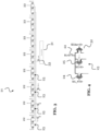
- the first multiplexer 21 of the circuit 20 is shown, which is designed for multiplexing to eight bit lines 22 (BL ⁇ o> to BL ⁇ 7>). Each bit line 11 is associated with a first select device 23.
- An enlarged view of an exemplary first select device 23 is shown in FIG. 4 .
- the first select device 23 comprises the first transistor 24 (SEL_R) and the second transistor 25 (SEL).
- the first select device 23 may further comprise a third transistor 32 (SELbar).
- the controller 26 (not shown in FIG. 3 and FIG. 4 ) is configured to turn on the third transistor 32 of the first select device 23, if at least one of the first transistor 24 and the second transistor 25 of the first select device 23 is turned on for the write operation or the read operation using the particular bit line 22 associated with the first select device 23.
- the first transistor 24 and second transistor 25 are controlled as described with respect to FIG. 2 .
- the first transistor 24 and the second transistor 25 may be NMOS transistors, and the third transistor 32 maybe a PMOS transistor as shown in FIG. 3 .
- the first transistor 24 and the second transistor 25 could be PMOS transistors, and the third transistor 32 could be an NMOS transistor.
- FIG. 3 shows further that the write-read circuit 20 may also comprise a sense amplifier 31.
- the sense amplifier 31 may be used for reading using the bit lines 22, i.e., it may sense data on the particular bit line 22 during the read operation.
- the sense amplifier 31 can be connected by a first clamp transistor 33 to the first multiplexer 21.
- the write-read circuit 20 may further comprise access transistors (denoted BL_A and BLbar_A in FIG. 3 ), in order to provide access to the first and second transistors 24, 25 of the first select devices 25, and respectively the third transistors 32 of the first select devices 23.
- the write-read circuit 20 may further comprise a write driver (not shown in FIG. 3 ), which is connected to the first multiplexer 21 and configured to drive the write operation, i.e., to provide the data to be written, using the particular bit line 22.
- FIG. 5 shows a table summarizing the solution of this disclosure.
- the disclosure proposes dividing the first multiplexer 21 into a read multiplexer part and a write multiplexer part, which is achieved by dividing each first select device 23 of the first multiplexer 21 into the first transistor 24 and the second transistor 25.
- both transistors 24, 25 (SEL_R and SEL are at 1) are turned on.
- the third transistor 32 may be turned on (SELbar is at 0, due to the opposite polarity).
- SEL_R the first transistor 24 is turned on (SEL_R at 1, SEL at 0, and SELbar at 1). This allows reducing the bit line loading during reading without increasing the periphery area.
- FIG. 6 shows another example of a write-read circuit 20 according to this disclosure, which builds on the circuit 20 shown in FIG. 3 . Same elements are labeled with the same reference signs and may function likewise.
- the circuit 20 of FIG. 6 further comprises, apart from the first multiplexer 21 already described in FIG. 3 , a second multiplexer 61 for multiplexing the write and read operations to the memory device.
- the second multiplexer 61 comprises a plurality of second select devices 63, wherein each second select device 63 is associated with one of a plurality of reference bit lines 62 of the memory device (note that in FIG. 6 only one reference bit line 62 is shown), wherein each reference bit lines 62 is related to one of the bit lines 22.
- each second select device 63 comprises a first transistor 64 and a second transistor 65.
- the second multiplexer 61 can be configured in a similar manner than the first multiplexer 23.
- the second select devices 63 may be configured in a similar manner than the first select devices 23, for instance, with respect to read current and write current, or in ratio of the transistor width (see above description for the first select devices 23).
- the controller 26 is also configured to control the second multiplexer 61.
- the controller 26 is configured to perform a write operation or a read operation using the particular bit line 22 based on using further a particular reference bit line 62 of the plurality of reference bit lines 62.
- the controller 26 is configured to turn on both transistors 64, 65 of the second select device 63 that is associated with the particular reference bit line 62.
- the controller 26 is configured to turn on the first transistor 64 and turn off the second transistor 65 of the second select device 63 that is associated with the particular reference bit line 62.
- the sense amplifier 31 may be connected by a second clamp transistor 67 to the second multiplexer 61, to which already the first multiplexer 21 is connected. Further, a write driver (not shown) maybe connected to the first multiplexer 21 and the second multiplexer 61.
- FIG. 7 shows a write-read method 70 according to this disclosure, usable for multiplexing write and read operations to a memory device.
- the method 70 may be performed using the read-write circuit 20 of FIG. 1 .
- the method 70 comprises a step 71 of performing a write operation using a particular bit line 22 of a plurality of bit lines 22 of the memory device, by turning on a first transistor 24 and a second transistor 25 of a first select device 23 of a first multiplexer 21 of the circuit 20.
- the first select device 23 is associated with the particular bit line 22.
- the method 70 further comprises a step 72 of performing a read operation using the particular bit line 22, by turning on the first transistor 24 and turning off the second transistor 25 of the first select device 21 associated with the particular bit line 22.
- a main advantage is that the read delay and the read energy are improved, i.e., they are decreased, without increasing the periphery area.
- stress on near memory cells may be reduced. Further, it may be possible to modulate the write current. For example, the reduction of the stress on the near memory cell may be reduced by turning on the read transistor(s) 24, 64 during the write operation. Secondly, the modulation of the write current may be achieved by having more current in one direction as in the other direction.
Landscapes
- Engineering & Computer Science (AREA)
- Computer Hardware Design (AREA)
- Static Random-Access Memory (AREA)
Abstract
Description
- The present disclosure relates to memory devices, in particular, to memory devices with multiplexers configured to multiplex write and read operations to bit lines. The disclosure provides a write-read circuit for such a memory device. The write-read circuit comprises at least one multiplexer for a plurality bit lines, wherein the multiplexer is configurable depending on whether a read operation or a write operation is performed using one of these bit lines.
- On-chip embedded memory devices with non-volatility, for instance, a magnetic random-access memory (MRAM) device, may enable energy and computational efficiency with a memory density exceeding that of a high-density static random-access memory (SRAM) device. These non-volatile memory devices target, for example, lower level caches, like L2-L3-L4. Reading is more crucial as writing for such lower level caches. Any improvement in reading will thus help replacing SRAM devices. The bit line capacitance is thereby a crucial parameter, which determines the read delay as well as the read energy. For example, the higher the bit line capacitance, the more read delay is experienced.
- Multiplexing in memory devices helps reducing the periphery areas and IOs. The multiplexing can be implemented using multiplexers, which connect the memory macro (which includes the memory cells and memory lines) with the write and read circuitry. The memory macro can particularly comprise spin transfer torque (STT) or spin orbit torque (SOT) memory cells (wherein both are current based memory cells).
- The write and read circuitry determines the write current and the read current, respectively. A higher write current requirement leads to larger multiplexer dimensions, which increases bit line loading. Further, the read delay and read energy increase with the higher bit line loading. A reduction of the multiplexer size (e.g., from 16:1 to 4:1), in order to decrease the bit line loading, would unfortunately increase the periphery area, and hence the leakage.
- In view of the above, an objective of this disclosure is to provide improved multiplexing of write and read operations to bit lines of a memory device. TO this end, an objective is to provide a write-read circuit with a multiplexer, which does not increase the bit line loading, in particular, not during read operations. Another objective is to avoid an increase in the periphery area and leakage, respectively.
- These and other objectives are achieved by the solutions of this disclosure provided in the independent claims. Advantageous implementations are described in the dependent claims.
- A first aspect of this disclosure is a write-read circuit for a memory device, the write-read circuit comprising a first multiplexer for multiplexing write and read operations to the memory device, wherein the first multiplexer comprises a plurality of first select devices, wherein each first select device is associated with one of a plurality of bit lines of the memory device, and wherein each first select device comprises a first transistor and a second transistor; and a controller for controlling the first multiplexer, wherein the controller is configured to: for a write operation using a particular bit line of the bit lines, turn on both transistors of the first select device that is associated with the particular bit line; and for a read operation using the particular bit line, turn on the first transistor and turn off the second transistor of the first select device that is associated with the particular bit line.
- In the write-read circuit of the first aspect, the first multiplexer maybe divided into a write part and a read part. That is, each select device of the first multiplexer may be divided into the first transistor and the second transistor, wherein the first transistor is used as a read transistor, and both the first transistor and the second transistor are used as write transistors. The transistors may, for instance, be NMOS or PMOS transistors. During the write operation, both transistors of the first select device are turned on, and during the read operation only the read transistor is turned on. This may lead to a reduction of the capacitive loading on the particular bit line when performing the read operation, event without reducing the multiplexer dimension. Thus, also the read delay and the read energy can be reduced. Further, also the periphery area does not have to be increased and likewise the leakage stay the same. During the write operation, the two turned on transistors ensure sufficient write current.
- In an implementation, the write-read circuit further comprises a second multiplexer for multiplexing the write and read operations to the memory device, wherein the second multiplexer comprises a plurality of second select devices, wherein each second select device is associated with one of a plurality of reference bit lines of the memory device, wherein each of the reference bit lines is related to one of the bit lines, and wherein each second select device comprises a first transistor and a second transistor; wherein the controller is also for controlling the second multiplexer, and is configured to: for the write operation using the particular bit line, turn on both transistors of the second select device that is associated with a particular reference bit line of the plurality of reference bit lines, which is related to the particular bit line; and for the read operation using the particular bit line, turn on the first transistor and turn off the second transistor of the second select device that is associated with the particular reference bit line.
- The second multiplexer is divided in a similar manner than the first multiplexer, into a read part and a write part, by dividing each second select device. The second multiplexer further supports the reduction of the capacitive loading on the particular bit line when performing the read operation.
- In an implementation of the write-read circuit, the first transistor of each select device has a smaller transistor width than the second transistor of that select device.
- This enables reducing the capacitive loading of the bit line when performing the read operation, and at the same time ensures sufficient write current when performing the write operation.
- In an implementation of the write-read circuit, a ratio of the transistor width of the second transistor to the transistor width of the first transistor of each select device is in a range of 5:1 to 10:1.
- This range has proven beneficial for many different implementations of the memory device, and accordingly of the write-read circuit. It may be adjusted if needed.
- In an implementation of the write-read circuit, the first transistor of each select device is configured for a read current of 10-20 µA, and the first transistor and the second transistor of each select device are together configured for a write current of 50-250 µA.
- In an implementation of the write-read circuit, each select device further comprises a third transistor, and the controller is configured to turn on the third transistor of the select device associated with the particular bit line or the particular reference bitline, if at least one of the first transistor and the second transistor of that select device is turned on for the write operation or the read operation using the particular bit line.
- The third transistor further supports the read and write operations, respectively.
- In an implementation of the write-read circuit, for each select device, the first transistor and the second transistor are NMOS transistors and the third transistor is a PMOS transistor; or the first transistor and the second transistor are PMOS transistors and the third transistor is an NMOS transistor.
- In an implementation, the write-read circuit further comprises a sense amplifier and a write driver connected, respectively, to the first multiplexer and/or the second multiplexer.
- In an implementation of the write-read circuit, the sense amplifier is connected by a first clamp transistor to the first multiplexer and by a second clamp transistor to the second multiplexer.
- A second aspect of this disclosure is a memory device comprising: a plurality of memory cells; a plurality of bit lines, wherein multiple memory cells of the plurality of memory cells are connected to each of the bit lines; and a write-read circuit according to the first aspect or any of its implementations; wherein the write operation using the particular bit line of the plurality of bit lines of the memory device is for writing into one of the memory cells connected to the particular bit line; and the read operation using the particular bit line is for reading from one of the memory cells connected to the particular bit line.
- In an implementation, the memory device further comprises a plurality of reference bit lines, wherein multiple memory cells of the plurality of memory cells are connected to each of the reference bit lines, wherein each memory cell of the memory device is connected to one of the bit lines and to one of the reference bit lines; and wherein the write operation using the particular bit line is for writing into one of the memory cells connected to the particular bit line and to the particular reference bit line; and wherein the read operation using the particular bit line for reading from one of the memory cells connected to the particular bit line and to the particular reference bit line.
- In an implementation of the memory device, each memory cell of the memory device comprises a magnetic stack, and wherein the memory device is configured to: in the write operation, pass a current through the magnetic stack or past the magnetic stack; and in the read operation, pass a current through the magnetic stack.
- In an implementation, the memory device is a MRAM device, a STT MRAM device, or a SOT MRAM device.
- The memory device of the second aspect enjoys all the advantages provided by the write-read circuit of the first aspect, which are described above.
- A third aspect of this disclosure is write-read method for multiplexing write and read operations to a memory device, the method comprising: for performing a write operation using a particular bit line of a plurality of bit lines of the memory device, turning on a first transistor and a second transistor of a first select device of a first multiplexer, wherein the first select device is associated with the particular bit line; and for performing a read operation using the particular bit line, turning on the first transistor and turning off the second transistor of the first select device associated with the particular bit line.
- In an implementation, the write-read method further comprises: for performing the write operation using the particular bit line, turning on a first transistor and a second transistor of a second select device of a second multiplexer, wherein the second select device is associated with a particular reference bit line of plurality of reference bit lines of the memory device, and wherein the particular reference bit line is related to the particular bit line; and for performing the read operation using the particular bit line, turning on the first transistor and turning off the second transistor of the second select device that is associated with the particular reference bit line.
- The method of the third aspect achieves the same advantages as the write-read circuit of the first aspect, and may be extended by respective implementations as described above for the write-read circuit of the first aspect.
- The above described aspects and implementations are explained in the following description of embodiments with respect to the enclosed drawings:
- FIG. 1
- shows an exemplary write-read circuit for multiplexing write and read operations using bit lines of a memory device.
- FIG. 2
- shows a write-read circuit according to this disclosure.
- FIG. 3
- shows an example of a write-read circuit according to this disclosure, for multiplexing write and read operations using bit lines of a memory device.
- FIG. 4
- shows an example of a select device associated with a bit line.
- FIG. 5
- shows a table indicating an operation of a select device for writing to and reading from a bit line, respectively.
- FIG. 6
- shows an example of a write-read circuit according to this disclosure, for multiplexing write and read operations using bit lines of a memory device.
- FIG. 7
- shows a method according to this disclosure for operating a writeread circuit.
-
FIG. 1 shows a conventional read-write circuit 10. The exemplary circuit 10 comprises a multiplexer for multiplexing write and read operations using a plurality of bit lines 12. The multiplexer comprises aselect device 11 for eachbit line 12. Each of theselect devices 11 comprises at least onetransistor 13, or as shown inFIG. 1 may comprise twotransistors transistors - For the read-circuit 10 of
FIG. 1 , independent of whether a write operation or a read operation is performed using aparticular bit line 12, bothtransistors select device 11, which is associated with theparticular bit line 12, are turned on (i.e., are activated). - However, for instance, STT and SOT memory devices are current based memory devices. A STT switching (write) current is, for example, more than 100 µA, and a SOT switching (write) current is even more than 200 µA. In contrast, a read current can be 20 µA for STT, and can be between 30-40 µA for SOT. That is, the read current is almost 5-6 times less than the write current. That means, that the
transistors - The high write current requirement leads to high multiplexed dimensions (e.g., 16:1), which increases loading on the bit lines. The large bit line loading is a problem during the read operation. In particular, the read delay and the read energy increase with higher bit line loading. However, if one were to simply decrease the multiplexer dimension (e.g., from 16:1 to 4:1), this would reduce the bit line loading, but would increase the periphery area and hence the leakage.
- In order to decrease the read delay and read energy without increasing the periphery area and leakage, this disclosure proposes a write-
read circuit 20 for a memory device, as shown inFIG. 2 . The write-read circuit 20 is particularly useful if the memory device is a MRAM device, a STT memory device, or a SOT memory device. In such memory devices, each memory cell of the memory device may comprises a magnetic stack, and a write operation to a memory cell passes a current through the magnetic stack or passes a current past the magnetic stack, and a read operation from the memory cell passes a current through the magnetic stack. - The write-
read circuit 20 ofFIG. 2 comprises at least one multiplexer, particularly comprises afirst multiplexer 21 for multiplexing write and read access tobit lines 22 of the memory device. Thefirst multiplexer 21 comprises a plurality of firstselect devices 23. Each of the firstselect devices 23 is associated with one of a plurality ofbit lines 22 of the memory device, and may control access to thatbit line 22, in order to perform a write operation or a read operation using thatbit line 22. The write or read operation using thatbit line 22 may write data into a memory cell, or may read data from a memory cell, connected to thatbit line 22. - Each of the first
select devices 23 comprises afirst transistor 24 and asecond transistor 25, which may be referred to as select or access transistors. If aparticular bit line 22 is to be used for the write operation or the read operation, one or both of thetransistors particular bit line 22, as described below. - The write-
read circuit 20 comprises acontroller 26 configured to control thefirst multiplexer 21. Thecontroller 26 is configured to control the write-read circuit 20 to perform the write operation or the read operation using theparticular bit line 22. For the write operation using theparticular bit line 22, the controller is configured to turn on bothtransistors select device 23, which is associated with theparticular bit line 22. For the read operation using theparticular bit line 22, thecontroller 26 is configured to turn on thefirst transistor 24 and to turn off thesecond transistor 25 of the firstselect device 23, which is associated with theparticular bit line 22. - Since for the read operation only the first transistor 24 (read transistor) is turned on, the
first transistor 24 can be made smaller, due to the lower read current requirement, which allows decreasing the capacitive loading of theparticular bit line 22 during the read operation, and thus reducing the read delay and read energy. For the write operation, by also turning on thesecond transistor 25, the higher write current requirement can be met. For example, thefirst transistor 24 may be configured for a read current of 10-20 µA, and the first andsecond transistor second transistor 25 to the transistor width of thefirst transistor 24 being in a range of 5:1 to 10:1. -
FIG. 3 shows an example of the write-read circuit 20 according to this disclosure, which builds on thecircuit 20 shown inFIG. 1 . Same elements are labelled with the same reference signs and may function likewise. - In
FIG. 3 , thefirst multiplexer 21 of thecircuit 20 is shown, which is designed for multiplexing to eight bit lines 22 (BL<o> to BL<7>). Eachbit line 11 is associated with a firstselect device 23. An enlarged view of an exemplary firstselect device 23 is shown inFIG. 4 . The firstselect device 23 comprises the first transistor 24 (SEL_R) and the second transistor 25 (SEL). As also shown inFIG. 3 , the firstselect device 23 may further comprise a third transistor 32 (SELbar). - The controller 26 (not shown in
FIG. 3 and FIG. 4 ) is configured to turn on thethird transistor 32 of the firstselect device 23, if at least one of thefirst transistor 24 and thesecond transistor 25 of the firstselect device 23 is turned on for the write operation or the read operation using theparticular bit line 22 associated with the firstselect device 23. Thefirst transistor 24 andsecond transistor 25 are controlled as described with respect toFIG. 2 . - The
first transistor 24 and thesecond transistor 25 may be NMOS transistors, and thethird transistor 32 maybe a PMOS transistor as shown inFIG. 3 . Alternatively, thefirst transistor 24 and thesecond transistor 25 could be PMOS transistors, and thethird transistor 32 could be an NMOS transistor. -
FIG. 3 shows further that the write-read circuit 20 may also comprise asense amplifier 31. Thesense amplifier 31 may be used for reading using the bit lines 22, i.e., it may sense data on theparticular bit line 22 during the read operation. Thesense amplifier 31 can be connected by afirst clamp transistor 33 to thefirst multiplexer 21. - The write-
read circuit 20 may further comprise access transistors (denoted BL_A and BLbar_A inFIG. 3 ), in order to provide access to the first andsecond transistors select devices 25, and respectively thethird transistors 32 of the firstselect devices 23. The write-read circuit 20 may further comprise a write driver (not shown inFIG. 3 ), which is connected to thefirst multiplexer 21 and configured to drive the write operation, i.e., to provide the data to be written, using theparticular bit line 22. -
FIG. 5 shows a table summarizing the solution of this disclosure. The disclosure proposes dividing thefirst multiplexer 21 into a read multiplexer part and a write multiplexer part, which is achieved by dividing each firstselect device 23 of thefirst multiplexer 21 into thefirst transistor 24 and thesecond transistor 25. During the write operation, bothtransistors 24, 25 (SEL_R and SEL are at 1) are turned on. Also thethird transistor 32 may be turned on (SELbar is at 0, due to the opposite polarity). During the read operation, only thefirst transistor 24 is turned on (SEL_R at 1, SEL at 0, and SELbar at 1). This allows reducing the bit line loading during reading without increasing the periphery area. -
FIG. 6 shows another example of a write-read circuit 20 according to this disclosure, which builds on thecircuit 20 shown inFIG. 3 . Same elements are labeled with the same reference signs and may function likewise. - The
circuit 20 ofFIG. 6 further comprises, apart from thefirst multiplexer 21 already described inFIG. 3 , asecond multiplexer 61 for multiplexing the write and read operations to the memory device. Thesecond multiplexer 61 comprises a plurality of secondselect devices 63, wherein each secondselect device 63 is associated with one of a plurality ofreference bit lines 62 of the memory device (note that inFIG. 6 only onereference bit line 62 is shown), wherein each reference bit lines 62 is related to one of the bit lines 22. Further, each secondselect device 63 comprises afirst transistor 64 and asecond transistor 65. Generally, thesecond multiplexer 61 can be configured in a similar manner than thefirst multiplexer 23. For instance, the secondselect devices 63 may be configured in a similar manner than the firstselect devices 23, for instance, with respect to read current and write current, or in ratio of the transistor width (see above description for the first select devices 23). - The
controller 26 is also configured to control thesecond multiplexer 61. In particular thecontroller 26 is configured to perform a write operation or a read operation using theparticular bit line 22 based on using further a particularreference bit line 62 of the plurality of reference bit lines 62. For the write operation using theparticular bit line 22, thecontroller 26 is configured to turn on bothtransistors select device 63 that is associated with the particularreference bit line 62. For the read operation using theparticular bit line 22, thecontroller 26 is configured to turn on thefirst transistor 64 and turn off thesecond transistor 65 of the secondselect device 63 that is associated with the particularreference bit line 62. - As shown further in
FIG. 6 , thesense amplifier 31 may be connected by asecond clamp transistor 67 to thesecond multiplexer 61, to which already thefirst multiplexer 21 is connected. Further, a write driver (not shown) maybe connected to thefirst multiplexer 21 and thesecond multiplexer 61. -
FIG. 7 shows a write-read method 70 according to this disclosure, usable for multiplexing write and read operations to a memory device. Themethod 70 may be performed using the read-write circuit 20 ofFIG. 1 . - The
method 70 comprises astep 71 of performing a write operation using aparticular bit line 22 of a plurality ofbit lines 22 of the memory device, by turning on afirst transistor 24 and asecond transistor 25 of a firstselect device 23 of afirst multiplexer 21 of thecircuit 20. The firstselect device 23 is associated with theparticular bit line 22. Themethod 70 further comprises astep 72 of performing a read operation using theparticular bit line 22, by turning on thefirst transistor 24 and turning off thesecond transistor 25 of the firstselect device 21 associated with theparticular bit line 22. - The solutions of this disclosure, including the write-
read circuit 20 and the write-read method 70, provide several advantages. A main advantage is that the read delay and the read energy are improved, i.e., they are decreased, without increasing the periphery area. - In addition, stress on near memory cells may be reduced. Further, it may be possible to modulate the write current. For example, the reduction of the stress on the near memory cell may be reduced by turning on the read transistor(s) 24, 64 during the write operation. Secondly, the modulation of the write current may be achieved by having more current in one direction as in the other direction.
- In the claims as well as in the description of this disclosure, the word "comprising" does not exclude other elements or steps and the indefinite article "a" or "an" does not exclude a plurality. A single element may fulfill the functions of several entities or items recited in the claims. The mere fact that certain measures are recited in the mutual different dependent claims does not indicate that a combination of these measures cannot be used in an advantageous implementation.
Claims (15)
- A write-read circuit (20) for a memory device, the write-read circuit (20) comprisinga first multiplexer (21) for multiplexing write and read operations to the memory device,wherein the first multiplexer (21) comprises a plurality of first select devices (23), wherein each first select device (23) is associated with one of a plurality of bit lines (22) of the memory device, and wherein each first select device (23) comprises a first transistor (24) and a second transistor (25); anda controller (26) for controlling the first multiplexer (21), wherein the controller (26) is configured to:for a write operation using a particular bit line (22) of the bit lines (22), turn on both transistors (24, 25) of the first select device (23) that is associated with the particular bit line (22); andfor a read operation using the particular bit line (22), turn on the first transistor (24) and turn off the second transistor (25) of the first select device (23) that is associated with the particular bit line (22).
- The write-read circuit (20) according to claim 1, further comprisinga second multiplexer (61) for multiplexing the write and read operations to the memory device,wherein the second multiplexer (61) comprises a plurality of second select devices (63), wherein each second select device (63) is associated with one of a plurality of reference bit lines (62) of the memory device, wherein each of the reference bit lines (62) is related to one of the bit lines (22), and wherein each second select device (63) comprises a first transistor (64) and a second transistor (65);wherein the controller (26) is also for controlling the second multiplexer (61), and is configured to:for the write operation using the particular bit line (22), turn on both transistors (64, 65) of the second select device (63) that is associated with a particular reference bit line (62) of the plurality of reference bit lines (62), which is related to the particular bit line (22); andfor the read operation using the particular bit line (22), turn on the first transistor (64) and turn off the second transistor (65) of the second select device (63) that is associated with the particular reference bit line (62).
- The write-read circuit (20) according to claim 1 or 2, wherein the first transistor (24, 64) of each select device (23, 63) has a smaller transistor width than the second transistor (25, 65) of that select device (23, 63).
- The write-read circuit (20) according to claim 3, wherein a ratio of the transistor width of the second transistor (25, 65) to the transistor width of the first transistor (24, 64) of each select device (23, 63) is in a range of 5:1 to 10:1.
- The write-read circuit (20) according to one of the claims 1 to 4, wherein the first transistor (24, 64) of each select device (23, 63) is configured for a read current of 10-20 µA, and the first transistor (24, 64) and the second transistor (25, 65) of each select device (23, 63) are together configured for a write current of 50-250 µA.
- The write-read circuit (20) according to one of the claims 1 to 5, wherein each select device (23, 63) further comprises a third transistor (32, 66), and the controller (26) is configured to:
turn on the third transistor (32, 66) of the select device (23, 63) associated with the particular bit line (22) or the particular reference bit line (62), if at least one of the first transistor (24, 64) and the second transistor (25, 65) of that select device (23, 63) is turned on for the write operation or the read operation using the particular bit line (22). - The write-read circuit (20) according to claim 6, wherein, for each select device (23, 63),the first transistor (24, 64) and the second transistor (25, 65) are NMOS transistors and the third transistor (32, 66) is a PMOS transistor; orthe first transistor (24, 64) and the second transistor (25, 65) are PMOS transistors and the third transistor (32, 66) is an NMOS transistor.
- The write-read circuit (20) according to one of the claims 1 to 7, further comprising a sense amplifier (31) and a write driver connected, respectively, to the first multiplexer (21) and/or the second multiplexer (61).
- The write-read circuit (20) according to claim 8, wherein the sense amplifier (31) is connected by a first clamp transistor (33) to the first multiplexer (21) and by a second clamp transistor (67) to the second multiplexer (61).
- A memory device comprising:a plurality of memory cells;a plurality of bit lines (22), wherein multiple memory cells of the plurality of memory cells are connected to each of the bit lines (22); anda write-read circuit (20) according to one of the claims 1 to 8;wherein the write operation using the particular bit line (22) of the plurality of bit lines (22) of the memory device is for writing into one of the memory cells connected to the particular bit line (22); andthe read operation using the particular bit line (22) is for reading from one of the memory cells connected to the particular bit line (22).
- The memory device according to claim 9, further comprisinga plurality of reference bit lines (62), wherein multiple memory cells of the plurality of memory cells are connected to each of the reference bit lines (62), wherein each memory cell of the memory device is connected to one of the bit lines (22) and to one of the reference bit lines (62); andwherein the write operation using the particular bit line (22) is for writing into one of the memory cells connected to the particular bit line (22) and to the particular reference bit line (62); andwherein the read operation using the particular bit line (22) for reading from one of the memory cells connected to the particular bit line (22) and to the particular reference bit line (62).
- The memory device according to claim 9 or 10, wherein each memory cell of the memory device comprises a magnetic stack, and wherein the memory device is configured to:in the write operation, pass a current through the magnetic stack or past the magnetic stack; andin the read operation, pass a current through the magnetic stack.
- The memory device according to one of the claims 9 to 11, wherein the memory device is a magnetic random access memory, MRAM, device, a spin-transfer torque STT, MRAM device, or a spin-orbit torque, SOT, MRAM device.
- A write-read method (70) for multiplexing write and read operations to a memory device, the method (70) comprising:for performing (71) a write operation using a particular bit line (22) of a plurality of bit lines (22) of the memory device, turning on a first transistor (24) and a second transistor (25) of a first select device (23) of a first multiplexer (21), wherein the first select device (23) is associated with the particular bit line (22); andfor performing (72) a read operation using the particular bit line (22), turning on the first transistor (24) and turning off the second transistor (25) of the first select device (21) associated with the particular bit line (22).
- The write-read method (70) according to claim 14, further comprisingfor performing (71) the write operation using the particular bit line (22), turning on a first transistor (64) and a second transistor (65) of a second select device (63) of a second multiplexer (61), wherein the second select device (63) is associated with a particular reference bit line (62) of plurality of reference bit lines (62) of the memory device, and wherein the particular reference bit line (62) is related to the particular bit line (22); andfor performing (72) the read operation using the particular bit line (22), turning on the first transistor (64) and turning off the second transistor (65) of the second select device (63) that is associated with the particular reference bit line (62).
Priority Applications (2)
| Application Number | Priority Date | Filing Date | Title |
|---|---|---|---|
| EP22208698.5A EP4376007B1 (en) | 2022-11-22 | 2022-11-22 | A write-read circuit with a bit line multiplexer for a memory device |
| US18/514,100 US12531100B2 (en) | 2022-11-22 | 2023-11-20 | Write-read circuit with a bit line multiplexer for a memory device |
Applications Claiming Priority (1)
| Application Number | Priority Date | Filing Date | Title |
|---|---|---|---|
| EP22208698.5A EP4376007B1 (en) | 2022-11-22 | 2022-11-22 | A write-read circuit with a bit line multiplexer for a memory device |
Publications (2)
| Publication Number | Publication Date |
|---|---|
| EP4376007A1 true EP4376007A1 (en) | 2024-05-29 |
| EP4376007B1 EP4376007B1 (en) | 2026-03-11 |
Family
ID=84360970
Family Applications (1)
| Application Number | Title | Priority Date | Filing Date |
|---|---|---|---|
| EP22208698.5A Active EP4376007B1 (en) | 2022-11-22 | 2022-11-22 | A write-read circuit with a bit line multiplexer for a memory device |
Country Status (2)
| Country | Link |
|---|---|
| US (1) | US12531100B2 (en) |
| EP (1) | EP4376007B1 (en) |
Citations (4)
| Publication number | Priority date | Publication date | Assignee | Title |
|---|---|---|---|---|
| US20020093032A1 (en) * | 2000-11-27 | 2002-07-18 | Satoru Hanzawa | Semiconductor device |
| US20100091581A1 (en) * | 2008-10-14 | 2010-04-15 | Arm Limited | Memory device and method of operating such a memory device |
| US20170309330A1 (en) * | 2016-04-21 | 2017-10-26 | Suk-Soo Pyo | Resistive memory device and a memory system including the same |
| US20190108872A1 (en) * | 2017-10-06 | 2019-04-11 | Qualcomm Incorporated | Area efficient write data path circuit for sram yield enhancement |
Family Cites Families (5)
| Publication number | Priority date | Publication date | Assignee | Title |
|---|---|---|---|---|
| KR20170090293A (en) * | 2016-01-28 | 2017-08-07 | 삼성전자주식회사 | Memory Device Having Separate Source Line Structure |
| US11586882B2 (en) * | 2018-01-24 | 2023-02-21 | International Business Machines Corporation | Synapse memory |
| JP2019160368A (en) * | 2018-03-13 | 2019-09-19 | 東芝メモリ株式会社 | Semiconductor storage device |
| US10446213B1 (en) * | 2018-05-16 | 2019-10-15 | Everspin Technologies, Inc. | Bitline control in differential magnetic memory |
| US11996145B2 (en) * | 2022-05-03 | 2024-05-28 | Western Digital Technologies, Inc. | Cross-point array with threshold switching selector memory element |
-
2022
- 2022-11-22 EP EP22208698.5A patent/EP4376007B1/en active Active
-
2023
- 2023-11-20 US US18/514,100 patent/US12531100B2/en active Active
Patent Citations (4)
| Publication number | Priority date | Publication date | Assignee | Title |
|---|---|---|---|---|
| US20020093032A1 (en) * | 2000-11-27 | 2002-07-18 | Satoru Hanzawa | Semiconductor device |
| US20100091581A1 (en) * | 2008-10-14 | 2010-04-15 | Arm Limited | Memory device and method of operating such a memory device |
| US20170309330A1 (en) * | 2016-04-21 | 2017-10-26 | Suk-Soo Pyo | Resistive memory device and a memory system including the same |
| US20190108872A1 (en) * | 2017-10-06 | 2019-04-11 | Qualcomm Incorporated | Area efficient write data path circuit for sram yield enhancement |
Also Published As
| Publication number | Publication date |
|---|---|
| US12531100B2 (en) | 2026-01-20 |
| US20240170034A1 (en) | 2024-05-23 |
| EP4376007B1 (en) | 2026-03-11 |
Similar Documents
| Publication | Publication Date | Title |
|---|---|---|
| KR102755864B1 (en) | Method for providing device status in response to a read command directed to a write-only mode register bit, and memory device and system using the same | |
| JP5197448B2 (en) | Resistance change memory device | |
| JP2021168225A (en) | Data caching | |
| TWI321796B (en) | Word-line driver | |
| EP2988305B1 (en) | Integrated circuit for storing data | |
| US9606743B2 (en) | Semiconductor memory device and driving method of the same | |
| US10431277B2 (en) | Memory device | |
| JP2013089279A (en) | Resistive memory apparatus, layout structure thereof, and sensing circuit | |
| US10210932B2 (en) | Electronic device with semiconductor memory having variable resistance elements for storing data and associated driving circuitry | |
| CN107689235A (en) | non-volatile memory | |
| US20170178706A1 (en) | Nonvolatile semiconductor memory | |
| JP2011258288A (en) | Semiconductor memory device | |
| KR20150120557A (en) | Electronic device including semiconductor memory and operation method of the same | |
| JP2018005962A (en) | Nonvolatile semiconductor storage device | |
| EP1665275B1 (en) | Method and apparatus for read bitline clamping for gain cell dram devices | |
| US20050276100A1 (en) | Method and system for optimizing the number of word line segments in a segmented MRAM array | |
| JP2006019005A (en) | Random access memory array with parity bit structure | |
| EP4250295A1 (en) | Persistent xspi stt-mram with optional erase operation | |
| EP4376007B1 (en) | A write-read circuit with a bit line multiplexer for a memory device | |
| US20170221574A1 (en) | Fuse memory having discharge circuit | |
| US11664081B2 (en) | Bit selection for power reduction in stacking structure during memory programming | |
| US7460400B1 (en) | Nonvolatile memory utilizing MIS memory transistors with bit mask function | |
| EP3826017B1 (en) | Non-volatile sram device | |
| KR100276009B1 (en) | Semiconductor memory device with efficient layout | |
| RU2634217C2 (en) | Semiconductor memory device |
Legal Events
| Date | Code | Title | Description |
|---|---|---|---|
| PUAI | Public reference made under article 153(3) epc to a published international application that has entered the european phase |
Free format text: ORIGINAL CODE: 0009012 |
|
| STAA | Information on the status of an ep patent application or granted ep patent |
Free format text: STATUS: THE APPLICATION HAS BEEN PUBLISHED |
|
| AK | Designated contracting states |
Kind code of ref document: A1 Designated state(s): AL AT BE BG CH CY CZ DE DK EE ES FI FR GB GR HR HU IE IS IT LI LT LU LV MC ME MK MT NL NO PL PT RO RS SE SI SK SM TR |
|
| STAA | Information on the status of an ep patent application or granted ep patent |
Free format text: STATUS: REQUEST FOR EXAMINATION WAS MADE |
|
| 17P | Request for examination filed |
Effective date: 20241121 |
|
| RBV | Designated contracting states (corrected) |
Designated state(s): AL AT BE BG CH CY CZ DE DK EE ES FI FR GB GR HR HU IE IS IT LI LT LU LV MC ME MK MT NL NO PL PT RO RS SE SI SK SM TR |
|
| GRAP | Despatch of communication of intention to grant a patent |
Free format text: ORIGINAL CODE: EPIDOSNIGR1 |
|
| STAA | Information on the status of an ep patent application or granted ep patent |
Free format text: STATUS: GRANT OF PATENT IS INTENDED |
|
| RIC1 | Information provided on ipc code assigned before grant |
Ipc: G11C 11/16 20060101AFI20251006BHEP Ipc: G11C 5/06 20060101ALN20251006BHEP Ipc: G11C 7/12 20060101ALN20251006BHEP |
|
| INTG | Intention to grant announced |
Effective date: 20251029 |
|
| GRAS | Grant fee paid |
Free format text: ORIGINAL CODE: EPIDOSNIGR3 |
|
| GRAA | (expected) grant |
Free format text: ORIGINAL CODE: 0009210 |
|
| STAA | Information on the status of an ep patent application or granted ep patent |
Free format text: STATUS: THE PATENT HAS BEEN GRANTED |
|
| AK | Designated contracting states |
Kind code of ref document: B1 Designated state(s): AL AT BE BG CH CY CZ DE DK EE ES FI FR GB GR HR HU IE IS IT LI LT LU LV MC ME MK MT NL NO PL PT RO RS SE SI SK SM TR |
|
| REG | Reference to a national code |
Ref country code: CH Ref legal event code: F10 Free format text: ST27 STATUS EVENT CODE: U-0-0-F10-F00 (AS PROVIDED BY THE NATIONAL OFFICE) Effective date: 20260311 Ref country code: GB Ref legal event code: FG4D |
|
| REG | Reference to a national code |
Ref country code: DE Ref legal event code: R096 Ref document number: 602022032038 Country of ref document: DE |
|
| REG | Reference to a national code |
Ref country code: IE Ref legal event code: FG4D |
|
| PG25 | Lapsed in a contracting state [announced via postgrant information from national office to epo] |
Ref country code: RS Free format text: LAPSE BECAUSE OF FAILURE TO SUBMIT A TRANSLATION OF THE DESCRIPTION OR TO PAY THE FEE WITHIN THE PRESCRIBED TIME-LIMIT Effective date: 20260611 |
|
| PG25 | Lapsed in a contracting state [announced via postgrant information from national office to epo] |
Ref country code: ES Free format text: LAPSE BECAUSE OF FAILURE TO SUBMIT A TRANSLATION OF THE DESCRIPTION OR TO PAY THE FEE WITHIN THE PRESCRIBED TIME-LIMIT Effective date: 20260311 |
|
| PG25 | Lapsed in a contracting state [announced via postgrant information from national office to epo] |
Ref country code: GR Free format text: LAPSE BECAUSE OF FAILURE TO SUBMIT A TRANSLATION OF THE DESCRIPTION OR TO PAY THE FEE WITHIN THE PRESCRIBED TIME-LIMIT Effective date: 20260612 |
|
| REG | Reference to a national code |
Ref country code: LT Ref legal event code: MG9D |
|
| PG25 | Lapsed in a contracting state [announced via postgrant information from national office to epo] |
Ref country code: LT Free format text: LAPSE BECAUSE OF FAILURE TO SUBMIT A TRANSLATION OF THE DESCRIPTION OR TO PAY THE FEE WITHIN THE PRESCRIBED TIME-LIMIT Effective date: 20260311 |
|
| PG25 | Lapsed in a contracting state [announced via postgrant information from national office to epo] |
Ref country code: NO Free format text: LAPSE BECAUSE OF FAILURE TO SUBMIT A TRANSLATION OF THE DESCRIPTION OR TO PAY THE FEE WITHIN THE PRESCRIBED TIME-LIMIT Effective date: 20260611 |
|
| PG25 | Lapsed in a contracting state [announced via postgrant information from national office to epo] |
Ref country code: FI Free format text: LAPSE BECAUSE OF FAILURE TO SUBMIT A TRANSLATION OF THE DESCRIPTION OR TO PAY THE FEE WITHIN THE PRESCRIBED TIME-LIMIT Effective date: 20260311 Ref country code: SE Free format text: LAPSE BECAUSE OF FAILURE TO SUBMIT A TRANSLATION OF THE DESCRIPTION OR TO PAY THE FEE WITHIN THE PRESCRIBED TIME-LIMIT Effective date: 20260311 |
|
| REG | Reference to a national code |
Ref country code: NL Ref legal event code: MP Effective date: 20260311 |
|
| PG25 | Lapsed in a contracting state [announced via postgrant information from national office to epo] |
Ref country code: HR Free format text: LAPSE BECAUSE OF FAILURE TO SUBMIT A TRANSLATION OF THE DESCRIPTION OR TO PAY THE FEE WITHIN THE PRESCRIBED TIME-LIMIT Effective date: 20260311 |
|
| PG25 | Lapsed in a contracting state [announced via postgrant information from national office to epo] |
Ref country code: LV Free format text: LAPSE BECAUSE OF FAILURE TO SUBMIT A TRANSLATION OF THE DESCRIPTION OR TO PAY THE FEE WITHIN THE PRESCRIBED TIME-LIMIT Effective date: 20260311 |
|
| PG25 | Lapsed in a contracting state [announced via postgrant information from national office to epo] |
Ref country code: BG Free format text: LAPSE BECAUSE OF FAILURE TO SUBMIT A TRANSLATION OF THE DESCRIPTION OR TO PAY THE FEE WITHIN THE PRESCRIBED TIME-LIMIT Effective date: 20260311 |