EP4375788A2 - Band gap reference circuit under low supply voltage - Google Patents
Band gap reference circuit under low supply voltage Download PDFInfo
- Publication number
- EP4375788A2 EP4375788A2 EP23212179.8A EP23212179A EP4375788A2 EP 4375788 A2 EP4375788 A2 EP 4375788A2 EP 23212179 A EP23212179 A EP 23212179A EP 4375788 A2 EP4375788 A2 EP 4375788A2
- Authority
- EP
- European Patent Office
- Prior art keywords
- voltage
- node
- mos transistor
- terminal connected
- terminal
- Prior art date
- Legal status (The legal status is an assumption and is not a legal conclusion. Google has not performed a legal analysis and makes no representation as to the accuracy of the status listed.)
- Pending
Links
Images


Classifications
-
- G—PHYSICS
- G05—CONTROLLING; REGULATING
- G05F—SYSTEMS FOR REGULATING ELECTRIC OR MAGNETIC VARIABLES
- G05F3/00—Non-retroactive systems for regulating electric variables by using an uncontrolled element, or an uncontrolled combination of elements, such element or such combination having self-regulating properties
- G05F3/02—Regulating voltage or current
- G05F3/08—Regulating voltage or current wherein the variable is DC
- G05F3/10—Regulating voltage or current wherein the variable is DC using uncontrolled devices with non-linear characteristics
- G05F3/16—Regulating voltage or current wherein the variable is DC using uncontrolled devices with non-linear characteristics being semiconductor devices
- G05F3/20—Regulating voltage or current wherein the variable is DC using uncontrolled devices with non-linear characteristics being semiconductor devices using diode- transistor combinations
-
- G—PHYSICS
- G05—CONTROLLING; REGULATING
- G05F—SYSTEMS FOR REGULATING ELECTRIC OR MAGNETIC VARIABLES
- G05F1/00—Automatic systems in which deviations of an electric quantity from one or more predetermined values are detected at the output of the system and fed back to a device within the system to restore the detected quantity to its predetermined value or values, i.e. retroactive systems
- G05F1/10—Regulating voltage or current
- G05F1/46—Regulating voltage or current wherein the variable actually regulated by the final control device is DC
- G05F1/468—Regulating voltage or current wherein the variable actually regulated by the final control device is DC characterised by reference voltage circuitry, e.g. soft start, remote shutdown
-
- G—PHYSICS
- G05—CONTROLLING; REGULATING
- G05F—SYSTEMS FOR REGULATING ELECTRIC OR MAGNETIC VARIABLES
- G05F3/00—Non-retroactive systems for regulating electric variables by using an uncontrolled element, or an uncontrolled combination of elements, such element or such combination having self-regulating properties
- G05F3/02—Regulating voltage or current
- G05F3/08—Regulating voltage or current wherein the variable is DC
- G05F3/10—Regulating voltage or current wherein the variable is DC using uncontrolled devices with non-linear characteristics
- G05F3/16—Regulating voltage or current wherein the variable is DC using uncontrolled devices with non-linear characteristics being semiconductor devices
- G05F3/20—Regulating voltage or current wherein the variable is DC using uncontrolled devices with non-linear characteristics being semiconductor devices using diode- transistor combinations
- G05F3/30—Regulators using the difference between the base-emitter voltages of two bipolar transistors operating at different current densities
-
- H—ELECTRICITY
- H03—ELECTRONIC CIRCUITRY
- H03F—AMPLIFIERS
- H03F1/00—Details of amplifiers with only discharge tubes, only semiconductor devices or only unspecified devices as amplifying elements
- H03F1/08—Modifications of amplifiers to reduce detrimental influences of internal impedances of amplifying elements
- H03F1/083—Modifications of amplifiers to reduce detrimental influences of internal impedances of amplifying elements in transistor amplifiers
- H03F1/086—Modifications of amplifiers to reduce detrimental influences of internal impedances of amplifying elements in transistor amplifiers with FET's
-
- H—ELECTRICITY
- H03—ELECTRONIC CIRCUITRY
- H03F—AMPLIFIERS
- H03F3/00—Amplifiers with only discharge tubes or only semiconductor devices as amplifying elements
- H03F3/34—DC amplifiers in which all stages are DC-coupled
- H03F3/343—DC amplifiers in which all stages are DC-coupled with semiconductor devices only
- H03F3/345—DC amplifiers in which all stages are DC-coupled with semiconductor devices only with field-effect devices
-
- H—ELECTRICITY
- H03—ELECTRONIC CIRCUITRY
- H03F—AMPLIFIERS
- H03F2200/00—Indexing scheme relating to amplifiers
- H03F2200/91—Indexing scheme relating to amplifiers the amplifier has a current mode topology
Definitions
- the present disclosure relates to a band gap reference circuit, and more particularly, to a band gap reference circuit under a low supply voltage capable of generating a band gap reference voltage in a semiconductor device having a low level of an operating voltage.
- Semiconductor devices include various circuits for generating, processing, and storing data. Such semiconductor devices receive voltages having various voltage levels from an external power source or operate using a voltage (hereinafter, referred to as a reference voltage) generated inside a circuit. Since a reference voltage generation circuit that generates a voltage having a specific voltage level includes an element with electrical characteristics varying depending on the temperature of a semiconductor device, the level of a reference voltage generated varies depending on the temperature of a corresponding semiconductor device even in a reference voltage generation circuit implemented in the same semiconductor.
- Circuits implemented in a semiconductor device operate according to a reference voltage supplied, and when the voltage level of a band gap reference voltage varies, output values of the circuits also vary, which is not what a circuit designer wants.
- a band gap reference circuit that generates a band gap reference voltage is used.
- the band gap reference circuit is a circuit that generates a band gap reference voltage insensitive to changes in the temperature of the semiconductor device by using a band gap of silicon being a material of the semiconductor device.
- the band gap refers to an energy region where a charge state density between a valence band and a conduction band is zero in a semiconductor and an insulator and the energy difference, and the electrical conductivity of a material is determined by the size of the band gap.
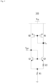
- FIG. 1 is a diagram illustrating an example of a band gap reference circuit 100 in the related art.
- the band gap reference circuit 100 in the related art generates a band gap reference voltage V REF insensitive to temperature changes by using two bipolar transistors Q1 and Q2 having different areas so that a component proportional to changes in absolute temperature (proportional to absolute temperature (PTAT)) and a component inversely proportional to changes in absolute temperature (complementary to absolute temperature (CTAT)) are offset to each other.
- PTAT proportional to absolute temperature
- CTAT complementary to absolute temperature
- the voltage level of a reference voltage used in the circuit is closely related to the power consumption of the circuit. For example, it can be easily expected that the power consumption of a circuit operating between 5 V (volts) and a ground voltage GND is greater than the power consumption of a circuit operating between 3 V and a ground voltage. Recently, in order to minimize the power consumption of a semiconductor device, the voltage level of a supply voltage of the semiconductor device tends to be reduced.
- a metal oxide silicon transistor M4 in which a source terminal is connected to a power supply voltage V DD and gate and drain terminals are diode connected to be connected to the bipolar transistor Q2, may limit the operating voltage range of the bipolar transistor Q2 by a difference voltage V DD -V D between the power supply voltage V DD and a voltage V D of the drain terminal.
- One object of the present disclosure is directed to providing a band gap reference circuit under a low supply voltage capable of generating a band gap reference voltage even under a low supply voltage by using a plurality of bias voltages separately generated and a current source using these bias voltages without using a diode connected structure used in the related art while not being affected by limitations in the operating voltage of a bipolar transistor.
- a band gap reference circuit e.g. a band gap reference circuit under a low supply voltage
- a band gap reference circuit includes: a voltage reference main circuit configured to generate a first node voltage and a second node voltage in response to a first bias voltage and a band gap reference voltage; and a transimpedance amplifier configured to generate the band gap reference voltage by amplifying a difference between the first node voltage and the second node voltage using the first bias voltage, a second bias voltage, and a third bias voltage.
- a band gap reference circuit e.g. a band gap reference circuit under a low supply voltage
- the band gap reference circuit may include one or more of the following preferred features:
- the voltage reference main circuit may comprise a first MOS transistor including one terminal connected to a power supply voltage, another terminal connected to a first node that generates the first node voltage, and a gate terminal to which the first bias voltage is applied.
- the voltage reference main circuit may comprise a second MOS transistor including one terminal connected to the power supply voltage, another terminal connected to a second node that generates the second node voltage, and a gate terminal to which the first bias voltage is applied.
- the voltage reference main circuit may comprise a first bipolar transistor including one terminal connected to the first node and a base terminal to which the band gap reference voltage is applied.
- the voltage reference main circuit may comprise a second bipolar transistor including one terminal connected to the second node, another terminal connected to a ground voltage, and a base terminal to which the band gap reference voltage is applied.
- the voltage reference main circuit may comprise a first resistor including one terminal connected to another terminal of the first bipolar transistor and the other terminal connected to the ground voltage; and/or a second resistor including one terminal commonly connected to the other terminal of the first resistor and another terminal of the second bipolar transistor, and the other terminal connected to the ground voltage.
- the transimpedance amplifier may comprise a bias stage configured to generate a fourth node voltage by using the second bias voltage, the third bias voltage, the first node voltage, and the second node voltage.
- the transimpedance amplifier may comprise further an inter amplifying stage configured to generate the band gap reference voltage by amplifying the fourth node voltage using the first bias voltage.
- the bias stage may comprise a third MOS transistor including one terminal connected to a first node that generates the first node voltage, another terminal connected to a fourth node that generates the fourth node voltage, and a gate terminal to which the second bias voltage is applied.
- the bias stage may comprise a fourth MOS transistor including one terminal connected to a second node that generates the second node voltage and a gate terminal to which the second bias voltage is applied.
- the bias stage may comprise a fifth MOS transistor including one terminal connected to the fourth node and a gate terminal to which the third bias voltage is applied.
- the bias stage may comprise a sixth MOS transistor including one terminal connected to another terminal of the fourth MOS transistor and a gate terminal to which the third bias voltage is applied.
- the bias stage may comprise a seventh MOS transistor including one terminal connected to another terminal of the fifth MOS transistor, another terminal connected to the ground voltage, and a gate terminal connected to a common terminal between the fourth MOS transistor and the sixth MOS transistor.
- the bias stage may comprise an eighth MOS transistor including one terminal connected to another terminal of the sixth MOS transistor, another terminal connected to the ground voltage, and a gate terminal connected to the gate terminal of the seventh MOS transistor.
- the bias stage may comprise a third MOS transistor including one terminal connected to a first node that generates the first node voltage, another terminal connected to a fourth node that generates the fourth node voltage, and a gate terminal to which the second bias voltage is applied.
- the bias stage may comprise a fourth MOS transistor including one terminal connected to a second node that generates the second node voltage and a gate terminal to which the second bias voltage is applied.
- the bias stage may comprise a seventh MOS transistor including one terminal connected to the fourth node, another terminal connected to the ground voltage, and a gate terminal to which the third bias voltage is applied.
- the bias stage may comprise an eighth MOS transistor including one terminal connected to another terminal of the fourth MOS transistor, another terminal connected to the ground voltage, and a gate terminal to which the third bias voltage is applied.
- the inter amplifying stage may comprise a first amplifier configured to amplify the fourth node voltage and/or a second amplifier configured to generate the band gap reference voltage by amplifying output of the first amplifier.
- the first amplifier may comprise a ninth MOS transistor including one terminal connected to a power supply voltage and a gate terminal to which the first bias voltage is applied.
- the first amplifier may comprise a tenth MOS transistor including one terminal connected to another terminal of the ninth MOS transistor, another terminal connected to the ground voltage, and a gate terminal to which the fourth node voltage is applied.
- the second amplifier may comprise an eleventh MOS transistor including one terminal connected to the power supply voltage, another terminal that generates the band gap reference voltage, and a gate terminal to which the first bias voltage is applied.
- the second amplifier may comprise a twelfth MOS transistor including one terminal that generates the band gap reference voltage, another terminal connected to the ground voltage, and a gate terminal connected to a common terminal between the ninth MOS transistor and the tenth MOS transistor.
- the inter amplifying stage may comprise a ninth MOS transistor including one terminal connected to the power supply voltage and another terminal that generates the band gap reference voltage.
- the inter amplifying stage may comprise a tenth MOS transistor including one terminal that generates the band gap reference voltage, another terminal connected to the ground voltage, and a gate terminal to which the fourth node voltage is applied.
- a band gap reference circuit under a low supply voltage according to the present disclosure as described above has the advantage capable of generating a band gap reference voltage even under a low supply voltage by using a plurality of bias voltages separately generated and a current source using these bias voltages without using a diode connected structure used in the related art while not being affected by limitations in the operating voltage of a bipolar transistor.
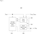
- FIG. 2 is a diagram illustrating an embodiment of a band gap reference circuit 200 under a low supply voltage according to the present disclosure.
- the band gap reference circuit 200 under a low supply voltage includes a band gap reference main circuit unit Voltage Reference Main Circuit 210 and a transimpedance amplifier 250.
- the Voltage Reference Main Circuit 210 generates a first node voltage V N1 and a second node voltage V N2 in response to a first bias voltage V BIAS1 and a band gap reference voltage V REF .
- the transimpedance amplifier 250 includes a bias stage Bias Stage 220 and an inter amplifying stage Inter Amplifying Stage 230 that generate the band gap reference voltage V REF by amplifying the first node voltage V N1 and the second node voltage V N2 using the first bias voltage V BIAS1 , a second bias voltage V BIAS2 , and a third bias voltage V BIAS3 .
- the first bias voltage V BIAS1 to the third bias voltage V BIAS3 are voltages generated externally and applied to the band gap reference circuit 200 under a low supply voltage according to the present disclosure.
- the voltage levels of the first bias voltage V BIAS1 to the third bias voltage V BIAS3 can be set to 0.86 V (Volts), 0.52 V, and 1.34 V, respectively.
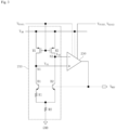
- FIG. 3 is a diagram illustrating an embodiment of an internal configuration of the band gap reference circuit under a low supply voltage according to the present disclosure.
- the Voltage Reference Main Circuit 210 includes a first MOS transistor M1, a second MOS transistor M2, a first bipolar transistor B1, a second bipolar transistor B2, a first resistor R1, and a second resistor R2, and the transimpedance amplifier 250 is expressed in the form of a differential amplifier.
- the first MOS transistor M1 has one terminal connected to the power supply voltage V DD , another terminal connected to a first node N1, and a gate terminal to which the first bias voltage V BIAS1 is applied.
- the second MOS transistor M2 has one terminal connected to the power supply voltage V DD , another terminal connected to a second node N2, and a gate terminal to which the first bias voltage V BIAS1 is applied.
- the voltage level of the first node N1 is defined as V N1 and the voltage level of the second node N2 is defined as V N2 .
- the first bipolar transistor B1 has one terminal connected to the first node N1, and a base terminal to which the band gap reference voltage V REF is applied.
- the second bipolar transistor B2 has one terminal connected to the second node N2, and a base terminal to which the band gap reference voltage V REF is applied.
- the first resistor R1 has one terminal connected to another terminal of the first bipolar transistor B1.
- the second resistor R2 has one terminal commonly connected to the other terminal of the first resistor R1 and another terminal of the second bipolar transistor B2, and the other terminal connected to a ground voltage GND.
- the transimpedance amplifier 250 generates the band gap reference voltage V REF by amplifying the first node voltage V N1 and the second node voltage V N2 using the first bias voltage V BIAS1 , the second bias voltage V BIAS2 , and the third bias voltage V BIAS3 .
- the present disclosure proposes the use of the transimpedance amplifier 250.
- the transimpedance amplifier 250 generates the band gap reference voltage V REF by amplifying the difference between the two input voltages V N1 and V N2 , and the band gap reference voltage V REF controls currents flowing through the two bipolar transistors B1 and B2, so that the two node voltages V N1 and V N2 are made equal to each other as a result.
- the transimpedance amplifier 250 includes the Bias Stage 220 and the Inter Amplifying Stage 230, and actual configurations of the Bias Stage 220 and the Inter Amplifying Stage 230 will be described below.
- the Bias Stage 220 and the Inter Amplifying Stage 230 according to embodiments will be distinguished using reference sign '-'.
- reference signs of the bias stage 220 according to two embodiments are 220-1 and 220-2, respectively.
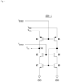
- FIG. 4 is a diagram illustrating an embodiment of the bias stage constituting the transimpedance amplifier.
- the bias stage 220-1 generates a fourth node voltage V N4 by using the second bias voltage V BIAS2 , the third bias voltage V BIAS3 , the first node voltage V N1 , and the second node voltage V N2 , and includes a third MOS transistor M3, a fourth MOS transistor M4, a fifth MOS transistor M5, a sixth MOS transistor M6, a seventh MOS transistor M7, and an eighth MOS transistor M8.
- the third MOS transistor M3 has one terminal connected to the first node N1, another terminal connected to a fourth node N4, and a gate terminal to which the second bias voltage V BIAS2 is applied.
- the fourth MOS transistor M4 has one terminal connected to the second node N2 and a gate terminal to which the second bias voltage V BIAS2 is applied.
- the fifth MOS transistor M5 has one terminal connected to the fourth node N4, and a gate terminal to which the third bias voltage V BIAS3 is applied.
- the sixth MOS transistor M6 has one terminal connected to another terminal of the fourth MOS transistor M4, and a gate terminal to which the third bias voltage V BIAS3 is applied.
- the seventh MOS transistor M7 has one terminal connected to another terminal of the fifth MOS transistor M5, another terminal connected to the ground voltage GND, and a gate terminal connected to a common terminal between the fourth MOS transistor M4 and the sixth MOS transistor M6.
- the eighth MOS transistor M8 has one terminal connected to another terminal of the sixth MOS transistor M6, another terminal connected to the ground voltage GND, and a gate terminal connected to the gate terminal of the seventh MOS transistor M7.
- a voltage level of the fourth node N4 is indicated by V N4
- the fourth node and the voltage level of the fourth node are the same as the explanation logic for the first node N1 and the second node N2, and the same applies in the following description.
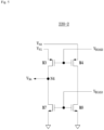
- FIG. 5 is a diagram illustrating another embodiment of the bias stage constituting the transimpedance amplifier.
- the bias stage 220-2 generates the fourth node voltage V N4 by using the second bias voltage V BIAS2 and the third bias voltage V BIAS3 , and includes the third MOS transistor M3, the fourth MOS transistor M4, the seventh MOS transistor M7, and the eighth MOS transistor M8.
- the third MOS transistor M3 has one terminal connected to the first node N1, another terminal connected to the fourth node N4, and a gate terminal to which the second bias voltage V BIAS2 is applied.
- the fourth MOS transistor M4 has one terminal connected to the second node N2 and a gate terminal to which the second bias voltage V BIAS2 is applied.
- the seventh MOS transistor M7 has one terminal connected to the fourth node N4, another terminal connected to the ground voltage GND, and a gate terminal to which the third bias voltage V BIAS3 is applied.
- the eighth MOS transistor M8 has one terminal connected to another terminal of the fourth MOS transistor M4, another terminal connected to the ground voltage GND, and a gate terminal to which the third bias voltage V BIAS3 is applied.
- the third MOS transistor M3 and the fourth MOS transistor M4 are P-type MOS transistors
- the fifth MOS transistor M5 to the eighth MOS transistor M8 are N-type MOS transistors, and the same applies in the following description.
- the fourth node N4 generates the fourth node voltage V N4 in the same manner.
- FIG. 6 is a diagram illustrating a specific embodiment of the inter amplifying stage.
- the Inter Amplifying Stage 230-1 generates the band gap reference voltage V REF by amplifying the applied fourth node voltage V N4 , and to this end, includes two amplifiers INV1 and INV2 serially connected to each other.
- the first amplifier INV1 includes a ninth MOS transistor M9 having one terminal connected to the power supply voltage V DD and a gate terminal to which the first bias voltage V BIAS1 is applied, and a tenth MOS transistor M10 having one terminal connected to another terminal of the ninth MOS transistor M9, another terminal connected to the ground voltage GND, and a gate terminal to which the fourth node voltage V N4 is applied.
- the second amplifier INV2 includes an eleventh MOS transistor M11 having one terminal connected to the power supply voltage V DD , a gate terminal to which the first bias voltage V BIAS1 is applied, and a twelfth MOS transistor M12 having one terminal connected to another terminal of the eleventh MOS transistor M11, another terminal connected to the ground voltage GND, and a gate terminal connected to a common terminal between the ninth MOS transistor M9 being an output terminal of the first amplifier INV1 and the tenth MOS transistor M10.
- the band gap reference voltage V REF is output to a common terminal between the eleventh MOS transistor M11 and the twelfth MOS transistor M12.
- FIG. 7 is a diagram illustrating a specific embodiment of the inter amplifying stage.
- the Inter Amplifying Stage 230-2 generates the band gap reference voltage V REF by amplifying the applied fourth node voltage V N4 , and to this end, includes one amplifier INV1.
- the first amplifier INV1 includes a ninth MOS transistor M9 having one terminal connected to the power supply voltage V DD , another terminal that generates the band gap reference voltage V REF , and a gate terminal to which the first bias voltage V BIAS1 is applied, and a tenth MOS transistor M10 having one terminal that generates the band gap reference voltage V REF , another terminal connected to the ground voltage GND, and a gate terminal to which the fourth node voltage V N4 is applied.
- the two amplifiers INV1 and INV2 included in the Inter Amplifying Stage 230 have the same structure as an inverter, and one of the electrical characteristics of the inverter may be the amplification of an input signal.
- the ninth MOS transistor M9 and the eleventh MOS transistor M11 serve as loads, respectively.
- FIG. 8 is a diagram illustrating a specific embodiment of the band gap reference circuit under a low supply voltage according to the present disclosure.
- FIG. 9 is a diagram illustrating another specific embodiment of the band gap reference circuit under a low supply voltage according to the present disclosure.
- the band gap reference circuit 200 under a low supply voltage includes a main circuit unit 210 and a transimpedance amplifier 250, and the transimpedance amplifier 250 includes the bias stage 220-1 illustrated in FIG. 4 and the Inter Amplifying Stage 230-1 illustrated in FIG. 6 .
- the band gap reference circuit 200 under a low supply voltage includes a main circuit unit 210 and a transimpedance amplifier 250, and the transimpedance amplifier 250 includes the bias stage 220-2 illustrated in FIG. 5 and the Inter Amplifying Stage 230-1 illustrated in FIG. 6 .
Landscapes
- Engineering & Computer Science (AREA)
- Physics & Mathematics (AREA)
- Microelectronics & Electronic Packaging (AREA)
- Electromagnetism (AREA)
- General Physics & Mathematics (AREA)
- Radar, Positioning & Navigation (AREA)
- Automation & Control Theory (AREA)
- Power Engineering (AREA)
- Nonlinear Science (AREA)
- Control Of Electrical Variables (AREA)
- Amplifiers (AREA)
Abstract
Description
- The present disclosure relates to a band gap reference circuit, and more particularly, to a band gap reference circuit under a low supply voltage capable of generating a band gap reference voltage in a semiconductor device having a low level of an operating voltage.
- Semiconductor devices include various circuits for generating, processing, and storing data. Such semiconductor devices receive voltages having various voltage levels from an external power source or operate using a voltage (hereinafter, referred to as a reference voltage) generated inside a circuit. Since a reference voltage generation circuit that generates a voltage having a specific voltage level includes an element with electrical characteristics varying depending on the temperature of a semiconductor device, the level of a reference voltage generated varies depending on the temperature of a corresponding semiconductor device even in a reference voltage generation circuit implemented in the same semiconductor.
- Circuits implemented in a semiconductor device operate according to a reference voltage supplied, and when the voltage level of a band gap reference voltage varies, output values of the circuits also vary, which is not what a circuit designer wants.
- In order to prevent abnormal operations of the circuits implemented in the semiconductor device or operations in a manner not desired by the designer and to ensure the circuit reliability, a band gap reference circuit that generates a band gap reference voltage is used.
- The band gap reference circuit is a circuit that generates a band gap reference voltage insensitive to changes in the temperature of the semiconductor device by using a band gap of silicon being a material of the semiconductor device. The band gap refers to an energy region where a charge state density between a valence band and a conduction band is zero in a semiconductor and an insulator and the energy difference, and the electrical conductivity of a material is determined by the size of the band gap.
-
FIG. 1 is a diagram illustrating an example of a bandgap reference circuit 100 in the related art. - Referring to
FIG. 1 , the bandgap reference circuit 100 in the related art generates a band gap reference voltage VREF insensitive to temperature changes by using two bipolar transistors Q1 and Q2 having different areas so that a component proportional to changes in absolute temperature (proportional to absolute temperature (PTAT)) and a component inversely proportional to changes in absolute temperature (complementary to absolute temperature (CTAT)) are offset to each other. - Since the electrical operating characteristics of the band
gap reference circuit 100 illustrated inFIG. 1 are known to those skilled in the art, description thereof will be omitted. - The voltage level of a reference voltage used in the circuit is closely related to the power consumption of the circuit. For example, it can be easily expected that the power consumption of a circuit operating between 5 V (volts) and a ground voltage GND is greater than the power consumption of a circuit operating between 3 V and a ground voltage. Recently, in order to minimize the power consumption of a semiconductor device, the voltage level of a supply voltage of the semiconductor device tends to be reduced.
- Referring to
FIG. 1 , it is disadvantageous that a metal oxide silicon transistor M4, in which a source terminal is connected to a power supply voltage VDD and gate and drain terminals are diode connected to be connected to the bipolar transistor Q2, may limit the operating voltage range of the bipolar transistor Q2 by a difference voltage VDD-VD between the power supply voltage VDD and a voltage VD of the drain terminal. - When the voltage level of a power supply voltage of a semiconductor device is reduced, the operation of a band gap reference circuit may not be possible.
- One object of the present disclosure is directed to providing a band gap reference circuit under a low supply voltage capable of generating a band gap reference voltage even under a low supply voltage by using a plurality of bias voltages separately generated and a current source using these bias voltages without using a diode connected structure used in the related art while not being affected by limitations in the operating voltage of a bipolar transistor.
- One or more of these objects is solved by the features of the independent claim. Technical problems to be achieved in the present disclosure are not limited to the aforementioned technical problems and the other unmentioned technical problems will be clearly understood by those skilled in the art from the following description.
- A band gap reference circuit, e.g. a band gap reference circuit under a low supply voltage, according to an aspect of the present disclosure includes: a voltage reference main circuit configured to generate a first node voltage and a second node voltage in response to a first bias voltage and a band gap reference voltage; and a transimpedance amplifier configured to generate the band gap reference voltage by amplifying a difference between the first node voltage and the second node voltage using the first bias voltage, a second bias voltage, and a third bias voltage.
- A band gap reference circuit, e.g. a band gap reference circuit under a low supply voltage, according to another aspect of the present disclosure includes: a voltage reference main circuit configured to generate a first node voltage and a second node voltage in response to a first bias voltage and a band gap reference voltage; a bias stage configured to generate a fourth node voltage by using a second bias voltage, a third bias voltage, the first node voltage, and the second node voltage; and an inter amplifying stage configured to generate the band gap reference voltage by amplifying the fourth node voltage using the first bias voltage.
- The band gap reference circuit according to any one of these aspects may include one or more of the following preferred features:
- The voltage reference main circuit may comprise a first MOS transistor including one terminal connected to a power supply voltage, another terminal connected to a first node that generates the first node voltage, and a gate terminal to which the first bias voltage is applied. The voltage reference main circuit may comprise a second MOS transistor including one terminal connected to the power supply voltage, another terminal connected to a second node that generates the second node voltage, and a gate terminal to which the first bias voltage is applied. The voltage reference main circuit may comprise a first bipolar transistor including one terminal connected to the first node and a base terminal to which the band gap reference voltage is applied. The voltage reference main circuit may comprise a second bipolar transistor including one terminal connected to the second node, another terminal connected to a ground voltage, and a base terminal to which the band gap reference voltage is applied. The voltage reference main circuit may comprise a first resistor including one terminal connected to another terminal of the first bipolar transistor and the other terminal connected to the ground voltage; and/or a second resistor including one terminal commonly connected to the other terminal of the first resistor and another terminal of the second bipolar transistor, and the other terminal connected to the ground voltage.
- The transimpedance amplifier may comprise a bias stage configured to generate a fourth node voltage by using the second bias voltage, the third bias voltage, the first node voltage, and the second node voltage. The transimpedance amplifier may comprise further an inter amplifying stage configured to generate the band gap reference voltage by amplifying the fourth node voltage using the first bias voltage.
- The bias stage may comprise a third MOS transistor including one terminal connected to a first node that generates the first node voltage, another terminal connected to a fourth node that generates the fourth node voltage, and a gate terminal to which the second bias voltage is applied. The bias stage may comprise a fourth MOS transistor including one terminal connected to a second node that generates the second node voltage and a gate terminal to which the second bias voltage is applied. The bias stage may comprise a fifth MOS transistor including one terminal connected to the fourth node and a gate terminal to which the third bias voltage is applied. The bias stage may comprise a sixth MOS transistor including one terminal connected to another terminal of the fourth MOS transistor and a gate terminal to which the third bias voltage is applied. The bias stage may comprise a seventh MOS transistor including one terminal connected to another terminal of the fifth MOS transistor, another terminal connected to the ground voltage, and a gate terminal connected to a common terminal between the fourth MOS transistor and the sixth MOS transistor. The bias stage may comprise an eighth MOS transistor including one terminal connected to another terminal of the sixth MOS transistor, another terminal connected to the ground voltage, and a gate terminal connected to the gate terminal of the seventh MOS transistor.
- The bias stage may comprise a third MOS transistor including one terminal connected to a first node that generates the first node voltage, another terminal connected to a fourth node that generates the fourth node voltage, and a gate terminal to which the second bias voltage is applied. The bias stage may comprise a fourth MOS transistor including one terminal connected to a second node that generates the second node voltage and a gate terminal to which the second bias voltage is applied. The bias stage may comprise a seventh MOS transistor including one terminal connected to the fourth node, another terminal connected to the ground voltage, and a gate terminal to which the third bias voltage is applied. The bias stage may comprise an eighth MOS transistor including one terminal connected to another terminal of the fourth MOS transistor, another terminal connected to the ground voltage, and a gate terminal to which the third bias voltage is applied.
- The inter amplifying stage may comprise a first amplifier configured to amplify the fourth node voltage and/or a second amplifier configured to generate the band gap reference voltage by amplifying output of the first amplifier.
- The first amplifier may comprise a ninth MOS transistor including one terminal connected to a power supply voltage and a gate terminal to which the first bias voltage is applied. The first amplifier may comprise a tenth MOS transistor including one terminal connected to another terminal of the ninth MOS transistor, another terminal connected to the ground voltage, and a gate terminal to which the fourth node voltage is applied.
- The second amplifier may comprise an eleventh MOS transistor including one terminal connected to the power supply voltage, another terminal that generates the band gap reference voltage, and a gate terminal to which the first bias voltage is applied. The second amplifier may comprise a twelfth MOS transistor including one terminal that generates the band gap reference voltage, another terminal connected to the ground voltage, and a gate terminal connected to a common terminal between the ninth MOS transistor and the tenth MOS transistor.
- The inter amplifying stage may comprise a ninth MOS transistor including one terminal connected to the power supply voltage and another terminal that generates the band gap reference voltage. The inter amplifying stage may comprise a tenth MOS transistor including one terminal that generates the band gap reference voltage, another terminal connected to the ground voltage, and a gate terminal to which the fourth node voltage is applied.
- Technical problems to be achieved in the present disclosure are not limited to the aforementioned technical problems and the other unmentioned technical problems will be clearly understood by those skilled in the art from the following description.
- A band gap reference circuit under a low supply voltage according to the present disclosure as described above has the advantage capable of generating a band gap reference voltage even under a low supply voltage by using a plurality of bias voltages separately generated and a current source using these bias voltages without using a diode connected structure used in the related art while not being affected by limitations in the operating voltage of a bipolar transistor.
- Effects achievable in the disclosure are not limited to the aforementioned effects and the other unmentioned effects will be clearly understood by those skilled in the art from the following description.
-
-
FIG. 1 is a diagram illustrating an example of a band gap reference circuit in the related art. -
FIG. 2 is a diagram illustrating an embodiment of a band gap reference circuit under a low supply voltage according to the present disclosure. -
FIG. 3 is a diagram illustrating an embodiment of an internal configuration of a band gap reference circuit under a low supply voltage according to the present disclosure. -
FIG. 4 is a diagram illustrating an embodiment of a bias stage constituting a transimpedance amplifier. -
FIG. 5 is a diagram illustrating another embodiment of a bias stage constituting a transimpedance amplifier. -
FIG. 6 is a diagram illustrating a specific embodiment of an inter amplifying stage. -
FIG. 7 is a diagram illustrating a specific embodiment of an inter amplifying stage. -
FIG. 8 is a diagram illustrating a specific embodiment of a band gap reference circuit under a low supply voltage according to the present disclosure. -
FIG. 9 is a diagram illustrating another specific embodiment of a band gap reference circuit under a low supply voltage according to the present disclosure. - In order to fully understand the present disclosure, advantages in operation of the present disclosure, and objects achieved by carrying out the present disclosure, the accompanying drawings for explaining exemplary examples of the present disclosure and the contents described with reference to the accompanying drawings need to be referred to.
- Hereinafter, preferred embodiments of the present disclosure are described in detail with reference to the accompanying drawings. The same reference numerals among the reference numerals in each drawing indicate the same members.
-
FIG. 2 is a diagram illustrating an embodiment of a bandgap reference circuit 200 under a low supply voltage according to the present disclosure. - Referring to
FIG. 2 , the bandgap reference circuit 200 under a low supply voltage according to the present disclosure includes a band gap reference main circuit unit VoltageReference Main Circuit 210 and atransimpedance amplifier 250. - The Voltage
Reference Main Circuit 210 generates a first node voltage VN1 and a second node voltage VN2 in response to a first bias voltage VBIAS1 and a band gap reference voltage VREF. - The
transimpedance amplifier 250 includes a biasstage Bias Stage 220 and an inter amplifying stageInter Amplifying Stage 230 that generate the band gap reference voltage VREF by amplifying the first node voltage VN1 and the second node voltage VN2 using the first bias voltage VBIAS1, a second bias voltage VBIAS2, and a third bias voltage VBIAS3. - The first bias voltage VBIAS1 to the third bias voltage VBIAS3 are voltages generated externally and applied to the band
gap reference circuit 200 under a low supply voltage according to the present disclosure. - For example, assuming that the voltage level of a power supply voltage VDD is 1.8 V (Volts), the voltage levels of the first bias voltage VBIAS1 to the third bias voltage VBIAS3 can be set to 0.86 V (Volts), 0.52 V, and 1.34 V, respectively.
-
FIG. 3 is a diagram illustrating an embodiment of an internal configuration of the band gap reference circuit under a low supply voltage according to the present disclosure. - Referring to
FIG. 3 , the VoltageReference Main Circuit 210 includes a first MOS transistor M1, a second MOS transistor M2, a first bipolar transistor B1, a second bipolar transistor B2, a first resistor R1, and a second resistor R2, and thetransimpedance amplifier 250 is expressed in the form of a differential amplifier. - The first MOS transistor M1 has one terminal connected to the power supply voltage VDD, another terminal connected to a first node N1, and a gate terminal to which the first bias voltage VBIAS1 is applied. The second MOS transistor M2 has one terminal connected to the power supply voltage VDD, another terminal connected to a second node N2, and a gate terminal to which the first bias voltage VBIAS1 is applied. In
FIG. 3 , the voltage level of the first node N1 is defined as VN1 and the voltage level of the second node N2 is defined as VN2. - The first bipolar transistor B1 has one terminal connected to the first node N1, and a base terminal to which the band gap reference voltage VREF is applied. The second bipolar transistor B2 has one terminal connected to the second node N2, and a base terminal to which the band gap reference voltage VREF is applied.
- The first resistor R1 has one terminal connected to another terminal of the first bipolar transistor B1. The second resistor R2 has one terminal commonly connected to the other terminal of the first resistor R1 and another terminal of the second bipolar transistor B2, and the other terminal connected to a ground voltage GND.
- Referring to
FIG. 3 , it can be seen that thetransimpedance amplifier 250 generates the band gap reference voltage VREF by amplifying the first node voltage VN1 and the second node voltage VN2 using the first bias voltage VBIAS1, the second bias voltage VBIAS2, and the third bias voltage VBIAS3. - Referring to
FIG. 3 , in order to generate the band gap reference voltage VREF insensitive to temperature changes from the twobipolar transistors B 1 and B2, currents flowing through the two MOS transistors M1 and M2 need to be equal to each other by making the voltage levels of the two node voltages VN1 and VN2 equal to each other, and to this end, the present disclosure proposes the use of thetransimpedance amplifier 250. - That is, the
transimpedance amplifier 250 generates the band gap reference voltage VREF by amplifying the difference between the two input voltages VN1 and VN2, and the band gap reference voltage VREF controls currents flowing through the two bipolar transistors B1 and B2, so that the two node voltages VN1 and VN2 are made equal to each other as a result. - Referring to
FIG. 2 , thetransimpedance amplifier 250 includes theBias Stage 220 and theInter Amplifying Stage 230, and actual configurations of theBias Stage 220 and theInter Amplifying Stage 230 will be described below. In the following description, theBias Stage 220 and theInter Amplifying Stage 230 according to embodiments will be distinguished using reference sign '-'. For example, reference signs of thebias stage 220 according to two embodiments are 220-1 and 220-2, respectively. -
FIG. 4 is a diagram illustrating an embodiment of the bias stage constituting the transimpedance amplifier. - Referring to
FIG. 4 , the bias stage 220-1 generates a fourth node voltage VN4 by using the second bias voltage VBIAS2, the third bias voltage VBIAS3, the first node voltage VN1, and the second node voltage VN2, and includes a third MOS transistor M3, a fourth MOS transistor M4, a fifth MOS transistor M5, a sixth MOS transistor M6, a seventh MOS transistor M7, and an eighth MOS transistor M8. - The third MOS transistor M3 has one terminal connected to the first node N1, another terminal connected to a fourth node N4, and a gate terminal to which the second bias voltage VBIAS2 is applied.
- The fourth MOS transistor M4 has one terminal connected to the second node N2 and a gate terminal to which the second bias voltage VBIAS2 is applied.
- The fifth MOS transistor M5 has one terminal connected to the fourth node N4, and a gate terminal to which the third bias voltage VBIAS3 is applied.
- The sixth MOS transistor M6 has one terminal connected to another terminal of the fourth MOS transistor M4, and a gate terminal to which the third bias voltage VBIAS3 is applied.
- The seventh MOS transistor M7 has one terminal connected to another terminal of the fifth MOS transistor M5, another terminal connected to the ground voltage GND, and a gate terminal connected to a common terminal between the fourth MOS transistor M4 and the sixth MOS transistor M6.
- The eighth MOS transistor M8 has one terminal connected to another terminal of the sixth MOS transistor M6, another terminal connected to the ground voltage GND, and a gate terminal connected to the gate terminal of the seventh MOS transistor M7.
- In the above description, a voltage level of the fourth node N4 is indicated by VN4, the fourth node and the voltage level of the fourth node are the same as the explanation logic for the first node N1 and the second node N2, and the same applies in the following description.
-
FIG. 5 is a diagram illustrating another embodiment of the bias stage constituting the transimpedance amplifier. - Referring to
FIG. 5 , the bias stage 220-2 generates the fourth node voltage VN4 by using the second bias voltage VBIAS2 and the third bias voltage VBIAS3, and includes the third MOS transistor M3, the fourth MOS transistor M4, the seventh MOS transistor M7, and the eighth MOS transistor M8. - The third MOS transistor M3 has one terminal connected to the first node N1, another terminal connected to the fourth node N4, and a gate terminal to which the second bias voltage VBIAS2 is applied.
- The fourth MOS transistor M4 has one terminal connected to the second node N2 and a gate terminal to which the second bias voltage VBIAS2 is applied.
- The seventh MOS transistor M7 has one terminal connected to the fourth node N4, another terminal connected to the ground voltage GND, and a gate terminal to which the third bias voltage VBIAS3 is applied.
- The eighth MOS transistor M8 has one terminal connected to another terminal of the fourth MOS transistor M4, another terminal connected to the ground voltage GND, and a gate terminal to which the third bias voltage VBIAS3 is applied.
- The third MOS transistor M3 and the fourth MOS transistor M4 are P-type MOS transistors, the fifth MOS transistor M5 to the eighth MOS transistor M8 are N-type MOS transistors, and the same applies in the following description.
- In
FIGS. 4 and5 , the fourth node N4 generates the fourth node voltage VN4 in the same manner. -
FIG. 6 is a diagram illustrating a specific embodiment of the inter amplifying stage. - Referring to
FIG. 6 , the Inter Amplifying Stage 230-1 generates the band gap reference voltage VREF by amplifying the applied fourth node voltage VN4, and to this end, includes two amplifiers INV1 and INV2 serially connected to each other. - The first amplifier INV1 includes a ninth MOS transistor M9 having one terminal connected to the power supply voltage VDD and a gate terminal to which the first bias voltage VBIAS1 is applied, and a tenth MOS transistor M10 having one terminal connected to another terminal of the ninth MOS transistor M9, another terminal connected to the ground voltage GND, and a gate terminal to which the fourth node voltage VN4 is applied.
- The second amplifier INV2 includes an eleventh MOS transistor M11 having one terminal connected to the power supply voltage VDD, a gate terminal to which the first bias voltage VBIAS1 is applied, and a twelfth MOS transistor M12 having one terminal connected to another terminal of the eleventh MOS transistor M11, another terminal connected to the ground voltage GND, and a gate terminal connected to a common terminal between the ninth MOS transistor M9 being an output terminal of the first amplifier INV1 and the tenth MOS transistor M10.
- The band gap reference voltage VREF is output to a common terminal between the eleventh MOS transistor M11 and the twelfth MOS transistor M12.
-
FIG. 7 is a diagram illustrating a specific embodiment of the inter amplifying stage. - Referring to
FIG. 7 , the Inter Amplifying Stage 230-2 generates the band gap reference voltage VREF by amplifying the applied fourth node voltage VN4, and to this end, includes one amplifier INV1. - The first amplifier INV1 includes a ninth MOS transistor M9 having one terminal connected to the power supply voltage VDD, another terminal that generates the band gap reference voltage VREF, and a gate terminal to which the first bias voltage VBIAS1 is applied, and a tenth MOS transistor M10 having one terminal that generates the band gap reference voltage VREF, another terminal connected to the ground voltage GND, and a gate terminal to which the fourth node voltage VN4 is applied.
- The two amplifiers INV1 and INV2 included in the
Inter Amplifying Stage 230 have the same structure as an inverter, and one of the electrical characteristics of the inverter may be the amplification of an input signal. - In the structures of the inverters illustrated in
FIGS. 6 and7 , the ninth MOS transistor M9 and the eleventh MOS transistor M11 serve as loads, respectively. -
FIG. 8 is a diagram illustrating a specific embodiment of the band gap reference circuit under a low supply voltage according to the present disclosure. -
FIG. 9 is a diagram illustrating another specific embodiment of the band gap reference circuit under a low supply voltage according to the present disclosure. - Referring to
FIG. 8 , the bandgap reference circuit 200 under a low supply voltage according to the present disclosure includes amain circuit unit 210 and atransimpedance amplifier 250, and thetransimpedance amplifier 250 includes the bias stage 220-1 illustrated inFIG. 4 and the Inter Amplifying Stage 230-1 illustrated inFIG. 6 . - Referring to
FIG. 9 , the bandgap reference circuit 200 under a low supply voltage according to the present disclosure includes amain circuit unit 210 and atransimpedance amplifier 250, and thetransimpedance amplifier 250 includes the bias stage 220-2 illustrated inFIG. 5 and the Inter Amplifying Stage 230-1 illustrated inFIG. 6 . - Although the technical spirit of the present disclosure has been described together with the accompanying drawings, this is an illustrative example of a preferred embodiment of the present disclosure, but does not limit the present disclosure. In addition, it is clear that various modifications and imitations can be made by anyone skilled in the art to which the present disclosure belongs without departing from the scope of the present disclosure.
Claims (15)
- A band gap reference circuit under a low supply voltage comprising:a voltage reference main circuit (210) configured to generate a first node voltage (VN1) and a second node voltage (VN2) in response to a first bias voltage (VBIAS1) and a band gap reference voltage (VREF); anda transimpedance amplifier (250) configured to generate the band gap reference voltage (VREF) by amplifying a difference between the first node voltage (VN1) and the second node voltage (VN2) using the first bias voltage (VBIAS1), a second bias voltage (VBIAS2), and a third bias voltage (VBIAS3).
- The band gap reference circuit under a low supply voltage of claim 1, wherein the voltage reference main circuit (210) comprises:a first MOS transistor (M1) including one terminal connected to a power supply voltage VDD, another terminal connected to a first node (N1) configured to generate the first node voltage, and a gate terminal to which the first bias voltage is applied;a second MOS transistor (M2) including one terminal connected to the power supply voltage, another terminal connected to a second node configured to generate the second node voltage, and a gate terminal to which the first bias voltage is applied;a first bipolar transistor (B 1) including one terminal connected to the first node and a base terminal to which the band gap reference voltage is applied;a second bipolar transistor (B2) including one terminal connected to the second node, another terminal connected to a ground voltage, and a base terminal to which the band gap reference voltage is applied;a first resistor (R1) including one terminal connected to another terminal of the first bipolar transistor and the other terminal connected to the ground voltage; anda second resistor (R2) including one terminal commonly connected to the other terminal of the first resistor and another terminal of the second bipolar transistor, and the other terminal connected to the ground voltage.
- The band gap reference circuit under a low supply voltage of claim 1 or 2, wherein the transimpedance amplifier (250) comprises:a bias stage (220) configured to generate a fourth node voltage by using the second bias voltage, the third bias voltage, the first node voltage, and the second node voltage; andan inter amplifying stage (230) configured to generate the band gap reference voltage by amplifying the fourth node voltage using the first bias voltage.
- The band gap reference circuit under a low supply voltage of claim 3, wherein the bias stage (220-1) comprises:a third MOS transistor (M3) including one terminal connected to a first node that generates the first node voltage, another terminal connected to a fourth node that generates the fourth node voltage, and a gate terminal to which the second bias voltage is applied;a fourth MOS transistor (M4) including one terminal connected to a second node that generates the second node voltage and a gate terminal to which the second bias voltage is applied;a fifth MOS transistor (M5) including one terminal connected to the fourth node and a gate terminal to which the third bias voltage is applied;a sixth MOS transistor (M6) including one terminal connected to another terminal of the fourth MOS transistor and a gate terminal to which the third bias voltage is applied;a seventh MOS transistor (M7) including one terminal connected to another terminal of the fifth MOS transistor, another terminal connected to the ground voltage, and a gate terminal connected to a common terminal between the fourth MOS transistor and the sixth MOS transistor; andan eighth MOS transistor (M8) including one terminal connected to another terminal of the sixth MOS transistor, another terminal connected to the ground voltage, and a gate terminal connected to the gate terminal of the seventh MOS transistor.
- The band gap reference circuit under a low supply voltage of claim 3, wherein the bias stage (220-2) comprises:a third MOS transistor (M3) including one terminal connected to a first node that generates the first node voltage, another terminal connected to a fourth node configured to generate the fourth node voltage, and a gate terminal to which the second bias voltage is applied;a fourth MOS transistor (M4) including one terminal connected to a second node that generates the second node voltage and a gate terminal to which the second bias voltage is applied;a seventh MOS transistor (M7) including one terminal connected to the fourth node, another terminal connected to the ground voltage, and a gate terminal to which the third bias voltage is applied; andan eighth MOS transistor (M8) including one terminal connected to another terminal of the fourth MOS transistor, another terminal connected to the ground voltage, and a gate terminal to which the third bias voltage is applied.
- The band gap reference circuit under a low supply voltage of claim 3, 4 or 5, wherein the inter amplifying stage (230-1) comprises:a first amplifier (INV1) configured to amplify the fourth node voltage; anda second amplifier (INV2) configured to generate the band gap reference voltage by amplifying output of the first amplifier.
- The band gap reference circuit under a low supply voltage of claim 6, wherein the first amplifier comprises:a ninth MOS transistor (M9) including one terminal connected to a power supply voltage and a gate terminal to which the first bias voltage is applied; anda tenth MOS transistor (M10) including one terminal connected to another terminal of the ninth MOS transistor, another terminal connected to the ground voltage, and a gate terminal to which the fourth node voltage is applied; and/orwherein the second amplifier comprises:an eleventh MOS transistor (M11) including one terminal connected to the power supply voltage, another terminal that generates the band gap reference voltage, and a gate terminal to which the first bias voltage is applied; anda twelfth MOS transistor (M12) including one terminal that generates the band gap reference voltage, another terminal connected to the ground voltage, and a gate terminal connected to a common terminal between the ninth MOS transistor and the tenth MOS transistor.
- The band gap reference circuit under a low supply voltage of claim 3, 4 or 5, wherein the inter amplifying stage (230-2) comprises:a ninth MOS transistor (M9) including one terminal connected to the power supply voltage and another terminal that generates the band gap reference voltage; anda tenth MOS transistor (M10) including one terminal that generates the band gap reference voltage, another terminal connected to the ground voltage, and a gate terminal to which the fourth node voltage is applied.
- A band gap reference circuit under a low supply voltage comprising:a voltage reference main circuit (210) configured to generate a first node voltage and a second node voltage in response to a first bias voltage and a band gap reference voltage;a bias stage (220) configured to generate a fourth node voltage by using a second bias voltage, a third bias voltage, the first node voltage, and the second node voltage; andan inter amplifying stage (230) configured to generate the band gap reference voltage by amplifying the fourth node voltage using the first bias voltage.
- The band gap reference circuit under a low supply voltage of claim 9, wherein the voltage reference main circuit (210) comprises:a first MOS transistor (M1) including one terminal connected to a power supply voltage, another terminal connected to a first node that generates the first node voltage, and a gate terminal to which the first bias voltage is applied;a second MOS transistor (M2) including one terminal connected to the power supply voltage, another terminal connected to a second node that generates the second node voltage, and a gate terminal to which the first bias voltage is applied;a first bipolar transistor (B 1) including one terminal connected to the first node and a base terminal to which the band gap reference voltage is applied;a second bipolar transistor (B2) including one terminal connected to the second node, another terminal connected to a ground voltage, and a base terminal to which the band gap reference voltage is applied;a first resistor (R1) including one terminal connected to another terminal of the first bipolar transistor and the other terminal connected to the ground voltage; anda second resistor (R2) including one terminal commonly connected to the other terminal of the first resistor and another terminal of the second bipolar transistor, and the other terminal connected to the ground voltage.
- The band gap reference circuit under a low supply voltage of claim 9, wherein the bias stage (220) comprises:a third MOS transistor (M3) including one terminal connected to a first node that generates the first node voltage, another terminal connected to a fourth node that generates the fourth node voltage, and a gate terminal to which the second bias voltage is applied;a fourth MOS transistor (M4) including one terminal connected to a second node that generates the second node voltage and a gate terminal to which the second bias voltage is applied;a fifth MOS transistor (M5) including one terminal connected to the fourth node and a gate terminal to which the third bias voltage is applied;a sixth MOS transistor (M6) including one terminal connected to another terminal of the fourth MOS transistor and a gate terminal to which the third bias voltage is applied;a seventh MOS transistor (M7) including one terminal connected to another terminal of the fifth MOS transistor, another terminal connected to the ground voltage, and a gate terminal connected to a common terminal between the fourth MOS transistor and the sixth MOS transistor; andan eighth MOS transistor (M8) including one terminal connected to another terminal of the sixth MOS transistor, another terminal connected to the ground voltage, and a gate terminal connected to the gate terminal of the seventh MOS transistor.
- The band gap reference circuit under a low supply voltage of claim 9, wherein the bias stage (220) comprises:a third MOS transistor (M3) including one terminal connected to a first node that generates the first node voltage, another terminal connected to a fourth node that generates the fourth node voltage, and a gate terminal to which the second bias voltage is applied;a fourth MOS transistor (M4) including one terminal connected to a second node that generates the second node voltage and a gate terminal to which the second bias voltage is applied;a seventh MOS transistor (M7) including one terminal connected to the fourth node, another terminal connected to the ground voltage, and a gate terminal to which the third bias voltage is applied; andan eighth MOS transistor (M8) including one terminal connected to another terminal of the fourth MOS transistor, another terminal connected to the ground voltage, and a gate terminal to which the third bias voltage is applied.
- The band gap reference circuit under a low supply voltage of claim 9, wherein the inter amplifying stage (230-1) comprises:a first amplifier configured to amplify the fourth node voltage; anda second amplifier configured to generate the band gap reference voltage by amplifying output of the first amplifier.
- The band gap reference circuit under a low supply voltage of claim 13, wherein the first amplifier comprises:a ninth MOS transistor including one terminal connected to the power supply voltage and a gate terminal to which the first bias voltage is applied; anda tenth MOS transistor including one terminal connected to another terminal of the ninth MOS transistor, another terminal connected to the ground voltage, and a gate terminal to which the fourth node voltage is applied,and wherein the second amplifier comprises:an eleventh MOS transistor including one terminal connected to the power supply voltage, another terminal that generates the band gap reference voltage, and a gate terminal to which the first bias voltage is applied; anda twelfth MOS transistor including one terminal that generates the band gap reference voltage, another terminal connected to the ground voltage, and a gate terminal connected to a common terminal between the ninth MOS transistor and the tenth MOS transistor.
- The band gap reference circuit under a low supply voltage of claim 9, wherein the inter amplifying stage (230-2) comprises:a ninth MOS transistor including one terminal connected to the power supply voltage and another terminal that generates the band gap reference voltage; anda tenth MOS transistor including one terminal that generates the band gap reference voltage, another terminal connected to the ground voltage, and a gate terminal to which the fourth node voltage is applied.
Applications Claiming Priority (2)
| Application Number | Priority Date | Filing Date | Title |
|---|---|---|---|
| KR20220160489 | 2022-11-25 | ||
| KR1020230081592A KR20240078299A (en) | 2022-11-25 | 2023-06-26 | Band gap reference circuit under low supply voltage |
Publications (2)
| Publication Number | Publication Date |
|---|---|
| EP4375788A2 true EP4375788A2 (en) | 2024-05-29 |
| EP4375788A3 EP4375788A3 (en) | 2025-01-01 |
Family
ID=88975925
Family Applications (1)
| Application Number | Title | Priority Date | Filing Date |
|---|---|---|---|
| EP23212179.8A Pending EP4375788A3 (en) | 2022-11-25 | 2023-11-27 | Band gap reference circuit under low supply voltage |
Country Status (3)
| Country | Link |
|---|---|
| US (1) | US12399522B2 (en) |
| EP (1) | EP4375788A3 (en) |
| TW (1) | TW202422265A (en) |
Family Cites Families (11)
| Publication number | Priority date | Publication date | Assignee | Title |
|---|---|---|---|---|
| US4242693A (en) | 1978-12-26 | 1980-12-30 | Fairchild Camera & Instrument Corporation | Compensation of VBE non-linearities over temperature by using high base sheet resistivity devices |
| US4795961A (en) * | 1987-06-10 | 1989-01-03 | Unitrode Corporation | Low-noise voltage reference |
| EP1229420B1 (en) * | 2001-01-31 | 2006-04-12 | STMicroelectronics S.r.l. | Bandgap type reference voltage source with low supply voltage |
| KR20060088163A (en) | 2005-02-01 | 2006-08-04 | 엘지전자 주식회사 | Reference voltage generator |
| US20070024325A1 (en) * | 2005-08-01 | 2007-02-01 | Chung-Kuang Chen | Sense amplifier with input offset compensation |
| KR101465598B1 (en) | 2008-06-05 | 2014-12-15 | 삼성전자주식회사 | Reference voltage generating apparatus and method |
| EP2905672A1 (en) | 2014-02-11 | 2015-08-12 | Dialog Semiconductor GmbH | An apparatus and method for a modified brokaw bandgap reference circuit for improved low voltage power supply |
| US9582021B1 (en) * | 2015-11-20 | 2017-02-28 | Texas Instruments Deutschland Gmbh | Bandgap reference circuit with curvature compensation |
| US20190109243A1 (en) * | 2017-10-06 | 2019-04-11 | Globalfoundries Inc. | Back-gate controlled varactor |
| US11402265B2 (en) | 2019-11-05 | 2022-08-02 | Texas Instruments Incorporated | Apparatus for integrated offset voltage for photodiode current amplifier |
| US11526191B2 (en) * | 2020-02-04 | 2022-12-13 | Texas Instruments Incorporated | Precision reference circuit |
-
2023
- 2023-11-24 TW TW112145707A patent/TW202422265A/en unknown
- 2023-11-24 US US18/518,770 patent/US12399522B2/en active Active
- 2023-11-27 EP EP23212179.8A patent/EP4375788A3/en active Pending
Also Published As
| Publication number | Publication date |
|---|---|
| TW202422265A (en) | 2024-06-01 |
| US20240176378A1 (en) | 2024-05-30 |
| US12399522B2 (en) | 2025-08-26 |
| EP4375788A3 (en) | 2025-01-01 |
Similar Documents
| Publication | Publication Date | Title |
|---|---|---|
| US6815941B2 (en) | Bandgap reference circuit | |
| CN100430857C (en) | CMOS Voltage Bandgap Reference with Improved Peak Headroom | |
| KR0139546B1 (en) | Operational amplifier circuit | |
| US8786324B1 (en) | Mixed voltage driving circuit | |
| CN110895423B (en) | System and method for proportional to absolute temperature circuit | |
| JPH0951266A (en) | Circuit and method for maintaining a substrate voltage at a desired value | |
| US6713993B2 (en) | High-voltage regulator including an external regulating device | |
| US12101068B2 (en) | Push-pull output driver and operational amplifier using same | |
| KR0126911B1 (en) | Circuit and method for voltage reference generating | |
| TWI632773B (en) | Low power consumption power-on reset circuit and reference signal circuit | |
| US20210286394A1 (en) | Current reference circuit with current mirror devices having dynamic body biasing | |
| CN111446949B (en) | Power-on reset circuit and integrated circuit | |
| JP2002124835A (en) | Operational amplifier circuit, constant voltage circuit and reference voltage circuit | |
| US20180287576A1 (en) | Transconductance amplifier | |
| US10712762B2 (en) | Semiconductor circuit and semiconductor system | |
| CN110568902B (en) | Reference voltage source circuit | |
| JP3195770B2 (en) | Reference voltage generation circuit | |
| US12399522B2 (en) | Band gap reference circuit under low supply voltage | |
| US4855624A (en) | Low-power bipolar-CMOS interface circuit | |
| US7868686B2 (en) | Band gap circuit | |
| US9300276B2 (en) | Oscillation control circuit for biasing ring oscillator by bandgap reference signal and related method | |
| JPH05250050A (en) | Reference voltage generating circuit | |
| US5225716A (en) | Semiconductor integrated circuit having means for suppressing a variation in a threshold level due to temperature variation | |
| US11482976B2 (en) | Differential amplifier | |
| US12130649B2 (en) | Bias current generation circuit and flash memory |
Legal Events
| Date | Code | Title | Description |
|---|---|---|---|
| PUAI | Public reference made under article 153(3) epc to a published international application that has entered the european phase |
Free format text: ORIGINAL CODE: 0009012 |
|
| STAA | Information on the status of an ep patent application or granted ep patent |
Free format text: STATUS: THE APPLICATION HAS BEEN PUBLISHED |
|
| AK | Designated contracting states |
Kind code of ref document: A2 Designated state(s): AL AT BE BG CH CY CZ DE DK EE ES FI FR GB GR HR HU IE IS IT LI LT LU LV MC ME MK MT NL NO PL PT RO RS SE SI SK SM TR |
|
| RIC1 | Information provided on ipc code assigned before grant |
Ipc: G05F 3/30 20060101AFI20240719BHEP |
|
| PUAL | Search report despatched |
Free format text: ORIGINAL CODE: 0009013 |
|
| AK | Designated contracting states |
Kind code of ref document: A3 Designated state(s): AL AT BE BG CH CY CZ DE DK EE ES FI FR GB GR HR HU IE IS IT LI LT LU LV MC ME MK MT NL NO PL PT RO RS SE SI SK SM TR |
|
| RIC1 | Information provided on ipc code assigned before grant |
Ipc: H03F 1/08 20060101ALI20241126BHEP Ipc: G05F 3/30 20060101AFI20241126BHEP |
|
| STAA | Information on the status of an ep patent application or granted ep patent |
Free format text: STATUS: REQUEST FOR EXAMINATION WAS MADE |
|
| 17P | Request for examination filed |
Effective date: 20250630 |