EP4375735A1 - Calibration method for phase modulator, calibration method for balanced photodetector, and calibration system for phase modulator - Google Patents
Calibration method for phase modulator, calibration method for balanced photodetector, and calibration system for phase modulator Download PDFInfo
- Publication number
- EP4375735A1 EP4375735A1 EP22845930.1A EP22845930A EP4375735A1 EP 4375735 A1 EP4375735 A1 EP 4375735A1 EP 22845930 A EP22845930 A EP 22845930A EP 4375735 A1 EP4375735 A1 EP 4375735A1
- Authority
- EP
- European Patent Office
- Prior art keywords
- phase modulator
- control signal
- calibration
- delay interferometer
- phase
- Prior art date
- Legal status (The legal status is an assumption and is not a legal conclusion. Google has not performed a legal analysis and makes no representation as to the accuracy of the status listed.)
- Pending
Links
Images




Classifications
-
- G—PHYSICS
- G02—OPTICS
- G02F—OPTICAL DEVICES OR ARRANGEMENTS FOR THE CONTROL OF LIGHT BY MODIFICATION OF THE OPTICAL PROPERTIES OF THE MEDIA OF THE ELEMENTS INVOLVED THEREIN; NON-LINEAR OPTICS; FREQUENCY-CHANGING OF LIGHT; OPTICAL LOGIC ELEMENTS; OPTICAL ANALOGUE/DIGITAL CONVERTERS
- G02F1/00—Devices or arrangements for the control of the intensity, colour, phase, polarisation or direction of light arriving from an independent light source, e.g. switching, gating or modulating; Non-linear optics
- G02F1/01—Devices or arrangements for the control of the intensity, colour, phase, polarisation or direction of light arriving from an independent light source, e.g. switching, gating or modulating; Non-linear optics for the control of the intensity, phase, polarisation or colour
- G02F1/0121—Operation of devices; Circuit arrangements, not otherwise provided for in this subclass
- G02F1/0123—Circuits for the control or stabilisation of the bias voltage, e.g. automatic bias control [ABC] feedback loops
-
- G—PHYSICS
- G02—OPTICS
- G02F—OPTICAL DEVICES OR ARRANGEMENTS FOR THE CONTROL OF LIGHT BY MODIFICATION OF THE OPTICAL PROPERTIES OF THE MEDIA OF THE ELEMENTS INVOLVED THEREIN; NON-LINEAR OPTICS; FREQUENCY-CHANGING OF LIGHT; OPTICAL LOGIC ELEMENTS; OPTICAL ANALOGUE/DIGITAL CONVERTERS
- G02F1/00—Devices or arrangements for the control of the intensity, colour, phase, polarisation or direction of light arriving from an independent light source, e.g. switching, gating or modulating; Non-linear optics
- G02F1/01—Devices or arrangements for the control of the intensity, colour, phase, polarisation or direction of light arriving from an independent light source, e.g. switching, gating or modulating; Non-linear optics for the control of the intensity, phase, polarisation or colour
- G02F1/21—Devices or arrangements for the control of the intensity, colour, phase, polarisation or direction of light arriving from an independent light source, e.g. switching, gating or modulating; Non-linear optics for the control of the intensity, phase, polarisation or colour by interference
-
- G—PHYSICS
- G02—OPTICS
- G02F—OPTICAL DEVICES OR ARRANGEMENTS FOR THE CONTROL OF LIGHT BY MODIFICATION OF THE OPTICAL PROPERTIES OF THE MEDIA OF THE ELEMENTS INVOLVED THEREIN; NON-LINEAR OPTICS; FREQUENCY-CHANGING OF LIGHT; OPTICAL LOGIC ELEMENTS; OPTICAL ANALOGUE/DIGITAL CONVERTERS
- G02F1/00—Devices or arrangements for the control of the intensity, colour, phase, polarisation or direction of light arriving from an independent light source, e.g. switching, gating or modulating; Non-linear optics
- G02F1/01—Devices or arrangements for the control of the intensity, colour, phase, polarisation or direction of light arriving from an independent light source, e.g. switching, gating or modulating; Non-linear optics for the control of the intensity, phase, polarisation or colour
- G02F1/21—Devices or arrangements for the control of the intensity, colour, phase, polarisation or direction of light arriving from an independent light source, e.g. switching, gating or modulating; Non-linear optics for the control of the intensity, phase, polarisation or colour by interference
- G02F1/212—Mach-Zehnder type
-
- H—ELECTRICITY
- H04—ELECTRIC COMMUNICATION TECHNIQUE
- H04B—TRANSMISSION
- H04B10/00—Transmission systems employing electromagnetic waves other than radio-waves, e.g. infrared, visible or ultraviolet light, or employing corpuscular radiation, e.g. quantum communication
- H04B10/50—Transmitters
- H04B10/501—Structural aspects
- H04B10/503—Laser transmitters
- H04B10/505—Laser transmitters using external modulation
- H04B10/5051—Laser transmitters using external modulation using a series, i.e. cascade, combination of modulators
-
- H—ELECTRICITY
- H04—ELECTRIC COMMUNICATION TECHNIQUE
- H04B—TRANSMISSION
- H04B10/00—Transmission systems employing electromagnetic waves other than radio-waves, e.g. infrared, visible or ultraviolet light, or employing corpuscular radiation, e.g. quantum communication
- H04B10/50—Transmitters
- H04B10/501—Structural aspects
- H04B10/503—Laser transmitters
- H04B10/505—Laser transmitters using external modulation
- H04B10/5057—Laser transmitters using external modulation using a feedback signal generated by analysing the optical output
- H04B10/50577—Laser transmitters using external modulation using a feedback signal generated by analysing the optical output to control the phase of the modulating signal
-
- H—ELECTRICITY
- H04—ELECTRIC COMMUNICATION TECHNIQUE
- H04B—TRANSMISSION
- H04B10/00—Transmission systems employing electromagnetic waves other than radio-waves, e.g. infrared, visible or ultraviolet light, or employing corpuscular radiation, e.g. quantum communication
- H04B10/70—Photonic quantum communication
-
- G—PHYSICS
- G02—OPTICS
- G02F—OPTICAL DEVICES OR ARRANGEMENTS FOR THE CONTROL OF LIGHT BY MODIFICATION OF THE OPTICAL PROPERTIES OF THE MEDIA OF THE ELEMENTS INVOLVED THEREIN; NON-LINEAR OPTICS; FREQUENCY-CHANGING OF LIGHT; OPTICAL LOGIC ELEMENTS; OPTICAL ANALOGUE/DIGITAL CONVERTERS
- G02F1/00—Devices or arrangements for the control of the intensity, colour, phase, polarisation or direction of light arriving from an independent light source, e.g. switching, gating or modulating; Non-linear optics
- G02F1/01—Devices or arrangements for the control of the intensity, colour, phase, polarisation or direction of light arriving from an independent light source, e.g. switching, gating or modulating; Non-linear optics for the control of the intensity, phase, polarisation or colour
- G02F1/0147—Devices or arrangements for the control of the intensity, colour, phase, polarisation or direction of light arriving from an independent light source, e.g. switching, gating or modulating; Non-linear optics for the control of the intensity, phase, polarisation or colour based on thermo-optic effects
-
- G—PHYSICS
- G02—OPTICS
- G02F—OPTICAL DEVICES OR ARRANGEMENTS FOR THE CONTROL OF LIGHT BY MODIFICATION OF THE OPTICAL PROPERTIES OF THE MEDIA OF THE ELEMENTS INVOLVED THEREIN; NON-LINEAR OPTICS; FREQUENCY-CHANGING OF LIGHT; OPTICAL LOGIC ELEMENTS; OPTICAL ANALOGUE/DIGITAL CONVERTERS
- G02F2203/00—Function characteristic
- G02F2203/50—Phase-only modulation
Definitions
- the present invention relates to, in relation to quantum key distribution, a calibration method for phase modulator, a calibration method for balanced photodetector, and a calibration system for phase modulator.
- Quantum key distribution is a technique that enables the sharing of information-theoretically secure cryptographic keys (random number sequences) with remote locations. Its security is theoretically guaranteed by the laws of physics. However, it is based on the assumption that the actual operation of the communication equipment does not deviate significantly from the theoretical operation.
- Non-Patent Literature 1 points out the importance of phase accuracy in the components that make up a quantum key distribution device.
- Non-Patent Literature M. Pereira, M. Curtty, and K. Tamaki, “Quantum key distribution with flawed and leaky source”, npj Quantum Information, volume 5, Article number: 62 (2019 )
- the present invention has been made to solve such problems and is aimed at providing a high-accurate method of calibrating a phase modulator, a high-accurate method of calibrating a balanced photodetector, and a high-accurate calibration system for calibrating the phase modulator, to ensure quantum state control with the accuracy required for quantum key distribution.
- a phase modulator calibration system is a calibration system of a phase modulator whose phase modulation amount is controlled by a control signal, the calibration system including: a calibration circuitry; a light source configured to input light to the calibration circuitry; a photodetector connected to an output of the calibration circuitry; and a control signal generator configured to generate the control signal, wherein the calibration circuitry comprises: a first delay interferometer, which has been adjusted so that a delay time is synchronized with a cycle of a transmission clock and a phase difference produces an intensity-enhancing interference; and a second delay interferometer, in which a phase modulator to be calibrated is installed in an optical path, and wherein the first delay interferometer and the second delay interferometer are connected in cascade as a front stage and a rear stage, respectively.
- the present invention makes it possible to calibrate a phase modulator and a balanced photodetector with high accuracy to ensure the quantum state control with the accuracy required for quantum key distribution, and to provide a phase modulator calibration system capable of performing high-accurate calibration.
- phase modulator calibration method will be described with reference to the drawings.
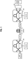
- the phase modulator to be calibrated according to the present invention is used in quantum key distribution devices, an example of which is illustrated in FIG. 1 .
- the phase modulator is installed in both the delay interferometers on the transmission and reception sides.
- the phase modulator is such that the phase modulation amount is to be controlled by a control signal.
- the phase modulator may be an LN phase modulator that performs phase modulation by an electrical signal utilizing the phenomenon that the refractive index of LiNbO 3 crystal varies according to an electric field.
- a phase modulator calibration method 1 includes: a delay interferometer providing step S1; a delay time synchronization step S2; a phase difference adjustment step S3; and a control signal determination step S4.
- the delay interferometer providing step S1 is a procedure to provide a first delay interferometer 10 and a second delay interferometer 20.
- a delay interferometer is a device that splits input light into two light rays at a one-to-one ratio and superimposes light having passed through a long optical path and light having passed through a short optical path to cause them to interfere with each other.
- the delay interferometer is, for example, a Mach-Zehnder interferometer, and has means for adjusting the optical path lengths. It is preferable that the delay interferometer be such that even when the phase of the input light is changed with a short cycle, the variation in the phase difference between the light having passed through the long optical path and the light having passed through the short optical path is small. For this reason, an example of the implementation of a delay interferometer is to use, for example, an asymmetric interferometer using a planar lightwave circuit (hereinafter abbreviated as PLC) using quartz as the optical path and use temperature adjustment means for adjusting the optical path length.
- PLC planar lightwave circuit
- the first delay interferometer 10 has a short optical path 13A and a long optical path 13B, and has rough adjustment means 14A and fine adjustment means 14B as adjustment means for optical path length.
- the rough adjustment means 14A is a mechanical adjustment such as one using a screw or the like.
- the fine adjustment means 14B is an adjustment using a piezoelectric element or the like, or an adjustment using expansion and contraction due to changes in the temperature of the substance forming the optical path.
- the first delay interferometer 10 has input terminals 11A and 11B and output terminals 12a and 12B.
- the phase modulator calibration method 1 uses one input terminal, e.g., 11A.
- one output terminal e.g., 12A
- both the output terminals may be used.
- the output from the two output terminals 12A and 12B when, for example, the phase difference between the light having passed through the short optical path 13A and the light having passed through the long optical path 13B is 0 degrees, the output is from the output terminal 12A; and when the phase difference is 180 degrees, the output is from the output terminal 12B.
- the first delay interferometer 10 serves as a phase calibration reference in the phase modulator calibration method 1. Considering this, a delay interferometer that permits fine adjustments to the optical path lengths while ensuring stability in the adjusted optical path lengths is the preferred choice.
- the second delay interferometer 20 includes a short optical path 23A in which a phase modulator 30 to be calibrated is installed.
- the phase modulator 30 has a control signal input terminal 31 that allows control of the phase modulation amount form outside the second delay interferometer 20.
- the second delay interferometer 20 at least includes rough adjustment means 24A and may include fine adjustment means.
- the delay time synchronization step S2 is a procedure to synchronize the delay times of the first and second delay interferometers 10 and 20 with the cycle of the transmission clock.
- a phase state is set at every cycle of the transmission clock. Synchronizing the delay time of the delay interferometer with the cycle of the transmission clock enables the measurement of interference between light in adjacent time slots.
- the delay time synchronization step S2 is performed by measuring the delay times of the delay interferometers and adjusting the optical path lengths.
- the delay time is measured by inputting pulse laser light to a delay interferometer and by measuring a time interval between pulses split from one input pulse.
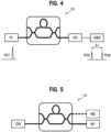
- a pulse laser PL is connected to one input terminal of the first delay interferometer 10
- a photodetector PD is connected to one output terminal, and the waveform is measured by an oscilloscope OSC.
- the step involves measuring the time interval ⁇ t between pulses P02 and P03 and adjusting the optical path length difference between the short optical path and the long optical path of the first delay interferometer 10 so that the time interval ⁇ t becomes identical to the cycle of the transmission clock.
- the adjustment of the optical path lengths may be performed by the rough adjustment means.
- the range of adjustment is expected to be 0.1 mm to 10 mm.
- the phase difference adjustment step S3 is a procedure for the first delay interferometer 10, which is used as the phase calibration reference, to adjust the phase difference so that the input light causes an intensity-enhancing interference on the output.
- the wavelength of the input light is the wavelength of signal light used in the optical communication path, e.g., an optical fiber, connecting the transmission side and the reception side.
- An example of such wavelength is 1.55 ⁇ m.
- the phase difference meant in the phase difference adjustment step S3 means the phase difference between the light having passed through the short optical path and the light having passed through the long optical path and varies based on the difference between the optical path length of the short optical path and the optical path length of the long optical path.
- the phase difference adjustment step S3 is performed by adjusting the optical path length so that the intensity of the light at the output of the delay interferometer is maximized.
- the phase difference adjustment step S3 involves, as the example illustrated in FIG. 5 , connecting a continuous-wave laser CW to one input terminal of the first delay interferometer 10 and a power meter M1 to one output terminal, and performing adjustment to obtain an optical path length showing a maximum value.
- the interference clarity expressed as (Vmax - Vmin) / (Vmax + Vmin) serves as an indicator of the presence of sufficient interference. Interference clarity enables measures, for example, to check the calibration system if a certain level of interference clarity is not ensured.
- the extinction ratio is given by 10•log(Vmax/Vmin).
- the phase difference adjustment step S3 performs adjustment of optical path length by the fine adjustment means. For example, when the wavelength of the signal light is 1.55 ⁇ m and when the refractive index of the optical path of the delay interferometer is 1.5, the optical path length corresponding to 360-degree phase difference is approximately 1 ⁇ m. Therefore, to control the phase with an accuracy of less than 4 degrees, an adjustment of about 10 nm is required. This adjustment can be achieved, for instance, through the use of a piezoelectric element or temperature control. The adjustment through the use of temperature control is preferred because it enables particularly fine adjustment.
- the subsequent procedures are conducted using the first delay interferometer 10 to which the phase difference adjustment step S3 has been applied as the reference for phase calibration.
- the control signal determination step S4 is a procedure to determine the value of the control signal corresponding to a phase modulation amount for the phase modulator to be calibrated. To be more precise, the correspondence relationship between the phase modulation amount and the control signal varies among individual phase modulators. Determining the control signal value corresponding to the phase modulation amount for each phase modulator enables calibration of the phase modulator. It is possible to observe the phase modulation amount by causing an interference of light.
- the control signal determination step S4 is performed using a calibration circuitry 100, which is, as illustrated in FIG. 6 , formed by connecting in a cascaded manner the first delay interferometer 10, having undergone the phase difference adjustment step S3, as the front stage to the second delay interferometer 20, having undergone the delay time synchronization step S2, as the rear stage.
- the phase modulator 30 is installed in the short optical path of the second delay interferometer 20.
- the second delay interferometer 20 is preferably a PLC or the like and, when polarization dependency is a matter of concern, it is preferable that the calibration circuitry 100 have a polarization filter 50 in front of the input terminal of the second delay interferometer 20.
- the control signal determination step S4 involves connecting the pulse laser PL to the input terminal of the front stage 10 of the calibration circuitry 100 and connecting the photodetector PD to the output terminal of the rear stage 20 to measure the waveform by the oscilloscope OSC.
- a control signal generator 40 is connected to the phase modulator 30.
- the control signal generator 40 is a device that generates a voltage signal for controlling the phase modulator 30.
- the pulse P11 inputted is split into two pulses P12 and P13 by the front stage 10 and then the two pulses P12 and P13 are each split into two pulses by the rear stage 20.
- the delay time of the front stage 10 and the delay time of the rear stage 20 are each ⁇ t, three pulses P14, P15, and P16 with time intervals ⁇ t are outputted from the rear stage 20.
- the central pulse P15 is positioned at the midpoint between the leading pulse P14 and the trailing pulse P16.
- the intensity of the central pulse P15 corresponds to the phase modulation amount of the phase modulator 30.
- Quantum key distribution requires control signal values that produce a phase modulation amount of 0 degrees and a phase modulation amount of 180 degrees. Accordingly, the central pulse P15 is measured while adjusting the control signal by the control signal generator 40. The intensity of the central pulse P15 is maximized by an intensity-enhancing interference when the phase modulation amount is 0 degrees and is minimized by an intensity-diminishing interference when the phase modulation amount is 180 degrees. In view of this, a control signal that produces a maximum intensity of the central pulse P15 is determined as 0-degree control signal and a control signal that produces a minimum intensity of the central pulse P15 is determined as 180-degree control signal.
- control signal determination step S4 values of the control signals corresponding to the 0- and 180-degree phase modulation amounts are determined, completing the calibration of the phase modulator.
- the balanced photodetector to be calibrated according to the present invention has a pair of input terminals.
- a balanced photodetector 60 is, for example, as illustrated in FIG. 1 , a device connected to a delay interferometer of a quantum key distribution device on the reception side and configured to convert the difference between light intensities at the two input terminals into an electrical signal to be outputted.
- the electrical signal outputted is inputted to an AD converter of a signal processing device.
- the balanced photodetector calibration method 2 includes, as illustrated in FIG. 2B , a delay interferometer providing step S 1, a delay time synchronization step S2, a phase difference adjustment step S3, a control signal determination step S4, and a photodetector adjustment step S5.
- a delay interferometer providing step S 1 a delay time synchronization step S2
- a phase difference adjustment step S3 a control signal determination step S4
- steps from the delay interferometer providing step S 1 to the control signal determination step S4 are common to those in the phase modulator calibration method 1 already described, the description thereof is omitted.
- the photodetector adjustment step S5 is a procedure to adjust the balanced photodetector so that it operates without a bias.
- the balanced photodetector is capable of outputting a difference between the intensities of a pair of input light rays as an electrical signal. Accordingly, the photodetector is to be adjusted so that the magnitude of the electrical signal generated for light rays having the same intensity does not fluctuate between the input terminals.
- the photodetector adjustment step S5 is conducted based on the optical signals to which phase modulation has been applied by the calibrated phase modulator 30.
- the balanced photodetector 60 has, for example, as illustrated in FIG. 7 : a pair of photodiodes 62A and 62B; optical attenuators 61A and 61B; and an amplifier 65.
- the pair of input light rays is incident upon the pair of photodiodes 62A and 62B via the optical attenuators 61A and 61B.
- the optical currents of the pair of photodiodes 62A and 62B are input to the amplifier 65 that converts currents to a voltage, resulting in an output of a voltage corresponding to the difference between the optical currents from the output terminal 66.
- the photodetector adjustment step S5 is conducted with the continuous-wave laser CW connected to the input terminal of the front stage 10 of the calibration circuitry 100 and the balanced photodetector 60 connected to the output terminals of the rear stage 20 of the calibration circuitry 100.
- the wavelength of the input continuous-wave laser light is the same as the wavelength of the continuous-wave laser light used in the phase difference adjustment step S3.
- the output of the balanced photodetector 60 may be measured, for example, as a voltage waveform with an oscilloscope.
- the control signal generator 40 is connected to the phase modulator 30.
- the control signal generator 40 is set to alternately repeat the 0-degree control signal and 180-degree control signal determined with the phase modulator calibration method 1.
- the repeat frequency is the frequency of the transmission clock, for example.
- the two outputs of the rear stage 20 are such that one is intensity-enhanced and the other is intensity-diminished.
- the 180-degree control signal is fed, the two outputs are such that the one is intensity-diminished and the other is intensity-enhanced.
- the two outputs of the rear stage 20 produce opposite-phase light rays that vary in the same intensity range.
- the adjustment is conducted so that the balanced photodetector 60 operates for these output light rays without a bias.
- the amplitude of the output voltage is maximized.
- the gains of the balanced photodetector 60 for the pair of input terminals are each adjusted so that the amplitude of the output voltage is maximized. It is preferable to further measure the extinction ratio and adjust the gains of the balanced photodetector 60 so that the extinction ratio at the rear stage 20 is maximized.
- the adjustment of the gains may be performed based on the attenuation amount of the optical attenuators 61A and 61B or with internal resistive elements or the like of the amplifier 65.
- phase modulator 30 and/or the balanced photodetector 60 are used in a quantum key distribution device and may deviate from its calibrated state. Therefore, it is preferable to determine an interval of days or the like for example and periodically perform calibration using the phase modulator calibration method 1 and the balanced photodetector calibration method 2.
- a phase modulator calibration system 3 calibrates a phase modulator whose phase modulation amount is controlled by a control signal.
- the phase modulator is an LN phase modulator, for example.
- the phase modulator calibration system 3 includes, as illustrated in FIG. 8 , a calibration circuitry 100, a light source 70, a photodetector 80, and a control signal generator 40.
- the calibration circuitry 100 includes the first delay interferometer 10 and the second delay interferometer 20, which are connected in cascade as the front stage and the rear stage, respectively.
- the first delay interferometer 10 has been adjusted so that the delay time is synchronized with the cycle of the transmission clock and the phase difference produces an intensity-enhancing interference.
- the second delay interferometer 20 the delay time is synchronized with the cycle of the transmission clock and the phase modulator 30 to be calibrated is installed in an optical path.
- the calibration circuitry 100 have a polarization filter 50 in front of the rear stage 20 when polarization dependency of the rear stage 20 is a matter of concern.
- the first and second delay interferometers 10 and 20, the phase modulator 30, and the control signal generator 40 are as described already.
- the light source 70 is, for example, a pulse laser or a continuous-wave laser.
- the photodetector 80 outputs a current or voltage corresponding to the intensity of light and may be connected to both or one of the two outputs of the rear stage 20.
- the phase modulator calibration method 1 is a method of calibrating a phase modulator whose phase modulation amount is controlled by a control signal, the method including steps of: providing (S 1) a first delay interferometer 10 to be used as a phase calibration reference and a second delay interferometer 20 in which a phase modulator 30 to be calibrated is installed in an optical path; for each of the first and second delay interferometers 10 and 20, measuring a delay time based on a time interval between pulses split from one input pulse and synchronizing (S2) the delay time with the cycle of the transmission clock; for the first delay interferometer 10, adjusting (S3) the phase difference so that the input continuous-wave laser light produces an intensity-enhancing interference at the output; and determining (S4) the control signal with a calibration circuitry 100 formed by connecting the first delay interferometer 10 as a front stage and the second delay interferometer 20 as a rear stage in a cascaded manner.
- the phase modulator calibration method 1 uses the first delay interferometer 10, which has been adjusted so that the phase difference caused by the optical path difference is 0 degree (including integer multiples of 360 degrees), as the calibration reference. This makes it possible to ensure that the phase modulation amount by the calibrated phase modulator 30 is a correct value as an absolute phase.
- the adjustment of the phase difference of the first delay interferometer 10 is performed using continuous light. This allows the first delay interferometer 10, which is used as the phase calibration reference, to be accurately adjusted in an easy manner.
- the phase modulator calibration method 1 allows the calibration to be performed using before-attenuation, strong optical pulses or continuous light, rather than using weak light originally required for quantum key distribution. Accordingly, accuracy of the calibration is increased, and the calibration is performed with respect to the absolute phase with high accuracy even when the frequency of the transmission clock is high. As a result, provision of the accurately calibrated phase modulator to both the transmission and reception sides of quantum key distribution increases the implementation security of the quantum key distribution devices.
- the adjustment step S3 for adjusting the phase difference of the first delay interferometer 10 is preferably conducted by adjusting the temperature of the first delay interferometer 10.
- the phase modulator calibration method 1 accurately performs the adjustment of the phase difference of the first delay interferometer 10.
- the adjustment step S3 for adjusting the phase difference of the first delay interferometer 10 is preferably conducted by measuring the extinction ratio at the output and performing the adjustment so that the extinction ratio is maximized.
- the phase modulator calibration method 1 further accurately performs the adjustment of the phase difference of the first delay interferometer 10.
- control signal determination step S4 includes: while inputting pulse laser light into an input of the front stage 10 and measuring the intensity of a central pulse positioned at the midpoint between a leading pulse and a trailing pulse split from one pulse and outputted from the rear stage 20, adjusting a control signal to determine a control signal that produces a maximum intensity of the central pulse as a 0-degree control signal and to determine a control signal that produces a minimum intensity of the central pulse as a 180-degree control signal.
- phase modulator calibration method 1 performs accurate calibration in a clarified, easy-to-understand manner.
- the balanced photodetector calibration method 2 includes: in the calibration circuitry 100 in which the phase modulator 30 has been calibrated according to the phase modulator calibration method 1, inputting continuous-wave laser light into an input of the front stage 10 and alternately repeating the 0-degree control signal and the 180-degree control signal to control the phase modulator 30; and adjusting a gain of the balanced photodetector 60 connected to the rear stage 20 so that the extinction ratio measured by the balanced photodetector 60 is maximized.
- the balanced photodetector calibration method 2 calibrates the balanced photodetector 60 as well with high accuracy using the calibrated first delay interferometer 10 and the calibrated phase modulator 30 as a calibration reference. With this, the implementation security of quantum key distribution is further increased.
- phase modulator and balanced photodetector calibrated by the phase modulator calibration method 1 and balanced photodetector calibration method 2 ensures the implementation security of quantum key distribution and makes it possible to determine whether the quantum key distribution device is correctly implemented.
- the phase modulator calibration system is a calibration system of a phase modulator whose phase modulation amount is controlled by a control signal, the calibration system including: a calibration circuitry 100; a light source 70 configured to input light to the calibration circuitry 100; a photodetector 80 connected to an output of the calibration circuitry 100; and a control signal generator 40 configured to generate a control signal.
- the calibration circuitry 100 includes: a first delay interferometer 10, which has been adjusted so that a delay time has been synchronized with a cycle of the transmission clock and a phase difference has been adjusted to produce an intensity-enhancing interference; and a second delay interferometer 20, in which a phase modulator 30 to be calibrated is installed in an optical path.
- the first delay interferometer 10 and the second delay interferometer 20 are connected in cascade as a front stage and a rear stage, respectively.
- the phase modulator calibration system 3 calibrates the phase modulator 30 with high accuracy using the first delay interferometer 10 as a phase calibration reference. Moreover, the phase modulator calibration system 3 enables verification of the operation of the phase modulator. With this, it is possible to determine whether the quantum key distribution device is correctly implemented.
- the delay interferometer may be, in addition to PLC, one in which the optical path is a space or optical fiber and the optical system is constructed using half mirrors or the like.
- the phase modulator 30 may be installed in the long optical path 23B rather than the short optical path 23A.
- the installation of the phase modulator 30 in the second delay interferometer 20 may be performed after performing the delay time synchronization step S2.
- the adjustment step S3 of adjusting phase difference of the first delay interferometer 10 may be performed by inserting a dielectric near the optical path and varying the voltage applied to the dielectric.
- power meters M1 and M2 may be connected to the two output terminals to measure the intensities of the light.
- the photodetector PD and the oscilloscope OSC may be connected for measurement as illustrated in FIG. 4 .
- phase modulator calibration system 3 functions as a balanced photodetector calibration system to calibrate the balanced photodetector 60 with high accuracy.
Landscapes
- Physics & Mathematics (AREA)
- Nonlinear Science (AREA)
- Optics & Photonics (AREA)
- General Physics & Mathematics (AREA)
- Electromagnetism (AREA)
- Engineering & Computer Science (AREA)
- Computer Networks & Wireless Communication (AREA)
- Signal Processing (AREA)
- Optical Communication System (AREA)
- Investigating Or Analysing Materials By Optical Means (AREA)
- Optical Modulation, Optical Deflection, Nonlinear Optics, Optical Demodulation, Optical Logic Elements (AREA)
Abstract
Description
- The present invention relates to, in relation to quantum key distribution, a calibration method for phase modulator, a calibration method for balanced photodetector, and a calibration system for phase modulator.
- Quantum key distribution is a technique that enables the sharing of information-theoretically secure cryptographic keys (random number sequences) with remote locations. Its security is theoretically guaranteed by the laws of physics. However, it is based on the assumption that the actual operation of the communication equipment does not deviate significantly from the theoretical operation.
- In the field of quantum key distribution, research is underway to achieve higher speed and wider bandwidth with a method using the phase state of light. This method causes the phase state of light to map to the bit values of the information and performs phase modulation to the optical signal for transmission and reception. The phase modulation is a technique used for high-speed optical communication. The phase accuracy required for quantum key distribution significantly differs from the phase accuracy required for optical communication. For example, Non-Patent Literature 1 points out the importance of phase accuracy in the components that make up a quantum key distribution device.
- Non-Patent Literature: M. Pereira, M. Curtty, and K. Tamaki, "Quantum key distribution with flawed and leaky source", npj Quantum Information, volume 5, Article number: 62 (2019)
- In the case of optical communication, as digital processing is feasible, communication is possible without problems even if there is an error of 10-20 degrees in the phase of the optical signal. On the other hand, quantum key distribution requires the phase of an optical wave with less than one photon per pulse be established with a few degrees of accuracy. Simply controlling the phase based on the state measured by a photodetector does not ensure the absolute phase accuracy required for quantum key distribution. Therefore, in the field of quantum key distribution, there is a need for a technique that ensures the measured phase has absolute phase accuracy.
- The present invention has been made to solve such problems and is aimed at providing a high-accurate method of calibrating a phase modulator, a high-accurate method of calibrating a balanced photodetector, and a high-accurate calibration system for calibrating the phase modulator, to ensure quantum state control with the accuracy required for quantum key distribution.
- To solve the problem, a phase modulator calibration method according to the invention is a phase modulator calibration method of calibrating a phase modulator whose phase modulation amount is controlled by a control signal, the method including steps of: providing a first delay interferometer to be used as a phase calibration reference and a second delay interferometer in which a phase modulator to be calibrated is installed in an optical path; for each of the first and second delay interferometers, measuring a delay time based on a time interval between pulses split from one input pulse and synchronizing the delay time with a cycle of a transmission clock; for the first delay interferometer, adjusting a phase difference so that input continuous-wave laser light produces an intensity-enhancing interference at an output; and determining the control signal with a calibration circuitry formed by connecting the first delay interferometer as a front stage and the second delay interferometer as a rear stage in a cascaded manner.
- A phase modulator calibration system according to the present invention is a calibration system of a phase modulator whose phase modulation amount is controlled by a control signal, the calibration system including: a calibration circuitry; a light source configured to input light to the calibration circuitry; a photodetector connected to an output of the calibration circuitry; and a control signal generator configured to generate the control signal, wherein the calibration circuitry comprises: a first delay interferometer, which has been adjusted so that a delay time is synchronized with a cycle of a transmission clock and a phase difference produces an intensity-enhancing interference; and a second delay interferometer, in which a phase modulator to be calibrated is installed in an optical path, and wherein the first delay interferometer and the second delay interferometer are connected in cascade as a front stage and a rear stage, respectively.
- The present invention makes it possible to calibrate a phase modulator and a balanced photodetector with high accuracy to ensure the quantum state control with the accuracy required for quantum key distribution, and to provide a phase modulator calibration system capable of performing high-accurate calibration.
-
-
FIG. 1 is a schematic diagram illustrating an example of a quantum key distribution device. -
FIG. 2A is a flowchart illustrating an example of a phase modulator calibration method according to an embodiment. -
FIG. 2B is a flowchart illustrating an example of a balanced photodetector calibration method according to an embodiment. -
FIG. 3A is a schematic diagram of a first delay interferometer. -
FIG. 3B is a schematic diagram of a second delay interferometer in which a phase modulator to be calibrated is installed. -
FIG. 4 is a schematic diagram illustrating an example of a circuitry with which the delay time of a delay interferometer is measured. -
FIG. 5 is a schematic diagram illustrating an example of a circuitry with which the phase difference of a delay interferometer is measured. -
FIG. 6 is a schematic diagram illustrating an example of a calibration circuitry according to an embodiment. -
FIG. 7 is a schematic diagram illustrating an example of a calibration circuitry of a balanced photodetector. -
FIG. 8 is a schematic diagram illustrating an example of a phase modulator calibration system according to an embodiment. - A phase modulator calibration method according to the present invention will be described with reference to the drawings. The phase modulator to be calibrated according to the present invention is used in quantum key distribution devices, an example of which is illustrated in
FIG. 1 . The phase modulator is installed in both the delay interferometers on the transmission and reception sides. - The phase modulator is such that the phase modulation amount is to be controlled by a control signal. The phase modulator may be an LN phase modulator that performs phase modulation by an electrical signal utilizing the phenomenon that the refractive index of LiNbO3 crystal varies according to an electric field.
- As illustrated in
FIG. 2A , a phase modulator calibration method 1 according to the present invention includes: a delay interferometer providing step S1; a delay time synchronization step S2; a phase difference adjustment step S3; and a control signal determination step S4. - The delay interferometer providing step S1 is a procedure to provide a
first delay interferometer 10 and asecond delay interferometer 20. A delay interferometer is a device that splits input light into two light rays at a one-to-one ratio and superimposes light having passed through a long optical path and light having passed through a short optical path to cause them to interfere with each other. - The delay interferometer is, for example, a Mach-Zehnder interferometer, and has means for adjusting the optical path lengths. It is preferable that the delay interferometer be such that even when the phase of the input light is changed with a short cycle, the variation in the phase difference between the light having passed through the long optical path and the light having passed through the short optical path is small. For this reason, an example of the implementation of a delay interferometer is to use, for example, an asymmetric interferometer using a planar lightwave circuit (hereinafter abbreviated as PLC) using quartz as the optical path and use temperature adjustment means for adjusting the optical path length.
- As the example illustrated in
FIG. 3A , thefirst delay interferometer 10 has a shortoptical path 13A and a longoptical path 13B, and has rough adjustment means 14A and fine adjustment means 14B as adjustment means for optical path length. The rough adjustment means 14A is a mechanical adjustment such as one using a screw or the like. The fine adjustment means 14B is an adjustment using a piezoelectric element or the like, or an adjustment using expansion and contraction due to changes in the temperature of the substance forming the optical path. - The
first delay interferometer 10 hasinput terminals output terminals 12a and 12B. The phase modulator calibration method 1 uses one input terminal, e.g., 11A. Regarding the output terminal, one output terminal, e.g., 12A, is used. However, both the output terminals may be used. Regarding the output from the twooutput terminals optical path 13A and the light having passed through the longoptical path 13B is 0 degrees, the output is from theoutput terminal 12A; and when the phase difference is 180 degrees, the output is from theoutput terminal 12B. - The
first delay interferometer 10 serves as a phase calibration reference in the phase modulator calibration method 1. Considering this, a delay interferometer that permits fine adjustments to the optical path lengths while ensuring stability in the adjusted optical path lengths is the preferred choice. - As illustrated in
FIG. 3B , thesecond delay interferometer 20 includes a shortoptical path 23A in which aphase modulator 30 to be calibrated is installed. Thephase modulator 30 has a control signal input terminal 31 that allows control of the phase modulation amount form outside thesecond delay interferometer 20. Thesecond delay interferometer 20 at least includes rough adjustment means 24A and may include fine adjustment means. - Note that in some cases illustration of the rough adjustment means, fine adjustment means, and control input terminal in the drawings may be omitted.
- The delay time synchronization step S2 is a procedure to synchronize the delay times of the first and
second delay interferometers - In the case of the quantum key distribution according to the present invention, a phase state is set at every cycle of the transmission clock. Synchronizing the delay time of the delay interferometer with the cycle of the transmission clock enables the measurement of interference between light in adjacent time slots.
- The delay time synchronization step S2 is performed by measuring the delay times of the delay interferometers and adjusting the optical path lengths. The delay time is measured by inputting pulse laser light to a delay interferometer and by measuring a time interval between pulses split from one input pulse. When measuring the delay time of the
first delay interferometer 10, as the example illustrated inFIG. 4 , a pulse laser PL is connected to one input terminal of thefirst delay interferometer 10, a photodetector PD is connected to one output terminal, and the waveform is measured by an oscilloscope OSC. When an input pulse P01 is split and outputted as two pulses P02 and P03, the step involves measuring the time interval Δt between pulses P02 and P03 and adjusting the optical path length difference between the short optical path and the long optical path of thefirst delay interferometer 10 so that the time interval Δt becomes identical to the cycle of the transmission clock. - In the delay time synchronization step S2, the adjustment of the optical path lengths may be performed by the rough adjustment means. For example, when the frequency of the transmission clock is 1 GHz and a delay interferometer whose delay time has been set to 1 ns in advance is available, the range of adjustment is expected to be 0.1 mm to 10 mm.
- The same procedure is also applied to the
second delay interferometer 20. Then, using the first andsecond interferometers - The phase difference adjustment step S3 is a procedure for the
first delay interferometer 10, which is used as the phase calibration reference, to adjust the phase difference so that the input light causes an intensity-enhancing interference on the output. In the phase difference adjustment step S3, the wavelength of the input light is the wavelength of signal light used in the optical communication path, e.g., an optical fiber, connecting the transmission side and the reception side. An example of such wavelength is 1.55 µm. - The phase difference meant in the phase difference adjustment step S3 means the phase difference between the light having passed through the short optical path and the light having passed through the long optical path and varies based on the difference between the optical path length of the short optical path and the optical path length of the long optical path. When the input light causes an intensity-enhancing interference at the output, the intensity of the light at the output is maximized. In view of this, the phase difference adjustment step S3 is performed by adjusting the optical path length so that the intensity of the light at the output of the delay interferometer is maximized.
- The phase difference adjustment step S3 involves, as the example illustrated in
FIG. 5 , connecting a continuous-wave laser CW to one input terminal of thefirst delay interferometer 10 and a power meter M1 to one output terminal, and performing adjustment to obtain an optical path length showing a maximum value. - When the maximum and minimum output values of the power meter M1 are denoted as Vmax and Vmin respectively, the interference clarity expressed as (Vmax - Vmin) / (Vmax + Vmin) serves as an indicator of the presence of sufficient interference. Interference clarity enables measures, for example, to check the calibration system if a certain level of interference clarity is not ensured.
- It is possible to further measure the extinction ratio, in the vicinity of the maximum value Vmax. Performing the adjustment to maximize the extinction ratio allows for a more precise adjustment of the optical path length. The extinction ratio is given by 10•log(Vmax/Vmin).
- The phase difference adjustment step S3 performs adjustment of optical path length by the fine adjustment means. For example, when the wavelength of the signal light is 1.55 µm and when the refractive index of the optical path of the delay interferometer is 1.5, the optical path length corresponding to 360-degree phase difference is approximately 1 µm. Therefore, to control the phase with an accuracy of less than 4 degrees, an adjustment of about 10 nm is required. This adjustment can be achieved, for instance, through the use of a piezoelectric element or temperature control. The adjustment through the use of temperature control is preferred because it enables particularly fine adjustment.
- The subsequent procedures are conducted using the
first delay interferometer 10 to which the phase difference adjustment step S3 has been applied as the reference for phase calibration. - The control signal determination step S4 is a procedure to determine the value of the control signal corresponding to a phase modulation amount for the phase modulator to be calibrated. To be more precise, the correspondence relationship between the phase modulation amount and the control signal varies among individual phase modulators. Determining the control signal value corresponding to the phase modulation amount for each phase modulator enables calibration of the phase modulator. It is possible to observe the phase modulation amount by causing an interference of light.
- The control signal determination step S4 is performed using a
calibration circuitry 100, which is, as illustrated inFIG. 6 , formed by connecting in a cascaded manner thefirst delay interferometer 10, having undergone the phase difference adjustment step S3, as the front stage to thesecond delay interferometer 20, having undergone the delay time synchronization step S2, as the rear stage. Thephase modulator 30 is installed in the short optical path of thesecond delay interferometer 20. In thecalibration circuitry 100, thesecond delay interferometer 20 is preferably a PLC or the like and, when polarization dependency is a matter of concern, it is preferable that thecalibration circuitry 100 have apolarization filter 50 in front of the input terminal of thesecond delay interferometer 20. - The control signal determination step S4 involves connecting the pulse laser PL to the input terminal of the
front stage 10 of thecalibration circuitry 100 and connecting the photodetector PD to the output terminal of therear stage 20 to measure the waveform by the oscilloscope OSC. Acontrol signal generator 40 is connected to thephase modulator 30. Thecontrol signal generator 40 is a device that generates a voltage signal for controlling thephase modulator 30. - As the example illustrated in
FIG. 6 , the pulse P11 inputted is split into two pulses P12 and P13 by thefront stage 10 and then the two pulses P12 and P13 are each split into two pulses by therear stage 20. As the delay time of thefront stage 10 and the delay time of therear stage 20 are each Δt, three pulses P14, P15, and P16 with time intervals Δt are outputted from therear stage 20. The central pulse P15 is positioned at the midpoint between the leading pulse P14 and the trailing pulse P16. The intensity of the central pulse P15 corresponds to the phase modulation amount of thephase modulator 30. - Quantum key distribution requires control signal values that produce a phase modulation amount of 0 degrees and a phase modulation amount of 180 degrees. Accordingly, the central pulse P15 is measured while adjusting the control signal by the
control signal generator 40. The intensity of the central pulse P15 is maximized by an intensity-enhancing interference when the phase modulation amount is 0 degrees and is minimized by an intensity-diminishing interference when the phase modulation amount is 180 degrees. In view of this, a control signal that produces a maximum intensity of the central pulse P15 is determined as 0-degree control signal and a control signal that produces a minimum intensity of the central pulse P15 is determined as 180-degree control signal. - Through the control signal determination step S4, values of the control signals corresponding to the 0- and 180-degree phase modulation amounts are determined, completing the calibration of the phase modulator.
- Next, description will be given of a balanced photodetector calibration method according to the present invention. The balanced photodetector to be calibrated according to the present invention has a pair of input terminals. A
balanced photodetector 60 is, for example, as illustrated inFIG. 1 , a device connected to a delay interferometer of a quantum key distribution device on the reception side and configured to convert the difference between light intensities at the two input terminals into an electrical signal to be outputted. The electrical signal outputted is inputted to an AD converter of a signal processing device. - The balanced
photodetector calibration method 2 according to the present invention includes, as illustrated inFIG. 2B , a delay interferometer providing step S 1, a delay time synchronization step S2, a phase difference adjustment step S3, a control signal determination step S4, and a photodetector adjustment step S5. As the steps from the delay interferometer providing step S 1 to the control signal determination step S4 are common to those in the phase modulator calibration method 1 already described, the description thereof is omitted. - The photodetector adjustment step S5 is a procedure to adjust the balanced photodetector so that it operates without a bias. The balanced photodetector is capable of outputting a difference between the intensities of a pair of input light rays as an electrical signal. Accordingly, the photodetector is to be adjusted so that the magnitude of the electrical signal generated for light rays having the same intensity does not fluctuate between the input terminals. The photodetector adjustment step S5 is conducted based on the optical signals to which phase modulation has been applied by the calibrated
phase modulator 30. - The
balanced photodetector 60 has, for example, as illustrated inFIG. 7 : a pair ofphotodiodes optical attenuators amplifier 65. The pair of input light rays is incident upon the pair ofphotodiodes optical attenuators photodiodes amplifier 65 that converts currents to a voltage, resulting in an output of a voltage corresponding to the difference between the optical currents from theoutput terminal 66. - The photodetector adjustment step S5 is conducted with the continuous-wave laser CW connected to the input terminal of the
front stage 10 of thecalibration circuitry 100 and thebalanced photodetector 60 connected to the output terminals of therear stage 20 of thecalibration circuitry 100. The wavelength of the input continuous-wave laser light is the same as the wavelength of the continuous-wave laser light used in the phase difference adjustment step S3. The output of thebalanced photodetector 60 may be measured, for example, as a voltage waveform with an oscilloscope. Thecontrol signal generator 40 is connected to thephase modulator 30. - The
control signal generator 40 is set to alternately repeat the 0-degree control signal and 180-degree control signal determined with the phase modulator calibration method 1. The repeat frequency is the frequency of the transmission clock, for example. When the 0-degree control signal is fed, the two outputs of therear stage 20 are such that one is intensity-enhanced and the other is intensity-diminished. Conversely, when the 180-degree control signal is fed, the two outputs are such that the one is intensity-diminished and the other is intensity-enhanced. Thus, the two outputs of therear stage 20 produce opposite-phase light rays that vary in the same intensity range. - The adjustment is conducted so that the
balanced photodetector 60 operates for these output light rays without a bias. When thebalanced photodetector 60 operates without a bias, the amplitude of the output voltage is maximized. In view of this, the gains of thebalanced photodetector 60 for the pair of input terminals are each adjusted so that the amplitude of the output voltage is maximized. It is preferable to further measure the extinction ratio and adjust the gains of thebalanced photodetector 60 so that the extinction ratio at therear stage 20 is maximized. The adjustment of the gains may be performed based on the attenuation amount of theoptical attenuators amplifier 65. - The
phase modulator 30 and/or thebalanced photodetector 60 are used in a quantum key distribution device and may deviate from its calibrated state. Therefore, it is preferable to determine an interval of days or the like for example and periodically perform calibration using the phase modulator calibration method 1 and the balancedphotodetector calibration method 2. - Next, description will be given of a phase modulator calibration system according to the present invention. A phase modulator calibration system 3 calibrates a phase modulator whose phase modulation amount is controlled by a control signal. The phase modulator is an LN phase modulator, for example.
- The phase modulator calibration system 3 includes, as illustrated in
FIG. 8 , acalibration circuitry 100, alight source 70, aphotodetector 80, and acontrol signal generator 40. Thecalibration circuitry 100 includes thefirst delay interferometer 10 and thesecond delay interferometer 20, which are connected in cascade as the front stage and the rear stage, respectively. Thefirst delay interferometer 10 has been adjusted so that the delay time is synchronized with the cycle of the transmission clock and the phase difference produces an intensity-enhancing interference. In thesecond delay interferometer 20, the delay time is synchronized with the cycle of the transmission clock and thephase modulator 30 to be calibrated is installed in an optical path. It is preferable that thecalibration circuitry 100 have apolarization filter 50 in front of therear stage 20 when polarization dependency of therear stage 20 is a matter of concern. - The first and
second delay interferometers phase modulator 30, and thecontrol signal generator 40 are as described already. Thelight source 70 is, for example, a pulse laser or a continuous-wave laser. Thephotodetector 80 outputs a current or voltage corresponding to the intensity of light and may be connected to both or one of the two outputs of therear stage 20. - The phase modulator calibration method 1 according to the present invention is a method of calibrating a phase modulator whose phase modulation amount is controlled by a control signal, the method including steps of: providing (S 1) a
first delay interferometer 10 to be used as a phase calibration reference and asecond delay interferometer 20 in which aphase modulator 30 to be calibrated is installed in an optical path; for each of the first andsecond delay interferometers first delay interferometer 10, adjusting (S3) the phase difference so that the input continuous-wave laser light produces an intensity-enhancing interference at the output; and determining (S4) the control signal with acalibration circuitry 100 formed by connecting thefirst delay interferometer 10 as a front stage and thesecond delay interferometer 20 as a rear stage in a cascaded manner. - With such configuration, the phase modulator calibration method 1 uses the
first delay interferometer 10, which has been adjusted so that the phase difference caused by the optical path difference is 0 degree (including integer multiples of 360 degrees), as the calibration reference. This makes it possible to ensure that the phase modulation amount by the calibratedphase modulator 30 is a correct value as an absolute phase. In addition, the adjustment of the phase difference of thefirst delay interferometer 10 is performed using continuous light. This allows thefirst delay interferometer 10, which is used as the phase calibration reference, to be accurately adjusted in an easy manner. - The phase modulator calibration method 1 allows the calibration to be performed using before-attenuation, strong optical pulses or continuous light, rather than using weak light originally required for quantum key distribution. Accordingly, accuracy of the calibration is increased, and the calibration is performed with respect to the absolute phase with high accuracy even when the frequency of the transmission clock is high. As a result, provision of the accurately calibrated phase modulator to both the transmission and reception sides of quantum key distribution increases the implementation security of the quantum key distribution devices.
- The adjustment step S3 for adjusting the phase difference of the
first delay interferometer 10 is preferably conducted by adjusting the temperature of thefirst delay interferometer 10. - With such configuration, the phase modulator calibration method 1 accurately performs the adjustment of the phase difference of the
first delay interferometer 10. - The adjustment step S3 for adjusting the phase difference of the
first delay interferometer 10 is preferably conducted by measuring the extinction ratio at the output and performing the adjustment so that the extinction ratio is maximized. - With such configuration, the phase modulator calibration method 1 further accurately performs the adjustment of the phase difference of the
first delay interferometer 10. - It is preferable for the control signal determination step S4 to include: while inputting pulse laser light into an input of the
front stage 10 and measuring the intensity of a central pulse positioned at the midpoint between a leading pulse and a trailing pulse split from one pulse and outputted from therear stage 20, adjusting a control signal to determine a control signal that produces a maximum intensity of the central pulse as a 0-degree control signal and to determine a control signal that produces a minimum intensity of the central pulse as a 180-degree control signal. - With such configuration, the phase modulator calibration method 1 performs accurate calibration in a clarified, easy-to-understand manner.
- The balanced
photodetector calibration method 2 according to the present invention includes: in thecalibration circuitry 100 in which thephase modulator 30 has been calibrated according to the phase modulator calibration method 1, inputting continuous-wave laser light into an input of thefront stage 10 and alternately repeating the 0-degree control signal and the 180-degree control signal to control thephase modulator 30; and adjusting a gain of thebalanced photodetector 60 connected to therear stage 20 so that the extinction ratio measured by thebalanced photodetector 60 is maximized. - With such configuration, the balanced
photodetector calibration method 2 calibrates thebalanced photodetector 60 as well with high accuracy using the calibratedfirst delay interferometer 10 and the calibratedphase modulator 30 as a calibration reference. With this, the implementation security of quantum key distribution is further increased. - Using the phase modulator and balanced photodetector calibrated by the phase modulator calibration method 1 and balanced
photodetector calibration method 2 ensures the implementation security of quantum key distribution and makes it possible to determine whether the quantum key distribution device is correctly implemented. - The phase modulator calibration system according to the present invention is a calibration system of a phase modulator whose phase modulation amount is controlled by a control signal, the calibration system including: a
calibration circuitry 100; alight source 70 configured to input light to thecalibration circuitry 100; aphotodetector 80 connected to an output of thecalibration circuitry 100; and acontrol signal generator 40 configured to generate a control signal. Thecalibration circuitry 100 includes: afirst delay interferometer 10, which has been adjusted so that a delay time has been synchronized with a cycle of the transmission clock and a phase difference has been adjusted to produce an intensity-enhancing interference; and asecond delay interferometer 20, in which aphase modulator 30 to be calibrated is installed in an optical path. Thefirst delay interferometer 10 and thesecond delay interferometer 20 are connected in cascade as a front stage and a rear stage, respectively. - With such configuration, the phase modulator calibration system 3 calibrates the
phase modulator 30 with high accuracy using thefirst delay interferometer 10 as a phase calibration reference. Moreover, the phase modulator calibration system 3 enables verification of the operation of the phase modulator. With this, it is possible to determine whether the quantum key distribution device is correctly implemented. - Note that the delay interferometer may be, in addition to PLC, one in which the optical path is a space or optical fiber and the optical system is constructed using half mirrors or the like.
- In the
second delay interferometer 20, thephase modulator 30 may be installed in the longoptical path 23B rather than the shortoptical path 23A. In addition, the installation of thephase modulator 30 in thesecond delay interferometer 20 may be performed after performing the delay time synchronization step S2. - The adjustment step S3 of adjusting phase difference of the
first delay interferometer 10 may be performed by inserting a dielectric near the optical path and varying the voltage applied to the dielectric. In addition, power meters M1 and M2 may be connected to the two output terminals to measure the intensities of the light. Alternatively, rather than the power meters, the photodetector PD and the oscilloscope OSC may be connected for measurement as illustrated inFIG. 4 . - When a continuous-wave laser which emits light with the wavelength of light with which the phase difference of the
first delay interferometer 10 has been calibrated is used as thelight source 70 and abalanced photodetector 60 to be calibrated is used as thephotodetector 80, the phase modulator calibration system 3 functions as a balanced photodetector calibration system to calibrate thebalanced photodetector 60 with high accuracy. -
- 1: Calibration method (phase modulator)
- 2: Calibration method (balanced photodetector)
- 3: Calibration system (phase modulator)
- 10: First delay interferometer
- 20: Second delay interferometer
- 30: Phase modulator
- 31: Control signal input terminal
- 40: Control signal generator
- 50: Polarization filter
- 60: Balanced photodetector
- 70: Light source
- 80: Photodetector
- 100: Calibration circuitry
Claims (6)
- A phase modulator calibration method of calibrating a phase modulator whose phase modulation amount is controlled by a control signal, the method comprising steps of:providing a first delay interferometer to be used as a phase calibration reference and a second delay interferometer in which a phase modulator to be calibrated is installed in an optical path;for each of the first and second delay interferometers, measuring a delay time based on a time interval between pulses split from one input pulse and synchronizing the delay time with a cycle of a transmission clock;for the first delay interferometer, adjusting a phase difference so that input continuous-wave laser light produces an intensity-enhancing interference at an output; anddetermining the control signal with a calibration circuitry formed by connecting the first delay interferometer as a front stage and the second delay interferometer as a rear stage in a cascaded manner.
- The phase modulator calibration method according to claim 1,
wherein the step of adjusting the phase difference of the first delay interferometer is performed by adjusting a temperature of the first delay interferometer. - The phase modulator calibration method according to claim 1 or claim 2,
wherein the step of adjusting the phase difference of the first delay interferometer is performed by measuring an extinction ratio at the output and performing an adjustment so that the extinction ratio is maximized. - The phase modulator calibration method according to any one of claims 1 to 3,
wherein the step of determining the control signal comprises:
while inputting pulse laser light into an input of the front stage and measuring an intensity of a central pulse positioned at a midpoint between a leading pulse and a trailing pulse split from one pulse and outputted from the rear stage, adjusting the control signal to determine a control signal that produces a maximum intensity of the central pulse as a 0-degree control signal and to determine a control signal that produces a minimum intensity of the central pulse as a 180-degree control signal. - A balanced photodetector calibration method comprising steps of, in the calibration circuitry in which the phase modulator has been calibrated by the phase modulator calibration method according to any one of claims 1 to 4:inputting the continuous-wave laser light to the input of the front stage and alternately repeating the 0-degree control signal and the 180-degree control signal to control the phase modulator; andadjusting a gain of a balanced photodetector connected to an output of the rear stage so that an extinction ratio measured with the balanced photodetector is maximized.
- A calibration system of a phase modulator whose phase modulation amount is controlled by a control signal, the calibration system comprising:a calibration circuitry;a light source configured to input light to the calibration circuitry;a photodetector connected to an output of the calibration circuitry; anda control signal generator configured to generate the control signal,wherein the calibration circuitry comprises: a first delay interferometer, which has been adjusted so that a delay time is synchronized with a cycle of a transmission clock and a phase difference produces an intensity-enhancing interference; and a second delay interferometer, in which a phase modulator to be calibrated is installed in an optical path, andwherein the first delay interferometer and the second delay interferometer are connected in cascade as a front stage and a rear stage, respectively.
Applications Claiming Priority (2)
| Application Number | Priority Date | Filing Date | Title |
|---|---|---|---|
| JP2021118909A JP7792633B2 (en) | 2021-07-19 | 2021-07-19 | Phase modulator calibration method, balanced photodetector calibration method, and phase modulator calibration system |
| PCT/JP2022/028111 WO2023002997A1 (en) | 2021-07-19 | 2022-07-19 | Calibration method for phase modulator, calibration method for balanced photodetector, and calibration system for phase modulator |
Publications (2)
| Publication Number | Publication Date |
|---|---|
| EP4375735A1 true EP4375735A1 (en) | 2024-05-29 |
| EP4375735A4 EP4375735A4 (en) | 2024-11-20 |
Family
ID=84980233
Family Applications (1)
| Application Number | Title | Priority Date | Filing Date |
|---|---|---|---|
| EP22845930.1A Pending EP4375735A4 (en) | 2021-07-19 | 2022-07-19 | CALIBRATION METHOD FOR PHASE MODULATOR, CALIBRATION METHOD FOR BALANCED PHOTODETECTOR, AND CALIBRATION SYSTEM FOR PHASE MODULATOR |
Country Status (4)
| Country | Link |
|---|---|
| US (1) | US20240337868A1 (en) |
| EP (1) | EP4375735A4 (en) |
| JP (1) | JP7792633B2 (en) |
| WO (1) | WO2023002997A1 (en) |
Families Citing this family (3)
| Publication number | Priority date | Publication date | Assignee | Title |
|---|---|---|---|---|
| JPWO2024247272A1 (en) * | 2023-06-02 | 2024-12-05 | ||
| CN119575327B (en) * | 2024-12-13 | 2025-09-26 | 中国船舶集团有限公司第七二三研究所 | A high-accuracy phase calibration method for interferometer microwave channels |
| CN119714806B (en) * | 2024-12-25 | 2025-10-10 | 电子科技大学 | A device and method for testing nonlinear characteristics of photodetectors |
Family Cites Families (101)
| Publication number | Priority date | Publication date | Assignee | Title |
|---|---|---|---|---|
| US20010053008A1 (en) * | 1999-09-01 | 2001-12-20 | Yoshiyasu Ueno | Optical pulse generating apparatus and optical signal apparatus using the same |
| DE60212320T8 (en) * | 2002-01-10 | 2007-10-18 | Nippon Telegraph And Telephone Corp. | Optical pulse train generator |
| EP1331745A1 (en) * | 2002-01-26 | 2003-07-30 | Corning Incorporated | Apparatus and method for 3R regeneration of optical signals |
| US7085446B2 (en) * | 2002-04-19 | 2006-08-01 | Sumitomo Electric Industries, Ltd. | Optical multi/demultiplexer |
| US20040047633A1 (en) * | 2002-09-06 | 2004-03-11 | Takeshi Hoshida | System and method for high bit-rate optical time division multiplexing (OTDM) |
| US7260330B2 (en) * | 2002-11-04 | 2007-08-21 | The Boeing Company | Optical communication system using correlation receiver |
| US6911645B2 (en) * | 2003-03-07 | 2005-06-28 | Lucent Technologies Inc. | DWDM channel detection system |
| US20040190906A1 (en) * | 2003-03-26 | 2004-09-30 | Jain Ajay R. | Method and apparatus for simultaneous optical compensation of chromatic and polarization mode dispersion |
| GB2404103B (en) | 2003-07-15 | 2005-06-29 | Toshiba Res Europ Ltd | A quantum communication system |
| JP2005228489A (en) * | 2004-02-10 | 2005-08-25 | Japan Atom Energy Res Inst | How to make high-intensity narrow-band orbital radiation available to multiple beamlines simultaneously |
| US7324207B1 (en) * | 2004-04-30 | 2008-01-29 | Translume, Inc. | Optical pulse correlator having an interferometer array |
| US7310151B2 (en) * | 2004-08-30 | 2007-12-18 | Chian Chiu Li | Interferometric optical apparatus and method using wavefront division |
| US7689133B2 (en) * | 2005-02-28 | 2010-03-30 | Fujitsu Limited | Optical signal reception device and method of controlling optical signal reception |
| JP4516907B2 (en) * | 2005-08-26 | 2010-08-04 | 富士通株式会社 | Optical receiver and control method thereof |
| KR100776736B1 (en) * | 2005-12-28 | 2007-11-19 | 주식회사 하이닉스반도체 | Clock synchronizer |
| JP5044126B2 (en) * | 2006-02-23 | 2012-10-10 | オリンパス株式会社 | Endoscope observation apparatus and operation method of endoscope for image formation |
| JP4443539B2 (en) | 2006-03-08 | 2010-03-31 | アンリツ株式会社 | Optical phase modulation evaluation apparatus and phase calibration method thereof |
| JP2008010971A (en) * | 2006-06-27 | 2008-01-17 | Fujitsu Ltd | High-speed dispersion compensation controller |
| JP4783702B2 (en) * | 2006-09-15 | 2011-09-28 | 富士通株式会社 | Optical receiver |
| JP4489790B2 (en) | 2006-09-19 | 2010-06-23 | アンリツ株式会社 | Optical phase modulation evaluation apparatus and calibration method thereof |
| JP2008141670A (en) * | 2006-12-05 | 2008-06-19 | Fujitsu Ltd | DQPSK modulation apparatus, optical transmission apparatus, and DQPSK modulation method |
| US8705047B2 (en) * | 2007-01-19 | 2014-04-22 | Thorlabs, Inc. | Optical coherence tomography imaging system and method |
| JP4818142B2 (en) * | 2007-02-06 | 2011-11-16 | 富士通株式会社 | Optical receiver, control method therefor, and optical transmission system |
| US7991300B2 (en) * | 2007-11-05 | 2011-08-02 | Opnext Subsystems, Inc. | Optical receiver having bandwidth control for intersymbol interference compensation |
| US20080240721A1 (en) * | 2007-03-26 | 2008-10-02 | Morihiko Ota | Optical receiver, reception control method and reception control program |
| US20080240736A1 (en) * | 2007-03-28 | 2008-10-02 | Nec Laboratories America, Inc. | Inter-Symbol Interference-Suppressed Colorless DPSK Demodulation |
| JP4751370B2 (en) * | 2007-06-15 | 2011-08-17 | 株式会社日立製作所 | Optical transmission / reception system |
| JP4983466B2 (en) * | 2007-07-30 | 2012-07-25 | 富士通株式会社 | Optical modulation device, optical modulation method, and optical transmission device |
| US20090059351A1 (en) * | 2007-08-20 | 2009-03-05 | Nec Laboratories America, Inc. | Demodulator system and method using multilevel differential phase shift keying |
| JP4893961B2 (en) * | 2007-09-04 | 2012-03-07 | 日本電気株式会社 | Optical transmitter and control method of composite modulator |
| US7990539B2 (en) * | 2008-01-03 | 2011-08-02 | Chian Chiu Li | Sensor and method utilizing multiple optical interferometers |
| JP4636449B2 (en) * | 2008-06-10 | 2011-02-23 | 横河電機株式会社 | Delay interferometer |
| US7948637B2 (en) * | 2009-03-20 | 2011-05-24 | Zygo Corporation | Error compensation in phase shifting interferometry |
| US8139226B2 (en) * | 2009-04-28 | 2012-03-20 | Axsun Technologies, Inc. | Soft clock delay for OCT system and method therefor |
| JP5420977B2 (en) * | 2009-06-08 | 2014-02-19 | 日本オクラロ株式会社 | Optical receiver |
| JP5471241B2 (en) * | 2009-09-28 | 2014-04-16 | 沖電気工業株式会社 | Optical signal quality monitoring device |
| KR101327661B1 (en) | 2009-12-21 | 2013-11-14 | 한국전자통신연구원 | Optical phase modulation method and apparatus for quantum key distribution |
| TWI408363B (en) * | 2010-01-08 | 2013-09-11 | 財團法人工業技術研究院 | Measurement system and method for through hole structure |
| US20110176144A1 (en) * | 2010-01-18 | 2011-07-21 | W2 Optronics Inc. | Polarization Based Delay Line Interferometer |
| JP5530205B2 (en) * | 2010-02-01 | 2014-06-25 | 日本オクラロ株式会社 | Interferometer, demodulator and optical communication module |
| JP5691255B2 (en) * | 2010-06-22 | 2015-04-01 | 富士通株式会社 | OSNR measuring apparatus and optical communication system |
| KR101347294B1 (en) * | 2010-07-21 | 2014-01-03 | 한국전자통신연구원 | Optical receiving apparatus and method for controlling phase offset for differential quadrature phase shift keying |
| JP2012027161A (en) * | 2010-07-21 | 2012-02-09 | National Institute Of Information & Communication Technology | Frequency characteristic calibration method of conversion efficiency in photoelectric conversion device |
| US8294980B2 (en) * | 2010-08-20 | 2012-10-23 | Oclaro Technology Limited | Delay line interferometer with liquid crystal tuning element |
| US8493123B2 (en) * | 2010-12-15 | 2013-07-23 | Raytheon Company | Synchronization of remote clocks |
| KR101198140B1 (en) * | 2010-12-21 | 2012-11-12 | 에스케이하이닉스 주식회사 | Shift register and synchronization circuit using the same |
| KR20120071120A (en) * | 2010-12-22 | 2012-07-02 | 한국전자통신연구원 | Reflection type optical delay interferometer apparatus based on planar waveguide |
| US8437644B2 (en) * | 2011-02-23 | 2013-05-07 | Tyco Electronics Subsea Communications Llc | Vestigial phase shift keying modulation and systems and methods incorporating same |
| JP2012217050A (en) * | 2011-03-31 | 2012-11-08 | Fujitsu Ltd | Light-receiving circuit and bandwidth control method |
| US20190335994A1 (en) * | 2011-04-29 | 2019-11-07 | The General Hospital Corporation | Methods and arrangements for obtaining information and providing analysis for biological tissues |
| US8731400B2 (en) * | 2012-04-09 | 2014-05-20 | Jds Uniphase Corporation | Characterizing a frequency channel in an optical network |
| JP5923003B2 (en) * | 2012-07-11 | 2016-05-24 | 日本オクラロ株式会社 | Optical receiver |
| KR20140057938A (en) * | 2012-11-05 | 2014-05-14 | 삼성디스플레이 주식회사 | Organic light emitting diode display and manufacturing method thereof |
| US9306664B1 (en) * | 2013-03-14 | 2016-04-05 | Google Inc. | In-service optical signal to noise ratio monitoring in an optical network |
| US20140293393A1 (en) * | 2013-03-28 | 2014-10-02 | Barthelemy Fondeur | Flat-top tunable filter |
| US9112605B2 (en) * | 2013-06-18 | 2015-08-18 | Fujitsu Limited | Dual-polarization interferometric optical signal-to-noise ratio monitor |
| US9222810B1 (en) * | 2013-09-19 | 2015-12-29 | Sandia Corporation | In situ calibration of a light source in a sensor device |
| US9264148B2 (en) * | 2013-09-19 | 2016-02-16 | The United States Of America As Represented By The Secretary Of The Air Force | Two dimensional photonic cluster state generator from sequential photons with multiple entanglement gates |
| KR102062844B1 (en) * | 2013-11-06 | 2020-02-11 | 에스케이하이닉스 주식회사 | Synchronization circuit and semiconductor apparatus using the same |
| US9804088B2 (en) * | 2013-12-23 | 2017-10-31 | Robert R. Alfano | Spatial frequency spectrometer for and method of detection of spatial structures in materials |
| US9270369B2 (en) * | 2014-01-13 | 2016-02-23 | Fujitsu Limited | Correction table for interferometric optical signal-to-noise ratio monitor |
| GB2526288B (en) * | 2014-05-19 | 2016-04-13 | Toshiba Res Europe Ltd | A random number generator |
| KR20150145130A (en) * | 2014-06-18 | 2015-12-29 | 한국전자통신연구원 | Multi-carrier Differential Phase Shift Keying based Optical Transmitter/Retransceiver and Method thereof |
| US10724922B1 (en) * | 2014-07-25 | 2020-07-28 | General Photonics Corporation | Complete characterization of polarization-maintaining fibers using distributed polarization analysis |
| US9696133B2 (en) * | 2014-08-14 | 2017-07-04 | Kabushiki Kaisha Toshiba | Interference system and an interference method |
| US9312662B1 (en) * | 2014-09-30 | 2016-04-12 | Lumentum Operations Llc | Tunable laser source |
| US9325419B1 (en) * | 2014-11-07 | 2016-04-26 | Inphi Corporation | Wavelength control of two-channel DEMUX/MUX in silicon photonics |
| EP3218748B1 (en) * | 2014-11-11 | 2023-01-04 | Finisar Corporation | Two-stage adiabatically coupled photonic systems |
| US9954623B2 (en) * | 2014-12-05 | 2018-04-24 | Vencore Labs, Inc. | System for continuously active stabilization of interferometers in quantum time-bin entanglement distribution |
| JP5859154B1 (en) * | 2015-03-06 | 2016-02-10 | リオン株式会社 | Particle counter |
| US10078048B2 (en) * | 2016-01-27 | 2018-09-18 | Corning Incorporated | Refractometer assemblies, methods of calibrating the same, and methods of determining unknown refractive indices using the same |
| US10788310B2 (en) * | 2016-02-24 | 2020-09-29 | Kabushiki Kaisha Topcon | Methods and apparatus for phase stabilized swept-source optical coherence tomography (SS-OCT) including rescaling and dynamic range enhancement |
| JP2017181115A (en) * | 2016-03-28 | 2017-10-05 | アンリツ株式会社 | Optical frequency domain reflection measurement device and optical frequency domain reflection measurement method |
| US10031289B2 (en) * | 2016-04-01 | 2018-07-24 | Inphi Corporation | Delay line interferometer with polarization compensation at selective frequency |
| US9929814B2 (en) * | 2016-05-06 | 2018-03-27 | Inphi Corporation | Temperature insensitive delay line interferometer |
| JP6759739B2 (en) * | 2016-06-13 | 2020-09-23 | 富士通オプティカルコンポーネンツ株式会社 | Optical devices, tunable light sources, and optical transmitters using them |
| US10056733B1 (en) * | 2017-03-08 | 2018-08-21 | Inphi Corporation | Wavelength locker integrated with a silicon photonics system |
| US10481463B2 (en) * | 2017-09-07 | 2019-11-19 | The George Washington University | All optical fast fourier transform on chip with heating tunability design, simulation, fabrication, and performance analysis |
| JP6927092B2 (en) * | 2018-03-07 | 2021-08-25 | 日本電信電話株式会社 | Optical signal monitor device |
| JP6933604B2 (en) | 2018-04-24 | 2021-09-08 | アンリツ株式会社 | Phase characteristic calibration device and phase characteristic calibration method |
| KR102569429B1 (en) * | 2018-05-24 | 2023-08-24 | 에스케이하이닉스 주식회사 | Syncronization circuit |
| US10830638B2 (en) * | 2018-06-22 | 2020-11-10 | Ciena Corporation | Photodetector circuit with improved saturation current and integrated optical filtering |
| JP2020041912A (en) * | 2018-09-11 | 2020-03-19 | サンテック株式会社 | Optical system |
| US10826265B2 (en) * | 2018-09-18 | 2020-11-03 | Korea Advanced Institute Of Science And Technology | Optical frequency stabilizer using optical fiber delay line, and method for generating stable optical frequency signal |
| CN110620744B (en) | 2018-10-17 | 2023-01-10 | 科大国盾量子技术股份有限公司 | QKD (quantum key distribution) polarization state preparation device and method based on phase modulation |
| US10637208B1 (en) * | 2018-11-02 | 2020-04-28 | Inphi Corporation | Silicon photonics based tunable laser |
| US10715256B1 (en) * | 2019-02-18 | 2020-07-14 | Nokia Solutions And Networks Oy | Recovery of phase-modulated data from an optical signal via intensity measurements |
| JP2020134913A (en) * | 2019-02-26 | 2020-08-31 | 富士通オプティカルコンポーネンツ株式会社 | Mach Zenda Light Modulator and Light Modulation Method |
| US11828991B2 (en) * | 2019-03-15 | 2023-11-28 | Hisense Broadband Multimedia Technologies Co., Ltd. | Optical module |
| CN109889274B (en) | 2019-03-25 | 2021-11-02 | 中南大学 | A Novel Continuous Variable Quantum Key Distribution System and Its Phase Estimation and Compensation Method |
| DE102019114405A1 (en) * | 2019-05-29 | 2020-04-16 | Polytec Gmbh | Interferometric measuring device and interferometric method for determining the surface topography of a measurement object |
| US11209714B2 (en) * | 2019-07-17 | 2021-12-28 | Lawrence Livermore National Security, Llc | Radio frequency passband signal generation using photonics |
| FR3101702B1 (en) * | 2019-10-07 | 2021-11-19 | Fogale Nanotech | Device and method for imaging and interferometry measurements |
| CN111220881A (en) * | 2019-11-18 | 2020-06-02 | 南京航空航天大学 | Optical fiber detection device for detecting discharge fault of high-voltage bushing |
| US11469571B2 (en) * | 2019-11-21 | 2022-10-11 | Kla Corporation | Fast phase-shift interferometry by laser frequency shift |
| CN111510290B (en) | 2020-04-15 | 2022-04-22 | 中国人民解放军国防科技大学 | Phase fluctuation testing method in quantum key distribution system based on phase coding |
| US11387914B2 (en) * | 2020-08-04 | 2022-07-12 | Vector Atomic, Inc. | Two-way optical time transfer using a photonic chip |
| US11251874B1 (en) * | 2020-08-31 | 2022-02-15 | Juniper Networks, Inc. | Optical redistribution layers for high-channel-count photonics |
| TWI765412B (en) * | 2020-11-13 | 2022-05-21 | 國立中山大學 | Silicon photonic integrated circuit and fiber optic gyroscope apparatus |
| US11713959B2 (en) * | 2021-03-17 | 2023-08-01 | Kla Corporation | Overlay metrology using spectroscopic phase |
| US11294040B1 (en) * | 2021-05-10 | 2022-04-05 | Optowaves, Inc. | Time-of-interference light detection and ranging apparatus |
-
2021
- 2021-07-19 JP JP2021118909A patent/JP7792633B2/en active Active
-
2022
- 2022-07-19 WO PCT/JP2022/028111 patent/WO2023002997A1/en not_active Ceased
- 2022-07-19 EP EP22845930.1A patent/EP4375735A4/en active Pending
- 2022-07-19 US US18/579,627 patent/US20240337868A1/en active Pending
Also Published As
| Publication number | Publication date |
|---|---|
| US20240337868A1 (en) | 2024-10-10 |
| JP7792633B2 (en) | 2025-12-26 |
| JP2023014764A (en) | 2023-01-31 |
| WO2023002997A1 (en) | 2023-01-26 |
| EP4375735A4 (en) | 2024-11-20 |
Similar Documents
| Publication | Publication Date | Title |
|---|---|---|
| US20240337868A1 (en) | Calibration method for phase modulator, calibration method for balanced photodetector, and calibration system for phase modulator | |
| US11630368B2 (en) | Radio frequency passband signal generation using photonics | |
| EP3869758B1 (en) | Phase modulation-based qkd polarization state preparation apparatus and method | |
| CN105910797B (en) | Optical device spectral response measurement method and measurement device based on double-sideband modulation and stimulated Brillouin scattering effect | |
| US7907798B2 (en) | Systems and methods for polarization mode dispersion mitigation | |
| EP3999837B1 (en) | Chirped laser dispersion spectrometer and method | |
| CN113098595A (en) | Method, system and device for measuring group delay of few-mode optical fiber differential mode | |
| Śliwczyński et al. | Picoseconds-accurate fiber-optic time transfer with relative stabilization of lasers wavelengths | |
| Liang et al. | Precision dynamic sensing with ultra-weak fiber Bragg grating arrays by wavelength to frequency transform | |
| Shi et al. | Instantaneous microwave frequency measurement based on non-sliced broadband optical source | |
| Xie et al. | Fiber-Optic Time Transfer Based on Bidirectional FDM and Cross Correlation Processing | |
| JP3496878B2 (en) | Chromatic dispersion and loss wavelength dependence measuring device | |
| CN115225147B (en) | High-resolution large-measurement-range optical delay measurement system and method | |
| US20250062836A1 (en) | System and method of calibrating and testing a qkd transmitter | |
| JP5366139B2 (en) | Optical signal waveform measuring device | |
| CN112327035B (en) | Method, device and system for measuring radio frequency half-wave voltage | |
| Pagé et al. | Measuring chromatic dispersion of optical fiber using time-of-flight and a tunable multi-wavelength semiconductor fiber laser | |
| LU502486B1 (en) | Method and device for providing an optical frequency reference signal | |
| CN115683387B (en) | Distributed absolute temperature sensing method based on low-birefringence photonic crystal fiber | |
| Lyu et al. | Stable wideband signal dissemination based on high-accuracy optical transfer delay measurement | |
| CN113922883A (en) | Device and method for generating flat broadband microwave frequency comb based on cascade modulation light injection semiconductor laser | |
| LU502482B1 (en) | Method and device for characterizing a resonator element | |
| Liu et al. | High-Accuracy Optical Fiber Transfer Delay Measurement Based on Comb-Enhanced Phase Detection and Phase-Derived Ranging | |
| US20070111111A1 (en) | Light measurement apparatus and light measurement method | |
| Dong et al. | High-Stability Wideband Microwave Dissemination Based on Optical Frequency Comb-Assisted Time Delay Measurement |
Legal Events
| Date | Code | Title | Description |
|---|---|---|---|
| STAA | Information on the status of an ep patent application or granted ep patent |
Free format text: STATUS: THE INTERNATIONAL PUBLICATION HAS BEEN MADE |
|
| PUAI | Public reference made under article 153(3) epc to a published international application that has entered the european phase |
Free format text: ORIGINAL CODE: 0009012 |
|
| STAA | Information on the status of an ep patent application or granted ep patent |
Free format text: STATUS: REQUEST FOR EXAMINATION WAS MADE |
|
| 17P | Request for examination filed |
Effective date: 20240212 |
|
| AK | Designated contracting states |
Kind code of ref document: A1 Designated state(s): AL AT BE BG CH CY CZ DE DK EE ES FI FR GB GR HR HU IE IS IT LI LT LU LV MC MK MT NL NO PL PT RO RS SE SI SK SM TR |
|
| DAV | Request for validation of the european patent (deleted) | ||
| DAX | Request for extension of the european patent (deleted) | ||
| A4 | Supplementary search report drawn up and despatched |
Effective date: 20241021 |
|
| RIC1 | Information provided on ipc code assigned before grant |
Ipc: G02F 1/21 20060101ALI20241015BHEP Ipc: H04B 10/70 20130101ALI20241015BHEP Ipc: H04B 10/50 20130101ALI20241015BHEP Ipc: G01N 21/45 20060101ALI20241015BHEP Ipc: G02F 1/01 20060101AFI20241015BHEP |