EP4372960A1 - Control apparatus and method of controlling the apparatus - Google Patents
Control apparatus and method of controlling the apparatus Download PDFInfo
- Publication number
- EP4372960A1 EP4372960A1 EP23194436.4A EP23194436A EP4372960A1 EP 4372960 A1 EP4372960 A1 EP 4372960A1 EP 23194436 A EP23194436 A EP 23194436A EP 4372960 A1 EP4372960 A1 EP 4372960A1
- Authority
- EP
- European Patent Office
- Prior art keywords
- phase
- voltage
- power transmission
- wireless power
- transmission system
- Prior art date
- Legal status (The legal status is an assumption and is not a legal conclusion. Google has not performed a legal analysis and makes no representation as to the accuracy of the status listed.)
- Withdrawn
Links
Images








Classifications
-
- H—ELECTRICITY
- H02—GENERATION; CONVERSION OR DISTRIBUTION OF ELECTRIC POWER
- H02P—CONTROL OR REGULATION OF ELECTRIC MOTORS, ELECTRIC GENERATORS OR DYNAMO-ELECTRIC CONVERTERS; CONTROLLING TRANSFORMERS, REACTORS OR CHOKE COILS
- H02P25/00—Arrangements or methods for the control of AC motors characterised by the kind of AC motor or by structural details
- H02P25/02—Arrangements or methods for the control of AC motors characterised by the kind of AC motor or by structural details characterised by the kind of motor
- H02P25/06—Linear motors
- H02P25/062—Linear motors of the induction type
-
- H—ELECTRICITY
- H02—GENERATION; CONVERSION OR DISTRIBUTION OF ELECTRIC POWER
- H02J—ELECTRIC POWER NETWORKS; CIRCUIT ARRANGEMENTS OR SYSTEMS FOR SUPPLYING OR DISTRIBUTING ELECTRIC POWER; SYSTEMS FOR STORING ELECTRIC ENERGY
- H02J50/00—Circuit arrangements or systems for wireless supply or distribution of electric power
- H02J50/10—Circuit arrangements or systems for wireless supply or distribution of electric power using inductive coupling
- H02J50/12—Circuit arrangements or systems for wireless supply or distribution of electric power using inductive coupling of the resonant type
-
- H—ELECTRICITY
- H01—ELECTRIC ELEMENTS
- H01F—MAGNETS; INDUCTANCES; TRANSFORMERS; SELECTION OF MATERIALS FOR THEIR MAGNETIC PROPERTIES
- H01F38/00—Adaptations of transformers or inductances for specific applications or functions
- H01F38/14—Inductive couplings
-
- H—ELECTRICITY
- H02—GENERATION; CONVERSION OR DISTRIBUTION OF ELECTRIC POWER
- H02J—ELECTRIC POWER NETWORKS; CIRCUIT ARRANGEMENTS OR SYSTEMS FOR SUPPLYING OR DISTRIBUTING ELECTRIC POWER; SYSTEMS FOR STORING ELECTRIC ENERGY
- H02J50/00—Circuit arrangements or systems for wireless supply or distribution of electric power
- H02J50/20—Circuit arrangements or systems for wireless supply or distribution of electric power using microwaves or radio frequency waves
- H02J50/23—Circuit arrangements or systems for wireless supply or distribution of electric power using microwaves or radio frequency waves characterised by the type of transmitting antennas, e.g. directional array antennas or Yagi antennas
-
- H—ELECTRICITY
- H02—GENERATION; CONVERSION OR DISTRIBUTION OF ELECTRIC POWER
- H02J—ELECTRIC POWER NETWORKS; CIRCUIT ARRANGEMENTS OR SYSTEMS FOR SUPPLYING OR DISTRIBUTING ELECTRIC POWER; SYSTEMS FOR STORING ELECTRIC ENERGY
- H02J50/00—Circuit arrangements or systems for wireless supply or distribution of electric power
- H02J50/20—Circuit arrangements or systems for wireless supply or distribution of electric power using microwaves or radio frequency waves
- H02J50/27—Circuit arrangements or systems for wireless supply or distribution of electric power using microwaves or radio frequency waves characterised by the type of receiving antennas, e.g. rectennas
-
- H—ELECTRICITY
- H02—GENERATION; CONVERSION OR DISTRIBUTION OF ELECTRIC POWER
- H02J—ELECTRIC POWER NETWORKS; CIRCUIT ARRANGEMENTS OR SYSTEMS FOR SUPPLYING OR DISTRIBUTING ELECTRIC POWER; SYSTEMS FOR STORING ELECTRIC ENERGY
- H02J50/00—Circuit arrangements or systems for wireless supply or distribution of electric power
- H02J50/80—Circuit arrangements or systems for wireless supply or distribution of electric power involving the exchange of data, concerning supply or distribution of electric power, between transmitting devices and receiving devices
-
- H—ELECTRICITY
- H02—GENERATION; CONVERSION OR DISTRIBUTION OF ELECTRIC POWER
- H02J—ELECTRIC POWER NETWORKS; CIRCUIT ARRANGEMENTS OR SYSTEMS FOR SUPPLYING OR DISTRIBUTING ELECTRIC POWER; SYSTEMS FOR STORING ELECTRIC ENERGY
- H02J50/00—Circuit arrangements or systems for wireless supply or distribution of electric power
- H02J50/90—Circuit arrangements or systems for wireless supply or distribution of electric power involving detection or optimisation of position, e.g. alignment
-
- H—ELECTRICITY
- H02—GENERATION; CONVERSION OR DISTRIBUTION OF ELECTRIC POWER
- H02P—CONTROL OR REGULATION OF ELECTRIC MOTORS, ELECTRIC GENERATORS OR DYNAMO-ELECTRIC CONVERTERS; CONTROLLING TRANSFORMERS, REACTORS OR CHOKE COILS
- H02P25/00—Arrangements or methods for the control of AC motors characterised by the kind of AC motor or by structural details
- H02P25/02—Arrangements or methods for the control of AC motors characterised by the kind of AC motor or by structural details characterised by the kind of motor
- H02P25/06—Linear motors
-
- H—ELECTRICITY
- H02—GENERATION; CONVERSION OR DISTRIBUTION OF ELECTRIC POWER
- H02P—CONTROL OR REGULATION OF ELECTRIC MOTORS, ELECTRIC GENERATORS OR DYNAMO-ELECTRIC CONVERTERS; CONTROLLING TRANSFORMERS, REACTORS OR CHOKE COILS
- H02P6/00—Arrangements for controlling synchronous motors or other dynamo-electric motors using electronic commutation dependent on the rotor position; Electronic commutators therefor
- H02P6/006—Controlling linear motors
Definitions
- the disclosure relates to a control apparatus and a method of controlling the control apparatus.
- a motor that fine-moves reticle is installed on a reticle stage for moving the reticle to the exposure apparatus.
- a power supply cable for supplying the power to drive the motor is connected on the stage. Since the power supply cable moves with the movement of the stage, the tension of the cable influences the accuracy of positioning of the stage and the time required to complete the positioning. Accordingly, wireless transmission of the power for driving the motor is considered in order to improve the performance of the semiconductor exposure apparatus.
- Japanese Patent Laid-Open No. 2018-54847 discloses a method of arranging a motor driver and a power receiver for wireless power transmission on a coarse-motion stage, wirelessly transmitting direct-current voltage to a power receiver on the coarse-motion stage, and applying the direct-current voltage to the motor driver on the coarse-motion stage.
- alternating current to be applied to the motor installed on the coarse-motion stage is generated to drive the motor.
- an instruction value signal for controlling the magnitude and the plus and minus of the alternating current output from the motor driver is transmitted in common wireless communication, such as Bluetooth (registered trademark).
- the present invention in its first aspect provides a control apparatus as specified in claim 1.
- a control apparatus as specified in claim 1.
- Preferably or optional features are specified in claims 2 to 15.
- the present invention in its second aspect provides a method of controlling the control apparatus as specified in claim 16.
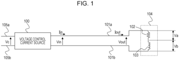
- Fig. 1 is a diagram illustrating an example of a voltage control current source 100 that drives a motor 104 in a wired connection state.
- the voltage control current source 100 outputs arbitrary current Iin that is first-order proportional to control voltage Vc input between control voltage input lines 105a and 105b.
- the motor 104 is capable of being represented by a series circuit composed of a resistor 102 and an inductor 103 as an equivalent circuit. The influence of parasitic capacitance occurring in the actual machine of the motor 104 is ignored for simplicity of description.
- the voltage control current source 100 is connected to the motor 104 via lead wires 101a and 101b.
- the voltage Vc is control voltage input between the control voltage input lines 105a and 105b.
- the current Iin is current output from the voltage control current source 100.
- Voltage Vin is voltage output from the voltage control current source 100.
- Voltage Va is voltage at both ends of the resistor 102.
- Voltage Vb is voltage at both ends of the inductor 103.
- Current Iout is current to flow into the motor 104.
- Voltage Vout is voltage at both ends of the motor 104.
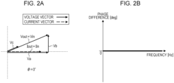
- Fig. 2A is a vector diagram indicating the phase relationship between the voltages Vc, Vin, Vout, Va, and Vb and the currents Iin and Iout.
- the upper direction of the vertical axis represents the orientation of phase lead and the lower direction of the vertical axis represents the orientation of phase lag.
- the voltage control current source 100 is connected to the motor 104 via the lead wires 101a and 101b. Accordingly, the current Iin output from the voltage control current source 100 is the same as the current Iout to flow into the motor 104. Consequently, the direction of the vector of the current Iin coincides with the direction of the vector of the current Iout, as illustrated in Fig. 2A . In other words, the phase difference between the current Iin and the current Iout is zero.
- the vector of the voltage Va with respect to the vector of the current Iout indicates a voltage drop occurring at the resistor 102
- the direction of the vector of the voltage Va coincides with the direction of the vector of the current Iout.
- the vector of the voltage Vb advances by 90 degrees with respect to the vector of the current Iout due to the influence of reactance of the inductor 103.
- the vector of the voltage Vout which is represented as combination of the vector of the voltage Va and the vector of the voltage Vb, advances with respect to the vector of the current Iout. In reverse representation of the reference of the voltage and the current, the vector of the current Iout is delayed with respect to the vector of the voltage Vout.
- Fig. 2B is a graph indicating the phase difference between the current Iin output from the voltage control current source 100 and the current Iout to flow into the motor 104 in a frequency domain. Since the current Iin output from the voltage control current source 100 is the same as the current Iout to flow into the motor 104, no phase difference occurs. Accordingly, as illustrated in Fig. 2B , the phase difference between the current Iin output from the voltage control current source 100 and the current Iout to flow into the motor 104 is zero at all frequencies.
- varying the amplitude or the phase of the control voltage Vc enables the current Iin output from the voltage control current source 100 to be varied to control the current Iout to flow into the motor 104.
- the phase difference between the current Iin output from the voltage control current source 100 and the current Iout to flow into the motor 104 is constantly zero (also viewed in the frequency domain).
- Fig. 3 is a diagram illustrating an example of the configuration of a wireless power transmission system 200 according to a first embodiment.
- the wireless power transmission system 200 includes a power transmitter 202, a power transmitter antenna 203, a power receiver antenna 204, and a power receiver 205.
- Lead wires 201a and 201b are paths through which power is supplied to the wireless power transmission system 200.
- Lead wires 206a and 206b are paths through which power output from the wireless power transmission system 200 is supplied to the motor.
- the power transmitter 202 switches the power supplied through the lead wires 201a and 201b and feeds the switched power to the power transmitter antenna 203.
- the power transmitter antenna 203 and the power receiver antenna 204 are arranged so as to be apart from each other by a distance achieving significant coupling with an electromagnetic field.
- the power receiver antenna 204 supplies part of electromagnetic field energy generated by the power transmitter antenna 203 to the power receiver 205.
- the power receiver 205 smooths the power supplied from the power receiver antenna 204.
- the power transmission efficiency of the wireless power transmission system 200 is not argued.
- the advantages of the first embodiment are produced regardless of the power transmission efficiency. It is assumed that the wireless power transmission system 200 performs a liner operation. In other words, the power supplied through the lead wires 201a and 201b has linear relationship with the power output through the lead wires 206a and 206b.
- Fig. 4 is a diagram illustrating an example of the specific configuration of the wireless power transmission system 200.
- the wireless power transmission system 200 receives positive or negative voltage from a positive and negative power supply 207 and supplies the positive or negative voltage to the motor 104.
- the motor 104 is an example of a load.
- the wireless power transmission system 200 includes the power transmitter 202, the power transmitter antenna 203, the power receiver antenna 204, the power receiver 205, a gate drive circuit 208, a matching circuit 209, a matching circuit 210, and a gate drive circuit 211.
- the power transmitter 202 includes four bi-directional switches 213.
- the sources of two field effect transistors (FETs) are connected to each other and the gates of the two FETs are connected to each other.
- the bi-directional switch 213 is driven with the same gate drive signal that operates based on source potential.
- the gate drive circuit 208 supplies the gate drive signal to each of the four bi-directional switches 213.
- the power receiver 205 includes four bi-directional switches 214.
- the sources of two field effect transistors (FETs) are connected to each other and the gates of the two FETs are connected to each other.
- the bi-directional switch 214 is driven with the same gate drive signal that operates based on the source potential.
- the gate drive circuit 211 supplies the gate drive signal to each of the four bi-directional switches 214.
- the positive and negative power supply 207 outputs positive or negative direct-current voltage.
- the amplitude of the voltage output from the positive and negative power supply 207 determines thrust of the motor 104.
- the positive or negative sign of the voltage output from the positive and negative power supply 207 determines the orientation in which the motor 104 moves.
- the gate drive circuit 208 supplies the gate drive signal of a predetermined frequency to the four bi-directional switches 213.
- the four bi-directional switches 213 switch the direct-current voltage output from the positive and negative power supply 207 in synchronization with the gate drive signal to convert the direct-current voltage output from the positive and negative power supply 207 into alternating-current voltage.
- the four bi-directional switches 213 apply the alternating-current voltage to the power transmitter antenna 203 via the matching circuit 209.
- the power transmitter antenna 203 generates the electromagnetic field energy and wirelessly transmits the power to the power receiver antenna 204.
- the matching circuit 209 is a capacitor and the power transmitter antenna 203 is a coil.
- the matching circuit 209 and the power transmitter antenna 203 serve as a resonant circuit that resonates at the same frequency as that of the bi-directional switches 213.
- the power receiver antenna 204 supplies part of the electromagnetic field energy generated by the power transmitter antenna 203 to the power receiver 205 via the matching circuit 210.
- the power receiver antenna 204 is a coil and the matching circuit 210 is a capacitor.
- the power receiver antenna 204 and the matching circuit 210 serve as a resonant circuit that resonates at the same frequency as that of the bi-directional switches 213.
- the power receiver 205 is a full-bridge synchronous rectifier using the bi-directional switches 214 that perform the switching at the same frequency as that of the bi-directional switches 213 and is adjusted so as to perform the switching in the phase producing the highest power reception efficiency.
- the power receiver 205 converts the alternating-current voltage supplied from the power receiver antenna 204 into the direct-current voltage and supplies the direct-current voltage to the motor 104.
- Fig. 5 is a graph indicating the relationship between the voltage input into the wireless power transmission system 200 in Fig. 4 and the voltage output from the wireless power transmission system 200 in Fig. 4 .
- the voltage input into the wireless power transmission system 200 is the same as the voltage output from the positive and negative power supply 207.
- the voltage input into the wireless power transmission system 200 is the same as the voltage input into the motor 104.
- the voltage input into the wireless power transmission system 200 and the voltage output from the wireless power transmission system 200 have positive first-order linear relationship. The input-output relationship illustrated in Fig.
- the wireless power transmission system 200 illustrated in Fig. 4 is capable of performing wireless power transmission of the negative voltage.
- a general wireless power transmission system that does not use the bi-directional switches 213 and 214 is not capable of performing the wireless power transmission of the negative voltage. This is because, upon input of the negative voltage, a body diode of the FET (or a parasitic element corresponding to the body diode) is made conductive and the FET is in a conductive state regardless of the state of the gate drive signal, thus causing an uncontrollable state.
- the wireless power transmission system 200 illustrated in Fig. 4 is capable of performing the wireless power transmission of the negative voltage, for example, it is possible to perform direct wireless power transmission of driving power of the motor 104.
- the current value to flow into the motor 104 is capable of being output from the voltage control current source 100 and the power output from the voltage control current source 100 is capable of being subjected to the wireless power transmission by the wireless power transmission system 200 illustrated in Fig. 4 .
- the positive and negative power supply 207 in Fig. 4 corresponds to the voltage control current source 100 in Fig. 1 .
- the control voltage corresponding to the current value to flow into the motor 104 is input into the voltage control current source 100 as the control voltage Vc.
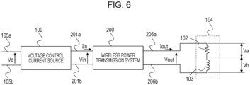
- Fig. 6 is a diagram illustrating a configuration in which the wireless power transmission system 200 in Fig. 4 performs the wireless power transmission of the power output from the voltage control current source 100 in Fig. 1 .
- the wireless power transmission system 200 in Fig. 4 is provided between the voltage control current source 100 and the motor 104 in the configuration in Fig. 6 , unlike the configuration in Fig. 1 .
- the wireless power transmission system 200 wirelessly transmits the power output from the voltage control current source 100 and supplies the power to the motor 104.
- the voltage control current source 100 is connected to the wireless power transmission system 200 via the lead wires 201a and 201b.
- the wireless power transmission system 200 is connected to the motor 104 via the lead wires 206a and 206b.
- the current Iin is current output from the voltage control current source 100.
- the voltage Vin is voltage input between the lead wires 201a and 201b.
- the voltage Vout is voltage between the lead wires 206a and 206b.
- the current Iout is current to flow into the motor 104.
- time delay corresponding to several tens of periods of a switching frequency of the power transmitter 202 may occur between the voltage Vin and the voltage Vout.
- the switching frequency of the power transmitter 202 is generally about several tens of times to about one thousand of times higher than a control frequency of the motor 104.
- the control frequency of the motor 104 is about 10 kHz while a frequency of 100 kHz to 15,000 kHz is selected as the switching frequency of the power transmitter 202.
- the delay between the voltage Vin and the voltage Vout which is caused by the wireless power transmission system 200 in Fig. 6 , is capable of being ignored in the first embodiment.
- the advantages of the first embodiment are not phenomena specifically produced with this precondition.
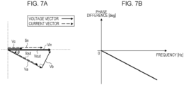
- Fig. 7A is a vector diagram indicating the phase relationship between the voltages Vc, Vin, Vout, Va, and Vb and the currents Iin and Iout in Fig. 6 .
- the upper direction of the vertical axis represents the orientation of the phase lead and the lower direction of the vertical axis represents the orientation of the phase lag.
- the phase of the control voltage Vc input into the voltage control current source 100 coincides with the phase of the current Iin output from the voltage control current source 100, as described above. Accordingly, the direction of the vector of the control voltage Vc coincides with the direction of the vector of the current Iin.
- Input impedance of the wireless power transmission system 200 is capable of being considered as actual resistance when viewed from an output terminal of the voltage control current source 100. This is because the switching frequency of the power transmitter 202 is generally about several tens of times to about one thousand of times higher than the control frequency of the motor 104 and a smoothing effect of a decoupling capacitor connected to a power supply input terminal of the wireless power transmission system 200 exists. Accordingly, little influence of the switching of the power transmitter 202 is exerted on the output terminal of the voltage control current source 100.
- the decoupling capacitor is constantly connected in a general designing method.
- the input impedance of the wireless power transmission system 200 is hereinafter considered as the actual resistance.
- the voltage input into the wireless power transmission system 200 (the voltage output from the voltage control current source 100) Vin is proportional to the current Iin output from the voltage control current source 100.
- the direction of the vector of the voltage Vin coincides with the direction of the vector of the current Iin.
- the wireless power transmission system 200 since the wireless power transmission system 200 immediately outputs the voltage Vin input between the lead wires 201a and 201b as the voltage Vout between the lead wires 206a and 206b, the direction of the vector of the voltage Vin coincides with the direction of the vector of the voltage Vout.
- the phase relationship between the vector of the voltage Vout and the vector of the current Iout is the same as the relationship described above with reference to Fig. 2A , a description of the phase relationship between the vector of the voltage Vout and the vector of the current Iout is omitted herein.
- the current Iout is delayed with respect to the vector of the voltage Vout ( ⁇ Vin). Since the direction of the vector of the voltage Vin coincides with the direction of the vector of the current Iin, the vector of the current Iout is delayed with respect to the vector of the current Iin.
- a phase difference ⁇ is the phase difference (an amount of lag) of the current Iout with respect to the current Iin.
- the phase difference ⁇ is represented by Expression (1).
- ⁇ denotes an angular frequency of the control voltage Vc
- L denotes the inductance of the inductor 103
- R denotes the resistance value of the resistor 102.
- Fig. 7B is a graph in which the phase difference is represented in the frequency domain.
- the phase difference between the current Iin output from the voltage control current source 100 and the current Iout to flow into the motor 104 is zero for all frequencies in Fig. 2B .
- the absolute value of the phase difference (the amount of lag) ⁇ is monotonically increased with the increasing frequency in Fig. 7B .
- the property in which the absolute value of the phase difference ⁇ is monotonically increased with the increasing frequency, as in Fig. 7B is not desirable.
- the phase difference between the current Iin output from the voltage control current source 100 and the current Iout to flow into the motor 104 is zero for all frequencies, as indicated in Fig. 2B .
- the timing (the phase) at which the motor 104 operates is delayed with respect to the control voltage Vc.
- the amount of lag is monotonically increased with the increasing frequency.
- the problem in the first embodiment is the difference that occurs between the phase of the current Iin input into the wireless power transmission system 200 and the phase of the current Iout output from the wireless power transmission system 200, which is caused by the electrical property of the wireless power transmission system 200.
- the phase compensator is adopted.
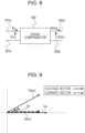
- Fig. 8 is a diagram illustrating the phase compensator 300 according to the first embodiment.
- Lead wires 301a and 301b are connected to an input portion of the phase compensator 300.
- Lead wires 302a and 302b are connected to an output portion of the phase compensator 300.
- the current Iin is current input into the phase compensator 300 through the lead wires 301a and 301b.
- the voltage Vin is voltage input between the lead wires 301a and 301b.
- Voltage V2out is voltage output between the lead wires 302a and 302b by the phase compensator 300.
- Current I2out is current output from the phase compensator 300 to the lead wires 302a and 302b.
- the phase compensator 300 is described to operate as an electric circuit.
- the phase compensator 300 may be installed as software using digital operations. Similarly, the phase compensator 300 may be installed as a logic circuit using a field programmable gate array (FPGA). Put another way, the phase compensator may be realized through a digital implementation or an analogue implementation or a combination of a digital and analogue.
- FPGA field programmable gate array
- Fig. 9 is a vector diagram for describing the advantages of phase compensation by the phase compensator 300 in Fig. 8 .
- the upper direction of the vertical axis represents the orientation of the phase lead.
- the lower direction of the vertical axis represents the orientation of the phase lag.
- the phase compensator 300 functions so as to advance the voltage V2out by an amount of phase compensation ⁇ with reference to the voltage Vin input between the lead wires 301a and 301b.
- the phase compensator 300 varies a power factor by the amount of phase compensation ⁇ .
- the vector of the voltage V2out output between the lead wires 302a and 302b is oriented to a direction that advances by the angle ⁇ with respect to the vector of the voltage Vin input between the lead wires 301a and 301b in Fig. 9 .
- the vector of the current I2out output from the phase compensator 300 is oriented to the same direction as that of the vector of the voltage Vin input between the lead wires 301a and 301b. How to resolve the above problem using the phase compensator 300 described above with reference to Fig. 8 and Fig. 9 will be described.
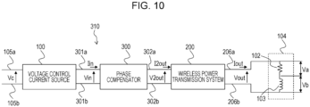
- Fig. 10 is a diagram illustrating an example of the configuration of a control apparatus 310 according to the first embodiment.
- the control apparatus 310 includes the voltage control current source 100, the phase compensator 300, the wireless power transmission system 200, and the motor 104. A method of controlling the control apparatus 310 will now be described.
- the voltage control current source 100 outputs arbitrary current Iin first-order proportional to the control voltage Vc input between the control voltage input lines 105a and 105b.
- the voltage control current source 100 is connected to the phase compensator 300 via the lead wires 301a and 301b.
- the current Iin is current output from the voltage control current source 100.
- the voltage Vin is voltage input between the lead wires 301a and 301b.
- the phase of the current Iin coincides with the phase of the voltage Vin, as indicated in Fig. 9 .
- the phase compensator 300 outputs the voltage V2out resulting from compensation of the phase of the voltage Vin.
- the voltage V2out is voltage the phase of which advances by the amount of phase compensation ⁇ with respect to the voltage Vin, as illustrated in Fig. 9 .
- the phase compensator 300 is connected to the wireless power transmission system 200 via the lead wires 302a and 302b.
- the voltage V2out is voltage output between the lead wires 302a and 302b by the phase compensator 300.
- the current I2out is current output from the phase compensator 300.
- the phase of the current I2out coincides with the phase of the current Iin, as indicated in Fig. 9 .
- the wireless power transmission system 200 receives the power of the voltage V2out, wirelessly transmits the power, and outputs the power of the voltage Vout.
- the wireless power transmission system 200 is connected to the motor 104 via the lead wires 206a and 206b.
- the voltage Vout is voltage output between the lead wires 206a and 206b by the wireless power transmission system 200.
- the current Iout is current output from the wireless power transmission system 200 to the motor 104.
- the motor 104 is capable of being represented by a series circuit composed of the resistor 102 and the inductor 103.
- the voltage Va is voltage at both ends of the resistor 102.
- the voltage Vb is voltage at both ends of the inductor 103.
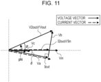
- Fig. 11 is a vector diagram indicating the phase relationship between the voltages Vc, Vin, V2out, Vout, Va, and Vb and the currents Iin, I2out and Iout in Fig. 10 .
- the upper direction of the vertical axis represents the orientation of the phase lead and the lower direction of the vertical axis represents the orientation of the phase lag.
- phase of the control voltage Vc input into the voltage control current source 100, the phase of the voltage Vin output from the voltage control current source 100, and the phase of the current Iin output from the voltage control current source 100 coincide with each other, as described above. Accordingly, the direction of the vector of the control voltage Vc, the direction of the vector of the voltage Vin, and the direction of the vector of the current Iin coincide with each other.
- the phase difference ⁇ in the phase lead direction occurs between the voltage Vin input into the phase compensator 300 and the voltage V2out output from the phase compensator 300. Accordingly, the vector of the voltage V2out is oriented to a direction that advances with respect to the vector of the voltage Vin by the angle ⁇ in Fig. 11 .
- phase of the current Iin input into the phase compensator 300 coincides with the phase of the current I2out output from the phase compensator 300, and the linear relationship is established between the phase of the current Iin input into the phase compensator 300 and the phase of the current I2out output from the phase compensator 300. Accordingly, the direction of the vector of the current Iin coincides with the direction of the vector of the current I2out.
- the linear relationship is established between the voltage V2out input into the wireless power transmission system 200 and the voltage Vout output from the wireless power transmission system 200.
- the direction of the vector of the voltage V2out coincides with the direction of the vector of the voltage Vout. Since the wireless power transmission system 200 immediately outputs the voltage V2out input between the lead wires 302a and 302b as the voltage Vout between the lead wires 206a and 206b, as described above, the direction of the vector of the voltage V2out coincides with the direction of the vector of the voltage Vout.
- the phase relationship between the voltages Vout, Va, and Vb and the current Iout is the same as the relationship described above with reference to Fig. 7A .
- the vector of the voltage Va with respect to the vector of the current Iout indicates a voltage drop occurring at the resistor 102
- the direction of the vector of the voltage Va coincides with the direction of the vector of the current Iout.
- the voltage Va has no lead and no lag with respect to the current Iout.
- the vector of the voltage Vb advances by 90 degrees with respect to the vector of the current Iout due to the influence of the reactance of the inductor 103.
- the vector of the voltage Vout which is represented as combination of the vector of the voltage Va and the vector of the voltage Vb, advances by the phase difference ⁇ with respect to the vector of the current Iout.
- the vector of the current Iout is delayed with respect to the vector of the voltage Vout by the phase difference ⁇ .
- the phase difference ⁇ is represented by Expression (1).
- the vector diagram when the relationship according to Expression (3) is established is indicated in Fig. 11 . [Formula 3] ⁇ ⁇ ⁇
- the amount of phase compensation ⁇ of the phase compensator 300 is adjusted so as to meet Expression (5). This minimizes the phase difference ⁇ between the control voltage Vc and the current Iout to flow into the motor 104 to suppress a delay of the timing (phase) at which the motor 104 operates with respect to the control voltage Vc.
- the problem of the first embodiment is the difference occurring between the phase of the control voltage Vc and the phase of the current Iout for driving the motor 104.
- the control apparatus 310 is capable of resolving the above problem by adopting the phase compensator 300 having the appropriate amount of phase compensation ⁇ so as to meet Expression (5).
- the voltage control current source 100 is an example of a linear motor driver 506 illustrated in Fig. 22A and Fig. 22B and outputs the power based on the control voltage Vc.
- the control voltage Vc is an example of a control signal.
- the wireless power transmission system 200 is connected downstream of the voltage control current source 100.
- the wireless power transmission system 200 receives first power and supplies second power to the motor 104 through the wireless power transmission.
- the phase compensator 300 is a compensator and compensates the difference between the phase of the control voltage Vc and the phase of the current Iout output from the wireless power transmission system 200.
- the phase of the current Iout output from the wireless power transmission system 200 is delayed with respect to the phase of the voltage Vout output from the wireless power transmission system 200.
- the phase compensator 300 is provided between the voltage control current source 100 and the wireless power transmission system 200.
- the phase compensator 300 receives the power output from the voltage control current source 100, and supplies the first power, in which the phase of the voltage V2out input into the wireless power transmission system 200 advances with respect to the phase of the voltage Vin output from the voltage control current source 100, to the wireless power transmission system 200.
- the wireless power transmission system 200 includes the power transmitter antenna 203, the power receiver antenna 204, the power transmitter 202, and the power receiver 205.
- the power transmitter antenna 203 is an antenna for the wireless power transmission.
- the power receiver antenna 204 wirelessly receives the power of the power transmitter antenna 203.
- the power transmitter 202 is a switch circuit.
- the power transmitter 202 switches the input power based on a first switching signal from the gate drive circuit 208 and applies the voltage to the power transmitter antenna 203.
- the power receiver 205 is a rectifier circuit.
- the power receiver 205 rectifies the voltage output from the power receiver antenna 204 based on a second switching signal from the gate drive circuit 211 and applies the rectified voltage to the motor 104.
- the power transmitter 202 includes the multiple bi-directional switches 213.
- the power receiver 205 includes the multiple bi-directional switches 214.
- the first switching signal has the same period as that of the second switching signal.
- the bi-directional switches 213 in the power transmitter 202 are driven with the first switching signal based on the potential of source terminals of the bi-directional switches 213.
- the bi-directional switches 214 in the power receiver 205 are driven with the second switching signal based on the potential of source terminals of the bi-directional switches 214.
- the control apparatus 310 drives the motor 104 with the current Iout output from the wireless power transmission system 200.
- the phase compensator 300 compensates the difference occurring between the phase of the control voltage Vc input into the control apparatus 310 and the phase of the current Iout for driving the motor 104, which is output from the wireless power transmission system 200, due to the electrical property of the wireless power transmission system 200. Reducing the difference by the phase compensator 300 enables a control speed and a control accuracy of the motor 104 to be improved.
- Fig. 12 is a diagram illustrating an example of the configuration of a control apparatus 410 according to a second embodiment.
- the control apparatus 410 includes a phase compensator 400, the voltage control current source 100, the wireless power transmission system 200, and the motor 104.
- the phase compensator 400 is provided upstream of the voltage control current source 100 and has the same function as that of the phase compensator 300 of the first embodiment.
- Lead wires 401a and 401b are connected to an input portion of the phase compensator 400.
- the phase compensator 400 is connected to the voltage control current source 100 via lead wires 402a and 402b.
- the phase compensator 400 receives control voltage Vc1 between the lead wires 401a and 401b, performs the phase compensation of the amount of phase compensation ⁇ , and outputs control voltage Vc2 between the lead wires 402a and 402b.
- the control voltage Vc2 is voltage resulting from advancing the phase of the control voltage Vc1 by the amount of phase compensation ⁇ .
- the voltage control current source 100 outputs arbitrary current Iin first-order proportional to the control voltage Vc2 input between the lead wires 402a and 402b.
- the voltage control current source 100 is connected to the wireless power transmission system 200 via the lead wires 201a and 201b.
- the current Iin is current output from the voltage control current source 100.
- the voltage Vin is voltage output between the lead wires 201a and 201b by the voltage control current source 100.
- the wireless power transmission system 200 receives the power of the voltage Vin, wirelessly transmits the power, and outputs the power of the voltage Vout.
- the wireless power transmission system 200 is connected to the motor 104 via the lead wires 206a and 206b.
- the voltage Vout is voltage output between the lead wires 206a and 206b by the wireless power transmission system 200.
- the current Iout is current output from the wireless power transmission system 200 to the motor 104.
- the motor 104 is capable of being represented by a series circuit composed of the resistor 102 and the inductor 103.
- the voltage Va is voltage at both ends of the resistor 102.
- the voltage Vb is voltage at both ends of the inductor 103.
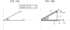
- Fig. 13A is a vector diagram for describing the advantages of phase compensation by the phase compensator 400.
- the phase compensator 400 functions so as to advance the control voltage Vc2 by the amount of phase compensation ⁇ with reference to the control voltage Vc1. Accordingly, the vector of the control voltage Vc2 is oriented to a direction the phase of which advances by the amount of phase compensation ⁇ with respect to the vector of the control voltage Vc1.
- the amount of phase compensation ⁇ meets Expression (5) described above.
- Fig. 13B is a vector diagram indicating the phase relationship between the voltages Vc1, Vc2, Vin, Vout, Va, and Vb and the currents Iin and Iout.
- the upper direction of the vertical axis represents the orientation of the phase lead and the lower direction of the vertical axis represents the orientation of the phase lag.
- the phase difference of the amount of phase compensation ⁇ exists between the control voltage Vc1 and the control voltage Vc2. Accordingly, the vector of the control voltage Vc2 is oriented to a direction the phase of which advances by the amount of phase compensation ⁇ with respect to the vector of the control voltage Vc1.
- phase of the control voltage Vc2 input into the voltage control current source 100, the phase of the voltage Vin output from the voltage control current source 100, and the phase of the current Iin output from the voltage control current source 100 coincide with each other, as described above. Accordingly, the direction of the vector of the control voltage Vc2, the direction of the vector of the voltage Vin, and the direction of the vector of the current Iin coincide with each other.
- the linear relationship is established between the voltage Vin input into the wireless power transmission system 200 and the voltage Vout output from the wireless power transmission system 200.
- the direction of the vector of the voltage Vin coincides with the direction of the vector of the voltage Vout. Since the wireless power transmission system 200 immediately outputs the voltage Vin input between the lead wires 201a and 201b as the voltage Vout between the lead wires 206a and 206b, as assumed above, the direction of the vector of the voltage Vin coincides with the direction of the vector of the voltage Vout.
- the phase relationship between the voltages Vout, Va, and Vb and the current Iout is the same as the relationship described above with reference to Fig. 7A .
- the vector of the voltage Va with respect to the vector of the current Iout indicates a voltage drop occurring at the resistor 102
- the direction of the vector of the voltage Va coincides with the direction of the vector of the current Iout.
- the voltage Va has no lead and no lag with respect to the current Iout.
- the vector of the voltage Vb advances by 90 degrees with respect to the vector of the current Iout due to the influence of the reactance of the inductor 103.
- the vector of the voltage Vout which is represented as combination of the vector of the voltage Va and the vector of the voltage Vb, advances by the phase difference ⁇ with respect to the vector of the current Iout.
- the vector of the current Iout is delayed with respect to the vector of the voltage Vout by the phase difference ⁇ .
- the phase difference ⁇ is represented by Expression (1) indicated above. Since the amount of phase compensation ⁇ meets Expression (5) described above, the phase difference occurring between the control voltage Vc1 and the current Iout to flow into the motor 104 is approximately zero.
- the control apparatus 410 has the advantage of reducing the phase difference between the phase of the control voltage Vc 1 and the phase of the current Iout for driving the motor 104, as in the first embodiment.
- Two configuration examples will now be described as specific examples of the configuration of the phase compensator 400.
- Fig. 14 is a diagram illustrating an example of the configuration of the phase compensator 400 composed of an analog circuit using an operational amplifier U1.
- the phase compensator 400 includes the operational amplifier U1, resistors R1 to R4, and capacitors C1 and C2 and has a configuration based on a non-inverting amplifier circuit.
- the resistor R1 has a resistance of 300 ⁇
- the resistor R2 has a resistance of 10 kQ
- the resistor R3 has a resistance of 400 ⁇
- the resistor R4 has a resistance of 1.2 kQ.
- the capacitor C1 has a capacitance of 0.2 ⁇ F and the capacitor C2 has a capacitance of 0.3 ⁇ F.
- the phase compensator 400 receives the control voltage Vc1 based on ground potential and gains the control voltage Vc2 based on the ground potential.
- Fig. 15A and Fig. 15B are graphs indicating transmission characteristics of the phase compensator 400 in Fig. 14 .
- the horizontal axis represents frequency and the vertical axis represents the ratio in amplitude (power) of the control voltage Vc2 to the control voltage Vc1 in units of dB.
- the horizontal axis represents frequency and the vertical axis represents the phase difference between the control voltage Vc1 and the control voltage Vc2 in units of degrees.
- the application of the wireless power transmission system 200 has no small influence on the amplitude relationship. Accordingly, varying the amplitude relationship between the control voltage Vc1 and the current Iout to flow into the motor 104 at each frequency with the phase compensator 300 or the phase compensator 400, like the amplitude characteristic illustrated in Fig. 15A , is not denied in the second embodiment.
- the use of the phase compensator 300 or the phase compensator 400 enables the improvement effect of the control apparatus 310 or 410 to which the wireless power transmission system 200 is applied to be enforced.
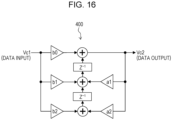
- Fig. 16 is a diagram illustrating an example of the configuration of the phase compensator 400 using an infinite impulse response (IIR) digital filter.
- the phase compensator 400 receives the control voltage Vc1 and outputs the control voltage Vc2.
- This digital filter may be installed as software using digital operations. Similarly, this digital filter may be installed as a logic circuit using the FPGA.
- the values of the weighting coefficients a1, a2, b0, b1, and b2 are derived through Z conversion using bilinear transform for the phase compensator 400 composed of the analog circuit using the operational amplifier U1 illustrated in Fig. 14 . Accordingly, when the values of the weighting coefficients a1, a2, b0, b 1, and b2 are used in the IIR digital filter illustrated in Fig. 16 , the transmission characteristics of the IIR digital filter illustrated in Fig. 16 are substantially equivalent to those in Fig. 15A and Fig. 15B .
- phase compensator 400 The two specific configuration examples of the phase compensator 400 are described above. As apparent from these examples, the phase compensator 300 and the phase compensator 400 adopted in the first embodiment and the second embodiment, respectively, are capable of being practically realized and installed. Results of measurement of the advantages of the phase compensator 300 and the phase compensator 400 in the actual machine of the control apparatus to which the wireless power transmission system 200 is applied will be described in a third embodiment.
- the voltage control current source 100 outputs the power based on the control voltages Vc1 and Vc2.
- Each of the control voltages Vc1 and Vc2 is an example of the control signal.
- the wireless power transmission system 200 is connected downstream of the voltage control current source 100.
- the wireless power transmission system 200 receives the first power and supplies the second power to the motor 104 through the wireless power transmission.
- the phase compensator 400 is a compensator and compensates the difference between the phase of the control voltage Vc1 and the phase of the current Iout output from the wireless power transmission system 200.
- the phase of the current Iout output from the wireless power transmission system 200 is delayed with respect to the phase of the voltage Vout output from the wireless power transmission system 200, as illustrated in Fig. 13B .
- the voltage control current source 100 receives the control voltage Vc2.
- the phase compensator 400 is provided upstream of the voltage control current source 100.
- the phase compensator 400 receives the control voltage Vc1 and supplies the control voltage Vc2 the phase of which advances with respect to the phase of the control voltage Vc 1 to the voltage control current source 100.
- the phase compensator 400 may compensate the difference between the phase of the control voltage Vc 1 and the phase of the current Iout output from the wireless power transmission system 200 and the difference between the amplitude of the control voltage Vc 1 and the amplitude of the current Iout output from the wireless power transmission system 200.
- phase compensator 300 in Fig. 10 may compensate the difference between the phase of the control voltage Vc and the phase of the current Iout output from the wireless power transmission system 200 and the difference between the amplitude of the control voltage Vc and the amplitude of the current Iout output from the wireless power transmission system 200.
- the phase compensators 300 and 400 may be composed of the analog circuits, such as the one illustrated in Fig. 14 .
- the phase compensators 300 and 400 may compensate the difference in phase using the digital operations illustrated in Fig. 16 .
- the digital operations include both arithmetic processing of programs by a digital signal processor (DSP) or a personal computer and parallel arithmetic processing by a digital circuit using the FPGA.
- DSP digital signal processor
- the transmission characteristics of the phase compensators 300 and 400 are transmission characteristics that offset the phase difference between the current input into the wireless power transmission system 200 and the current output from the wireless power transmission system 200.
- the transmission characteristics of the phase compensators 300 and 400 may be transmission characteristics that offset the phase difference between the voltage input into the wireless power transmission system 200 and the current output from the wireless power transmission system 200.
- the control apparatus 410 drives the motor 104 with the current Iout output from the wireless power transmission system 200.
- the phase compensator 400 compensates the difference occurring between the phase of the control voltage Vc 1 input into the control apparatus 410 and the phase of the current Iout for driving the motor 104, which is output from the wireless power transmission system 200, due to the electrical property of the wireless power transmission system 200. Reducing the difference by the phase compensator 400 enables the control speed and the control accuracy of the motor 104 to be improved.
- phase compensator 300 or 400 in a positioning stage having the wireless power transmission system 200 installed thereon will now be described.
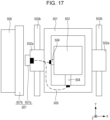
- Fig. 17 is a top view illustrating an example of the configuration of the positioning stage using a wireless power transmission system 507 for power supply to a linear motor.
- a stage on which reticle of a semiconductor exposure apparatus is installed is exemplified in the third embodiment.
- the positioning stage in the third embodiment includes a coarse-motion stage 501 having a large stroke and a fine-motion stage 503 having a high positioning accuracy.
- a pair of needles 502a are provided at left and right sides of the driving direction (the Y-axis direction) of the coarse-motion stage 501.
- the pair of needles 502a are driven in the Y-axis direction in cooperation with the corresponding pair of stators 502b.
- a reflecting mirror (not illustrated) is provided on the coarse-motion stage 501. Measured light from a laser interferometer (a measurer) (not illustrated) is reflected by the reflecting mirror to measure the amount of displacement or the position to the Y-axis direction of the stage.
- the fine-motion stage 503 is connected to the coarse-motion stage 501 with a fine-motion linear motor 504 in a non-contact manner to be driven in the Y-axis direction with the coarse-motion stage 501.
- the fine-motion stage 503 is connected to the coarse-motion stage 501 also in the X-axis direction with the fine-motion linear motor 504 in a non-contact manner to be driven in the X-axis direction.
- a reflecting mirror (not illustrated) is provided on the fine-motion stage 503. Measured light from a laser interferometer (a measurer) (not illustrated) is reflected by the reflecting mirror to measure the amounts of displacement or the positions to the X-axis direction and the Y-axis direction of the stage.
- the power to drive the fine-motion linear motor 504 is supplied from the linear motor driver 506.
- the power supplied from the linear motor driver 506 is transmitted to the fine-motion linear motor 504 via a power transmitter 507b and a power receiver 507a of the wireless power transmission system 507 and fine-motion linear motor cables 505.
- the power transmitter 507b of the wireless power transmission system 507 detects current output from the linear motor driver 506 and transmits the power to the power receiver 507a via the power transmitter antenna.
- the power receiver 507a receives the power transmitted from the power transmitter 507b via the power receiver antenna and supplies the power to the fine-motion linear motor 504 via the rectifier circuit.
- FIG. 18 is a diagram illustrating an example of the configuration of the control apparatus 600 when the phase compensator is not provided.
- the control apparatus 600 includes a subtracter 605, a compensator 604, the linear motor driver 506, the wireless power transmission system 507, the fine-motion linear motor 504, the fine-motion stage 503, and a position measurer 603.
- the linear motor driver 506 corresponds to the voltage control current source 100 in Fig. 10 or Fig. 12 .
- the wireless power transmission system 507 corresponds to the wireless power transmission system 200 in Fig. 10 or Fig. 12 .
- the fine-motion linear motor 504 corresponds to the motor 104 in Fig. 10 or Fig. 12 .
- the position of the fine-motion stage 503 is measured by the position measurer 603, such as a laser interferometer, and the measured position of the fine-motion stage 503 is supplied to the subtracter 605.
- the subtracter 605 supplies the difference (deviation) between the position of the fine-motion stage 503, which is measured by the position measurer 603, and a position instruction value (a target position) to the compensator 604.
- the compensator 604 includes, for example, a proportional-integral-derivative (PID) controller 601.
- PID proportional-integral-derivative
- the compensator 604 generates a driver instruction value for the linear motor driver 506 based on the deviation supplied from the subtracter 605.
- the linear motor driver 506 outputs the motor drive current based on the driver instruction value from the compensator 604.
- the motor drive current output from the linear motor driver 506 is received by the wireless power transmission system 507 and is supplied to the fine-motion linear motor 504 via a wireless antenna and the rectifier circuit.
- the fine-motion linear motor 504 applies the thrust to the fine-motion stage 503 in accordance with the supplied motor drive current.
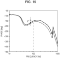
- Fig. 19 is a graph indicating closed loop phase characteristics of the position feedback control system in the X-axis direction of the fine-motion stage 503 when the power transmission is performed using the wireless power transmission system 507 and when the power transmission is performed using a wired manner (for example, using cables).
- a solid line indicates the closed loop phase characteristic in the power transmission in the wired manner
- a broke line indicates the closed loop phase characteristic in the power transmission using the wireless power transmission system 507.
- Comparison between the phase characteristic in the wired manner indicated by the solid line and the phase characteristic in the wireless power transmission indicated by the broken line indicates that the response of the wireless power transmission indicated by the broken line is delayed with respect to the response of the wired manner indicated by the solid line by 9 degrees, for example, when sinewaves of 100 Hz are input.
- the fine-motion stage 503 was driven in the X-axis direction from a stage position P0 to a stage position P1 in a manner illustrated in Fig. 20 in the state in which the phase of the wireless power transmission indicated by the broken line is delayed with respect to the phase of the wired manner indicated by the solid line.
- Fig. 21 indicates the stage deviation at that time. Referring to Fig.
- a solid line indicates the stage deviation in the wired manner and a broken line indicates the stage deviation in the wireless power transmission. Since the response in the wireless power transmission indicated by the broken line is delayed with respect to the response in the wired manner indicated by the solid line, the control performance of the fine-motion stage 503 was degraded and the large stage deviation occurred.
- Fig. 22A is a diagram illustrating an example of the configuration of a control apparatus 610 including a phase compensator 602.
- the control apparatus 610 in Fig. 22A results from addition of the phase compensator 602 to the control apparatus 600 in Fig. 18 .
- the phase compensator 602 is provided between the PID controller 601 and the linear motor driver 506.
- the phase compensator 602 receives the value output from the PID controller 601, performs the phase compensation, and supplies the driver instruction value to the linear motor driver 506.
- the phase compensator 602 corresponds to the phase compensator 400 in Fig. 12 .
- Coefficients a1, a2, b0, b1, and b2 in Expression (7) correspond to the weighting coefficients a1, a2, b0, b1, and b2 in Fig. 16 .
- Expression (7) is an equation when the phase compensator 602 is installed as the digital circuit, the phase compensator 602 may be installed as the analog circuit.
- the weighting coefficients a1, a2, b0, b1, and b2 of the phase compensator 602 are adjusted so as to compensate the difference in the phase characteristic between the power transmission using the wireless power transmission system 507 and the power transmission in the wired manner.
- the phase compensator 602 having the characteristic in Fig. 23 is capable of being installed by using these weighting coefficients.
- Fig. 22B is a diagram illustrating an example of the configuration of another control apparatus 620 including the phase compensator 602.
- the control apparatus 620 in Fig. 22B results from addition of the phase compensator 602 to the control apparatus 600 in Fig. 18 .
- the phase compensator 602 is provided between the linear motor driver 506 and the wireless power transmission system 507.
- the phase compensator 602 receives the motor drive current output from the linear motor driver 506, performs the phase compensation, and supplies the motor drive current to the wireless power transmission system 507.
- the phase compensator 602 corresponds to the phase compensator 300 in Fig. 10 .
- Fig. 24 is a graph indicating the closed loop phase characteristics of the position feedback control system in the X-axis direction of the fine-motion stage 503 when the power transmission is performed using the wireless power transmission system 507 with phase compensator 602 in Fig. 22B and when the power transmission is performed using the wired manner.
- a solid line indicates the closed loop phase characteristic in the power transmission in the wired manner
- a broke line indicates the closed loop phase characteristic in the power transmission using the wireless power transmission system 507.
- Comparison between the phase characteristic in the wired manner indicated by the solid line and the phase characteristic in the wireless power transmission indicated by the broken line indicates that the response of the wireless power transmission indicated by the broken line is delayed with respect to the response of the wired manner indicated by the solid line by 0.1 degrees, that is, little delay occurs, for example, when sinewaves of 100 Hz are input.
- the fine-motion stage 503 was driven in the same manner as in Fig. 20 in the state in which the closed loop phase characteristic in the wired manner indicated by the solid line substantially coincides with the closed loop phase characteristic in the wireless power transmission indicated by the broken line.
- Fig. 25 indicates the stage deviation at that time. Referring to Fig.
- a solid line indicates the stage deviation in the wired manner and a broken line indicates the stage deviation in the wireless power transmission. Since the phase characteristic of the fine-motion stage 503 in the wireless power transmission indicated by the broken line was equivalent to the phase characteristic of the fine-motion stage 503 in the wired manner indicated by the solid line, the control performance of the fine-motion stage 503 in the wireless power transmission was equivalent to that in the wired manner. As a result, the stage deviation in the wireless power transmission was equivalent to the stage deviation in the wired manner.
- the fine-motion linear motor 504 corresponds to the motor 104 of the first and second embodiments and applies the thrust to the fine-motion stage 503, which is driven with an object being held.
- the fine-motion stage 503 is a stage apparatus.
- At least one fine-motion linear motor 504 may be configured on the fine-motion stage 503.
- the wireless power transmission system 507 is connected to each fine-motion linear motor 504.
- the wireless power transmission system 507 transmits the power to at least one fine-motion linear motor 504.
- Embodiments of the present invention can also be realized by a computer of a system or apparatus that reads out and executes computer executable instructions (e.g., one or more programs) recorded on a storage medium (which may also be referred to more fully as a 'non-transitory computer-readable storage medium') to perform the functions of one or more of the above-described embodiments and/or that includes one or more circuits (e.g., application specific integrated circuit (ASIC)) for performing the functions of one or more of the above-described embodiments, and by a method performed by the computer of the system or apparatus by, for example, reading out and executing the computer executable instructions from the storage medium to perform the functions of one or more of the above-described embodiments and/or controlling the one or more circuits to perform the functions of one or more of the above-described embodiments.
- ASIC application specific integrated circuit
- the computer may comprise one or more processors (e.g., central processing unit (CPU), micro processing unit (MPU)) and may include a network of separate computers or separate processors to read out and execute the computer executable instructions.
- the computer executable instructions may be provided to the computer, for example, from a network or the storage medium.
- the storage medium may include, for example, one or more of a hard disk, a random-access memory (RAM), a read only memory (ROM), a storage of distributed computing systems, an optical disk (such as a compact disc (CD), digital versatile disc (DVD), or Blu-ray Disc (BD) TM ), a flash memory device, a memory card, and the like.
Landscapes
- Engineering & Computer Science (AREA)
- Power Engineering (AREA)
- Computer Networks & Wireless Communication (AREA)
- Control Of Ac Motors In General (AREA)
- Exposure And Positioning Against Photoresist Photosensitive Materials (AREA)
- Control Of Linear Motors (AREA)
- Electric Propulsion And Braking For Vehicles (AREA)
Abstract
Description
- The disclosure relates to a control apparatus and a method of controlling the control apparatus.
- Systems have been proposed in which power is supplied to a linear motor to drive the liner motor. For example, in a semiconductor exposure apparatus, a motor that fine-moves reticle is installed on a reticle stage for moving the reticle to the exposure apparatus. A power supply cable for supplying the power to drive the motor is connected on the stage. Since the power supply cable moves with the movement of the stage, the tension of the cable influences the accuracy of positioning of the stage and the time required to complete the positioning. Accordingly, wireless transmission of the power for driving the motor is considered in order to improve the performance of the semiconductor exposure apparatus.
-
Japanese Patent Laid-Open No. 2018-54847 Japanese Patent Laid-Open No. 2018-54847 - The present invention in its first aspect provides a control apparatus as specified in
claim 1. Preferably or optional features are specified inclaims 2 to 15. - The present invention in its second aspect provides a method of controlling the control apparatus as specified in
claim 16. - Further features of the present invention will become apparent from the following description of embodiments with reference to the attached drawings.
-
-
Fig. 1 is a diagram illustrating an example of a voltage control current source that drives a motor in a wired connection state. -
Fig. 2A and Fig. 2B illustrate the phase relationship between output current and flowing-into current. -
Fig. 3 is a diagram illustrating an example of the configuration of a wireless power transmission system. -
Fig. 4 is a diagram illustrating an example of the specific configuration of the wireless power transmission system. -
Fig. 5 is a graph indicating the relationship between voltage input into the wireless power transmission system and voltage output from the wireless power transmission system. -
Fig. 6 is a diagram illustrating a configuration in which power output from the voltage control current source is subjected to wireless power transmission. -
Fig. 7A and Fig. 7B illustrate the phase relationship between the output current and the flowing-into current. -
Fig. 8 is a diagram illustrating a phase compensator. -
Fig. 9 is a vector diagram for describing the advantages of phase compensation by the compensator. -
Fig. 10 is a diagram illustrating a configuration in which the phase compensator is connected in a control apparatus. -
Fig. 11 is a vector diagram indicating the phase relationship between voltages and currents. -
Fig. 12 is a diagram illustrating an example of the configuration of a control apparatus including a phase compensator. -
Fig. 13A and Fig. 13B are vector diagrams for describing the advantages of phase compensation by the phase compensator. -
Fig. 14 is a diagram illustrating an example of the configuration of the phase compensator composed of an analog circuit. -
Fig. 15A and Fig. 15B are graphs indicating transmission characteristics of the phase compensator. -
Fig. 16 is a diagram illustrating an example of the configuration of the phase compensator using a digital filter. -
Fig. 17 is a top view illustrating an example of the configuration of a positioning stage. -
Fig. 18 is a diagram illustrating an example of the configuration of a control apparatus. -
Fig. 19 is a graph indicating closed loop phase characteristics of a position feedback control system. -
Fig. 20 is a graph indicating stage positions when a fine-motion stage is driven in the X-axis direction. -
Fig. 21 is a graph indicating stage deviation when the fine-motion stage is driven. -
Fig. 22A and Fig. 22B are diagrams illustrating examples of the configurations of control apparatuses each including a phase compensator. -
Fig. 23 is a graph indicating a phase characteristic of the phase compensator for compensating delay in the phase characteristic. -
Fig. 24 is a graph indicating the closed loop phase characteristics of the position feedback control system. -
Fig. 25 is a graph indicating the stage deviation when the fine-motion stage is driven. -
Fig. 1 is a diagram illustrating an example of a voltage controlcurrent source 100 that drives amotor 104 in a wired connection state. The voltage controlcurrent source 100 outputs arbitrary current Iin that is first-order proportional to control voltage Vc input between controlvoltage input lines motor 104 is capable of being represented by a series circuit composed of aresistor 102 and aninductor 103 as an equivalent circuit. The influence of parasitic capacitance occurring in the actual machine of themotor 104 is ignored for simplicity of description. The voltage controlcurrent source 100 is connected to themotor 104 vialead wires - The voltage Vc is control voltage input between the control
voltage input lines - The current Iin is current output from the voltage control
current source 100. Voltage Vin is voltage output from the voltage controlcurrent source 100. Voltage Va is voltage at both ends of theresistor 102. Voltage Vb is voltage at both ends of theinductor 103. Current Iout is current to flow into themotor 104. - Voltage Vout is voltage at both ends of the
motor 104. -
Fig. 2A is a vector diagram indicating the phase relationship between the voltages Vc, Vin, Vout, Va, and Vb and the currents Iin and Iout. Referring toFig. 2A , the upper direction of the vertical axis represents the orientation of phase lead and the lower direction of the vertical axis represents the orientation of phase lag. - In the configuration illustrated in
Fig. 1 , the voltage controlcurrent source 100 is connected to themotor 104 via thelead wires current source 100 is the same as the current Iout to flow into themotor 104. Consequently, the direction of the vector of the current Iin coincides with the direction of the vector of the current Iout, as illustrated inFig. 2A . In other words, the phase difference between the current Iin and the current Iout is zero. - Attention is given to the phase difference in voltage between the respective components here. Since the vector of the voltage Va with respect to the vector of the current Iout indicates a voltage drop occurring at the
resistor 102, the direction of the vector of the voltage Va coincides with the direction of the vector of the current Iout. In other words, the voltage Va has no lead and no lag with respect to the current Iout. In contrast, the vector of the voltage Vb advances by 90 degrees with respect to the vector of the current Iout due to the influence of reactance of theinductor 103. The vector of the voltage Vout, which is represented as combination of the vector of the voltage Va and the vector of the voltage Vb, advances with respect to the vector of the current Iout. In reverse representation of the reference of the voltage and the current, the vector of the current Iout is delayed with respect to the vector of the voltage Vout. -
Fig. 2B is a graph indicating the phase difference between the current Iin output from the voltage controlcurrent source 100 and the current Iout to flow into themotor 104 in a frequency domain. Since the current Iin output from the voltage controlcurrent source 100 is the same as the current Iout to flow into themotor 104, no phase difference occurs. Accordingly, as illustrated inFig. 2B , the phase difference between the current Iin output from the voltage controlcurrent source 100 and the current Iout to flow into themotor 104 is zero at all frequencies. - Consequently, in the configuration illustrated in
Fig. 1 , varying the amplitude or the phase of the control voltage Vc enables the current Iin output from the voltage controlcurrent source 100 to be varied to control the current Iout to flow into themotor 104. At this time, the phase difference between the current Iin output from the voltage controlcurrent source 100 and the current Iout to flow into themotor 104 is constantly zero (also viewed in the frequency domain). A control apparatus that drives the motor with current output from a wireless power transmission system will now be described. -
Fig. 3 is a diagram illustrating an example of the configuration of a wirelesspower transmission system 200 according to a first embodiment. - The wireless
power transmission system 200 includes apower transmitter 202, apower transmitter antenna 203, apower receiver antenna 204, and apower receiver 205.Lead wires power transmission system 200.Lead wires power transmission system 200 is supplied to the motor. Thepower transmitter 202 switches the power supplied through thelead wires power transmitter antenna 203. Thepower transmitter antenna 203 and thepower receiver antenna 204 are arranged so as to be apart from each other by a distance achieving significant coupling with an electromagnetic field. Thepower receiver antenna 204 supplies part of electromagnetic field energy generated by thepower transmitter antenna 203 to thepower receiver 205. Thepower receiver 205 smooths the power supplied from thepower receiver antenna 204. In the description of the first embodiment, the power transmission efficiency of the wirelesspower transmission system 200 is not argued. The advantages of the first embodiment are produced regardless of the power transmission efficiency. It is assumed that the wirelesspower transmission system 200 performs a liner operation. In other words, the power supplied through thelead wires lead wires -
Fig. 4 is a diagram illustrating an example of the specific configuration of the wirelesspower transmission system 200. The wirelesspower transmission system 200 receives positive or negative voltage from a positive andnegative power supply 207 and supplies the positive or negative voltage to themotor 104. Themotor 104 is an example of a load. The wirelesspower transmission system 200 includes thepower transmitter 202, thepower transmitter antenna 203, thepower receiver antenna 204, thepower receiver 205, agate drive circuit 208, amatching circuit 209, amatching circuit 210, and agate drive circuit 211. - The
power transmitter 202 includes fourbi-directional switches 213. In each of thebi-directional switches 213, the sources of two field effect transistors (FETs) are connected to each other and the gates of the two FETs are connected to each other. Thebi-directional switch 213 is driven with the same gate drive signal that operates based on source potential. Thegate drive circuit 208 supplies the gate drive signal to each of the fourbi-directional switches 213. - The
power receiver 205 includes fourbi-directional switches 214. In each of thebi-directional switches 214, the sources of two field effect transistors (FETs) are connected to each other and the gates of the two FETs are connected to each other. Thebi-directional switch 214 is driven with the same gate drive signal that operates based on the source potential. Thegate drive circuit 211 supplies the gate drive signal to each of the fourbi-directional switches 214. - The positive and
negative power supply 207 outputs positive or negative direct-current voltage. The amplitude of the voltage output from the positive andnegative power supply 207 determines thrust of themotor 104. The positive or negative sign of the voltage output from the positive andnegative power supply 207 determines the orientation in which themotor 104 moves. - The
gate drive circuit 208 supplies the gate drive signal of a predetermined frequency to the fourbi-directional switches 213. The fourbi-directional switches 213 switch the direct-current voltage output from the positive andnegative power supply 207 in synchronization with the gate drive signal to convert the direct-current voltage output from the positive andnegative power supply 207 into alternating-current voltage. The fourbi-directional switches 213 apply the alternating-current voltage to thepower transmitter antenna 203 via thematching circuit 209. Thepower transmitter antenna 203 generates the electromagnetic field energy and wirelessly transmits the power to thepower receiver antenna 204. For example, thematching circuit 209 is a capacitor and thepower transmitter antenna 203 is a coil. Thematching circuit 209 and thepower transmitter antenna 203 serve as a resonant circuit that resonates at the same frequency as that of the bi-directional switches 213. - The
power receiver antenna 204 supplies part of the electromagnetic field energy generated by thepower transmitter antenna 203 to thepower receiver 205 via thematching circuit 210. For example, thepower receiver antenna 204 is a coil and thematching circuit 210 is a capacitor. Thepower receiver antenna 204 and thematching circuit 210 serve as a resonant circuit that resonates at the same frequency as that of the bi-directional switches 213. - The
power receiver 205 is a full-bridge synchronous rectifier using thebi-directional switches 214 that perform the switching at the same frequency as that of thebi-directional switches 213 and is adjusted so as to perform the switching in the phase producing the highest power reception efficiency. Thepower receiver 205 converts the alternating-current voltage supplied from thepower receiver antenna 204 into the direct-current voltage and supplies the direct-current voltage to themotor 104. -
Fig. 5 is a graph indicating the relationship between the voltage input into the wirelesspower transmission system 200 inFig. 4 and the voltage output from the wirelesspower transmission system 200 inFig. 4 . The voltage input into the wirelesspower transmission system 200 is the same as the voltage output from the positive andnegative power supply 207. The voltage input into the wirelesspower transmission system 200 is the same as the voltage input into themotor 104. The voltage input into the wirelesspower transmission system 200 and the voltage output from the wirelesspower transmission system 200 have positive first-order linear relationship. The input-output relationship illustrated inFig. 5 is established in a case in which the gate drive signals output from thegate drive circuit 208 and thegate drive circuit 211 are in a synchronized state and the phase difference between the gate drive signals output from thegate drive circuit 208 and thegate drive circuit 211 is appropriately adjusted. - The wireless
power transmission system 200 illustrated inFig. 4 is capable of performing wireless power transmission of the negative voltage. A general wireless power transmission system that does not use thebi-directional switches - Since the wireless
power transmission system 200 illustrated inFig. 4 is capable of performing the wireless power transmission of the negative voltage, for example, it is possible to perform direct wireless power transmission of driving power of themotor 104. Specifically, in a normal rotation operation and a reverse rotation operation of themotor 104 inFig. 1 , the current value to flow into themotor 104 is capable of being output from the voltage controlcurrent source 100 and the power output from the voltage controlcurrent source 100 is capable of being subjected to the wireless power transmission by the wirelesspower transmission system 200 illustrated inFig. 4 . In other words, the positive andnegative power supply 207 inFig. 4 corresponds to the voltage controlcurrent source 100 inFig. 1 . At this time, the control voltage corresponding to the current value to flow into themotor 104 is input into the voltage controlcurrent source 100 as the control voltage Vc. -
Fig. 6 is a diagram illustrating a configuration in which the wirelesspower transmission system 200 inFig. 4 performs the wireless power transmission of the power output from the voltage controlcurrent source 100 inFig. 1 . The wirelesspower transmission system 200 inFig. 4 is provided between the voltage controlcurrent source 100 and themotor 104 in the configuration inFig. 6 , unlike the configuration inFig. 1 . The wirelesspower transmission system 200 wirelessly transmits the power output from the voltage controlcurrent source 100 and supplies the power to themotor 104. - The voltage control
current source 100 is connected to the wirelesspower transmission system 200 via thelead wires power transmission system 200 is connected to themotor 104 via thelead wires - The current Iin is current output from the voltage control
current source 100. The voltage Vin is voltage input between thelead wires lead wires motor 104. - In the actual wireless power transmission system, time delay corresponding to several tens of periods of a switching frequency of the
power transmitter 202 may occur between the voltage Vin and the voltage Vout. However, the switching frequency of thepower transmitter 202 is generally about several tens of times to about one thousand of times higher than a control frequency of themotor 104. For example, the control frequency of themotor 104 is about 10 kHz while a frequency of 100 kHz to 15,000 kHz is selected as the switching frequency of thepower transmitter 202. In the light of the above precondition, the delay between the voltage Vin and the voltage Vout, which is caused by the wirelesspower transmission system 200 inFig. 6 , is capable of being ignored in the first embodiment. The advantages of the first embodiment are not phenomena specifically produced with this precondition. This precondition is within an extremely reasonable range in a logical description of the first embodiment. In addition, there are cases in which the time delay occurring between the voltage Vin and the voltage Vout is too long to ignore with respect to the control frequency of themotor 104. In such a case, a mode may be applicable in which the time delay (the phase difference) occurring between the voltage Vin and the voltage Vout is included in an amount of phase compensation ofphase compensators - The relationship between the current Iin output from the voltage control
current source 100 and the current Iout to flow into themotor 104 when the configuration inFig. 6 is used will now be considered. In the voltage controlcurrent source 100 in which themotor 104 is driven in the wired connection state inFig. 1 , the phase difference between the current Iin output from the voltage controlcurrent source 100 and the current Iout to flow into themotor 104 is zero, as indicated inFig. 2A . When themotor 104 is to be controlled, the state in which the phase difference between the current Iin output from the voltage controlcurrent source 100 and the current Iout to flow into themotor 104 is zero is considered to be most appropriate. - The phase relationship between the current Iin output from the voltage control
current source 100 and the voltage Vout to flow into themotor 104 will now be described with reference toFig. 7A and Fig. 7B. Fig. 7A is a vector diagram indicating the phase relationship between the voltages Vc, Vin, Vout, Va, and Vb and the currents Iin and Iout inFig. 6 . Referring toFig. 7A , the upper direction of the vertical axis represents the orientation of the phase lead and the lower direction of the vertical axis represents the orientation of the phase lag. - The phase of the control voltage Vc input into the voltage control
current source 100 coincides with the phase of the current Iin output from the voltage controlcurrent source 100, as described above. Accordingly, the direction of the vector of the control voltage Vc coincides with the direction of the vector of the current Iin. Input impedance of the wirelesspower transmission system 200 is capable of being considered as actual resistance when viewed from an output terminal of the voltage controlcurrent source 100. This is because the switching frequency of thepower transmitter 202 is generally about several tens of times to about one thousand of times higher than the control frequency of themotor 104 and a smoothing effect of a decoupling capacitor connected to a power supply input terminal of the wirelesspower transmission system 200 exists. Accordingly, little influence of the switching of thepower transmitter 202 is exerted on the output terminal of the voltage controlcurrent source 100. The decoupling capacitor is constantly connected in a general designing method. - Consequently, the input impedance of the wireless
power transmission system 200 is hereinafter considered as the actual resistance. In this case, the voltage input into the wireless power transmission system 200 (the voltage output from the voltage control current source 100) Vin is proportional to the current Iin output from the voltage controlcurrent source 100. In other words, the direction of the vector of the voltage Vin coincides with the direction of the vector of the current Iin. As assumed in the manner described above, since the wirelesspower transmission system 200 immediately outputs the voltage Vin input between thelead wires lead wires Fig. 2A , a description of the phase relationship between the vector of the voltage Vout and the vector of the current Iout is omitted herein. In conclusion, the current Iout is delayed with respect to the vector of the voltage Vout (≈ Vin). Since the direction of the vector of the voltage Vin coincides with the direction of the vector of the current Iin, the vector of the current Iout is delayed with respect to the vector of the current Iin. - Referring to
Fig. 7A , a phase difference θ is the phase difference (an amount of lag) of the current Iout with respect to the current Iin. The phase difference θ is represented by Expression (1). In Expression (1), ω denotes an angular frequency of the control voltage Vc, L denotes the inductance of theinductor 103, and R denotes the resistance value of theresistor 102.
[Formula 1]
-
Fig. 7B is a graph in which the phase difference is represented in the frequency domain. The phase difference between the current Iin output from the voltage controlcurrent source 100 and the current Iout to flow into themotor 104 is zero for all frequencies inFig. 2B . In contrast, the absolute value of the phase difference (the amount of lag) θ is monotonically increased with the increasing frequency inFig. 7B . In the configuration inFig. 6 , the property in which the absolute value of the phase difference θ is monotonically increased with the increasing frequency, as inFig. 7B , is not desirable. For example, when the driving of themotor 104 is to be started at the angular frequency ω at atime 0, it is assumed that the control voltage Vc at the angular frequency ω is input into the voltage controlcurrent source 100 at thetime 0. In such a case, themotor 104 starts to operate at a time d delayed by the time corresponding to the phase difference θ represented by Expression (1). The time d is represented by Expression (2):
[Formula 2]
- Ideally, the phase difference between the current Iin output from the voltage control
current source 100 and the current Iout to flow into themotor 104 is zero for all frequencies, as indicated inFig. 2B . However, when themotor 104 is driven with the power output from the wirelesspower transmission system 200 in the configuration inFig. 6 , the timing (the phase) at which themotor 104 operates is delayed with respect to the control voltage Vc. In addition, the amount of lag is monotonically increased with the increasing frequency. - This is the problem to be resolved in the first embodiment. Specifically, the problem in the first embodiment is the difference that occurs between the phase of the current Iin input into the wireless
power transmission system 200 and the phase of the current Iout output from the wirelesspower transmission system 200, which is caused by the electrical property of the wirelesspower transmission system 200. In order to resolve the above problem, the phase compensator is adopted. -
Fig. 8 is a diagram illustrating thephase compensator 300 according to the first embodiment.Lead wires phase compensator 300.Lead wires phase compensator 300. The current Iin is current input into thephase compensator 300 through thelead wires lead wires lead wires phase compensator 300. Current I2out is current output from thephase compensator 300 to thelead wires phase compensator 300 is described to operate as an electric circuit. Thephase compensator 300 may be installed as software using digital operations. Similarly, thephase compensator 300 may be installed as a logic circuit using a field programmable gate array (FPGA). Put another way, the phase compensator may be realized through a digital implementation or an analogue implementation or a combination of a digital and analogue. -
Fig. 9 is a vector diagram for describing the advantages of phase compensation by thephase compensator 300 inFig. 8 . Referring toFig. 9 , the upper direction of the vertical axis represents the orientation of the phase lead. In contrast, the lower direction of the vertical axis represents the orientation of the phase lag. The phase compensator 300 functions so as to advance the voltage V2out by an amount of phase compensation ϕ with reference to the voltage Vin input between thelead wires phase compensator 300 varies a power factor by the amount of phase compensation ϕ. In other words, the vector of the voltage V2out output between thelead wires lead wires Fig. 9 . In contrast, the vector of the current I2out output from thephase compensator 300 is oriented to the same direction as that of the vector of the voltage Vin input between thelead wires phase compensator 300 described above with reference toFig. 8 and Fig. 9 will be described. -
Fig. 10 is a diagram illustrating an example of the configuration of acontrol apparatus 310 according to the first embodiment. Thecontrol apparatus 310 includes the voltage controlcurrent source 100, thephase compensator 300, the wirelesspower transmission system 200, and themotor 104. A method of controlling thecontrol apparatus 310 will now be described. - The voltage control
current source 100 outputs arbitrary current Iin first-order proportional to the control voltage Vc input between the controlvoltage input lines current source 100 is connected to thephase compensator 300 via thelead wires current source 100. The voltage Vin is voltage input between thelead wires Fig. 9 . - The
phase compensator 300 outputs the voltage V2out resulting from compensation of the phase of the voltage Vin. The voltage V2out is voltage the phase of which advances by the amount of phase compensation ϕ with respect to the voltage Vin, as illustrated inFig. 9 . Thephase compensator 300 is connected to the wirelesspower transmission system 200 via thelead wires lead wires phase compensator 300. The current I2out is current output from thephase compensator 300. The phase of the current I2out coincides with the phase of the current Iin, as indicated inFig. 9 . - The wireless
power transmission system 200 receives the power of the voltage V2out, wirelessly transmits the power, and outputs the power of the voltage Vout. The wirelesspower transmission system 200 is connected to themotor 104 via thelead wires lead wires power transmission system 200. The current Iout is current output from the wirelesspower transmission system 200 to themotor 104. Themotor 104 is capable of being represented by a series circuit composed of theresistor 102 and theinductor 103. The voltage Va is voltage at both ends of theresistor 102. The voltage Vb is voltage at both ends of theinductor 103. - The phase relationship between the current Iin output from the voltage control
current source 100 inFig. 10 and the current Iout to flow into themotor 104 will now be described with reference toFig. 11. Fig. 11 is a vector diagram indicating the phase relationship between the voltages Vc, Vin, V2out, Vout, Va, and Vb and the currents Iin, I2out and Iout inFig. 10 . Referring toFig. 11 , the upper direction of the vertical axis represents the orientation of the phase lead and the lower direction of the vertical axis represents the orientation of the phase lag. - The phase of the control voltage Vc input into the voltage control
current source 100, the phase of the voltage Vin output from the voltage controlcurrent source 100, and the phase of the current Iin output from the voltage controlcurrent source 100 coincide with each other, as described above. Accordingly, the direction of the vector of the control voltage Vc, the direction of the vector of the voltage Vin, and the direction of the vector of the current Iin coincide with each other. - Referring to
Fig. 9 , the phase difference ϕ in the phase lead direction occurs between the voltage Vin input into thephase compensator 300 and the voltage V2out output from thephase compensator 300. Accordingly, the vector of the voltage V2out is oriented to a direction that advances with respect to the vector of the voltage Vin by the angle ϕ inFig. 11 . - The phase of the current Iin input into the
phase compensator 300 coincides with the phase of the current I2out output from thephase compensator 300, and the linear relationship is established between the phase of the current Iin input into thephase compensator 300 and the phase of the current I2out output from thephase compensator 300. Accordingly, the direction of the vector of the current Iin coincides with the direction of the vector of the current I2out. - The linear relationship is established between the voltage V2out input into the wireless
power transmission system 200 and the voltage Vout output from the wirelesspower transmission system 200. In other words, the direction of the vector of the voltage V2out coincides with the direction of the vector of the voltage Vout. Since the wirelesspower transmission system 200 immediately outputs the voltage V2out input between thelead wires lead wires - The phase relationship between the voltages Vout, Va, and Vb and the current Iout is the same as the relationship described above with reference to
Fig. 7A . Specifically, since the vector of the voltage Va with respect to the vector of the current Iout indicates a voltage drop occurring at theresistor 102, the direction of the vector of the voltage Va coincides with the direction of the vector of the current Iout. In other words, the voltage Va has no lead and no lag with respect to the current Iout. In contrast, the vector of the voltage Vb advances by 90 degrees with respect to the vector of the current Iout due to the influence of the reactance of theinductor 103. The vector of the voltage Vout, which is represented as combination of the vector of the voltage Va and the vector of the voltage Vb, advances by the phase difference θ with respect to the vector of the current Iout. In reverse representation of the reference of the voltage and the current, the vector of the current Iout is delayed with respect to the vector of the voltage Vout by the phase difference θ. The phase difference θ is represented by Expression (1). The vector diagram when the relationship according to Expression (3) is established is indicated inFig. 11 .
[Formula 3]
- In this case, a phase difference (an amount of lag) δ occurs between the current Iin output from the voltage control
current source 100 and the current Iout to flow into themotor 104, as represented by Expression (4):
[Formula 4]
- How to minimize the phase difference δ between the current Iin output from the voltage control
current source 100 and the current Iout to flow into themotor 104 will now be considered. As apparent from Expression (4), the phase difference δ and the amount of phase compensation ϕ are to be adjusted so as to be substantially equal to each other. In other words, it is possible to minimize the phase difference δ between the current Iin output from the voltage controlcurrent source 100 and the current Iout to flow into themotor 104 by adjusting the amount of phase compensation ϕ of thephase compensator 300 so as to establish Expression (5):
[Formula 5]
- At this time, Expression (6) is established and the phase difference δ is approximately zero.
[Formula 6]
- In sum, when the
motor 104 is driven with the power output from the wirelesspower transmission system 200 in the configuration illustrated inFig. 10 , the amount of phase compensation ϕ of thephase compensator 300 is adjusted so as to meet Expression (5). This minimizes the phase difference δ between the control voltage Vc and the current Iout to flow into themotor 104 to suppress a delay of the timing (phase) at which themotor 104 operates with respect to the control voltage Vc. - As described above, the problem of the first embodiment is the difference occurring between the phase of the control voltage Vc and the phase of the current Iout for driving the
motor 104. According to the first embodiment, thecontrol apparatus 310 is capable of resolving the above problem by adopting thephase compensator 300 having the appropriate amount of phase compensation ϕ so as to meet Expression (5). - As described above, the voltage control
current source 100 is an example of alinear motor driver 506 illustrated inFig. 22A and Fig. 22B and outputs the power based on the control voltage Vc. The control voltage Vc is an example of a control signal. The wirelesspower transmission system 200 is connected downstream of the voltage controlcurrent source 100. The wirelesspower transmission system 200 receives first power and supplies second power to themotor 104 through the wireless power transmission. Thephase compensator 300 is a compensator and compensates the difference between the phase of the control voltage Vc and the phase of the current Iout output from the wirelesspower transmission system 200. - As indicated in
Fig. 11 , the phase of the current Iout output from the wirelesspower transmission system 200 is delayed with respect to the phase of the voltage Vout output from the wirelesspower transmission system 200. Thephase compensator 300 is provided between the voltage controlcurrent source 100 and the wirelesspower transmission system 200. Thephase compensator 300 receives the power output from the voltage controlcurrent source 100, and supplies the first power, in which the phase of the voltage V2out input into the wirelesspower transmission system 200 advances with respect to the phase of the voltage Vin output from the voltage controlcurrent source 100, to the wirelesspower transmission system 200. - As illustrated in
Fig. 4 , the wirelesspower transmission system 200 includes thepower transmitter antenna 203, thepower receiver antenna 204, thepower transmitter 202, and thepower receiver 205. Thepower transmitter antenna 203 is an antenna for the wireless power transmission. Thepower receiver antenna 204 wirelessly receives the power of thepower transmitter antenna 203. Thepower transmitter 202 is a switch circuit. Thepower transmitter 202 switches the input power based on a first switching signal from thegate drive circuit 208 and applies the voltage to thepower transmitter antenna 203. Thepower receiver 205 is a rectifier circuit. Thepower receiver 205 rectifies the voltage output from thepower receiver antenna 204 based on a second switching signal from thegate drive circuit 211 and applies the rectified voltage to themotor 104. Thepower transmitter 202 includes the multiplebi-directional switches 213. Thepower receiver 205 includes the multiplebi-directional switches 214. - The first switching signal has the same period as that of the second switching signal. The
bi-directional switches 213 in thepower transmitter 202 are driven with the first switching signal based on the potential of source terminals of the bi-directional switches 213. Thebi-directional switches 214 in thepower receiver 205 are driven with the second switching signal based on the potential of source terminals of the bi-directional switches 214. - As described above, according to the first embodiment, the
control apparatus 310 drives themotor 104 with the current Iout output from the wirelesspower transmission system 200. Thephase compensator 300 compensates the difference occurring between the phase of the control voltage Vc input into thecontrol apparatus 310 and the phase of the current Iout for driving themotor 104, which is output from the wirelesspower transmission system 200, due to the electrical property of the wirelesspower transmission system 200. Reducing the difference by thephase compensator 300 enables a control speed and a control accuracy of themotor 104 to be improved. -
Fig. 12 is a diagram illustrating an example of the configuration of acontrol apparatus 410 according to a second embodiment. Thecontrol apparatus 410 includes aphase compensator 400, the voltage controlcurrent source 100, the wirelesspower transmission system 200, and themotor 104. Thephase compensator 400 is provided upstream of the voltage controlcurrent source 100 and has the same function as that of thephase compensator 300 of the first embodiment. -
Lead wires phase compensator 400. Thephase compensator 400 is connected to the voltage controlcurrent source 100 vialead wires phase compensator 400 receives control voltage Vc1 between thelead wires lead wires - The voltage control
current source 100 outputs arbitrary current Iin first-order proportional to the control voltage Vc2 input between thelead wires current source 100 is connected to the wirelesspower transmission system 200 via thelead wires current source 100. The voltage Vin is voltage output between thelead wires current source 100. - The wireless
power transmission system 200 receives the power of the voltage Vin, wirelessly transmits the power, and outputs the power of the voltage Vout. The wirelesspower transmission system 200 is connected to themotor 104 via thelead wires lead wires power transmission system 200. The current Iout is current output from the wirelesspower transmission system 200 to themotor 104. Themotor 104 is capable of being represented by a series circuit composed of theresistor 102 and theinductor 103. The voltage Va is voltage at both ends of theresistor 102. The voltage Vb is voltage at both ends of theinductor 103. -
Fig. 13A is a vector diagram for describing the advantages of phase compensation by thephase compensator 400. The phase compensator 400 functions so as to advance the control voltage Vc2 by the amount of phase compensation ϕ with reference to the control voltage Vc1. Accordingly, the vector of the control voltage Vc2 is oriented to a direction the phase of which advances by the amount of phase compensation ϕ with respect to the vector of the control voltage Vc1. In the second embodiment, the amount of phase compensation ϕ meets Expression (5) described above. - The phase relationship between the control voltage Vc1 and the current Iout to flow into the
motor 104 will now be described with reference toFig. 13B. Fig. 13B is a vector diagram indicating the phase relationship between the voltages Vc1, Vc2, Vin, Vout, Va, and Vb and the currents Iin and Iout. Referring toFig. 13A and Fig. 13B , the upper direction of the vertical axis represents the orientation of the phase lead and the lower direction of the vertical axis represents the orientation of the phase lag. - As described above with reference to
Fig. 13A , the phase difference of the amount of phase compensation ϕ exists between the control voltage Vc1 and the control voltage Vc2. Accordingly, the vector of the control voltage Vc2 is oriented to a direction the phase of which advances by the amount of phase compensation ϕ with respect to the vector of the control voltage Vc1. - The phase of the control voltage Vc2 input into the voltage control
current source 100, the phase of the voltage Vin output from the voltage controlcurrent source 100, and the phase of the current Iin output from the voltage controlcurrent source 100 coincide with each other, as described above. Accordingly, the direction of the vector of the control voltage Vc2, the direction of the vector of the voltage Vin, and the direction of the vector of the current Iin coincide with each other. - The linear relationship is established between the voltage Vin input into the wireless
power transmission system 200 and the voltage Vout output from the wirelesspower transmission system 200. In other words, the direction of the vector of the voltage Vin coincides with the direction of the vector of the voltage Vout. Since the wirelesspower transmission system 200 immediately outputs the voltage Vin input between thelead wires lead wires - The phase relationship between the voltages Vout, Va, and Vb and the current Iout is the same as the relationship described above with reference to
Fig. 7A . Specifically, since the vector of the voltage Va with respect to the vector of the current Iout indicates a voltage drop occurring at theresistor 102, the direction of the vector of the voltage Va coincides with the direction of the vector of the current Iout. In other words, the voltage Va has no lead and no lag with respect to the current Iout. In contrast, the vector of the voltage Vb advances by 90 degrees with respect to the vector of the current Iout due to the influence of the reactance of theinductor 103. The vector of the voltage Vout, which is represented as combination of the vector of the voltage Va and the vector of the voltage Vb, advances by the phase difference θ with respect to the vector of the current Iout. In reverse representation of the reference of the voltage and the current, the vector of the current Iout is delayed with respect to the vector of the voltage Vout by the phase difference θ. The phase difference θ is represented by Expression (1) indicated above. Since the amount of phase compensation ϕ meets Expression (5) described above, the phase difference occurring between the control voltage Vc1 and the current Iout to flow into themotor 104 is approximately zero. - As described above, according to the second embodiment, the
control apparatus 410 has the advantage of reducing the phase difference between the phase of thecontrol voltage Vc 1 and the phase of the current Iout for driving themotor 104, as in the first embodiment. Two configuration examples will now be described as specific examples of the configuration of thephase compensator 400. -
Fig. 14 is a diagram illustrating an example of the configuration of thephase compensator 400 composed of an analog circuit using an operational amplifier U1. Thephase compensator 400 includes the operational amplifier U1, resistors R1 to R4, and capacitors C1 and C2 and has a configuration based on a non-inverting amplifier circuit. For example, the resistor R1 has a resistance of 300 Ω, the resistor R2 has a resistance of 10 kQ, the resistor R3 has a resistance of 400 Ω, and the resistor R4 has a resistance of 1.2 kQ. The capacitor C1 has a capacitance of 0.2 µF and the capacitor C2 has a capacitance of 0.3 µF. Thephase compensator 400 receives the control voltage Vc1 based on ground potential and gains the control voltage Vc2 based on the ground potential. -
Fig. 15A and Fig. 15B are graphs indicating transmission characteristics of thephase compensator 400 inFig. 14 . - Referring to
Fig. 15A , the horizontal axis represents frequency and the vertical axis represents the ratio in amplitude (power) of the control voltage Vc2 to the control voltage Vc1 in units of dB. Referring toFig. 15B , the horizontal axis represents frequency and the vertical axis represents the phase difference between the control voltage Vc1 and the control voltage Vc2 in units of degrees. - Attention has mainly been given to the phase relationship between the control voltage Vc1 and the current Iout to flow into the
motor 104 in the above description. In contrast, the amplitude relationship between the control voltage Vc1 and the current Iout to flow into themotor 104 is not considered so much. Since the phase difference between the control voltage Vc1 and the current Iout to flow into themotor 104 generally has a higher impact on the performance, the second embodiment concentrates on improvement of the phase relationship. - However, when the wireless
power transmission system 200 is used, the application of the wirelesspower transmission system 200 has no small influence on the amplitude relationship. Accordingly, varying the amplitude relationship between the control voltage Vc1 and the current Iout to flow into themotor 104 at each frequency with thephase compensator 300 or thephase compensator 400, like the amplitude characteristic illustrated inFig. 15A , is not denied in the second embodiment. The use of thephase compensator 300 or thephase compensator 400 enables the improvement effect of thecontrol apparatus power transmission system 200 is applied to be enforced. -
Fig. 16 is a diagram illustrating an example of the configuration of thephase compensator 400 using an infinite impulse response (IIR) digital filter. Thephase compensator 400 receives the control voltage Vc1 and outputs the control voltage Vc2. This digital filter may be installed as software using digital operations. Similarly, this digital filter may be installed as a logic circuit using the FPGA. - Weighting coefficients a1, a2, b0, b1, and b2 in
Fig. 16 are weighting coefficients for the IIR digital filter. For example, a1=-1.001815, a2=0.198548, b0=1.908796, b1=-2.090536, and b2=0.401394. The values of the weighting coefficients a1, a2, b0, b1, and b2 are derived through Z conversion using bilinear transform for thephase compensator 400 composed of the analog circuit using the operational amplifier U1 illustrated inFig. 14 . Accordingly, when the values of the weighting coefficients a1, a2, b0,b 1, and b2 are used in the IIR digital filter illustrated inFig. 16 , the transmission characteristics of the IIR digital filter illustrated inFig. 16 are substantially equivalent to those inFig. 15A and Fig. 15B . - The two specific configuration examples of the
phase compensator 400 are described above. As apparent from these examples, thephase compensator 300 and thephase compensator 400 adopted in the first embodiment and the second embodiment, respectively, are capable of being practically realized and installed. Results of measurement of the advantages of thephase compensator 300 and thephase compensator 400 in the actual machine of the control apparatus to which the wirelesspower transmission system 200 is applied will be described in a third embodiment. - As described above, the voltage control
current source 100 outputs the power based on the control voltages Vc1 and Vc2. Each of the control voltages Vc1 and Vc2 is an example of the control signal. The wirelesspower transmission system 200 is connected downstream of the voltage controlcurrent source 100. The wirelesspower transmission system 200 receives the first power and supplies the second power to themotor 104 through the wireless power transmission. Thephase compensator 400 is a compensator and compensates the difference between the phase of the control voltage Vc1 and the phase of the current Iout output from the wirelesspower transmission system 200. - The phase of the current Iout output from the wireless
power transmission system 200 is delayed with respect to the phase of the voltage Vout output from the wirelesspower transmission system 200, as illustrated inFig. 13B . The voltage controlcurrent source 100 receives the control voltage Vc2. Thephase compensator 400 is provided upstream of the voltage controlcurrent source 100. Thephase compensator 400 receives the control voltage Vc1 and supplies the control voltage Vc2 the phase of which advances with respect to the phase of thecontrol voltage Vc 1 to the voltage controlcurrent source 100. - The
phase compensator 400 may compensate the difference between the phase of thecontrol voltage Vc 1 and the phase of the current Iout output from the wirelesspower transmission system 200 and the difference between the amplitude of thecontrol voltage Vc 1 and the amplitude of the current Iout output from the wirelesspower transmission system 200. - Similarly, the
phase compensator 300 inFig. 10 may compensate the difference between the phase of the control voltage Vc and the phase of the current Iout output from the wirelesspower transmission system 200 and the difference between the amplitude of the control voltage Vc and the amplitude of the current Iout output from the wirelesspower transmission system 200. - The phase compensators 300 and 400 may be composed of the analog circuits, such as the one illustrated in
Fig. 14 . In addition, thephase compensators Fig. 16 . The digital operations include both arithmetic processing of programs by a digital signal processor (DSP) or a personal computer and parallel arithmetic processing by a digital circuit using the FPGA. - The transmission characteristics of the
phase compensators power transmission system 200 and the current output from the wirelesspower transmission system 200. The transmission characteristics of thephase compensators power transmission system 200 and the current output from the wirelesspower transmission system 200. - As described above, according to the second embodiment, the
control apparatus 410 drives themotor 104 with the current Iout output from the wirelesspower transmission system 200. Thephase compensator 400 compensates the difference occurring between the phase of thecontrol voltage Vc 1 input into thecontrol apparatus 410 and the phase of the current Iout for driving themotor 104, which is output from the wirelesspower transmission system 200, due to the electrical property of the wirelesspower transmission system 200. Reducing the difference by thephase compensator 400 enables the control speed and the control accuracy of themotor 104 to be improved. - The advantages of applying the
phase compensator power transmission system 200 installed thereon will now be described. -
Fig. 17 is a top view illustrating an example of the configuration of the positioning stage using a wirelesspower transmission system 507 for power supply to a linear motor. A stage on which reticle of a semiconductor exposure apparatus is installed is exemplified in the third embodiment. The positioning stage in the third embodiment includes a coarse-motion stage 501 having a large stroke and a fine-motion stage 503 having a high positioning accuracy. - A pair of
needles 502a are provided at left and right sides of the driving direction (the Y-axis direction) of the coarse-motion stage 501. The pair ofneedles 502a are driven in the Y-axis direction in cooperation with the corresponding pair ofstators 502b. A reflecting mirror (not illustrated) is provided on the coarse-motion stage 501. Measured light from a laser interferometer (a measurer) (not illustrated) is reflected by the reflecting mirror to measure the amount of displacement or the position to the Y-axis direction of the stage. - The fine-
motion stage 503 is connected to the coarse-motion stage 501 with a fine-motionlinear motor 504 in a non-contact manner to be driven in the Y-axis direction with the coarse-motion stage 501. In addition, the fine-motion stage 503 is connected to the coarse-motion stage 501 also in the X-axis direction with the fine-motionlinear motor 504 in a non-contact manner to be driven in the X-axis direction. A reflecting mirror (not illustrated) is provided on the fine-motion stage 503. Measured light from a laser interferometer (a measurer) (not illustrated) is reflected by the reflecting mirror to measure the amounts of displacement or the positions to the X-axis direction and the Y-axis direction of the stage. The power to drive the fine-motionlinear motor 504 is supplied from thelinear motor driver 506. The power supplied from thelinear motor driver 506 is transmitted to the fine-motionlinear motor 504 via apower transmitter 507b and apower receiver 507a of the wirelesspower transmission system 507 and fine-motionlinear motor cables 505. - The
power transmitter 507b of the wirelesspower transmission system 507 detects current output from thelinear motor driver 506 and transmits the power to thepower receiver 507a via the power transmitter antenna. Thepower receiver 507a receives the power transmitted from thepower transmitter 507b via the power receiver antenna and supplies the power to the fine-motionlinear motor 504 via the rectifier circuit. - A
control apparatus 600 for a position feedback control system of the fine-motion stage 503 with the fine-motionlinear motor 504 will now be described with reference toFig. 18. Fig. 18 is a diagram illustrating an example of the configuration of thecontrol apparatus 600 when the phase compensator is not provided. Thecontrol apparatus 600 includes asubtracter 605, acompensator 604, thelinear motor driver 506, the wirelesspower transmission system 507, the fine-motionlinear motor 504, the fine-motion stage 503, and aposition measurer 603. Thelinear motor driver 506 corresponds to the voltage controlcurrent source 100 inFig. 10 orFig. 12 . The wirelesspower transmission system 507 corresponds to the wirelesspower transmission system 200 inFig. 10 orFig. 12 . The fine-motionlinear motor 504 corresponds to themotor 104 inFig. 10 orFig. 12 . - The position of the fine-
motion stage 503 is measured by theposition measurer 603, such as a laser interferometer, and the measured position of the fine-motion stage 503 is supplied to thesubtracter 605. Thesubtracter 605 supplies the difference (deviation) between the position of the fine-motion stage 503, which is measured by theposition measurer 603, and a position instruction value (a target position) to thecompensator 604. Thecompensator 604 includes, for example, a proportional-integral-derivative (PID)controller 601. Thecompensator 604 generates a driver instruction value for thelinear motor driver 506 based on the deviation supplied from thesubtracter 605. Thelinear motor driver 506 outputs the motor drive current based on the driver instruction value from thecompensator 604. The motor drive current output from thelinear motor driver 506 is received by the wirelesspower transmission system 507 and is supplied to the fine-motionlinear motor 504 via a wireless antenna and the rectifier circuit. The fine-motionlinear motor 504 applies the thrust to the fine-motion stage 503 in accordance with the supplied motor drive current. -
Fig. 19 is a graph indicating closed loop phase characteristics of the position feedback control system in the X-axis direction of the fine-motion stage 503 when the power transmission is performed using the wirelesspower transmission system 507 and when the power transmission is performed using a wired manner (for example, using cables). Referring toFig. 19 , a solid line indicates the closed loop phase characteristic in the power transmission in the wired manner and a broke line indicates the closed loop phase characteristic in the power transmission using the wirelesspower transmission system 507. Comparison between the phase characteristic in the wired manner indicated by the solid line and the phase characteristic in the wireless power transmission indicated by the broken line indicates that the response of the wireless power transmission indicated by the broken line is delayed with respect to the response of the wired manner indicated by the solid line by 9 degrees, for example, when sinewaves of 100 Hz are input. The fine-motion stage 503 was driven in the X-axis direction from a stage position P0 to a stage position P1 in a manner illustrated inFig. 20 in the state in which the phase of the wireless power transmission indicated by the broken line is delayed with respect to the phase of the wired manner indicated by the solid line.Fig. 21 indicates the stage deviation at that time. Referring toFig. 21 , a solid line indicates the stage deviation in the wired manner and a broken line indicates the stage deviation in the wireless power transmission. Since the response in the wireless power transmission indicated by the broken line is delayed with respect to the response in the wired manner indicated by the solid line, the control performance of the fine-motion stage 503 was degraded and the large stage deviation occurred. -
Fig. 22A is a diagram illustrating an example of the configuration of acontrol apparatus 610 including aphase compensator 602. Thecontrol apparatus 610 inFig. 22A results from addition of thephase compensator 602 to thecontrol apparatus 600 inFig. 18 . Thephase compensator 602 is provided between thePID controller 601 and thelinear motor driver 506. Thephase compensator 602 receives the value output from thePID controller 601, performs the phase compensation, and supplies the driver instruction value to thelinear motor driver 506. Thephase compensator 602 corresponds to thephase compensator 400 inFig. 12 . - The advantages of providing the
phase compensator 602 inFig. 22A will now be described. As described above, the phase characteristic in the power transmission using the wirelesspower transmission system 507 is delayed with respect to the phase characteristic in the wired manner. A transmission function H(z) of thephase compensator 602 having a characteristic advancing the phase so as to offset the delay of the phase characteristic is expressed by Expression (7):
[Formula 7]
- Coefficients a1, a2, b0, b1, and b2 in Expression (7) correspond to the weighting coefficients a1, a2, b0, b1, and b2 in
Fig. 16 . Although Expression (7) is an equation when thephase compensator 602 is installed as the digital circuit, thephase compensator 602 may be installed as the analog circuit. The weighting coefficients a1, a2, b0, b1, and b2 of thephase compensator 602 are adjusted so as to compensate the difference in the phase characteristic between the power transmission using the wirelesspower transmission system 507 and the power transmission in the wired manner. For example, the weighting coefficients a1, a2, b0, b1, and b2 have the following values to compensate the delay in the phase characteristic inFig. 19 : a1=-1.001815, a2=0.198548, b0=1.908796, b1=-2.090536, and b2=0.401394. Thephase compensator 602 having the characteristic inFig. 23 is capable of being installed by using these weighting coefficients. -
Fig. 22B is a diagram illustrating an example of the configuration of anothercontrol apparatus 620 including thephase compensator 602. Thecontrol apparatus 620 inFig. 22B results from addition of thephase compensator 602 to thecontrol apparatus 600 inFig. 18 . Thephase compensator 602 is provided between thelinear motor driver 506 and the wirelesspower transmission system 507. Thephase compensator 602 receives the motor drive current output from thelinear motor driver 506, performs the phase compensation, and supplies the motor drive current to the wirelesspower transmission system 507. Thephase compensator 602 corresponds to thephase compensator 300 inFig. 10 . -
Fig. 24 is a graph indicating the closed loop phase characteristics of the position feedback control system in the X-axis direction of the fine-motion stage 503 when the power transmission is performed using the wirelesspower transmission system 507 withphase compensator 602 inFig. 22B and when the power transmission is performed using the wired manner. Referring toFig. 24 , a solid line indicates the closed loop phase characteristic in the power transmission in the wired manner and a broke line indicates the closed loop phase characteristic in the power transmission using the wirelesspower transmission system 507. Comparison between the phase characteristic in the wired manner indicated by the solid line and the phase characteristic in the wireless power transmission indicated by the broken line indicates that the response of the wireless power transmission indicated by the broken line is delayed with respect to the response of the wired manner indicated by the solid line by 0.1 degrees, that is, little delay occurs, for example, when sinewaves of 100 Hz are input. The fine-motion stage 503 was driven in the same manner as inFig. 20 in the state in which the closed loop phase characteristic in the wired manner indicated by the solid line substantially coincides with the closed loop phase characteristic in the wireless power transmission indicated by the broken line.Fig. 25 indicates the stage deviation at that time. Referring toFig. 25 , a solid line indicates the stage deviation in the wired manner and a broken line indicates the stage deviation in the wireless power transmission. Since the phase characteristic of the fine-motion stage 503 in the wireless power transmission indicated by the broken line was equivalent to the phase characteristic of the fine-motion stage 503 in the wired manner indicated by the solid line, the control performance of the fine-motion stage 503 in the wireless power transmission was equivalent to that in the wired manner. As a result, the stage deviation in the wireless power transmission was equivalent to the stage deviation in the wired manner. - As described above, the fine-motion
linear motor 504 corresponds to themotor 104 of the first and second embodiments and applies the thrust to the fine-motion stage 503, which is driven with an object being held. The fine-motion stage 503 is a stage apparatus. - At least one fine-motion
linear motor 504 may be configured on the fine-motion stage 503. In this case, the wirelesspower transmission system 507 is connected to each fine-motionlinear motor 504. The wirelesspower transmission system 507 transmits the power to at least one fine-motionlinear motor 504. - The above embodiments are only examples to embody the aspects of the invention and provide disclosure. The scope of the invention is not limitedly interrupted solely by the disclosed embodiments. In other words, the invention and accompanying disclosure may be embodied in various modes without departing from the technical idea or the main features recited, individually or in combination, in the claims.
- Embodiments of the present invention can also be realized by a computer of a system or apparatus that reads out and executes computer executable instructions (e.g., one or more programs) recorded on a storage medium (which may also be referred to more fully as a 'non-transitory computer-readable storage medium') to perform the functions of one or more of the above-described embodiments and/or that includes one or more circuits (e.g., application specific integrated circuit (ASIC)) for performing the functions of one or more of the above-described embodiments, and by a method performed by the computer of the system or apparatus by, for example, reading out and executing the computer executable instructions from the storage medium to perform the functions of one or more of the above-described embodiments and/or controlling the one or more circuits to perform the functions of one or more of the above-described embodiments. The computer may comprise one or more processors (e.g., central processing unit (CPU), micro processing unit (MPU)) and may include a network of separate computers or separate processors to read out and execute the computer executable instructions. The computer executable instructions may be provided to the computer, for example, from a network or the storage medium. The storage medium may include, for example, one or more of a hard disk, a random-access memory (RAM), a read only memory (ROM), a storage of distributed computing systems, an optical disk (such as a compact disc (CD), digital versatile disc (DVD), or Blu-ray Disc (BD)™), a flash memory device, a memory card, and the like.
- While the present invention has been described with reference to embodiments, it is to be understood that the invention is not limited to the disclosed embodiments. Each of the embodiments of the present invention described above can be implemented solely or as a combination of a plurality of the embodiments or features thereof where necessary or where the combination of elements or features from individual embodiments in a single embodiment is beneficial. The scope of the following claims is to be accorded the broadest interpretation so as to encompass all such modifications and equivalent structures and functions.
Claims (16)
- A control apparatus (310, 410, 610, 620) comprising:a driver (100) configured to output power based on a first control signal;a wireless power transmission system (200, 507) configured to be connected downstream of the driver (100), to receive first power, and to output second power to a motor (104) through wireless power transmission; anda compensator (300, 400, 602) configured to compensate a difference between a phase of the first control signal and a phase of current output from the wireless power transmission system (200).
- The control apparatus (310, 410, 610, 620) according to claim 1,
wherein the compensator (300, 400, 602) compensates the difference between the phase of the first control signal and the phase of the current output from the wireless power transmission system (200, 507) and a difference between an amplitude of the first control signal and an amplitude of the current output from the wireless power transmission system. - The control apparatus (310, 410, 610, 620) according to claim 1 or claim 2,wherein the phase of the current output from the wireless power transmission system (200, 507) is delayed with respect to a phase of voltage output from the wireless power transmission system, andwherein the compensator (300, 400, 602) is provided between the driver (100) and the wireless power transmission system, receives the power output from the driver, and supplies to the wireless power transmission system the first power in which a phase of voltage input into the wireless power transmission system advances with respect to a phase of voltage output from the driver.
- The control apparatus (310, 410, 610, 620) according to any one of the preceding claims,Wherein the phase of the current output from the wireless power transmission system (200, 507) is delayed with respect to a phase of voltage output from the wireless power transmission system,wherein the driver (100) receives a second control signal, andwherein the compensator (300, 400, 602) is provided upstream of the driver, receives the first control signal, and supplies to the driver the second control signal a phase of voltage of which advances with respect to a phase of voltage of the first control signal.
- The control apparatus (310, 410, 610, 620) according to any one of the preceding claims,
wherein the compensator (300, 400, 602) compensates a difference between a phase of voltage of the first control signal and the phase of the current output from the wireless power transmission system (200, 507). - The control apparatus according (310, 410, 610, 620) to any one of the preceding claims,
wherein the compensator (300, 400, 602) is composed of an analog circuit. - The control apparatus according to any one of claims 1 to 5,
wherein the compensator (300, 400, 602) compensates the difference using digital operations. - The control apparatus (310, 410, 610, 620) according to any one of the preceding claims,
wherein transmission characteristics of the compensator (300, 400, 602) are transmission characteristics that offset a phase difference between current input into the wireless power transmission system (200, 507) and the current output from the wireless power transmission system. - The control apparatus (310, 410, 610, 620) according to any one of the preceding claims,
wherein transmission characteristics of the compensator (300, 400, 602) are transmission characteristics that offset a phase difference between voltage input into the wireless power transmission system (200, 507) and the current output from the wireless power transmission system. - The control apparatus (310, 410, 610, 620) according to any one of the preceding claims,wherein the wireless power transmission system (200, 507) includesa power transmitter antenna (203) configured to perform wireless power transmission;a power receiver antenna (204) configured to wirelessly receive power from the power transmitter antenna;a switch circuit (202) configured to switch the first power based on a first switching signal to apply voltage to the power transmitter antenna; anda rectifier circuit (205) configured to rectify voltage output from the power receiver antenna based on a second switching signal to apply the rectified voltage to the motor (104), andwherein the switch circuit and the rectifier circuit each include a plurality of bi-directional switches (213, 214).
- The control apparatus (310, 410, 610, 620) according to claim 10,
wherein the first switching signal has the same period as that of the second switching signal. - The control apparatus (310, 410, 610, 620) according to claim 10 or claim 11,wherein the bi-directional switches (213) of the switch circuit (202) are driven with the first switching signal based on potential of source terminals of the bi-directional switches, andwherein the bi-directional switches (214) of the rectifier circuit (205) are driven with the second switching signal based on potential of source terminals of the bi-directional switches.
- The control apparatus (310, 410, 610, 620) according to any one of the preceding claims,
wherein the motor (104) is a linear motor (504) and applies thrust to a stage apparatus (503) that is driven with an object being held. - The control apparatus (310, 410, 610, 620) according to claim 13,
wherein at least one linear motor (504) is configured on the state apparatus (503) and the wireless power transmission system (200, 507) is connected to each linear motor. - The control apparatus (310, 410, 610, 620) according to claim 13 or claim 14,
wherein the wireless power transmission system (200, 507) transmits the power to the at least one linear motor (504). - A method of controlling a control apparatus (310, 410, 610, 620), the method comprising:
outputting power based on a first control signal by a driver (100):receiving first power by a wireless power transmission system (200, 507) connected downstream of the driver (100) and outputting second power to a motor (104) through wireless power transmission; andcompensating a difference between a phase of the first control signal and a phase of current output from the wireless power transmission system by a compensator (300, 400, 602).
Applications Claiming Priority (1)
| Application Number | Priority Date | Filing Date | Title |
|---|---|---|---|
| JP2022155990A JP7547430B2 (en) | 2022-09-29 | 2022-09-29 | CONTROL DEVICE AND CONTROL METHOD FOR THE CONTROL DEVICE |
Publications (1)
| Publication Number | Publication Date |
|---|---|
| EP4372960A1 true EP4372960A1 (en) | 2024-05-22 |
Family
ID=87889301
Family Applications (1)
| Application Number | Title | Priority Date | Filing Date |
|---|---|---|---|
| EP23194436.4A Withdrawn EP4372960A1 (en) | 2022-09-29 | 2023-08-31 | Control apparatus and method of controlling the apparatus |
Country Status (5)
| Country | Link |
|---|---|
| US (1) | US20240120868A1 (en) |
| EP (1) | EP4372960A1 (en) |
| JP (1) | JP7547430B2 (en) |
| KR (1) | KR20240045104A (en) |
| CN (1) | CN117791883A (en) |
Citations (3)
| Publication number | Priority date | Publication date | Assignee | Title |
|---|---|---|---|---|
| US20090003022A1 (en) * | 2004-03-30 | 2009-01-01 | Makoto Nunoya | Non-Contact Power Supply System |
| US20150001959A1 (en) * | 2012-03-28 | 2015-01-01 | Fujitsu Limited | Power transmission device |
| JP2018054847A (en) | 2016-09-28 | 2018-04-05 | 国立大学法人 東京大学 | Mobile device, exposure apparatus, flat panel display manufacturing method, and device manufacturing method |
Family Cites Families (3)
| Publication number | Priority date | Publication date | Assignee | Title |
|---|---|---|---|---|
| EP3180833A4 (en) | 2014-08-11 | 2018-02-14 | Auckland Uniservices Limited | Resonant frequency compensation |
| JP2021072671A (en) | 2019-10-29 | 2021-05-06 | キヤノン株式会社 | Control system |
| JP2023048380A (en) * | 2021-09-28 | 2023-04-07 | キヤノン株式会社 | Control system, and control method of control system |
-
2022
- 2022-09-29 JP JP2022155990A patent/JP7547430B2/en active Active
-
2023
- 2023-08-31 EP EP23194436.4A patent/EP4372960A1/en not_active Withdrawn
- 2023-09-11 CN CN202311165128.9A patent/CN117791883A/en not_active Withdrawn
- 2023-09-12 KR KR1020230120819A patent/KR20240045104A/en active Pending
- 2023-09-26 US US18/474,829 patent/US20240120868A1/en active Pending
Patent Citations (3)
| Publication number | Priority date | Publication date | Assignee | Title |
|---|---|---|---|---|
| US20090003022A1 (en) * | 2004-03-30 | 2009-01-01 | Makoto Nunoya | Non-Contact Power Supply System |
| US20150001959A1 (en) * | 2012-03-28 | 2015-01-01 | Fujitsu Limited | Power transmission device |
| JP2018054847A (en) | 2016-09-28 | 2018-04-05 | 国立大学法人 東京大学 | Mobile device, exposure apparatus, flat panel display manufacturing method, and device manufacturing method |
Also Published As
| Publication number | Publication date |
|---|---|
| TW202431036A (en) | 2024-08-01 |
| US20240120868A1 (en) | 2024-04-11 |
| KR20240045104A (en) | 2024-04-05 |
| CN117791883A (en) | 2024-03-29 |
| JP7547430B2 (en) | 2024-09-09 |
| JP2024049644A (en) | 2024-04-10 |
Similar Documents
| Publication | Publication Date | Title |
|---|---|---|
| US6770984B2 (en) | Electronic voltage regulator with switching control device and control method for stabilizing output voltage | |
| Mammano | Switching power supply topology voltage mode vs. current mode | |
| EP3349329B1 (en) | Power transmitter and wireless power transmission system | |
| EP1844533B1 (en) | Compensated droop method for paralleling of power supplies ( c-droop method) | |
| US20110069514A1 (en) | Dc conversion apparatus | |
| US11532988B2 (en) | DAB converter | |
| US20150318900A1 (en) | Wireless power transfer system, power receiver, and wireless power transfer method | |
| CN113474135A (en) | Wireless power supply unit and power receiving module | |
| JP2004529400A (en) | Highly phased power regulation system and method using adaptive compensation control | |
| JP2017175903A (en) | Wireless power transmission system | |
| US5880944A (en) | Resonant converters | |
| KR102155896B1 (en) | Apparatus and Method for Wireless Battery Charging | |
| US5668705A (en) | Wide range single-phase/polyphase switching power supply | |
| EP4372960A1 (en) | Control apparatus and method of controlling the apparatus | |
| US20130135902A1 (en) | Switching power supply circuit | |
| US11715994B2 (en) | Control system | |
| JP2013055795A (en) | Control circuit for dc-dc converter circuit and dc-dc converter circuit | |
| TWI917805B (en) | Control apparatus and method of controlling the apparatus | |
| US20120307527A1 (en) | Dc-dc converter for electric power using a dc electric power source | |
| EP4210212A1 (en) | Apparatus and method for controlling transient boost circuit of voltage regulator through feedback signals obtained by differential sensing applied to output capacitor | |
| JPH05221590A (en) | Elevator control equipment | |
| Burkin et al. | Power Supply System of a Tethered Unmanned Aerial Vehicle | |
| CN117461239A (en) | Methods for inductive energy transfer | |
| EP3528365B1 (en) | Turner and rectifier apparatus for wireless power transfer receiver | |
| Babenko et al. | Multichannel Battery Power Supply System Having Time-Divided Conversion Channels |
Legal Events
| Date | Code | Title | Description |
|---|---|---|---|
| PUAI | Public reference made under article 153(3) epc to a published international application that has entered the european phase |
Free format text: ORIGINAL CODE: 0009012 |
|
| STAA | Information on the status of an ep patent application or granted ep patent |
Free format text: STATUS: THE APPLICATION HAS BEEN PUBLISHED |
|
| AK | Designated contracting states |
Kind code of ref document: A1 Designated state(s): AL AT BE BG CH CY CZ DE DK EE ES FI FR GB GR HR HU IE IS IT LI LT LU LV MC ME MK MT NL NO PL PT RO RS SE SI SK SM TR |
|
| STAA | Information on the status of an ep patent application or granted ep patent |
Free format text: STATUS: REQUEST FOR EXAMINATION WAS MADE |
|
| 17P | Request for examination filed |
Effective date: 20241122 |
|
| RBV | Designated contracting states (corrected) |
Designated state(s): AL AT BE BG CH CY CZ DE DK EE ES FI FR GB GR HR HU IE IS IT LI LT LU LV MC ME MK MT NL NO PL PT RO RS SE SI SK SM TR |
|
| STAA | Information on the status of an ep patent application or granted ep patent |
Free format text: STATUS: THE APPLICATION HAS BEEN WITHDRAWN |
|
| 18W | Application withdrawn |
Effective date: 20260223 |