EP4372807B1 - Substrate arrangement and methods for producing a substrate arrangement - Google Patents
Substrate arrangement and methods for producing a substrate arrangement Download PDFInfo
- Publication number
- EP4372807B1 EP4372807B1 EP22207915.4A EP22207915A EP4372807B1 EP 4372807 B1 EP4372807 B1 EP 4372807B1 EP 22207915 A EP22207915 A EP 22207915A EP 4372807 B1 EP4372807 B1 EP 4372807B1
- Authority
- EP
- European Patent Office
- Prior art keywords
- nanowires
- metallization layer
- layer
- subset
- substrate
- Prior art date
- Legal status (The legal status is an assumption and is not a legal conclusion. Google has not performed a legal analysis and makes no representation as to the accuracy of the status listed.)
- Active
Links
Images

Classifications
-
- H—ELECTRICITY
- H10—SEMICONDUCTOR DEVICES; ELECTRIC SOLID-STATE DEVICES NOT OTHERWISE PROVIDED FOR
- H10W—GENERIC PACKAGES, INTERCONNECTIONS, CONNECTORS OR OTHER CONSTRUCTIONAL DETAILS OF DEVICES COVERED BY CLASS H10
- H10W99/00—Subject matter not provided for in other groups of this subclass
-
- H—ELECTRICITY
- H10—SEMICONDUCTOR DEVICES; ELECTRIC SOLID-STATE DEVICES NOT OTHERWISE PROVIDED FOR
- H10W—GENERIC PACKAGES, INTERCONNECTIONS, CONNECTORS OR OTHER CONSTRUCTIONAL DETAILS OF DEVICES COVERED BY CLASS H10
- H10W70/00—Package substrates; Interposers; Redistribution layers [RDL]
- H10W70/60—Insulating or insulated package substrates; Interposers; Redistribution layers
- H10W70/611—Insulating or insulated package substrates; Interposers; Redistribution layers for connecting multiple chips together
-
- B—PERFORMING OPERATIONS; TRANSPORTING
- B82—NANOTECHNOLOGY
- B82Y—SPECIFIC USES OR APPLICATIONS OF NANOSTRUCTURES; MEASUREMENT OR ANALYSIS OF NANOSTRUCTURES; MANUFACTURE OR TREATMENT OF NANOSTRUCTURES
- B82Y10/00—Nanotechnology for information processing, storage or transmission, e.g. quantum computing or single electron logic
-
- H—ELECTRICITY
- H10—SEMICONDUCTOR DEVICES; ELECTRIC SOLID-STATE DEVICES NOT OTHERWISE PROVIDED FOR
- H10W—GENERIC PACKAGES, INTERCONNECTIONS, CONNECTORS OR OTHER CONSTRUCTIONAL DETAILS OF DEVICES COVERED BY CLASS H10
- H10W70/00—Package substrates; Interposers; Redistribution layers [RDL]
- H10W70/01—Manufacture or treatment
- H10W70/05—Manufacture or treatment of insulating or insulated package substrates, or of interposers, or of redistribution layers
-
- H—ELECTRICITY
- H10—SEMICONDUCTOR DEVICES; ELECTRIC SOLID-STATE DEVICES NOT OTHERWISE PROVIDED FOR
- H10W—GENERIC PACKAGES, INTERCONNECTIONS, CONNECTORS OR OTHER CONSTRUCTIONAL DETAILS OF DEVICES COVERED BY CLASS H10
- H10W70/00—Package substrates; Interposers; Redistribution layers [RDL]
- H10W70/60—Insulating or insulated package substrates; Interposers; Redistribution layers
- H10W70/62—Insulating or insulated package substrates; Interposers; Redistribution layers characterised by their interconnections
- H10W70/65—Shapes or dispositions of interconnections
- H10W70/658—Shapes or dispositions of interconnections for devices provided for in groups H10D8/00 - H10D48/00
-
- H—ELECTRICITY
- H10—SEMICONDUCTOR DEVICES; ELECTRIC SOLID-STATE DEVICES NOT OTHERWISE PROVIDED FOR
- H10W—GENERIC PACKAGES, INTERCONNECTIONS, CONNECTORS OR OTHER CONSTRUCTIONAL DETAILS OF DEVICES COVERED BY CLASS H10
- H10W70/00—Package substrates; Interposers; Redistribution layers [RDL]
- H10W70/60—Insulating or insulated package substrates; Interposers; Redistribution layers
- H10W70/67—Insulating or insulated package substrates; Interposers; Redistribution layers characterised by their insulating layers or insulating parts
- H10W70/68—Shapes or dispositions thereof
- H10W70/685—Shapes or dispositions thereof comprising multiple insulating layers
-
- H—ELECTRICITY
- H10—SEMICONDUCTOR DEVICES; ELECTRIC SOLID-STATE DEVICES NOT OTHERWISE PROVIDED FOR
- H10W—GENERIC PACKAGES, INTERCONNECTIONS, CONNECTORS OR OTHER CONSTRUCTIONAL DETAILS OF DEVICES COVERED BY CLASS H10
- H10W74/00—Encapsulations, e.g. protective coatings
- H10W74/10—Encapsulations, e.g. protective coatings characterised by their shape or disposition
- H10W74/111—Encapsulations, e.g. protective coatings characterised by their shape or disposition the semiconductor body being completely enclosed
- H10W74/114—Encapsulations, e.g. protective coatings characterised by their shape or disposition the semiconductor body being completely enclosed by a substrate and the encapsulations
-
- H—ELECTRICITY
- H10—SEMICONDUCTOR DEVICES; ELECTRIC SOLID-STATE DEVICES NOT OTHERWISE PROVIDED FOR
- H10W—GENERIC PACKAGES, INTERCONNECTIONS, CONNECTORS OR OTHER CONSTRUCTIONAL DETAILS OF DEVICES COVERED BY CLASS H10
- H10W74/00—Encapsulations, e.g. protective coatings
- H10W74/10—Encapsulations, e.g. protective coatings characterised by their shape or disposition
- H10W74/111—Encapsulations, e.g. protective coatings characterised by their shape or disposition the semiconductor body being completely enclosed
- H10W74/121—Encapsulations, e.g. protective coatings characterised by their shape or disposition the semiconductor body being completely enclosed by multiple encapsulations, e.g. by a thin protective coating and a thick encapsulation
-
- H—ELECTRICITY
- H10—SEMICONDUCTOR DEVICES; ELECTRIC SOLID-STATE DEVICES NOT OTHERWISE PROVIDED FOR
- H10W—GENERIC PACKAGES, INTERCONNECTIONS, CONNECTORS OR OTHER CONSTRUCTIONAL DETAILS OF DEVICES COVERED BY CLASS H10
- H10W76/00—Containers; Fillings or auxiliary members therefor; Seals
- H10W76/10—Containers or parts thereof
- H10W76/12—Containers or parts thereof characterised by their shape
- H10W76/15—Containers comprising an insulating or insulated base
-
- H—ELECTRICITY
- H10—SEMICONDUCTOR DEVICES; ELECTRIC SOLID-STATE DEVICES NOT OTHERWISE PROVIDED FOR
- H10W—GENERIC PACKAGES, INTERCONNECTIONS, CONNECTORS OR OTHER CONSTRUCTIONAL DETAILS OF DEVICES COVERED BY CLASS H10
- H10W76/00—Containers; Fillings or auxiliary members therefor; Seals
- H10W76/40—Fillings or auxiliary members in containers, e.g. centering rings
- H10W76/42—Fillings
- H10W76/47—Solid or gel fillings
-
- H—ELECTRICITY
- H10—SEMICONDUCTOR DEVICES; ELECTRIC SOLID-STATE DEVICES NOT OTHERWISE PROVIDED FOR
- H10W—GENERIC PACKAGES, INTERCONNECTIONS, CONNECTORS OR OTHER CONSTRUCTIONAL DETAILS OF DEVICES COVERED BY CLASS H10
- H10W90/00—Package configurations
-
- H—ELECTRICITY
- H10—SEMICONDUCTOR DEVICES; ELECTRIC SOLID-STATE DEVICES NOT OTHERWISE PROVIDED FOR
- H10W—GENERIC PACKAGES, INTERCONNECTIONS, CONNECTORS OR OTHER CONSTRUCTIONAL DETAILS OF DEVICES COVERED BY CLASS H10
- H10W40/00—Arrangements for thermal protection or thermal control
- H10W40/20—Arrangements for cooling
- H10W40/25—Arrangements for cooling characterised by their materials
- H10W40/255—Arrangements for cooling characterised by their materials having a laminate or multilayered structure, e.g. direct bond copper [DBC] ceramic substrates
-
- H—ELECTRICITY
- H10—SEMICONDUCTOR DEVICES; ELECTRIC SOLID-STATE DEVICES NOT OTHERWISE PROVIDED FOR
- H10W—GENERIC PACKAGES, INTERCONNECTIONS, CONNECTORS OR OTHER CONSTRUCTIONAL DETAILS OF DEVICES COVERED BY CLASS H10
- H10W40/00—Arrangements for thermal protection or thermal control
- H10W40/20—Arrangements for cooling
- H10W40/25—Arrangements for cooling characterised by their materials
- H10W40/258—Metallic materials
-
- H—ELECTRICITY
- H10—SEMICONDUCTOR DEVICES; ELECTRIC SOLID-STATE DEVICES NOT OTHERWISE PROVIDED FOR
- H10W—GENERIC PACKAGES, INTERCONNECTIONS, CONNECTORS OR OTHER CONSTRUCTIONAL DETAILS OF DEVICES COVERED BY CLASS H10
- H10W72/00—Interconnections or connectors in packages
- H10W72/01—Manufacture or treatment
- H10W72/013—Manufacture or treatment of die-attach connectors
- H10W72/01331—Manufacture or treatment of die-attach connectors using blanket deposition
- H10W72/01338—Manufacture or treatment of die-attach connectors using blanket deposition in gaseous form, e.g. by CVD or PVD
-
- H—ELECTRICITY
- H10—SEMICONDUCTOR DEVICES; ELECTRIC SOLID-STATE DEVICES NOT OTHERWISE PROVIDED FOR
- H10W—GENERIC PACKAGES, INTERCONNECTIONS, CONNECTORS OR OTHER CONSTRUCTIONAL DETAILS OF DEVICES COVERED BY CLASS H10
- H10W72/00—Interconnections or connectors in packages
- H10W72/071—Connecting or disconnecting
- H10W72/073—Connecting or disconnecting of die-attach connectors
- H10W72/07331—Connecting techniques
- H10W72/07332—Compression bonding, e.g. thermocompression bonding
-
- H—ELECTRICITY
- H10—SEMICONDUCTOR DEVICES; ELECTRIC SOLID-STATE DEVICES NOT OTHERWISE PROVIDED FOR
- H10W—GENERIC PACKAGES, INTERCONNECTIONS, CONNECTORS OR OTHER CONSTRUCTIONAL DETAILS OF DEVICES COVERED BY CLASS H10
- H10W72/00—Interconnections or connectors in packages
- H10W72/071—Connecting or disconnecting
- H10W72/073—Connecting or disconnecting of die-attach connectors
- H10W72/07351—Connecting or disconnecting of die-attach connectors characterised by changes in properties of the die-attach connectors during connecting
- H10W72/07352—Connecting or disconnecting of die-attach connectors characterised by changes in properties of the die-attach connectors during connecting changes in structures or sizes
-
- H—ELECTRICITY
- H10—SEMICONDUCTOR DEVICES; ELECTRIC SOLID-STATE DEVICES NOT OTHERWISE PROVIDED FOR
- H10W—GENERIC PACKAGES, INTERCONNECTIONS, CONNECTORS OR OTHER CONSTRUCTIONAL DETAILS OF DEVICES COVERED BY CLASS H10
- H10W72/00—Interconnections or connectors in packages
- H10W72/30—Die-attach connectors
- H10W72/321—Structures or relative sizes of die-attach connectors
-
- H—ELECTRICITY
- H10—SEMICONDUCTOR DEVICES; ELECTRIC SOLID-STATE DEVICES NOT OTHERWISE PROVIDED FOR
- H10W—GENERIC PACKAGES, INTERCONNECTIONS, CONNECTORS OR OTHER CONSTRUCTIONAL DETAILS OF DEVICES COVERED BY CLASS H10
- H10W72/00—Interconnections or connectors in packages
- H10W72/30—Die-attach connectors
- H10W72/351—Materials of die-attach connectors
- H10W72/352—Materials of die-attach connectors comprising metals or metalloids, e.g. solders
-
- H—ELECTRICITY
- H10—SEMICONDUCTOR DEVICES; ELECTRIC SOLID-STATE DEVICES NOT OTHERWISE PROVIDED FOR
- H10W—GENERIC PACKAGES, INTERCONNECTIONS, CONNECTORS OR OTHER CONSTRUCTIONAL DETAILS OF DEVICES COVERED BY CLASS H10
- H10W72/00—Interconnections or connectors in packages
- H10W72/851—Dispositions of multiple connectors or interconnections
- H10W72/874—On different surfaces
- H10W72/884—Die-attach connectors and bond wires
-
- H—ELECTRICITY
- H10—SEMICONDUCTOR DEVICES; ELECTRIC SOLID-STATE DEVICES NOT OTHERWISE PROVIDED FOR
- H10W—GENERIC PACKAGES, INTERCONNECTIONS, CONNECTORS OR OTHER CONSTRUCTIONAL DETAILS OF DEVICES COVERED BY CLASS H10
- H10W74/00—Encapsulations, e.g. protective coatings
-
- H—ELECTRICITY
- H10—SEMICONDUCTOR DEVICES; ELECTRIC SOLID-STATE DEVICES NOT OTHERWISE PROVIDED FOR
- H10W—GENERIC PACKAGES, INTERCONNECTIONS, CONNECTORS OR OTHER CONSTRUCTIONAL DETAILS OF DEVICES COVERED BY CLASS H10
- H10W90/00—Package configurations
- H10W90/701—Package configurations characterised by the relative positions of pads or connectors relative to package parts
- H10W90/731—Package configurations characterised by the relative positions of pads or connectors relative to package parts of die-attach connectors
- H10W90/734—Package configurations characterised by the relative positions of pads or connectors relative to package parts of die-attach connectors between a chip and a stacked insulating package substrate, interposer or RDL
-
- H—ELECTRICITY
- H10—SEMICONDUCTOR DEVICES; ELECTRIC SOLID-STATE DEVICES NOT OTHERWISE PROVIDED FOR
- H10W—GENERIC PACKAGES, INTERCONNECTIONS, CONNECTORS OR OTHER CONSTRUCTIONAL DETAILS OF DEVICES COVERED BY CLASS H10
- H10W90/00—Package configurations
- H10W90/701—Package configurations characterised by the relative positions of pads or connectors relative to package parts
- H10W90/731—Package configurations characterised by the relative positions of pads or connectors relative to package parts of die-attach connectors
- H10W90/736—Package configurations characterised by the relative positions of pads or connectors relative to package parts of die-attach connectors between a chip and a stacked lead frame, conducting package substrate or heat sink
-
- H—ELECTRICITY
- H10—SEMICONDUCTOR DEVICES; ELECTRIC SOLID-STATE DEVICES NOT OTHERWISE PROVIDED FOR
- H10W—GENERIC PACKAGES, INTERCONNECTIONS, CONNECTORS OR OTHER CONSTRUCTIONAL DETAILS OF DEVICES COVERED BY CLASS H10
- H10W90/00—Package configurations
- H10W90/701—Package configurations characterised by the relative positions of pads or connectors relative to package parts
- H10W90/751—Package configurations characterised by the relative positions of pads or connectors relative to package parts of bond wires
- H10W90/754—Package configurations characterised by the relative positions of pads or connectors relative to package parts of bond wires between a chip and a stacked insulating package substrate, interposer or RDL
-
- H—ELECTRICITY
- H10—SEMICONDUCTOR DEVICES; ELECTRIC SOLID-STATE DEVICES NOT OTHERWISE PROVIDED FOR
- H10W—GENERIC PACKAGES, INTERCONNECTIONS, CONNECTORS OR OTHER CONSTRUCTIONAL DETAILS OF DEVICES COVERED BY CLASS H10
- H10W90/00—Package configurations
- H10W90/701—Package configurations characterised by the relative positions of pads or connectors relative to package parts
- H10W90/751—Package configurations characterised by the relative positions of pads or connectors relative to package parts of bond wires
- H10W90/756—Package configurations characterised by the relative positions of pads or connectors relative to package parts of bond wires between a chip and a stacked lead frame, conducting package substrate or heat sink
Definitions
- the instant disclosure relates to a substrate arrangement, in particular to a substrate arrangement for a power semiconductor module arrangement, and to methods for producing such a substrate arrangement.
- Power semiconductor module arrangements often include at least one semiconductor substrate arranged in a housing.
- a semiconductor arrangement including a plurality of controllable semiconductor elements e.g., two IGBTs in a half-bridge configuration
- Each substrate usually comprises a substrate layer (e.g., a ceramic layer), a first metallization layer deposited on a first side of the substrate layer and a second metallization layer deposited on a second side of the substrate layer.
- the controllable semiconductor elements are mounted, for example, on the first metallization layer.
- the second metallization layer may optionally be attached to a base plate or heat sink.
- the substrate arrangement further includes an encapsulant, wherein the encapsulant consists of or includes a silicone gel and directly adjoins the second ends of a second subset of the plurality of nanowires and fills any gaps and spaces between the nanowires of the second subset.
- the encapsulant consists of or includes a silicone gel and directly adjoins the second ends of a second subset of the plurality of nanowires and fills any gaps and spaces between the nanowires of the second subset.
- An electrical line or electrical connection as described herein may be a single electrically conductive element, or include at least two individual electrically conductive elements connected in series and/or parallel. Electrical lines and electrical connections may include metal and/or semiconductor material, and may be permanently electrically conductive (i.e., non-switchable).
- a semiconductor body as described herein may be made from (doped) semiconductor material and may be a semiconductor chip or be included in a semiconductor chip. A semiconductor body has electrically connecting pads and includes at least one semiconductor element with electrodes.
- the power semiconductor module arrangement 100 includes a housing 7 and a substrate 10.
- the substrate 10 includes a dielectric insulation layer 11, a (structured) first metallization layer 111 attached to the dielectric insulation layer 11, and a (structured) second metallization layer 112 attached to the dielectric insulation layer 11.
- the dielectric insulation layer 11 is disposed between the first and second metallization layers 111, 112.
- Each of the first and second metallization layers 111, 112 may consist of or include one of the following materials: copper; a copper alloy; aluminum; an aluminum alloy; any other metal or alloy that remains solid during the operation of the power semiconductor module arrangement.
- the substrate 10 may be a ceramic substrate, that is, a substrate in which the dielectric insulation layer 11 is a ceramic, e.g., a thin ceramic layer.
- the ceramic may consist of or include one of the following materials: aluminum oxide; aluminum nitride; zirconium oxide; silicon nitride; boron nitride; or any other dielectric ceramic.
- the dielectric insulation layer 11 may consist of or include one of the following materials: Al 2 O 3 , AIN, SiC, BeO or Si 3 N 4 .
- the power semiconductor module arrangement 100 further includes an encapsulant 5.
- the encapsulant 5 consists of or includes a silicone gel for example.
- the encapsulant 5 may at least partly fill the interior of the housing 7, thereby covering the components and electrical connections that are arranged on the substrate 10.
- the terminal elements 4 may be partly embedded in the encapsulant 5. At least their second ends 42, however, are not covered by the encapsulant 5 and protrude from the encapsulant 5 through the housing 7 to the outside of the housing 7.
- the encapsulant 5 is configured to protect the components and electrical connections of the power semiconductor module 100, in particular the components arranged on the substrate 10 inside the housing 7, from certain environmental conditions and mechanical damage.
- an electrically conductive connection layer 30 may have several drawbacks. For example, a plurality of different steps may have to be performed when forming an electrically conductive connection layer 30 (e.g., solder layer, a layer of an electrically conductive adhesive, or a layer of a sintered metal powder).
- the first connection partner 610 may be a substrate for a power semiconductor module, for example.
- the second connection partner 620 may be a semiconductor body, a terminal element, or any other component that is to be mounted to the substrate, for example. It is, however, also possible that the first connection partner 610 is a heat sink or base plate, and the second connection partner 620 is a substrate.
- a plurality of nanowires 612 is formed on a surface of the first connection partner 610 which faces the second connection partner 620.
- a second plurality of nanowires 612 is formed on a surface of the second connection partner 620 which faces the first connection partner 610.
- Each of the plurality of nanowires 612 has a first end and a second end. A first end of each of the plurality of nanowires 612 is inseparably connected to the surface of the first connection partner 610. A first end of each of the second plurality of nanowires 612 is inseparably connected to the surface of the second connection partner.
- the first and second connection partners 610, 620 are arranged at a certain distance from each other. The second ends of the plurality of nanowires 612 and the second ends of the second plurality of nanowires 612 are free ends.
- the surface of the first connection partner 610 on which the plurality of nanowires 612 is formed and the surface of the second connection partner 620 on which the second plurality of nanowires 612 is formed may consist of the same material such as, e.g., Al, an Al alloy, Cu, a Cu alloy, Ag, an Ag alloy, Au, or an Au alloy.
- the first connection partner 610 and the second connection partner 620 are then moved towards each other such that the second ends of the plurality of nanowires 612 contact the surface of the second connection partner 620, and the second ends of the second plurality of nanowires 612 contact the surface of the first connection partner 610.
- the second ends of the plurality of nanowires 612 may be inseparably connected to the surface of the second connection partner 620, and the second ends of the second plurality of nanowires 612 may be inseparably connected to the surface of the first connection partner 610.
- a permanent connection between the first connection partner 610 and the second connection partner 620 may be formed by means of the nanowires 612.
- nanowires 612 designates any element having the form of a wire, i.e. a length that is several times larger than its diameter, wherein the dimensions of the element are in the nanometer range.
- nanotubes or nanorods may also be used and are considered to fall under the term nanowire as used herein.
- a nanowire 612 is a nanostructure in the form of a wire having a nanorange diameter.
- a diameter of a nanowire 612 may be between 500nm and 1200nm.
- the nanowires 612 may have a length between their first end and their second end of between 10 ⁇ m and 70 ⁇ m, for example.
- the nanowires 612 generally extend perpendicular to the surface on which they are formed. Therefore, all nanowires 612 may have the same length such that the second ends of all of the nanowires 612 extend all the way to the surface of the other connection partner.
- the nanowires 612 may comprise or consist of carbon, cobalt, copper, silicon, or gold, for example.
- the first and the second connection partners 610, 620 are each provided with nanowires 612. This, however, is only an example. As is schematically illustrated in Figure 3A , it is also possible to form nanowires 612 only on one of the two connection partners. In the example illustrated in Figure 2B , the plurality of nanowires 612 formed on the first connection partner 610 and the second plurality of nanowires 612 formed on the second connection partner 620 can be considered to intertwine when the first and second connection partner 610, 620 are arranged close enough to each other and a permanent connection is formed between the two connection partners 610, 620.
- the substrate arrangement may comprise a substrate 10, similar to what has been described with respect to Figure 1 above.
- the dielectric insulation layer 11, however, may also be omitted.
- the metallization layer 111 for example, may also be a so-called lead frame (die pad). That is, the substrate arrangement may solely comprise a metallization layer 111 and no dielectric insulation layer 11.
- the substrate 10 that is schematically illustrated in Figure 4 comprises a dielectric insulation layer 11 and a first metallization layer 111 attached to a first side of the dielectric insulation layer 11.
- the substrate 10, optionally, may further comprise a second metallization layer (not specifically illustrated in Figure 4 ).
- the section of the surface area of the first metallization layer 111 covered by the plurality of nanowires 612 is between 60% and 100%, or between 70% and 100% of the entire surface area of the first metallization layer 111.
- the first metallization layer 111 is a structured layer. All of the different sections of the first metallization layer 111 may be entirely covered by nanowires 612. It is, however, also possible that one or more, but not all sections of the first metallization layer 111 remain free of nanowires 612. Additionally or alternatively it is also possible that one or more sections are only partly covered by nanowires 612.
- the nanowires 612 are generally formed on the first metallization layer 111 before any components (e.g., semiconductor bodies 20, terminal elements 4, or any other components) are arranged on the substrate 10.
- any components e.g., semiconductor bodies 20, terminal elements 4, or any other components
- the substrate 10 may be equipped with components very flexibly.
- the section that is covered by the nanowires 612 is larger than the area required for mounting the components 20, 4 to the metallization layer 111. In this way, the components that are to be arranged on the substrate 10 do not have to be mounted to any specifically dedicated areas. That is, the substrate arrangement can be sold to different customers, irrespective of the specific design of the customer.
- a different subset of the plurality of nanowires 612 is arranged between each of the at least one component 20, 4 and the first metallization layer 111, wherein the second end of each nanowire 612 of the at least one subset is inseparably connected to a surface of the respective component 20, 4 such that each subset of nanowires 612 forms a permanent connection between the respective component 20, 4 and the first metallization layer 111.
- the number of nanowires 612 comprised in the at least one subset of nanowires 612 is less than the number of nanowires 612 comprised in the plurality of nanowires 612. That is, the second ends of at least one other subset of nanowires 612 are free ends that are not connected to any component 20, 4.
- a method for producing a substrate arrangement comprises forming a first metallization layer 111, forming a plurality of nanowires 612 on a surface of the first metallization layer 111, and arranging at least one component 20, 4 on the first metallization layer 111 such that a first subset of the plurality of nanowires is arranged between the first metallization layer and the at least one component, wherein the plurality of nanowires 612 is evenly distributed over a section of the surface area or over the entire surface area of the first metallization layer 111, each of the plurality of nanowires 612 comprises a first end and a second end, wherein the first end of each of the plurality nanowires 612 is inseparably connected to the surface of the first metallization layer 111, the second end of each nanowire of the first subset is inseparably connected to a surface of one of the at least one component 20, 4 such that the first subset of nanowires forms a permanent connection between the first metallization layer 111 and
- nanowires 612 can only be formed on metallic surfaces. Therefore, if the first metallization layer 111 is structured first, as is exemplarily illustrated in Figure 6 , generally no nanowires 612 will form on those sections of the dielectric insulation layer 11, which are no longer covered by the first metallization layer 111. As has been described with respect to Figure 1 above, the dielectric insulation layer 11 generally does not comprise any metallic surfaces. Therefore, no nanowires 612 will grow on the surfaces of the dielectric insulation layer 11.
- a masking layer 70 after structuring the first metallization layer (see Figure 7B ) and before forming the plurality of nanowires 612, as is schematically illustrated in Figure 7C .
- the masking layer 70 may be formed on those sections of the dielectric insulation layer 11 that are not covered by the first metallization layer 111, thereby preventing nanowires 612 from being formed on the dielectric insulation layer 11. Once the nanowires 612 have been formed, the masking layer 70 may be removed (not specifically illustrated).
- components such as, e.g., semiconductor bodies 20, may be mounted on the surface of the first metallization layer 111.
- Such components 20 may be fitted with nanowires 612 as well, as has been described with respect to Figure 2 above and as is exemplarily illustrated for the semiconductor body on the right hand side of Figure 8 .
- This is not mandatory.
- the components may be mounted to the substrate 10 under the influence of heat and pressure.
- an additional electrically conductive connection layer 30 between one or more of the components 20, 4 and the first metallization layer 111, similar to what has been described with respect to Figure 1 above and as is schematically illustrated for the semiconductor body 20 on the left hand side of Figure 8 .
- Such an electrically conductive connection layer 30 may be formed only regionally. In particular, electrically conductive connection layers 30 may only be formed in those areas that are arranged between the first metallization layer 111 and one of the components 20, 4 mounted thereon.
- nanowires 612 As has been described above, forming nanowires 612 over a (large) section or over the entire surface area of the first metallization layer 111 allows using the substrate 10 very flexibly, as it is not limited to specific designs.
- the nanowires 612 provide further advantages.
- power semiconductor modules often comprise an encapsulant 5 configured to protect the components and electrical connections of the power semiconductor module, in particular the components arranged on the substrate 10 inside a housing, from certain environmental conditions and mechanical damage.
- a substrate arrangement comprising a substrate 10 with nanowires 612 formed thereon and an encapsulant 5 is schematically illustrated in Figure 9 .
- the encapsulant 5 is generally formed after the components 20, 4 have been mounted to the substrate 10.
- the encapsulant 5 is formed by filling a liquid or viscous material into a housing (not specifically illustrated in Figure 9 ) and by curing the originally liquid or viscous material, e.g., under the influence of heat and optionally pressure.
- the liquid or viscous material of the encapsulant 5 is filled into a housing to cover the substrate 10, the material directly adjoins the free second ends of a second subset of the plurality of nanowires (the second subset including different nanowires 612 than the first subset) and also fills any gaps and spaces between the different ones of the plurality of nanowires 612 of the second subset.
- a connection is formed between the encapsulant 5 and the nanowires 612 of the second subset. That is, the encapsulant adheres to the nanowires 612 of the second subset, and therefore to the surface of the first metallization layer 111, without the need for any additional adhesion promoters.
Landscapes
- Engineering & Computer Science (AREA)
- Chemical & Material Sciences (AREA)
- Nanotechnology (AREA)
- Physics & Mathematics (AREA)
- Mathematical Physics (AREA)
- Theoretical Computer Science (AREA)
- Crystallography & Structural Chemistry (AREA)
- Structure Of Printed Boards (AREA)
- Internal Circuitry In Semiconductor Integrated Circuit Devices (AREA)
Description
- The instant disclosure relates to a substrate arrangement, in particular to a substrate arrangement for a power semiconductor module arrangement, and to methods for producing such a substrate arrangement.
- Power semiconductor module arrangements often include at least one semiconductor substrate arranged in a housing. A semiconductor arrangement including a plurality of controllable semiconductor elements (e.g., two IGBTs in a half-bridge configuration) is arranged on each of the at least one substrate. Each substrate usually comprises a substrate layer (e.g., a ceramic layer), a first metallization layer deposited on a first side of the substrate layer and a second metallization layer deposited on a second side of the substrate layer. The controllable semiconductor elements are mounted, for example, on the first metallization layer. The second metallization layer may optionally be attached to a base plate or heat sink.
- There is a need for a substrate arrangement that allows to securely mount elements thereon in a simple manner.
- A substrate arrangement comprises a first metallization layer, a plurality of nanowires arranged on a surface of the first metallization layer, and at least one component arranged on the first metallization layer such that a first subset of the plurality of nanowires is arranged between the first metallization layer and the at least one component, wherein the plurality of nanowires is evenly distributed over a section such a manner that the conductive nanotubes fixed to the electrodes remain on the electrodes formed on the semiconductor substrate.
- Document
US 2006/113656 A1 discloses a composite conductive film that is formed of a polymer-matrix and a plurality of nano-sized conductive lines. The composite conductive film has low resistance, to connect between a fine-pitch chip and a chip in a low temperature and low pressure condition. The conductive lines are parally arranged and spaced apart from each other, to provide anisotropic conductivity. The conductive film can be served as an electrical connection between a fine-pitch chip and a chip or a fine-pitch chip and a substrate. - There is a need for a substrate arrangement that allows to securely mount elements thereon in a simple manner.
- A substrate arrangement comprises a first metallization layer, a plurality of nanowires arranged on a surface of the first metallization layer, and at least one component arranged on the first metallization layer such that a first subset of the plurality of nanowires is arranged between the first metallization layer and the at least one component, wherein the plurality of nanowires is evenly distributed over a section of the surface area or over the entire surface area of the first metallization layer, each of the plurality of nanowires includes a first end and a second end, wherein the first end of each of the plurality nanowires is inseparably connected to the surface of the first metallization layer, the second end of each nanowire of the first subset is inseparably connected to a surface of one of the at least one component such that the first subset of nanowires forms a permanent connection between the first metallization layer and the at least one component, the at least one component comprises at least one semiconductor body, and the number of nanowires comprised in the first subset of nanowires is less than the number of nanowires comprised in the plurality of nanowires. The substrate arrangement further includes an encapsulant, wherein the encapsulant consists of or includes a silicone gel and directly adjoins the second ends of a second subset of the plurality of nanowires and fills any gaps and spaces between the nanowires of the second subset.
- A method includes forming a first metallization layer, forming a plurality of nanowires on a surface of the first metallization layer, and arranging at least one component on the first metallization layer such that a first subset of the plurality of nanowires is arranged between the first metallization layer and the at least one component, wherein the plurality of nanowires is evenly distributed over a section of the surface area or over the entire surface area of the first metallization layer, each of the plurality of nanowires includes a first end and a second end, wherein the first end of each of the plurality nanowires is inseparably connected to the surface of the first metallization layer, the second end of each nanowire of the first subset is inseparably connected to a surface of one of the at least one component such that the first subset of nanowires forms a permanent connection between the first metallization layer and the at least one component, the at least one component comprises at least one semiconductor body, and the number of nanowires comprised in the first subset of nanowires is less than the number of nanowires comprised in the plurality of nanowires. The method further includes forming an encapsulant, wherein the encapsulant consists of or includes a silicone gel and directly adjoins the second ends of a second subset of the plurality of nanowires and fills any gaps and spaces between the nanowires of the second subset.
- The invention may be better understood with reference to the following drawings and the description. The components in the figures are not necessarily to scale, emphasis instead being placed upon illustrating the principles of the invention. Moreover, in the figures, like referenced numerals designate corresponding parts throughout the different views.
-
-
Figure 1 is a cross-sectional view of a power semiconductor module arrangement. -
Figure 2 , includingFigures 2A and 2B , schematically illustrates a method for attaching two connection partners to each other. -
Figure 3 , includingFigures 3A and 3B , schematically illustrates another method for attaching two connection partners to each other. -
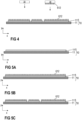
Figure 4 is a cross-sectional view of a substrate arrangement according to one example. -
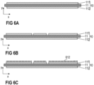
Figure 5 , includingFigure 5A to 5C , schematically illustrates a method for forming a substrate arrangement according to one example. -
Figure 6 , includingFigures 6A to 6C , schematically illustrates a method for forming a substrate arrangement according to another example. -
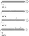
Figure 7 , includingFigures 7A to 7D , schematically illustrates a method for forming a substrate arrangement according to an even further example. -
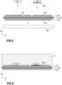
Figure 8 is a cross-sectional view of a substrate arrangement according to another example. -
Figure 9 is a cross-sectional view of a substrate arrangement according to one example with an encapsulant arranged thereon. - In the following detailed description, reference is made to the accompanying drawings. The drawings show specific examples in which the invention may be practiced. It is to be understood that the features and principles described with respect to the various examples may be combined with each other, unless specifically noted otherwise. In the description, as well as in the claims, designations of certain elements as "first element", "second element", "third element" etc. are not to be understood as enumerative. Instead, such designations serve solely to address different "elements". That is, e.g., the existence of a "third element" does not require the existence of a "first element" and a "second element". An electrical line or electrical connection as described herein may be a single electrically conductive element, or include at least two individual electrically conductive elements connected in series and/or parallel. Electrical lines and electrical connections may include metal and/or semiconductor material, and may be permanently electrically conductive (i.e., non-switchable). A semiconductor body as described herein may be made from (doped) semiconductor material and may be a semiconductor chip or be included in a semiconductor chip. A semiconductor body has electrically connecting pads and includes at least one semiconductor element with electrodes.
- Referring to
Figure 1 , a cross-sectional view of a powersemiconductor module arrangement 100 is schematically illustrated. The powersemiconductor module arrangement 100 includes ahousing 7 and asubstrate 10. Thesubstrate 10 includes adielectric insulation layer 11, a (structured)first metallization layer 111 attached to thedielectric insulation layer 11, and a (structured)second metallization layer 112 attached to thedielectric insulation layer 11. Thedielectric insulation layer 11 is disposed between the first andsecond metallization layers - Each of the first and
second metallization layers substrate 10 may be a ceramic substrate, that is, a substrate in which thedielectric insulation layer 11 is a ceramic, e.g., a thin ceramic layer. The ceramic may consist of or include one of the following materials: aluminum oxide; aluminum nitride; zirconium oxide; silicon nitride; boron nitride; or any other dielectric ceramic. For example, thedielectric insulation layer 11 may consist of or include one of the following materials: Al2O3, AIN, SiC, BeO or Si3N4. For instance, thesubstrate 10 may, e.g., be a Direct Copper Bonding (DCB) substrate, a Direct Aluminum Bonding (DAB) substrate, or an Active Metal Brazing (AMB) substrate. Further, thesubstrate 10 may be an Insulated Metal Substrate (IMS). An Insulated Metal Substrate generally comprises adielectric insulation layer 11 comprising (filled) materials such as epoxy resin or polyimide, for example. The material of thedielectric insulation layer 11 may be filled with ceramic particles, for example. Such particles may comprise, e.g., SiO2, Al2O3, AIN, or BN and may have a diameter of between about 1µm and about 50µm. Thesubstrate 10 may also be a conventional printed circuit board (PCB) having a non-ceramicdielectric insulation layer 11. For instance, a non-ceramicdielectric insulation layer 11 may consist of or include a cured resin. - The
substrate 10 is arranged in ahousing 7. In the example illustrated inFigure 1 , thesubstrate 10 is arranged on abase plate 12 which forms a ground surface of thehousing 7, while thehousing 7 itself solely comprises sidewalls and a cover or lid. This is, however, only an example. It is also possible that thehousing 7 further comprises a ground surface and thesubstrate 10 and thebase plate 12 be arranged inside thehousing 7. In some powersemiconductor module arrangements 100, more than onesubstrate 10 is arranged on asingle base plate 12 or on the ground surface of ahousing 7. It is, however, also possible that the powersemiconductor module arrangement 100 does not comprise abase plate 12 at all. For example, thesubstrate 10 may form a ground surface of thehousing 7 instead. It is also possible that thehousing 7 comprises a ground surface, sidewalls and a cover, and one ormore substrates 10 are arranged on the ground surface and inside thehousing 7. That is, the power semiconductor module arrangement may be an arrangement comprising abase plate 12, or a base plate-less powersemiconductor module arrangement 100. - One or
more semiconductor bodies 20 may be arranged on the at least onesubstrate 10. Each of thesemiconductor bodies 20 arranged on the at least onesubstrate 10 may include a diode, an IGBT (Insulated-Gate Bipolar Transistor), a MOSFET (Metal-Oxide-Semiconductor Field-Effect Transistor), a JFET (Junction Field-Effect Transistor), a HEMT (High-Electron-Mobility Transistor), and/or any other suitable semiconductor element. - The one or
more semiconductor bodies 20 may form a semiconductor arrangement on thesubstrate 10. InFigure 1 , only twosemiconductor bodies 20 are exemplarily illustrated. Thesecond metallization layer 112 of thesubstrate 10 inFigure 1 is a continuous layer. Thefirst metallization layer 111 is a structured layer in the example illustrated inFigure 1 . "Structured layer" means that thefirst metallization layer 111 is not a continuous layer, but includes recesses between different sections of the layer. Such recesses are schematically illustrated inFigure 1 . Thefirst metallization layer 111 in this example includes three different sections. This, however, is only an example. Any other number of sections is possible.Different semiconductor bodies 20 may be mounted to the same or to different sections of thefirst metallization layer 111. Different sections of thefirst metallization layer 111 may have no electrical connection or may be electrically connected to one or more other sections using electrical connections 3 such as, e.g., bonding wires. Electrical connections 3 may also include connection plates or conductor rails, for example, to name just a few examples. The one ormore semiconductor bodies 20 may be electrically and mechanically connected to thesubstrate 10 by an electricallyconductive connection layer 30. Such an electricallyconductive connection layer 30 may be a solder layer, a layer of an electrically conductive adhesive, or a layer of a sintered metal powder, e.g., a sintered silver powder, for example. - According to other examples, it is also possible that the
second metallization layer 112 is a structured layer. It is further possible to omit thesecond metallization layer 112 altogether. It is generally also possible that thefirst metallization layer 111 is a continuous layer, for example. - The power
semiconductor module arrangement 100 illustrated inFigure 1 further includesterminal elements 4. Theterminal elements 4 are electrically connected to thefirst metallization layer 111 and provide an electrical connection between the inside and the outside of thehousing 7. Theterminal elements 4 may be electrically connected to thefirst metallization layer 111 with afirst end 41, while asecond end 42 of each of theterminal elements 4 protrudes out of thehousing 7. Theterminal elements 4 may be electrically contacted from the outside at their respective second ends 42. A first part of theterminal elements 4 may extend through the inside of thehousing 7 in a vertical direction y. The vertical direction y is a direction perpendicular to a top surface of thesubstrate 10, wherein the top surface of thesubstrate 10 is a surface on which the at least onesemiconductor body 20 is mounted. Theterminal elements 4 illustrated inFigure 1 , however, are only examples.Terminal elements 4 may be implemented in any other way and may be arranged anywhere within thehousing 7. For example, one or moreterminal elements 4 may be arranged close to or adjacent to the sidewalls of thehousing 7.Terminal elements 4 could also protrude through the sidewalls of thehousing 7 instead of through the cover. Thefirst end 41 of aterminal element 4 may be electrically and mechanically connected to thesubstrate 10 by an electrically conductive connection layer, for example (not explicitly illustrated inFigure 1 ). Such an electrically conductive connection layer may be a solder layer, a layer of an electrically conductive adhesive, or a layer of a sintered metal powder, e.g., a sintered silver (Ag) powder, for example. Thefirst end 41 of aterminal element 4 may also be electrically coupled to thesubstrate 10 via one or more electrical connections 3, for example. For example, the second ends 42 of theterminal elements 4 may be connected to a printed circuit board that is arranged outside of the housing 7 (not illustrated inFigure 1 ). - The power
semiconductor module arrangement 100 further includes anencapsulant 5. Theencapsulant 5 consists of or includes a silicone gel for example. Theencapsulant 5 may at least partly fill the interior of thehousing 7, thereby covering the components and electrical connections that are arranged on thesubstrate 10. Theterminal elements 4 may be partly embedded in theencapsulant 5. At least their second ends 42, however, are not covered by theencapsulant 5 and protrude from theencapsulant 5 through thehousing 7 to the outside of thehousing 7. Theencapsulant 5 is configured to protect the components and electrical connections of thepower semiconductor module 100, in particular the components arranged on thesubstrate 10 inside thehousing 7, from certain environmental conditions and mechanical damage. - As has been described above, different components (e.g.,
semiconductor bodies 20,terminal elements 4 or any other components) may be mounted to the substrate 10 (i.e. the first metallization layer 111) by means of an electricallyconductive connection layer 30. Such an electricallyconductive connection layer 30, however, may have several drawbacks. For example, a plurality of different steps may have to be performed when forming an electrically conductive connection layer 30 (e.g., solder layer, a layer of an electrically conductive adhesive, or a layer of a sintered metal powder). - Now referring to
Figure 2 , afirst connection partner 610 and asecond connection partner 620 are schematically illustrated. Thefirst connection partner 610 may be a substrate for a power semiconductor module, for example. Thesecond connection partner 620 may be a semiconductor body, a terminal element, or any other component that is to be mounted to the substrate, for example. It is, however, also possible that thefirst connection partner 610 is a heat sink or base plate, and thesecond connection partner 620 is a substrate. A plurality ofnanowires 612 is formed on a surface of thefirst connection partner 610 which faces thesecond connection partner 620. A second plurality ofnanowires 612 is formed on a surface of thesecond connection partner 620 which faces thefirst connection partner 610. Each of the plurality ofnanowires 612 has a first end and a second end. A first end of each of the plurality ofnanowires 612 is inseparably connected to the surface of thefirst connection partner 610. A first end of each of the second plurality ofnanowires 612 is inseparably connected to the surface of the second connection partner. The first andsecond connection partners nanowires 612 and the second ends of the second plurality ofnanowires 612 are free ends. The surface of thefirst connection partner 610 on which the plurality ofnanowires 612 is formed and the surface of thesecond connection partner 620 on which the second plurality ofnanowires 612 is formed may consist of the same material such as, e.g., Al, an Al alloy, Cu, a Cu alloy, Ag, an Ag alloy, Au, or an Au alloy. - The
first connection partner 610 and thesecond connection partner 620 are then moved towards each other such that the second ends of the plurality ofnanowires 612 contact the surface of thesecond connection partner 620, and the second ends of the second plurality ofnanowires 612 contact the surface of thefirst connection partner 610. Under the influence of pressure and heat, the second ends of the plurality ofnanowires 612 may be inseparably connected to the surface of thesecond connection partner 620, and the second ends of the second plurality ofnanowires 612 may be inseparably connected to the surface of thefirst connection partner 610. In this way, a permanent connection between thefirst connection partner 610 and thesecond connection partner 620 may be formed by means of thenanowires 612. - The
term nanowires 612 as used herein designates any element having the form of a wire, i.e. a length that is several times larger than its diameter, wherein the dimensions of the element are in the nanometer range. For example, so-called nanotubes or nanorods may also be used and are considered to fall under the term nanowire as used herein. Generally speaking, ananowire 612 is a nanostructure in the form of a wire having a nanorange diameter. For example, a diameter of ananowire 612 may be between 500nm and 1200nm. Thenanowires 612 may have a length between their first end and their second end of between 10µm and 70µm, for example. Thenanowires 612 generally extend perpendicular to the surface on which they are formed. Therefore, allnanowires 612 may have the same length such that the second ends of all of thenanowires 612 extend all the way to the surface of the other connection partner. Thenanowires 612 may comprise or consist of carbon, cobalt, copper, silicon, or gold, for example. -
Nanowires 612 may be formed by any suitable process such as, e.g., (chemical) vapor deposition, suspension, electrochemical deposition, VLS growth (VLS = Vapor-liquid-solid method), and ion track technology. - In the example illustrated in
Figure 2 , the first and thesecond connection partners nanowires 612. This, however, is only an example. As is schematically illustrated inFigure 3A , it is also possible to formnanowires 612 only on one of the two connection partners. In the example illustrated inFigure 2B , the plurality ofnanowires 612 formed on thefirst connection partner 610 and the second plurality ofnanowires 612 formed on thesecond connection partner 620 can be considered to intertwine when the first andsecond connection partner connection partners Figure 3B , because nonanowires 612 are formed on the surface of thesecond connection partner 620. However, with the plurality ofnanowires 612 formed on thefirst connection partner 610, it is still possible to form a permanent connection between thefirst connection partner 610 and thesecond connection partner 620. The stability of the connection, however, may be further improved ifnanowires 612 are provided on both surfaces. - Now referring to
Figure 4 , a substrate arrangement according to one example is schematically illustrated. The substrate arrangement may comprise asubstrate 10, similar to what has been described with respect toFigure 1 above. Thedielectric insulation layer 11, however, may also be omitted. Themetallization layer 111, for example, may also be a so-called lead frame (die pad). That is, the substrate arrangement may solely comprise ametallization layer 111 and nodielectric insulation layer 11. Thesubstrate 10 that is schematically illustrated inFigure 4 comprises adielectric insulation layer 11 and afirst metallization layer 111 attached to a first side of thedielectric insulation layer 11. Thesubstrate 10, optionally, may further comprise a second metallization layer (not specifically illustrated inFigure 4 ). The substrate arrangement further comprises a plurality ofnanowires 612 arranged on a surface of thefirst metallization layer 111. If themetallization layer 111 is arranged on adielectric insulation layer 11, the plurality ofnanowires 612 is arranged on a surface of thefirst metallization layer 111 that faces away from thedielectric insulation layer 11. The plurality ofnanowires 612 is evenly distributed over a section of the surface area or over the entire surface area of thefirst metallization layer 111. That is, the number ofnanowires 612 per unit area is the same over at least a section of the entire surface area of thefirst metallization layer 111. According to one example, the section of the surface area of thefirst metallization layer 111 covered by the plurality ofnanowires 612 is between 60% and 100%, or between 70% and 100% of the entire surface area of thefirst metallization layer 111. In the example illustrated inFigure 4 , thefirst metallization layer 111 is a structured layer. All of the different sections of thefirst metallization layer 111 may be entirely covered bynanowires 612. It is, however, also possible that one or more, but not all sections of thefirst metallization layer 111 remain free ofnanowires 612. Additionally or alternatively it is also possible that one or more sections are only partly covered bynanowires 612. - The
nanowires 612 are generally formed on thefirst metallization layer 111 before any components (e.g.,semiconductor bodies 20,terminal elements 4, or any other components) are arranged on thesubstrate 10. By covering at least a (large) section or even the entire surface area of thefirst metallization layer 111 withnanowires 612, thesubstrate 10 may be equipped with components very flexibly. The section that is covered by thenanowires 612 is larger than the area required for mounting thecomponents metallization layer 111. In this way, the components that are to be arranged on thesubstrate 10 do not have to be mounted to any specifically dedicated areas. That is, the substrate arrangement can be sold to different customers, irrespective of the specific design of the customer. Or the same customer may use the same substrate for different designs without the need for any adaptions or customizations. After anysemiconductor bodies 20 and/or other components have been mounted to thesubstrate 10, a different subset of the plurality ofnanowires 612 is arranged between each of the at least onecomponent first metallization layer 111, wherein the second end of eachnanowire 612 of the at least one subset is inseparably connected to a surface of therespective component nanowires 612 forms a permanent connection between therespective component first metallization layer 111. - The number of
nanowires 612 comprised in the at least one subset ofnanowires 612, however, is less than the number ofnanowires 612 comprised in the plurality ofnanowires 612. That is, the second ends of at least one other subset ofnanowires 612 are free ends that are not connected to anycomponent - A method for producing a substrate arrangement according to one example comprises forming a
first metallization layer 111, forming a plurality ofnanowires 612 on a surface of thefirst metallization layer 111, and arranging at least onecomponent first metallization layer 111 such that a first subset of the plurality of nanowires is arranged between the first metallization layer and the at least one component, wherein the plurality ofnanowires 612 is evenly distributed over a section of the surface area or over the entire surface area of thefirst metallization layer 111, each of the plurality ofnanowires 612 comprises a first end and a second end, wherein the first end of each of theplurality nanowires 612 is inseparably connected to the surface of thefirst metallization layer 111, the second end of each nanowire of the first subset is inseparably connected to a surface of one of the at least onecomponent first metallization layer 111 and the at least onecomponent semiconductor body 20, and the number ofnanowires 612 comprised in the first subset ofnanowires 612 is less than the number ofnanowires 612 comprised in the plurality ofnanowires 612. - In the example illustrated in
Figure 5 , asubstrate 10 comprising adielectric insulation layer 11 and a continuousfirst metallization layer 111 is provided (Figure 5A ), and the plurality ofnanowires 612 is formed on the continuous first metallization layer 111 (Figure 5B ). Thefirst metallization layer 111 in this example is only structured after forming the plurality ofnanowires 612, as is schematically illustrated inFigure 5C . - According to another example, however, and as is schematically illustrated in
Figure 6 , it is alternatively also possible to provide asubstrate 10 comprising adielectric insulation layer 11 and a continuous first metallization layer 111 (Figure 6A ), and to structure the first metallization layer 111 (Figure 6B ) before forming the plurality of nanowires 612 (Figure 6C ). When structuring thefirst metallization layer 111, two or more separate sections and recesses between different sections of thefirst metallization layer 111 are formed. - As has been described above, different methods can be used to form the
nanowires 612. With most methods,nanowires 612 can only be formed on metallic surfaces. Therefore, if thefirst metallization layer 111 is structured first, as is exemplarily illustrated inFigure 6 , generally nonanowires 612 will form on those sections of thedielectric insulation layer 11, which are no longer covered by thefirst metallization layer 111. As has been described with respect toFigure 1 above, thedielectric insulation layer 11 generally does not comprise any metallic surfaces. Therefore, nonanowires 612 will grow on the surfaces of thedielectric insulation layer 11. - According to another example, however, it is also possible to form a
masking layer 70 after structuring the first metallization layer (seeFigure 7B ) and before forming the plurality ofnanowires 612, as is schematically illustrated inFigure 7C . In particular, themasking layer 70 may be formed on those sections of thedielectric insulation layer 11 that are not covered by thefirst metallization layer 111, thereby preventingnanowires 612 from being formed on thedielectric insulation layer 11. Once thenanowires 612 have been formed, themasking layer 70 may be removed (not specifically illustrated). - Now referring to
Figure 8 , components such as, e.g.,semiconductor bodies 20, may be mounted on the surface of thefirst metallization layer 111.Such components 20 may be fitted withnanowires 612 as well, as has been described with respect toFigure 2 above and as is exemplarily illustrated for the semiconductor body on the right hand side ofFigure 8 . This, however, is not mandatory. As has been described with respect toFigure 3 above and as is exemplarily illustrated on the left hand side ofFigure 8 , it is also possible that nonanowires 612 are formed on a surface of the component that is to be mounted to thesubstrate 10. As has been described with respect toFigures 2 and 3 above, the components may be mounted to thesubstrate 10 under the influence of heat and pressure. No additional solder pastes or sinter pastes are generally required. However, it is also possible to form an additional electricallyconductive connection layer 30 between one or more of thecomponents first metallization layer 111, similar to what has been described with respect toFigure 1 above and as is schematically illustrated for thesemiconductor body 20 on the left hand side ofFigure 8 . Such an electricallyconductive connection layer 30 may be formed only regionally. In particular, electrically conductive connection layers 30 may only be formed in those areas that are arranged between thefirst metallization layer 111 and one of thecomponents conductive connection layer 30 fills any gaps or spaces between the respective ones of thenanowires 612 and may even further increase the strength of the connection formed between thefirst metallization layer 111 and therespective component conductive connection layer 30. - Optionally, as is schematically illustrated in
Figure 8 , the substrate arrangement may further comprise asecond metallization layer 112 attached to a second side of thedielectric insulation layer 11 opposite the first side, and a second plurality ofnanowires 612 arranged on a surface of thesecond metallization layer 112 that faces away from thedielectric insulation layer 11, wherein the second plurality ofnanowires 612 is evenly distributed over the entire surface of the second metallization layer 112 (the number ofnanowires 612 per unit area is the same over the entire surface of the second metallization layer 112), and each of the second plurality ofnanowires 612 comprises a first end and a second end, wherein the first end of each of thesecond plurality nanowires 612 is inseparably connected to the surface of thesecond metallization layer 112. The second plurality ofnanowires 612 may be used to form a permanent connection between thesubstrate 10 and a heat sink orbase plate 80, for example. - As has been described above, forming
nanowires 612 over a (large) section or over the entire surface area of thefirst metallization layer 111 allows using thesubstrate 10 very flexibly, as it is not limited to specific designs. Thenanowires 612, however, provide further advantages. As has been described with respect toFigure 1 above, power semiconductor modules often comprise anencapsulant 5 configured to protect the components and electrical connections of the power semiconductor module, in particular the components arranged on thesubstrate 10 inside a housing, from certain environmental conditions and mechanical damage. A substrate arrangement comprising asubstrate 10 withnanowires 612 formed thereon and anencapsulant 5 is schematically illustrated inFigure 9 . - The
encapsulant 5 is generally formed after thecomponents substrate 10. Theencapsulant 5 is formed by filling a liquid or viscous material into a housing (not specifically illustrated inFigure 9 ) and by curing the originally liquid or viscous material, e.g., under the influence of heat and optionally pressure. When the liquid or viscous material of theencapsulant 5 is filled into a housing to cover thesubstrate 10, the material directly adjoins the free second ends of a second subset of the plurality of nanowires (the second subset includingdifferent nanowires 612 than the first subset) and also fills any gaps and spaces between the different ones of the plurality ofnanowires 612 of the second subset. When curing the material, a connection is formed between theencapsulant 5 and thenanowires 612 of the second subset. That is, the encapsulant adheres to thenanowires 612 of the second subset, and therefore to the surface of thefirst metallization layer 111, without the need for any additional adhesion promoters.
Claims (14)
- A substrate arrangement comprises,a first metallization layer (111);a plurality of nanowires (612) arranged on a surface of the first metallization layer (111); andat least one component (20, 4) arranged on the first metallization layer (111) such that a first subset of the plurality of nanowires (612) is arranged between the first metallization layer (111) and the at least one component (20, 4), whereinthe plurality of nanowires (612) is evenly distributed over a section of the surface area or over the entire surface area of the first metallization layer (111),each of the plurality of nanowires (612) comprises a first end and a second end, wherein the first end of each of the plurality nanowires (612) is inseparably connected to the surface of the first metallization layer (111),the second end of each nanowire of the first subset is inseparably connected to a surface of one of the at least one component (20, 4) such that the first subset of nanowires (612) forms a permanent connection between the first metallization layer (111) and the at least one component (20, 4),the at least one component (20, 4) comprises at least one semiconductor body (20),the number of nanowires (612) comprised in the first subset of nanowires (612) is less than the number of nanowires (612) comprised in the plurality of nanowires (612), andthe substrate arrangement further comprises an encapsulant (5), wherein the encapsulant (5) consists of or includes a silicone gel and directly adjoins the second ends of a second subset of the plurality of nanowires (612) and fills any gaps and spaces between the nanowires of the second subset.
- The substrate arrangement of claim 1, wherein the section of the surface area of the first metallization layer (111) covered by the plurality of nanowires (612) is between 60% and 100%, or between 70% and 100% of the entire surface area of the first metallization layer (111).
- The substrate arrangement of claim 1 or 2, further comprising a dielectric insulation layer (11), wherein the first metallization layer (111) is attached to a first side of the dielectric insulation layer (11).
- The substrate arrangement of claim 3, further comprisinga second metallization layer (112) attached to a second side of the dielectric insulation layer (11) opposite the first side; anda second plurality of nanowires (612) arranged on a surface of the second metallization layer (112) that faces away from the dielectric insulation layer (11), whereinthe second plurality of nanowires (612) is evenly distributed over the entire surface of the second metallization layer (112), andeach of the second plurality of nanowires (612) comprises a first end and a second end, wherein the first end of each of the second plurality nanowires (612) is inseparably connected to the surface of the second metallization layer (112).
- The substrate arrangement of any of claims 1 to 4, wherein the first metallization layer (111) is a structured layer comprising two or more separate sections, and recesses between different sections of the first metallization layer (111).
- The substrate arrangement of any of claims 1 to 5, wherein each of the plurality of nanowires (612) has a diameter of between 500nm and 1200nm.
- The substrate arrangement of any of claims 1 to 6, wherein all of the plurality of nanowires (612) have an equal length between their first end and their second end of between 10µm and 70µm.
- The substrate arrangement of any of the preceding claims, wherein the first metallization layer (111) comprises or consists of copper, a copper alloy, aluminum, or an aluminum alloy.
- The substrate arrangement of any of the preceding claims, wherein the plurality of nanowires (612) comprises or consists of carbon, cobalt, copper, silicon, or gold.
- A method comprising:forming a first metallization layer (111);forming a plurality of nanowires (612) on a surface of the first metallization layer (111); andarranging at least one component (20, 4) on the first metallization layer (111) such that a first subset of the plurality of nanowires (612) is arranged between the first metallization layer (111) and the at least one component (20, 4), whereinthe plurality of nanowires (612) is evenly distributed over a section of the surface area or over the entire surface area of the first metallization layer (111),each of the plurality of nanowires (612) comprises a first end and a second end, wherein the first end of each of the plurality nanowires (612) is inseparably connected to the surface of the first metallization layer (111),the second end of each nanowire of the first subset is inseparably connected to a surface of one of the at least one component (20, 4) such that the first subset of nanowires (612) forms a permanent connection between the first metallization layer (111) and the at least one component (20, 4),the at least one component (20, 4) comprises at least one semiconductor body (20),the number of nanowires (612) comprised in the first subset of nanowires (612) is less than the number of nanowires (612) comprised in the plurality of nanowires (612), andthe method further comprises forming an encapsulant (5), wherein the encapsulant (5) consists of or includes a silicone gel and directly adjoins the second ends of a second subset of the plurality of nanowires (612) and fills any gaps and spaces between the nanowires of the second subset.
- The method of claim 10, further comprising
structuring the first metallization layer (111), thereby forming two or more separate sections and recesses between different sections of the first metallization layer (111). - The method of claim 11, wherein
the first metallization layer (111) is structured after forming the plurality of nanowires (612). - The method of claim 11, wherein
the first metallization layer (111) is structured before forming the plurality of nanowires (612). - The method of claim 13, further comprising
after structuring the first metallization layer (111) and before forming the plurality of nanowires (612), forming a masking layer (70) in the recesses between different sections of the first metallization layer (111).
Priority Applications (3)
| Application Number | Priority Date | Filing Date | Title |
|---|---|---|---|
| EP22207915.4A EP4372807B1 (en) | 2022-11-16 | 2022-11-16 | Substrate arrangement and methods for producing a substrate arrangement |
| US18/504,309 US20240162129A1 (en) | 2022-11-16 | 2023-11-08 | Substrate arrangement and methods for producing a substrate arrangement |
| CN202311485955.6A CN118053849A (en) | 2022-11-16 | 2023-11-09 | Substrate device and method for producing substrate device |
Applications Claiming Priority (1)
| Application Number | Priority Date | Filing Date | Title |
|---|---|---|---|
| EP22207915.4A EP4372807B1 (en) | 2022-11-16 | 2022-11-16 | Substrate arrangement and methods for producing a substrate arrangement |
Publications (2)
| Publication Number | Publication Date |
|---|---|
| EP4372807A1 EP4372807A1 (en) | 2024-05-22 |
| EP4372807B1 true EP4372807B1 (en) | 2024-10-16 |
Family
ID=84365438
Family Applications (1)
| Application Number | Title | Priority Date | Filing Date |
|---|---|---|---|
| EP22207915.4A Active EP4372807B1 (en) | 2022-11-16 | 2022-11-16 | Substrate arrangement and methods for producing a substrate arrangement |
Country Status (3)
| Country | Link |
|---|---|
| US (1) | US20240162129A1 (en) |
| EP (1) | EP4372807B1 (en) |
| CN (1) | CN118053849A (en) |
Citations (10)
| Publication number | Priority date | Publication date | Assignee | Title |
|---|---|---|---|---|
| US7327037B2 (en) | 2004-04-01 | 2008-02-05 | Lucent Technologies Inc. | High density nanostructured interconnection |
| DE102017104922A1 (en) | 2017-03-08 | 2018-09-13 | Olav Birlem | Connection of electrical conductors |
| WO2018162682A1 (en) | 2017-03-08 | 2018-09-13 | Technische Universität Darmstadt | System and method for providing a plurality of nanowires and galvanic capsule |
| DE102017104923A1 (en) | 2017-03-08 | 2018-09-13 | Olav Birlem | Connection for a semiconductor chip |
| DE102017104921A1 (en) | 2017-03-08 | 2018-09-13 | Olav Birlem | Connection of thermal conductors |
| EP3511977A1 (en) | 2018-01-16 | 2019-07-17 | Infineon Technologies AG | Semiconductor module and method for producing the same |
| US20200321302A1 (en) | 2019-04-08 | 2020-10-08 | Texas Instruments Incorporated | Nanowires plated on nanoparticles |
| EP3859775A1 (en) | 2020-02-03 | 2021-08-04 | Infineon Technologies AG | Semiconductor arrangement and method for producing the same |
| DE102020215534A1 (en) | 2020-12-09 | 2022-06-09 | Robert Bosch Gesellschaft mit beschränkter Haftung | Electrical and/or electronic assembly and method for producing an electrical and/or electronic assembly |
| EP4084062A1 (en) | 2021-04-30 | 2022-11-02 | Infineon Technologies AG | Power semiconductor module arrangement |
Family Cites Families (2)
| Publication number | Priority date | Publication date | Assignee | Title |
|---|---|---|---|---|
| TWI287805B (en) * | 2005-11-11 | 2007-10-01 | Ind Tech Res Inst | Composite conductive film and semiconductor package using such film |
| JP5051243B2 (en) * | 2008-02-15 | 2012-10-17 | 富士通株式会社 | Manufacturing method of semiconductor device |
-
2022
- 2022-11-16 EP EP22207915.4A patent/EP4372807B1/en active Active
-
2023
- 2023-11-08 US US18/504,309 patent/US20240162129A1/en active Pending
- 2023-11-09 CN CN202311485955.6A patent/CN118053849A/en active Pending
Patent Citations (10)
| Publication number | Priority date | Publication date | Assignee | Title |
|---|---|---|---|---|
| US7327037B2 (en) | 2004-04-01 | 2008-02-05 | Lucent Technologies Inc. | High density nanostructured interconnection |
| DE102017104922A1 (en) | 2017-03-08 | 2018-09-13 | Olav Birlem | Connection of electrical conductors |
| WO2018162682A1 (en) | 2017-03-08 | 2018-09-13 | Technische Universität Darmstadt | System and method for providing a plurality of nanowires and galvanic capsule |
| DE102017104923A1 (en) | 2017-03-08 | 2018-09-13 | Olav Birlem | Connection for a semiconductor chip |
| DE102017104921A1 (en) | 2017-03-08 | 2018-09-13 | Olav Birlem | Connection of thermal conductors |
| EP3511977A1 (en) | 2018-01-16 | 2019-07-17 | Infineon Technologies AG | Semiconductor module and method for producing the same |
| US20200321302A1 (en) | 2019-04-08 | 2020-10-08 | Texas Instruments Incorporated | Nanowires plated on nanoparticles |
| EP3859775A1 (en) | 2020-02-03 | 2021-08-04 | Infineon Technologies AG | Semiconductor arrangement and method for producing the same |
| DE102020215534A1 (en) | 2020-12-09 | 2022-06-09 | Robert Bosch Gesellschaft mit beschränkter Haftung | Electrical and/or electronic assembly and method for producing an electrical and/or electronic assembly |
| EP4084062A1 (en) | 2021-04-30 | 2022-11-02 | Infineon Technologies AG | Power semiconductor module arrangement |
Non-Patent Citations (1)
| Title |
|---|
| XU JIAYU, XUEBAO LI, XIANG CUI, ZHIBIN ZHAO, SHENYANG MO, BING JI: "Trap Characteristics and Their Temperature-dependence of Silicone Gel for Encapsulation in IGBT Power Modules", CSEE JOURNAL OF POWER AND ENERGY SYSTEMS, vol. 7, no. 3, 1 May 2021 (2021-05-01), pages 614 - 621, XP093299311, DOI: 10.17775/CSEEJPES.2020.02840 |
Also Published As
| Publication number | Publication date |
|---|---|
| EP4372807A1 (en) | 2024-05-22 |
| US20240162129A1 (en) | 2024-05-16 |
| CN118053849A (en) | 2024-05-17 |
Similar Documents
| Publication | Publication Date | Title |
|---|---|---|
| US7705436B2 (en) | Semiconductor device with semiconductor chip and method for producing it | |
| CN102593081B (en) | Comprise the semiconductor device of radiator | |
| US8587116B2 (en) | Semiconductor module comprising an insert | |
| US20210013132A1 (en) | Die Attach Methods and Semiconductor Devices Manufactured based on Such Methods | |
| WO1995028740A1 (en) | Electronic package having improved wire bonding capability | |
| US11942449B2 (en) | Semiconductor arrangement and method for producing the same | |
| EP4084062A1 (en) | Power semiconductor module arrangement | |
| EP4372807B1 (en) | Substrate arrangement and methods for producing a substrate arrangement | |
| EP3863045B1 (en) | Power semiconductor module arrangement and method for producing the same | |
| US20230369175A1 (en) | Power semiconductor module arrangement and method for producing the same | |
| EP4307359A1 (en) | Power semiconductor module arrangement and method for producing the same | |
| JPH0645504A (en) | Semiconductor device | |
| US20230170286A1 (en) | Terminal Element or Bus Bar, and Power Semiconductor Module Arrangement Comprising a Terminal Element or Bus Bar | |
| EP3401957B1 (en) | Power semiconductor module arrangement and method for producing the same | |
| EP4601000A1 (en) | Power semiconductor module arrangement and method for producing the same | |
| EP4421868B1 (en) | Semiconductor module arrangement | |
| US20260090317A1 (en) | System and method for mounting a housing to a base plate of a semiconductor module | |
| EP4576199A1 (en) | Substrate and methods for producing a substrate | |
| EP4607584A1 (en) | Semiconductor module arrangement | |
| EP4510184A1 (en) | Terminal element, and power semiconductor module arrangement comprising a terminal element | |
| EP4428914A1 (en) | Power semiconductor module arrangement | |
| EP4270466A1 (en) | Power semiconductor module arrangements and methods for producing power semiconductor module arrangements | |
| EP4651201A1 (en) | Power semiconductor module arrangement and methods for producing the same | |
| EP4607586A1 (en) | Method and system for connecting a terminal element to a substrate | |
| EP4648094A1 (en) | Method for connecting two metal layers and arrangement comprising two metal layers connected to each other |
Legal Events
| Date | Code | Title | Description |
|---|---|---|---|
| PUAI | Public reference made under article 153(3) epc to a published international application that has entered the european phase |
Free format text: ORIGINAL CODE: 0009012 |
|
| STAA | Information on the status of an ep patent application or granted ep patent |
Free format text: STATUS: REQUEST FOR EXAMINATION WAS MADE |
|
| 17P | Request for examination filed |
Effective date: 20230914 |
|
| AK | Designated contracting states |
Kind code of ref document: A1 Designated state(s): AL AT BE BG CH CY CZ DE DK EE ES FI FR GB GR HR HU IE IS IT LI LT LU LV MC ME MK MT NL NO PL PT RO RS SE SI SK SM TR |
|
| GRAP | Despatch of communication of intention to grant a patent |
Free format text: ORIGINAL CODE: EPIDOSNIGR1 |
|
| STAA | Information on the status of an ep patent application or granted ep patent |
Free format text: STATUS: GRANT OF PATENT IS INTENDED |
|
| RIC1 | Information provided on ipc code assigned before grant |
Ipc: H01L 23/498 20060101ALN20240523BHEP Ipc: H01L 23/373 20060101ALN20240523BHEP Ipc: H01L 23/49 20060101ALN20240523BHEP Ipc: H01L 23/24 20060101ALI20240523BHEP Ipc: H01L 23/053 20060101ALI20240523BHEP Ipc: H01L 23/31 20060101ALI20240523BHEP Ipc: H01L 21/48 20060101ALI20240523BHEP Ipc: H01L 25/07 20060101ALI20240523BHEP Ipc: H01L 23/48 20060101AFI20240523BHEP |
|
| RIC1 | Information provided on ipc code assigned before grant |
Ipc: H01L 23/498 20060101ALN20240603BHEP Ipc: H01L 23/373 20060101ALN20240603BHEP Ipc: H01L 23/49 20060101ALN20240603BHEP Ipc: H01L 23/24 20060101ALI20240603BHEP Ipc: H01L 23/053 20060101ALI20240603BHEP Ipc: H01L 23/31 20060101ALI20240603BHEP Ipc: H01L 21/48 20060101ALI20240603BHEP Ipc: H01L 25/07 20060101ALI20240603BHEP Ipc: H01L 23/48 20060101AFI20240603BHEP |
|
| INTG | Intention to grant announced |
Effective date: 20240618 |
|
| P01 | Opt-out of the competence of the unified patent court (upc) registered |
Free format text: CASE NUMBER: APP_42041/2024 Effective date: 20240716 |
|
| GRAS | Grant fee paid |
Free format text: ORIGINAL CODE: EPIDOSNIGR3 |
|
| GRAA | (expected) grant |
Free format text: ORIGINAL CODE: 0009210 |
|
| STAA | Information on the status of an ep patent application or granted ep patent |
Free format text: STATUS: THE PATENT HAS BEEN GRANTED |
|
| AK | Designated contracting states |
Kind code of ref document: B1 Designated state(s): AL AT BE BG CH CY CZ DE DK EE ES FI FR GB GR HR HU IE IS IT LI LT LU LV MC ME MK MT NL NO PL PT RO RS SE SI SK SM TR |
|
| REG | Reference to a national code |
Ref country code: GB Ref legal event code: FG4D |
|
| REG | Reference to a national code |
Ref country code: CH Ref legal event code: EP |
|
| REG | Reference to a national code |
Ref country code: IE Ref legal event code: FG4D |
|
| REG | Reference to a national code |
Ref country code: DE Ref legal event code: R096 Ref document number: 602022006845 Country of ref document: DE |
|
| REG | Reference to a national code |
Ref country code: LT Ref legal event code: MG9D |
|
| REG | Reference to a national code |
Ref country code: NL Ref legal event code: MP Effective date: 20241016 |
|
| REG | Reference to a national code |
Ref country code: AT Ref legal event code: MK05 Ref document number: 1733668 Country of ref document: AT Kind code of ref document: T Effective date: 20241016 |
|
| PG25 | Lapsed in a contracting state [announced via postgrant information from national office to epo] |
Ref country code: NL Free format text: LAPSE BECAUSE OF FAILURE TO SUBMIT A TRANSLATION OF THE DESCRIPTION OR TO PAY THE FEE WITHIN THE PRESCRIBED TIME-LIMIT Effective date: 20241016 |
|
| PG25 | Lapsed in a contracting state [announced via postgrant information from national office to epo] |
Ref country code: NL Free format text: LAPSE BECAUSE OF FAILURE TO SUBMIT A TRANSLATION OF THE DESCRIPTION OR TO PAY THE FEE WITHIN THE PRESCRIBED TIME-LIMIT Effective date: 20241016 |
|
| PG25 | Lapsed in a contracting state [announced via postgrant information from national office to epo] |
Ref country code: HR Free format text: LAPSE BECAUSE OF FAILURE TO SUBMIT A TRANSLATION OF THE DESCRIPTION OR TO PAY THE FEE WITHIN THE PRESCRIBED TIME-LIMIT Effective date: 20241016 Ref country code: IS Free format text: LAPSE BECAUSE OF FAILURE TO SUBMIT A TRANSLATION OF THE DESCRIPTION OR TO PAY THE FEE WITHIN THE PRESCRIBED TIME-LIMIT Effective date: 20250216 Ref country code: PT Free format text: LAPSE BECAUSE OF FAILURE TO SUBMIT A TRANSLATION OF THE DESCRIPTION OR TO PAY THE FEE WITHIN THE PRESCRIBED TIME-LIMIT Effective date: 20250217 |
|
| PGFP | Annual fee paid to national office [announced via postgrant information from national office to epo] |
Ref country code: DE Payment date: 20250123 Year of fee payment: 3 |
|
| PG25 | Lapsed in a contracting state [announced via postgrant information from national office to epo] |
Ref country code: FI Free format text: LAPSE BECAUSE OF FAILURE TO SUBMIT A TRANSLATION OF THE DESCRIPTION OR TO PAY THE FEE WITHIN THE PRESCRIBED TIME-LIMIT Effective date: 20241016 |
|
| PG25 | Lapsed in a contracting state [announced via postgrant information from national office to epo] |
Ref country code: BG Free format text: LAPSE BECAUSE OF FAILURE TO SUBMIT A TRANSLATION OF THE DESCRIPTION OR TO PAY THE FEE WITHIN THE PRESCRIBED TIME-LIMIT Effective date: 20241016 |
|
| PG25 | Lapsed in a contracting state [announced via postgrant information from national office to epo] |
Ref country code: ES Free format text: LAPSE BECAUSE OF FAILURE TO SUBMIT A TRANSLATION OF THE DESCRIPTION OR TO PAY THE FEE WITHIN THE PRESCRIBED TIME-LIMIT Effective date: 20241016 |
|
| PG25 | Lapsed in a contracting state [announced via postgrant information from national office to epo] |
Ref country code: NO Free format text: LAPSE BECAUSE OF FAILURE TO SUBMIT A TRANSLATION OF THE DESCRIPTION OR TO PAY THE FEE WITHIN THE PRESCRIBED TIME-LIMIT Effective date: 20250116 |
|
| PG25 | Lapsed in a contracting state [announced via postgrant information from national office to epo] |
Ref country code: LV Free format text: LAPSE BECAUSE OF FAILURE TO SUBMIT A TRANSLATION OF THE DESCRIPTION OR TO PAY THE FEE WITHIN THE PRESCRIBED TIME-LIMIT Effective date: 20241016 Ref country code: AT Free format text: LAPSE BECAUSE OF FAILURE TO SUBMIT A TRANSLATION OF THE DESCRIPTION OR TO PAY THE FEE WITHIN THE PRESCRIBED TIME-LIMIT Effective date: 20241016 Ref country code: GR Free format text: LAPSE BECAUSE OF FAILURE TO SUBMIT A TRANSLATION OF THE DESCRIPTION OR TO PAY THE FEE WITHIN THE PRESCRIBED TIME-LIMIT Effective date: 20250117 |
|
| PG25 | Lapsed in a contracting state [announced via postgrant information from national office to epo] |
Ref country code: PL Free format text: LAPSE BECAUSE OF FAILURE TO SUBMIT A TRANSLATION OF THE DESCRIPTION OR TO PAY THE FEE WITHIN THE PRESCRIBED TIME-LIMIT Effective date: 20241016 |
|
| PG25 | Lapsed in a contracting state [announced via postgrant information from national office to epo] |
Ref country code: RS Free format text: LAPSE BECAUSE OF FAILURE TO SUBMIT A TRANSLATION OF THE DESCRIPTION OR TO PAY THE FEE WITHIN THE PRESCRIBED TIME-LIMIT Effective date: 20250116 |
|
| PG25 | Lapsed in a contracting state [announced via postgrant information from national office to epo] |
Ref country code: SM Free format text: LAPSE BECAUSE OF FAILURE TO SUBMIT A TRANSLATION OF THE DESCRIPTION OR TO PAY THE FEE WITHIN THE PRESCRIBED TIME-LIMIT Effective date: 20241016 |
|
| PG25 | Lapsed in a contracting state [announced via postgrant information from national office to epo] |
Ref country code: MC Free format text: LAPSE BECAUSE OF FAILURE TO SUBMIT A TRANSLATION OF THE DESCRIPTION OR TO PAY THE FEE WITHIN THE PRESCRIBED TIME-LIMIT Effective date: 20241016 |
|
| PG25 | Lapsed in a contracting state [announced via postgrant information from national office to epo] |
Ref country code: DK Free format text: LAPSE BECAUSE OF FAILURE TO SUBMIT A TRANSLATION OF THE DESCRIPTION OR TO PAY THE FEE WITHIN THE PRESCRIBED TIME-LIMIT Effective date: 20241016 |
|
| REG | Reference to a national code |
Ref country code: DE Ref legal event code: R026 Ref document number: 602022006845 Country of ref document: DE |
|
| PG25 | Lapsed in a contracting state [announced via postgrant information from national office to epo] |
Ref country code: LU Free format text: LAPSE BECAUSE OF NON-PAYMENT OF DUE FEES Effective date: 20241116 |
|
| PG25 | Lapsed in a contracting state [announced via postgrant information from national office to epo] |
Ref country code: EE Free format text: LAPSE BECAUSE OF FAILURE TO SUBMIT A TRANSLATION OF THE DESCRIPTION OR TO PAY THE FEE WITHIN THE PRESCRIBED TIME-LIMIT Effective date: 20241016 |
|
| PLBI | Opposition filed |
Free format text: ORIGINAL CODE: 0009260 |
|
| PG25 | Lapsed in a contracting state [announced via postgrant information from national office to epo] |
Ref country code: RO Free format text: LAPSE BECAUSE OF FAILURE TO SUBMIT A TRANSLATION OF THE DESCRIPTION OR TO PAY THE FEE WITHIN THE PRESCRIBED TIME-LIMIT Effective date: 20241016 |
|
| PG25 | Lapsed in a contracting state [announced via postgrant information from national office to epo] |
Ref country code: SK Free format text: LAPSE BECAUSE OF FAILURE TO SUBMIT A TRANSLATION OF THE DESCRIPTION OR TO PAY THE FEE WITHIN THE PRESCRIBED TIME-LIMIT Effective date: 20241016 |
|
| PG25 | Lapsed in a contracting state [announced via postgrant information from national office to epo] |
Ref country code: CZ Free format text: LAPSE BECAUSE OF FAILURE TO SUBMIT A TRANSLATION OF THE DESCRIPTION OR TO PAY THE FEE WITHIN THE PRESCRIBED TIME-LIMIT Effective date: 20241016 |
|
| PG25 | Lapsed in a contracting state [announced via postgrant information from national office to epo] |
Ref country code: IT Free format text: LAPSE BECAUSE OF FAILURE TO SUBMIT A TRANSLATION OF THE DESCRIPTION OR TO PAY THE FEE WITHIN THE PRESCRIBED TIME-LIMIT Effective date: 20241016 |
|
| 26 | Opposition filed |
Opponent name: NANOWIRED GMBH Effective date: 20250714 |
|
| PLAX | Notice of opposition and request to file observation + time limit sent |
Free format text: ORIGINAL CODE: EPIDOSNOBS2 |
|
| REG | Reference to a national code |
Ref country code: BE Ref legal event code: MM Effective date: 20241130 |
|
| PG25 | Lapsed in a contracting state [announced via postgrant information from national office to epo] |
Ref country code: SE Free format text: LAPSE BECAUSE OF FAILURE TO SUBMIT A TRANSLATION OF THE DESCRIPTION OR TO PAY THE FEE WITHIN THE PRESCRIBED TIME-LIMIT Effective date: 20241016 |
|
| PG25 | Lapsed in a contracting state [announced via postgrant information from national office to epo] |
Ref country code: BE Free format text: LAPSE BECAUSE OF NON-PAYMENT OF DUE FEES Effective date: 20241130 |
|
| PG25 | Lapsed in a contracting state [announced via postgrant information from national office to epo] |
Ref country code: FR Free format text: LAPSE BECAUSE OF NON-PAYMENT OF DUE FEES Effective date: 20241216 |
|
| PG25 | Lapsed in a contracting state [announced via postgrant information from national office to epo] |
Ref country code: IE Free format text: LAPSE BECAUSE OF NON-PAYMENT OF DUE FEES Effective date: 20241116 |
|
| REG | Reference to a national code |
Ref country code: DE Ref legal event code: R079 Ref document number: 602022006845 Country of ref document: DE Free format text: PREVIOUS MAIN CLASS: H01L0023480000 Ipc: H10W0072000000 |
|
| RDAF | Communication despatched that patent is revoked |
Free format text: ORIGINAL CODE: EPIDOSNREV1 |
|
| PG25 | Lapsed in a contracting state [announced via postgrant information from national office to epo] |
Ref country code: HU Free format text: LAPSE BECAUSE OF FAILURE TO SUBMIT A TRANSLATION OF THE DESCRIPTION OR TO PAY THE FEE WITHIN THE PRESCRIBED TIME-LIMIT; INVALID AB INITIO Effective date: 20221116 |