EP4372526A1 - Devices and methods for communicating a proximity sensor interrupt on a radio frequency transmission line - Google Patents
Devices and methods for communicating a proximity sensor interrupt on a radio frequency transmission line Download PDFInfo
- Publication number
- EP4372526A1 EP4372526A1 EP22207491.6A EP22207491A EP4372526A1 EP 4372526 A1 EP4372526 A1 EP 4372526A1 EP 22207491 A EP22207491 A EP 22207491A EP 4372526 A1 EP4372526 A1 EP 4372526A1
- Authority
- EP
- European Patent Office
- Prior art keywords
- voltage
- port
- circuitry
- bias tee
- antenna
- Prior art date
- Legal status (The legal status is an assumption and is not a legal conclusion. Google has not performed a legal analysis and makes no representation as to the accuracy of the status listed.)
- Granted
Links
Images




Classifications
-
- H—ELECTRICITY
- H04—ELECTRIC COMMUNICATION TECHNIQUE
- H04B—TRANSMISSION
- H04B1/00—Details of transmission systems, not covered by a single one of groups H04B3/00 - H04B13/00; Details of transmission systems not characterised by the medium used for transmission
- H04B1/38—Transceivers, i.e. devices in which transmitter and receiver form a structural unit and in which at least one part is used for functions of transmitting and receiving
- H04B1/3827—Portable transceivers
- H04B1/3833—Hand-held transceivers
- H04B1/3838—Arrangements for reducing RF exposure to the user, e.g. by changing the shape of the transceiver while in use
-
- G—PHYSICS
- G06—COMPUTING OR CALCULATING; COUNTING
- G06F—ELECTRIC DIGITAL DATA PROCESSING
- G06F1/00—Details not covered by groups G06F3/00 - G06F13/00 and G06F21/00
- G06F1/26—Power supply means, e.g. regulation thereof
- G06F1/32—Means for saving power
- G06F1/3203—Power management, i.e. event-based initiation of a power-saving mode
- G06F1/3206—Monitoring of events, devices or parameters that trigger a change in power modality
- G06F1/3231—Monitoring the presence, absence or movement of users
-
- H—ELECTRICITY
- H01—ELECTRIC ELEMENTS
- H01Q—ANTENNAS, i.e. RADIO AERIALS
- H01Q1/00—Details of, or arrangements associated with, antennas
- H01Q1/12—Supports; Mounting means
- H01Q1/22—Supports; Mounting means by structural association with other equipment or articles
- H01Q1/24—Supports; Mounting means by structural association with other equipment or articles with receiving set
- H01Q1/241—Supports; Mounting means by structural association with other equipment or articles with receiving set used in mobile communications, e.g. GSM
- H01Q1/242—Supports; Mounting means by structural association with other equipment or articles with receiving set used in mobile communications, e.g. GSM specially adapted for hand-held use
- H01Q1/243—Supports; Mounting means by structural association with other equipment or articles with receiving set used in mobile communications, e.g. GSM specially adapted for hand-held use with built-in antennas
Definitions
- New communication technologies such as 5G New Radio (NR), WiGig, and Wireless Local Area Networks (WLANs) such as WiFi
- NR 5G New Radio
- WiGig Wireless Local Area Networks
- WLANs Wireless Local Area Networks
- mmWave millimeter wave
- RF radio frequency
- a device uses beamforming to focus high RF transmissions in a narrow direction, the resulting beam may deliver elevated levels of radiation energy to a focused area.
- this focused area is pointed at a user, the device may deliver high levels of harmful radiation to the user and the signal quality may also be significantly degraded.
- the amount of radiation energy emitted absorbed by a unit of mass of a user over time may be defined as the specific absorption rate (SAR).
- SAR specific absorption rate
- Various regulators including the Federal Communications Commission (FCC) and the International Commission on Non-Ionizing Radiation Protection (ICNIRP), and standardization bodies like the 3 rd Generation Partnership Project (3GPP) have introduced SAR measures that limit the amount of radiation that a device can deliver to users.
- FCC Federal Communications Commission
- ICNIRP International Commission on Non-Ionizing Radiation Protection
- 3GPP 3 rd Generation Partnership Project
- Existing SAR proximity sensor implementations can detect human presence and reduce antenna transmission power when human presence is detected near antennas but have various disadvantages.
- the SAR proximity sensor when the SAR proximity sensor detects human presence, the SAR proximity sensor is configured to send an interrupt to a host processor device (e.g., system-on-a-chip (SoC).
- SoC system-on-a-chip
- the host processor device plays a significant role in processing and handling interrupts from the SAR proximity sensor.
- the SAR proximity sensor when the SAR proximity sensor detects human presence, the SAR proximity sensor is configured to send an interrupt to a modem. In such implementations, it is very complicated to provide individual antenna power management in a multiple antenna system.
- FIG. 4 illustrates an exemplary block diagram of an existing SAR proximity sensor implementation 400.
- antennas 405a, 405b are electrically connected to a radio connectivity module (e.g., modem) 490
- a SAR proximity sensor 403 includes proximity sensing electrodes 404a, 404b disposed near antennas 405a, 405b respectively
- a host processor device 480 connected to the proximity sensor 403 and the radio connectivity module 490.
- the host processor device 480 may include an interface hub 483 for communicating with the radio connectivity module 490 and the proximity sensor 403.
- the interface hub 483 may include a sensor hub 481 (e.g., a microcontroller unit/coprocessor/DSP) for receiving and processing data from the proximity sensor 403.
- a sensor hub 481 e.g., a microcontroller unit/coprocessor/DSP
- FIG. 5 illustrates an exemplary block diagram of an existing SAR proximity sensor implementation 500.
- antenna 505 is electrically connected to a radio connectivity module 590
- a SAR proximity sensor 503 includes proximity sensing electrode 504 disposed near antenna 505, and a host processor device 580 connected to the radio connectivity module 590.
- the radio connectivity module 590 may include front-end and RF IC module 591 and a baseband IC module 593.
- the host processor device 580 may also be connected to the sensor 503.
- the host processor device 580 may include an interface hub for communicating with the radio connectivity module 590 and the proximity sensor 503.
- an interrupt pin e.g., DPR pin
- the modem may be asserted by the host processor device 580 (e.g., SoC) or directly by the SAR sensor.
- the proximity sensor 403, 503 is configured to transmit an interrupt to the host processor device 480, 580.
- the interrupt port of the proximity sensor 403, 503 is connected to the interface hub 483 of the host processor device 480, 580.
- the host processor device 480, 580 signals the radio connectivity module 490, 590 to indicate the interrupt condition (i.e., human presence detected)(e.g., SoC triggers a DPR pin of the modem through a GPIO port of the SoC based on an interrupt received on an ISH port of the SoC).
- the interrupt condition i.e., human presence detected
- SoC SoC triggers a DPR pin of the modem through a GPIO port of the SoC based on an interrupt received on an ISH port of the SoC.
- the proximity sensor 403, 503 is configured to transmit an interrupt directly to the modem 490, 590.
- the interrupt port of the proximity sensor 403, 503 is directly connected to an interrupt port of the radio connectivity module 490, 590 (e.g., via a DPR pin). That is, the interrupt is not transmitted to the host processor device 480, 580.
- the disadvantages of current SAR implementations include higher system complexity as the proximity sensor interrupt is connected to the radio module through a sensor hub or from the host processor.
- the proximity sensor interrupt is indirectly asserted to the radio/connectivity module, there is software overhead from the system platform standpoint because the host processor device is involved in the interrupt handling process.
- the proximity sensor interrupt is directly asserted to the radio/connectivity module, multiple interrupt ports at the radio module would be required to support independent antenna power management in a multiple antenna transmission scenario.
- a single interrupt port e.g. DPR pin
- the existing solution cannot distinguish among multiple antenna transmit scenarios and the power back off will be applied to all antennas irrespective of which antenna/antennae detected the proximity.
- the present disclosure provides an innovative way to power the SAR proximity sensor and communicate the sensor interrupt back to the radio/connectivity module using an antenna interconnect (e.g., a connection line between the radio connectivity module and the antenna, i.e., an RF path).
- an antenna interconnect e.g., a connection line between the radio connectivity module and the antenna, i.e., an RF path.
- the proximity detection/interrupt can be communicated to a radio/connectivity module without using or adding additional interconnect pins on the radio/connectivity module interface and without involving the host system.
- the methods and devices provided herein are better able to regulate antenna transmission power and provide numerous advantages in wireless communications systems.
- methods and devices are configured to use a single line for transmitting an RF signal to an antenna, powering a proximity sensor, and communicating an interrupt condition from the proximity sensor to the radio/connectivity module.
- the methods and devices provide that the SAR sensor is connected via a bias tee port.
- the methods and devices of this disclosure provide numerous advantages, including (but not limited to): eliminating involvement of the host processor; simplifying routing and interconnect design; allowing individual power management for multiple antennas.
- plural and “multiple” in the description or the claims expressly refer to a quantity greater than one.
- group (of)”, “set [of]”, “collection (of)”, “series (of)”, “sequence (of)”, “grouping (of)”, etc., and the like in the description or in the claims refer to a quantity equal to or greater than one, i.e. one or more. Any term expressed in plural form that does not expressly state “plurality” or “multiple” likewise refers to a quantity equal to or greater than one.
- the terms “proper subset”, “reduced subset”, and “lesser subset” refer to a subset of a set that is not equal to the set, i.e. a subset of a set that contains less elements than the set.
- any vector and/or matrix notation utilized herein is exemplary in nature and is employed solely for purposes of explanation. Accordingly, aspects of this disclosure accompanied by vector and/or matrix notation are not limited to being implemented solely using vectors and/or matrices, and that the associated processes and computations may be equivalently performed with respect to sets, sequences, groups, etc., of data, observations, information, signals, samples, symbols, elements, etc.
- memory is understood as a non-transitory computer-readable medium in which data or information can be stored for retrieval. References to “memory” included herein may thus be understood as referring to volatile or non-volatile memory, including random access memory (RAM), read-only memory (ROM), flash memory, solid-state storage, magnetic tape, hard disk drive, optical drive, etc., or any combination thereof. Furthermore, registers, shift registers, processor registers, data buffers, etc., are also embraced herein by the term memory. A single component referred to as “memory” or “a memory” may be composed of more than one different type of memory, and thus may refer to a collective component including one or more types of memory.
- memory may be depicted as separate from one or more other components (such as in the drawings), memory may also be integrated with other components, such as on a common integrated chip or a controller with an embedded memory.
- firmware refers to any type of executable instruction, including firmware.
- terminal device refers to user-side devices (both portable and fixed) that can connect to a core network and/or external data networks via a radio access network.
- “Terminal device” can include any mobile or immobile wireless communication device, including User Equipment (UEs), Mobile Stations (MSs), Stations (STAs), cellular phones, tablets, laptops, personal computers, wearables, multimedia playback and other handheld or body-mounted electronic devices, consumer/home/office/commercial appliances, vehicles, and any other electronic device capable of user-side wireless communications.
- terminal devices can also include application-layer components, such as application processors or other general processing components that are directed to functionality other than wireless communications.
- Terminal devices can optionally support wired communications in addition to wireless communications.
- terminal devices can include vehicular communication devices that function as terminal devices.
- Network access node refers to a network-side device that provides a radio access network with which terminal devices can connect and exchange information with a core network and/or external data networks through the network access node.
- Network access nodes can include any type of base station or access point, including macro base stations, micro base stations, NodeBs, evolved NodeBs (eNBs), Home base stations, Remote Radio Heads (RRHs), relay points, Wireless Local Area Network (WLAN) Access Points (APs), Bluetooth master devices, DSRC RSUs, terminal devices acting as network access nodes, and any other electronic device capable of network-side wireless communications, including both immobile and mobile devices (e.g., vehicular network access nodes, moving cells, and other movable network access nodes).
- immobile and mobile devices e.g., vehicular network access nodes, moving cells, and other movable network access nodes.
- a "cell" in the context of telecommunications may be understood as a sector served by a network access node. Accordingly, a cell may be a set of geographically co-located antennas that correspond to a particular sectorization of a network access node.
- a network access node can thus serve one or more cells (or sectors), where the cells are characterized by distinct communication channels.
- the term "cell” may be utilized to refer to any of a macrocell, microcell, femtocell, picocell, etc.
- Certain communication devices can act as both terminal devices and network access nodes, such as a terminal device that provides network connectivity for other terminal devices.
- Various aspects of this disclosure may utilize or be related to radio communication technologies. While some examples may refer to specific radio communication technologies, the examples provided herein may be similarly applied to various other radio communication technologies, both existing and not yet formulated, particularly in cases where such radio communication technologies share similar features as disclosed regarding the following examples.
- a first radio communication technology may be different from a second radio communication technology if the first and second radio communication technologies are based on different communication standards.
- aspects described herein may use such radio communication technologies according to various spectrum management schemes, including, but not limited to, dedicated licensed spectrum, unlicensed spectrum, (licensed) shared spectrum (such as LSA, "Licensed Shared Access,” in 2.3-2.4 GHz, 3.4-3.6 GHz, 3.6-3.8 GHz and further frequencies and SAS, "Spectrum Access System,” in 3.55-3.7 GHz and further frequencies).
- spectrum bands including, but not limited to, IMT (International Mobile Telecommunications) spectrum (including 450 - 470 MHz, 790 - 960 MHz, 1710 - 2025 MHz, 2110 - 2200 MHz, 2300 - 2400 MHz, 2500 - 2690 MHz, 698-790 MHz, 610 - 790 MHz, 3400 - 3600 MHz, etc., where some bands may be limited to specific region(s) and/or countries), IMT-advanced spectrum, IMT-2020 spectrum (expected to include 3600-3800 MHz, 3.5 GHz bands
- radio communication technologies may be classified as one of a Short-Range radio communication technology or Cellular Wide Area radio communication technology.
- Short Range radio communication technologies may include Bluetooth, WLAN (e.g., according to any IEEE 802.11 standard), and other similar radio communication technologies.
- Cellular Wide Area radio communication technologies may include Global System for Mobile Communications (GSM), Code Division Multiple Access 2000 (CDMA2000), Universal Mobile Telecommunications System (UMTS), Long Term Evolution (LTE), General Packet Radio Service (GPRS), Evolution-Data Optimized (EV-DO), Enhanced Data Rates for GSM Evolution (EDGE), High Speed Packet Access (HSPA; including High Speed Downlink Packet Access (HSDPA), High Speed Uplink Packet Access (HSUPA), HSDPA Plus (HSDPA+), and HSUPA Plus (HSUPA+)), Worldwide Interoperability for Microwave Access (WiMax) (e.g., according to an IEEE 802.16 radio communication standard, e.g., WiMax fixed or WiMax mobile), etc., and other similar radio communication technologies.
- GSM Global System for Mobile Communications
- CDMA2000 Code Division Multiple Access 2000
- UMTS Universal Mobile Telecommunications System
- LTE Long Term Evolution
- GPRS General Packet Radio Service
- EV-DO Evolution-Data Optimize
- radio communication network encompasses both an access section of a network (e.g., a radio access network (RAN) section) and a core section of a network (e.g., a core network section).
- RAN radio access network
- core network section e.g., a core network section.
- radio idle mode or “radio idle state” used herein in reference to a terminal device refers to a radio control state in which the terminal device is not allocated at least one dedicated communication channel of a mobile communication network.
- radio connected mode or “radio connected state” used in reference to a terminal device refers to a radio control state in which the terminal device is allocated at least one dedicated uplink communication channel of a radio communication network.
- the term “transmit” encompasses both direct (point-to-point) and indirect transmission (via one or more intermediary points).
- the term “receive” encompasses both direct and indirect reception.
- the terms “transmit”, “receive”, “communicate”, and other similar terms encompass both physical transmission (e.g., the transmission of radio signals) and logical transmission (e.g., the transmission of digital data over a logical software-level connection).
- a processor or controller may transmit or receive data over a software-level connection with another processor or controller in the form of radio signals, where the physical transmission and reception is handled by radio-layer components such as RF transceivers and antennas, and the logical transmission and reception over the software-level connection is performed by the processors or controllers.
- the term "communicate” may encompass one or both of transmitting and receiving, i.e., unidirectional or bidirectional communication in one or both of the incoming and outgoing directions.
- the term “calculate” may encompass both 'direct' calculations via a mathematical expression/formula/relationship and 'indirect' calculations via lookup or hash tables and other array indexing or searching operations.
- FIGs. 1 and 2 depict an exemplary network and device architecture for wireless communications.
- FIG. 1 shows exemplary radio communication network 100 according to some aspects, which may include terminal devices 102 and 104 and network access nodes 110 and 120.
- Radio communication network 100 may communicate with terminal devices 102 and 104 via network access nodes 110 and 120 over a radio access network.
- a radio access network context e.g.,5G, NR, LTE, or other 3rd Generation Partnership Project (3GPP) networks, WLAN/WiFi, Bluetooth, mmWave, etc.
- 3GPP 3rd Generation Partnership Project
- the number of network access nodes and terminal devices in radio communication network 100 is exemplary and is scalable to any amount.
- network access nodes 110 and 120 may be base stations (e.g., eNodeBs, NodeBs, Base Transceiver Stations (BTSs), or any other type of base station), while terminal devices 102 and 104 may be cellular terminal devices (e.g., Mobile Stations (MSs), User Equipment (UEs), or any type of cellular terminal device).
- Network access nodes 110 and 120 may therefore interface (e.g., via backhaul interfaces) with a cellular core network such as an Evolved Packet Core (EPC, for LTE), Core Network (CN, for UMTS), or other cellular core networks, which may also be considered part of radio communication network 100.
- EPC Evolved Packet Core
- CN Core Network
- UMTS Universal Mobile Communications Service
- network access node 110 and 120 may be access points (APs, e.g., WLAN or WLAN APs), while terminal device 102 and 104 may be short range terminal devices (e.g., stations (STAs)).
- APs access points
- terminal device 102 and 104 may be short range terminal devices (e.g., stations (STAs)).
- STAs stations
- Network access nodes 110 and 120 may interface (e.g., via an internal or external router) with one or more external data networks.
- Network access nodes 110 and 120 may accordingly provide a radio access network to terminal devices 102 and 104 (and, optionally, other terminal devices of radio communication network 100 not explicitly shown in FIG. 1 ).
- the radio access network provided by network access nodes 110 and 120 may enable terminal devices 102 and 104 to wirelessly access the core network via radio communications.
- the core network may provide switching, routing, and transmission, for traffic data related to terminal devices 102 and 104, and may further provide access to various internal data networks (e.g., control nodes, routing nodes that transfer information between other terminal devices on radio communication network 100, etc.) and external data networks (e.g., data networks providing voice, text, multimedia (audio, video, image), and other Internet and application data).
- the radio access network provided by network access nodes 110 and 120 may provide access to internal data networks (e.g., for transferring data between terminal devices connected to radio communication network 100) and external data networks (e.g., data networks providing voice, text, multimedia (audio, video, image), and other Internet and application data).
- the radio access network and core network (if applicable, such as for a cellular context) of radio communication network 100 may be governed by communication protocols that can vary depending on the specifics of radio communication network 100.
- Such communication protocols may define the scheduling, formatting, and routing of both user and control data traffic through radio communication network 100, which includes the transmission and reception of such data through both the radio access and core network domains of radio communication network 100.
- terminal devices 102 and 104 and network access nodes 110 and 120 may follow the defined communication protocols to transmit and receive data over the radio access network domain of radio communication network 100, while the core network may follow the defined communication protocols to route data within and outside of the core network.
- Exemplary communication protocols include LTE, UMTS, GSM, WiMAX, Bluetooth, WLAN, mmWave, etc., any of which may be applicable to radio communication network 100.
- terminal device 102 and network access node 110 may each use beamforming techniques 102b and 110b, respectively, for communicating with one another. Each may both have at least one RF chain and multi-antenna arrays. Accordingly, the devices shown in network 100 may be capable of bidirectional beamforming. If a user is in the direction of the beam 102b, for example, the user may be subject to increased SAR levels. In order to comply with regulatory measures, terminal device 102 may need to implement TAS mechanisms so that the amount of energy transmitted in the direction of the user does not violate (i.e., go over) a TAS energy budget for a given period of time. However, in addition to complying with these regulatory measures, terminal device 102 must also attempt to maintain a robust wireless link with network access node 110 to ensure communication quality is not degraded.
- FIG. 2 shows an internal configuration of terminal device 102 according to some aspects, which may include antenna system 202, radio frequency (RF) transceiver 204, baseband modem 206 (including digital signal processor 208 and protocol controller 210), application processor 212, and memory 214.
- RF radio frequency
- terminal device 102 may include one or more additional hardware and/or software components, such as processors/microprocessors, controllers/microcontrollers, other specialty or generic hardware/processors/circuits, peripheral device(s), memory, power supply, external device interface(s), subscriber identity module(s) (SIMs), user input/output devices (display(s), keypad(s), touchscreen(s), speaker(s), external button(s), camera(s), microphone(s), etc.), or other related components.
- processors/microprocessors such as processors/microprocessors, controllers/microcontrollers, other specialty or generic hardware/processors/circuits, peripheral device(s), memory, power supply, external device interface(s), subscriber identity module(s) (SIMs), user input/output devices (display(s), keypad(s), touchscreen(s), speaker(s), external button(s), camera(s), microphone(s), etc.
- SIMs subscriber identity module
- user input/output devices display(s), keypad
- Terminal device 102 may transmit and receive radio signals on one or more radio access networks.
- Baseband modem 206 may direct such communication functionality of terminal device 102 according to the communication protocols associated with each radio access network, and may execute control over antenna system 202 and RF transceiver 204 to transmit and receive radio signals according to the formatting and scheduling parameters defined by each communication protocol.
- Terminal device 102 may transmit and receive wireless signals with antenna system 202, which may be a single antenna or an antenna array that includes multiple antennas.
- antenna system 202 may additionally include analog antenna combination and/or beamforming circuitry.
- RF transceiver 204 may receive analog radio frequency signals from antenna system 202 and perform analog and digital RF front-end processing on the analog radio frequency signals to produce digital baseband samples (e.g., In-Phase/Quadrature (IQ) samples) to provide to baseband modem 206.
- digital baseband samples e.g., In-Phase/Quadrature (IQ) samples
- RF transceiver 204 may include analog and digital reception components including amplifiers (e.g., Low Noise Amplifiers (LNAs)), filters, RF demodulators (e.g., RF IQ demodulators)), and analog-to-digital converters (ADCs), which RF transceiver 204 may utilize to convert the received radio frequency signals to digital baseband samples.
- LNAs Low Noise Amplifiers
- ADCs analog-to-digital converters
- RF transceiver 204 may receive digital baseband samples from baseband modem 206 and perform analog and digital RF front-end processing on the digital baseband samples to produce analog radio frequency signals to provide to antenna system 202 for wireless transmission.
- RF transceiver 204 may thus include analog and digital transmission components including amplifiers (e.g., Power Amplifiers (PAs), filters, RF modulators (e.g., RF IQ modulators), and digital-to-analog converters (DACs), which RF transceiver 204 may utilize to mix the digital baseband samples received from baseband modem 206 and produce the analog radio frequency signals for wireless transmission by antenna system 202.
- baseband modem 206 may control the radio transmission and reception of RF transceiver 204, including specifying the transmit and receive radio frequencies for operation of RF transceiver 204.
- baseband modem 206 may include digital signal processor 208, which may perform physical layer (PHY, Layer 1) transmission and reception processing to, in the transmit path, prepare outgoing transmit data provided by protocol controller 210 for transmission via RF transceiver 204, and, in the receive path, prepare incoming received data provided by RF transceiver 204 for processing by protocol controller 210.
- PHY physical layer
- protocol controller 210 may perform physical layer (PHY, Layer 1) transmission and reception processing to, in the transmit path, prepare outgoing transmit data provided by protocol controller 210 for transmission via RF transceiver 204, and, in the receive path, prepare incoming received data provided by RF transceiver 204 for processing by protocol controller 210.
- PHY physical layer
- Digital signal processor 208 may be configured to perform one or more of error detection, forward error correction encoding/decoding, channel coding and interleaving, channel modulation/demodulation, physical channel mapping, radio measurement and search, frequency and time synchronization, antenna diversity processing, power control and weighting, rate matching/de-matching, retransmission processing, interference cancelation, and any other physical layer processing functions.
- Digital signal processor 208 may be structurally realized as hardware components (e.g., as one or more digitally-configured hardware circuits or FPGAs), software-defined components (e.g., one or more processors configured to execute program code defining arithmetic, control, and I/O instructions (e.g., software and/or firmware) stored in a non-transitory computer-readable storage medium), or as a combination of hardware and software components.
- digital signal processor 208 may include one or more processors configured to retrieve and execute program code that defines control and processing logic for physical layer processing operations.
- digital signal processor 208 may execute processing functions with software via the execution of executable instructions.
- digital signal processor 208 may include one or more dedicated hardware circuits (e.g., ASICs, FPGAs, and other hardware) that are digitally configured to specific execute processing functions, where the one or more processors of digital signal processor 208 may offload certain processing tasks to these dedicated hardware circuits, which are known as hardware accelerators.
- exemplary hardware accelerators can include Fast Fourier Transform (FFT) circuits and encoder/decoder circuits.
- FFT Fast Fourier Transform
- the processor and hardware accelerator components of digital signal processor 208 may be realized as a coupled integrated circuit.
- Terminal device 102 may be configured to operate according to one or more radio communication technologies.
- Digital signal processor 208 may be responsible for lower-layer processing functions (e.g., Layer 1/PHY) of the radio communication technologies, while protocol controller 210 may be responsible for upper-layer protocol stack functions (e.g., Data Link Layer/Layer 2 and/or Network Layer/Layer 3).
- Protocol controller 210 may thus be responsible for controlling the radio communication components of terminal device 102 (antenna system 202, RF transceiver 204, and digital signal processor 208) in accordance with the communication protocols of each supported radio communication technology, and accordingly may represent the Access Stratum and Non-Access Stratum (NAS) (also encompassing Layer 2 and Layer 3) of each supported radio communication technology.
- NAS Access Stratum and Non-Access Stratum
- Protocol controller 210 may be structurally embodied as a processor configured to execute protocol stack software (retrieved from a controller memory) and subsequently control the radio communication components of terminal device 102 to transmit and receive communication signals in accordance with the corresponding protocol stack control logic defined in the protocol stack software.
- Protocol controller 210 may include one or more processors configured to retrieve and execute program code that defines the upper-layer protocol stack logic for one or more radio communication technologies, which can include Data Link Layer/Layer 2 and Network Layer/Layer 3 functions.
- Protocol controller 210 may be configured to perform both user-plane and control-plane functions to facilitate the transfer of application layer data to and from radio terminal device 102 according to the specific protocols of the supported radio communication technology.
- User-plane functions can include header compression and encapsulation, security, error checking and correction, channel multiplexing, scheduling and priority, while control-plane functions may include setup and maintenance of radio bearers.
- the program code retrieved and executed by protocol controller 210 may include executable instructions that define the logic of such functions.
- terminal device 102 may be configured to transmit and receive data according to multiple radio communication technologies.
- one or more of antenna system 202, RF transceiver 204, digital signal processor 208, and protocol controller 210 may include separate components or instances dedicated to different radio communication technologies and/or unified components that are shared between different radio communication technologies.
- protocol controller 210 may be configured to execute multiple protocol stacks, each dedicated to a different radio communication technology and either at the same processor or different processors.
- digital signal processor 208 may include separate processors and/or hardware accelerators that are dedicated to different respective radio communication technologies, and/or one or more processors and/or hardware accelerators that are shared between multiple radio communication technologies.
- RF transceiver 204 may include separate RF circuitry sections dedicated to different respective radio communication technologies, and/or RF circuitry sections shared between multiple radio communication technologies.
- antenna system 202 may include separate antennas dedicated to different respective radio communication technologies, and/or antennas shared between multiple radio communication technologies. Accordingly, while antenna system 202, RF transceiver 204, digital signal processor 208, and protocol controller 210 are shown as individual components in FIG. 2 , in some aspects antenna system 202, RF transceiver 204, digital signal processor 208, and/or protocol controller 210 may encompass separate components dedicated to different radio communication technologies.
- the terminal device 102 may also include application processor 212 and memory 214.
- Application processor 212 may be a CPU, and may be configured to handle the layers above the protocol stack, including the transport and application layers.
- Application processor 212 may be configured to execute various applications and/or programs of terminal device 102 at an application layer of terminal device 102, such as an operating system (OS), a user interface (UI) for supporting user interaction with terminal device 102, and/or various user applications.
- the application processor may interface with baseband modem 206 and act as a source (in the transmit path) and a sink (in the receive path) for user data, such as voice data, audio/video/image data, messaging data, application data, basic Internet/web access data, etc.
- protocol controller 210 may therefore receive and process outgoing data provided by application processor 212 according to the layer-specific functions of the protocol stack, and provide the resulting data to digital signal processor 208.
- Digital signal processor 208 may then perform physical layer processing on the received data to produce digital baseband samples, which digital signal processor may provide to RF transceiver 204.
- RF transceiver 204 may then process the digital baseband samples to convert the digital baseband samples to analog RF signals, which RF transceiver 204 may wirelessly transmit via antenna system 202.
- RF transceiver 204 may receive analog RF signals from antenna system 202 and process the analog RF signals to obtain digital baseband samples.
- RF transceiver 204 may provide the digital baseband samples to digital signal processor 208, which may perform physical layer processing on the digital baseband samples.
- Digital signal processor 208 may then provide the resulting data to protocol controller 210, which may process the resulting data according to the layer-specific functions of the protocol stack and provide the resulting incoming data to application processor 212.
- Application processor 212 may then handle the incoming data at the application layer, which can include execution of one or more application programs with the data and/or presentation of the data to a user via a user interface.
- Memory 214 may embody a memory component of terminal device 102, such as a hard drive or another such permanent memory device.
- the various other components of terminal device 102 shown in FIG. 2 may additionally each include integrated permanent and non-permanent memory components, such as for storing software program code, buffering data, etc.
- terminal devices 102 and 104 may execute mobility procedures to connect to, disconnect from, and switch between available network access nodes of the radio access network of radio communication network 100.
- terminal devices 102 and 104 may be configured to select and re-select between the available network access nodes in order to maintain a strong radio access connection with the radio access network of radio communication network 100.
- terminal device 102 may establish a radio access connection with network access node 110 while terminal device 104 may establish a radio access connection with network access node 120.
- terminal devices 102 or 104 may seek a new radio access connection with another network access node of radio communication network 100; for example, terminal device 104 may move from the coverage area of network access node 120 into the coverage area of network access node 110.
- the radio access connection with network access node 120 may degrade, which terminal device 104 may detect via radio measurements such as signal strength or signal quality measurements of network access node 120.
- FIG. 3 shows an exemplary internal configuration of a network access node, such as network access node 110, according to some aspects.
- network access node 110 may include antenna system 302, radio transceiver 304, and baseband subsystem 306 (including physical layer processor 308 and protocol controller 310).
- antenna system 302 may be an antenna array including multiple antennas.
- Radio transceiver 304 may perform transmit and receive RF processing to convert outgoing baseband samples from baseband subsystem 306 into analog radio signals to provide to antenna system 302 for radio transmission and to convert incoming analog radio signals received from antenna system 302 into baseband samples to provide to baseband subsystem 306.
- Physical layer processor 308 may be configured to perform transmit and receive PHY processing on baseband samples received from radio transceiver 304 to provide to controller 310 and on baseband samples received from controller 310 to provide to radio transceiver 304. Controller 310 may control the communication functionality of network access node 110 according to the corresponding radio communication technology protocols, which may include exercising control over antenna system 302, radio transceiver 304, and physical layer processor 308.
- radio transceiver 304 may be structurally realized with hardware (e.g., with one or more digitally-configured hardware circuits or FPGAs), as software (e.g., as one or more processors executing program code defining arithmetic, control, and I/O instructions stored in a non-transitory computer-readable storage medium), or as a mixed combination of hardware and software.
- radio transceiver 304 may be a radio transceiver including digital and analog radio frequency processing and amplification circuitry.
- radio transceiver 304 may be a software-defined radio (SDR) component implemented as a processor configured to execute software-defined instructions that specify radio frequency processing routines.
- SDR software-defined radio
- physical layer processor 308 may include a processor and one or more hardware accelerators, wherein the processor is configured to control physical layer processing and offload certain processing tasks to the one or more hardware accelerators.
- controller 310 may be a controller configured to execute software-defined instructions that specify upper-layer control functions.
- controller 310 may be limited to radio communication protocol stack layer functions, while in other aspects controller 310 may also be configured for transport, internet, and application layer functions.
- Network access node 110 may thus provide the functionality of network access nodes in radio communication networks by providing a radio access network to enable served terminal devices to access communication data.
- network access node 110 may also interface with a core network, one or more other network access nodes, or various other data networks and servers via a wired or wireless backhaul interface.
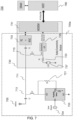
- FIG. 6 illustrates an exemplary block diagram of a SAR sensor implementation 600 according to various examples of the present disclosure.
- the SAR sensor implementation 600 may include an antenna 605, a SAR proximity sensor 603, a radio circuitry 633, a voltage-change detection circuitry 635, and a voltage source 637 electrically connected to each other through one conductive line 611 (e.g., a transmission line). That is, the antenna 605 is connected to the radio circuitry 633 through the conductive line 611.
- the radio circuitry 633 can provide a radio frequency (RF) signal to antenna 605 through the conductive line 611.
- the proximity sensor 603 is also connected to the power source 637 through the same conductive line 611.
- RF radio frequency
- the power source 637 can provide a direct current (DC) voltage supply (e.g., VCC) through the conductive line 611 to power the proximity sensor 603. Additionally, the interrupt port of the sensor 603 is connected to the voltage-change detection circuitry 635 through the same conductive line 611. The sensor 603 can trigger an interrupt and generate an interrupt signal or proximity detection signal by changing the DC voltage level on the conductive line 611. The voltage-change detection circuitry 635 can monitor the DC voltage level (e.g., V OUT ) on the conductive line 611 and detect a voltage change corresponding to the interrupt signal or proximity detection signal.
- DC direct current
- a first end of the conductive line 611 is connected to a first bias tee circuit 613 and a second end of the conductive line 611 is connected to a second bias tee circuit 615.
- the first bias tee circuit 613 electrically connects the antenna 605, the proximity sensor 603, and the conductive line 611 to each other.
- the second bias tee circuit 615 electrically connects the radio circuitry 633, the voltage source 637 and the voltage-change detection circuitry 635, and the conductive line 611 to each other.
- the antenna 605 may be a transmission antenna or a transmission/receiving antenna for over air RF signals.
- the radio circuitry 633 may include a front end circuitry and a radio frequency integrated circuit (RF IC) configured to provide an RF signal via the conductive line 611 to the antenna 605 for transmission over the air.
- the radio circuitry 633 may be connected to a modem or baseband IC.
- the voltage source 637 may be configured to provide a direct current voltage signal (e.g., VCC) via the conductive line 611 to power the proximity sensor 603.
- the proximity sensor 603 may be configured to detect human presence near the antenna 605 and generate an interrupt signal or proximity detection signal when human presence is detected.
- the proximity sensor 603 may be a SAR proximity sensor disposed near the antenna 605.
- the proximity sensor 603 may be configured to provide the interrupt signal (e.g., proximity detection signal) via the conductive line 611.
- the interrupt signal (e.g., proximity detection signal) may be a change in the direct current voltage signal on the conductive line 611.
- the voltage-change detection circuitry 635 may be configured to detect the interrupt signal (e.g., a direct current voltage signal change) on the conductive line 611.
- the radio circuitry 633, the voltage source 637 and voltage-change detection circuitry 635 may be included in a radio/connectivity module 630.
- Each bias tee circuit may include three ports - an RF port, a DC port, and a combined port.
- the bias tee circuit can combine an RF signal (e.g., high frequency voltage changes) on the RF port and a DC signal (e.g., steady or low frequency voltage changes) on the DC port and provide the combined signal on the combined port.
- the bias tee circuit can separate a combined signal (e.g., a multiplexed RF and DC signal including high frequency and low frequency components) to provide an RF signal (e.g., high frequency components) on the RF port and a DC signal (e.g., steady or low frequency components) on the DC port.
- a bias tee circuit may include a capacitor (for DC blocking) and an inductor (for RF decoupling).
- the capacitor acts as a DC block, allowing RF signals to pass.
- the inductor acts as an RF decoupler, allowing DC signals to pass. That is, a bias tee circuit may be a T-shaped junction having an RF port as a first leg, a DC port as a second leg, and a combined port as a third leg.
- the first leg i.e., RF port
- the second leg i.e., DC port
- the third leg i.e., combined port
- the power source 637 may be electrically connected to a DC port of the second bias tee circuit 615
- the radio circuitry 633 may be electrically connected to an RF port of the second bias tee circuit 615
- the conductive line 611 may be electrically connected to the combined port of the second bias tee circuit 615.
- a DC voltage signal provided from the power source 637 may be combined with a radio frequency (RF) signal provided from the radio circuit 633 by means of the second bias tee circuit 615 and the combined RF-DC signal is provided on the conductive line 611.
- RF radio frequency
- the power input port (e.g., VDD pin) of the sensor 603 may be electrically connected to a DC port of the first bias tee circuit 613
- the antenna 605 may be electrically connected to an RF port of the first bias tee circuit 613
- the conductive line 611 may be electrically connected to the combined port of the first bias tee circuit 613.
- the combined RF-DC signal on the conductive line 611 may be separated by means of the first bias tee circuit 613.
- the DC voltage signal provided from the power source 637 may be provided to the DC port of the first bias tee circuit 613 to power the sensor 603.
- the RF signal provided from the radio circuitry 633 may be provided to the RF port of the first bias tee circuit 613 to provide the RF signal to the antenna 605.
- the interrupt port (e.g., NIRQ pin) of sensor 603 may be electrically connected to the DC port of the first bias tee circuit 613 through a resistor 621.
- the interrupt port may be an open drain NIRQ interrupt that pulls the voltage towards ground when activated. That is, during proximity detection, the proximity sensor 603 pulls down the interrupt pin (NIRQ), this pull-down sink current is used to lower the voltage on conductive line 611 by forming a resistor voltage divider.
- the open drain interrupt is connected to the RF path through an inductor and resistor. The inductor is used to isolate the RF from the conductive line 611 and at the same time it will pass DC voltage to/from the sensor.
- the inductor may be part of a bias tee circuit.
- the resistor 621 forms part of the voltage divider and changes the DC voltage level on the conductive line 611. Accordingly, during the proximity detection, the proximity sensor may generate an interrupt that can be detected on the RF path.
- the voltage source 637 may be electrically connected to the DC port through a resistor 623.
- the voltage source 637 and resistors 621 (e.g., R2) and 623 (e.g., R1) may form a resistive divider circuit when an interrupt (e.g., open drain interrupt) is triggered.
- an interrupt e.g., open drain interrupt
- the voltage at a point between resistors 621 (e.g., R2) and 623 (e.g., R1) e.g., conductive line 611, VDD pin of the sensor 603, input to the voltage-change detection circuitry 635) may be considered the output voltage (e.g., V OUT ).
- the output of the resistive divider network e.g., V OUT(proximity) becomes or sets the DC voltage level on the conductive line 611.
- the change in the DC voltage level must remain within a power supply operating range of the sensor 603 (e.g., see Eq. 3).
- the resistor ratio of resistors 621 and 623 may be configured so that the resistive divider circuit provides an output voltage within the operative voltage range of the sensor.
- a SAR proximity sensor 603 may operate in a wide voltage range (e.g., from VDD1 to VDD2). At normal condition (e.g., no human presence in proximity detected, i.e., no interrupt), the proximity sensor 603 operates at a nominal voltage (e.g., 3.3V).
- the power source 637 may provide a direct current voltage signal at the nominal voltage VCC.
- V OUT is approximately VCC.
- the proximity sensor 603 may generate an interrupt signal or proximity indication signal on an open drain output pin (e.g., by pulling the voltage on the pin toward 0V) which results in the formation of a resistor voltage divider with resistors 621 and 623.
- the voltage across the resistor 621 (i.e., R2) between the open drain output pin and the VDD pin of the sensor 603 when proximity is detected may be considered V OUT(proximity) .
- V OUT(proximity) may also be considered as the interrupt signal or proximity indication signal at the voltage-change detection circuit on the radio/connectivity module side by neglecting small current taken by proximity sensor.
- V OUT The DC voltage at a point between the resistors 621 and 623, V OUT , is also the input for powering the sensor 603. That is, V OUT (including V OUT(proximity) and V OUT(no proximity) ) must be within the operating voltage range of the sensor 603. For example, this is reflected in Eq. 3.
- V OUT The DC voltage at a point between the resistors 621 and 623, V OUT , is also the input to the voltage-change detection circuit 635.
- V OUT(no proximity) is approximately the same as VCC and when an interrupt is asserted by the sensor 603 (i.e., human presence detected in proximity of the respective antenna)
- V OUT(proximity) is a fraction of VCC based on the values of resistors 621 (i.e., R2) and 623 (i.e., R1).
- the change in output voltage ( V OUT ) due to the proximity interrupt can be detected by the radio/connectivity module using various detection mechanisms, including, for example, a comparator based implementation or an analog-to-digital converter (ADC) based implementation.
- ADC analog-to-digital converter
- the voltage-change detection circuit 635 may be directly connected to the DC port of the second bias tee circuit 615, so the voltage on the conductive line 611 can be passed to the voltage-change detection circuit 635. Thus, a change in voltage on the conductive line 611 may be detected by the voltage-change detection circuit 635.
- the voltage-change detection circuit 635 in the radio connectivity module 630 may be implemented as a comparator or an ADC.
- the voltage-change detection circuit 635 may be implemented as a comparator or an ADC. The details of the implementation are discussed in greater detail in the examples corresponding to FIGS. 8A , 8B .
- FIG. 7 illustrates an exemplary block diagram of a SAR sensor implementation 700 according to various examples of the present disclosure.
- the SAR sensor implementation 700 may include an antenna 705, a SAR proximity sensor 703, a radio connectivity module 730, a voltage-change detection circuitry 735, and a voltage source 737 electrically connected to each other through one conductive line 711 (e.g., an RF path). That is, the antenna 705 is connected to the radio connectivity module 730 through the conductive line 711.
- the radio connectivity module 730 can provide a radio frequency (RF) signal to antenna 705 through the conductive line 711.
- the proximity sensor 703 is also connected to the power source 737 through the same conductive line 711.
- the power source 737 can provide a direct current voltage supply (e.g., VCC) through the conductive line 711 to power the proximity sensor 703. Additionally, the interrupt port (e.g., pin) of the sensor 703 is connected to the voltage-change detection circuitry 735 through the same conductive line 711. The sensor 703 can trigger an interrupt (i.e., send an interrupt signal) by changing the DC voltage level on the conductive line 711 that can be detected by the voltage-change detection circuitry 735. As shown in FIG. 7 , the sensor 703 does not need to be connected to the host processor device 780.
- the radio connectivity module 730 may include a radio circuitry 733, a baseband IC 731, the voltage-change detection circuit 735, and the power source 737.
- a first end of the conductive line 711 is connected to a first bias tee circuit 713 and a second end of the conductive line 711 is connected to a second bias tee circuit 715.
- the first bias tee circuit 713 electrically connects the antenna 705, the proximity sensor 703, and the conductive line 711 to each other.
- the second bias tee circuit 715 electrically connects the radio circuitry 733, the voltage source 737 and the voltage-change detection circuitry 735, and the conductive line 711 to each other.
- the voltage-change detection circuit 735 may be directly connected to the DC port of the second bias tee circuit 715, so the voltage on the conductive line 711 can be passed to the voltage-change detection circuit 735.
- a change in voltage on the conductive line 711 at the sensor side resulting from the formation of a voltage divider circuit created in response to a pull-down interrupt may be detected on the radio connectivity module side by the voltage-change detection circuit 735.
- the voltage-change detection circuit 735 in the radio connectivity module 730 may be implemented as a comparator or an ADC.
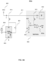
- FIGS. 8A , 8B illustrate exemplary block diagrams of SAR sensor implementations according to various examples of the present disclosure.
- a comparator circuit or an ADC may be used to detect the change in voltage at the radio connectivity module side.
- an in-built ADC is available in a baseband IC chip or modem chip, the in-built ADC can be used for detection OR a comparator may be added.
- Comparator 835a receives as input a reference voltage V REF and a DC voltage on the conductive line (i.e., V OUT ) (e.g., the instantaneous DC voltage on the RF path) and generates as output either a low or high digital logic based on the comparison of V OUT to V REF .
- the V REF may be based on a voltage difference between VCC and V OUT (proximity), where VCC is the nominal voltage provided by the power source and V OUT (proximity) is the DC voltage measured on the conductive line when the sensor interrupt is triggered (e.g., NIRQ pin is pulled-down).
- V REF may be determined based on VCC and V OUT(proximity) according to Eq. 4.
- V REF VCC ⁇ VCC ⁇ V OUT proximity 2
- V OUT is larger than V REF then there is no interrupt signaled by the sensor. If V OUT is less than V REF then there is an interrupt or detection signaled by the sensor.
- One digital logic value e.g., low
- another digital logic value e.g., high
- the baseband IC 731 of the radio connectivity module 830 may use the digital logic to discontinue TX power back off or apply TX power back off based on the predefined values in a look up table (LUT) for the corresponding antenna which reported proximity.
- LUT look up table
- ADC 835b receives as input a DC voltage on the conductive line (i.e., V OUT ) (e.g., the instantaneous DC voltage on the RF path) and generates as output an N-bit digital data value corresponding to the voltage of V OUT .
- the N-bit digital value may be provided to a baseband IC 731.
- the baseband IC 731 may detect a change in voltage by comparing the N-bit ADC output to a predefined value.
- the predefined value may be an N-bit digital value corresponding to an ADC conversion of V REF as defined in Eq. 4. If V OUT is larger than V REF then there is no interrupt signaled by the sensor.
- the baseband IC 731 of the radio connectivity module 830 may discontinue TX power back off or apply TX power back off based on the predefined values in a look up table (LUT) for the corresponding antenna which reported proximity.
- LUT look up table
- comparator or ADC implementations discussed above may also apply to the exemplary SAR implementations 600 and 700.
- the radio connectivity module e.g., modem
- the radio connectivty module 630, 730, 830, 1030 limits the antenna transmission power based on a predefined look up table (LUT) stored in modem software.
- a LUT may include a set of transmission power limits defined by a system designer based on an initial SAR test performed on the system.
- the set of transmission power limits may include a limit per given band and corresponding antenna.
- Table 1 LUT Band Details TX Power limit ANT1 ANT2 ANT3 ANTn B1 14dBm 13dBm 13dBm ...
- the LUT may be implemented as part of a software executed by the modem or baseband IC.
- Antenna ANT1 detects human proximity while operating in band B2, the corresponding TX power limit value may be selected from a LUT table and the new TX power limit may be applied to the corresponding antenna (e.g., ANT1) to control the SAR value.
- the corresponding antenna e.g., ANT1
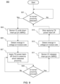
- FIG. 9 illustrates an exemplary flow chart according to examples of the present disclosure.
- the SAR proximity sensor detects if there is human presence in proximity to an antenna. If there is no human presence detected, the sensor continues to monitor.
- the sensor pulls down the interrupt pin (e.g., NIRQ)(sensor side).
- the voltage-change detection circuit detects a change in DC voltage due to the pull down (radio connectivity module side).
- the radio circuitry e.g., RFIC or baseband IC
- applies a transmit power back-off e.g., a new transmit power limit
- the sensor continues to monitor.
- the sensor releases the interrupt pin (e.g., NIRQ)(sensor side).
- the voltage-change detection circuit detects a change in DC voltage due to the release of the pull down (radio connectivity module side).
- the radio circuitry ends the transmission power back-off to the antenna which stopped detecting proximity.
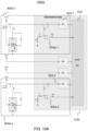
- a SAR sensor array implementation 1000 may include a plurality of SAR implementations 600, 700a, 800a, 800b. That is, the SAR sensor array implementation 1000 may include a radio connectivity module 1030 including a modem or baseband IC 1031 and a SAR implementation 600, 700a, 800a, 800b for each antenna of a multiple antenna system.
- the modem or baseband IC 1031 may include a plurality of general purpose input/output pins or ADC input pins.
- the modem or baseband IC 1031 is configured to receive each proximity detection signal from the respective SAR implementations 600, 700a, 800a, 800b via a respective general purpose input/output pin or a respective ADC input pin.
- the modem or baseband IC 1031 may be connected to the radio circuitry 633, 833, 733.
- the modem or baseband IC 1031 may be configured to independently apply transmission back-off to a respective antenna in response to a respective interrupt/detection signal corresponding to the antenna via a respective radio circuitry 633, 833, 733.
- FIGS. 10A and 10B illustrate exemplary block diagrams of SAR sensor array implementations 1000a, 1000b according to various examples of the present disclosure.
- the SAR sensor array implementation 1000a may include two or more of the implementations of 800a (e.g., 800a-1, 800a-2, ..., 800a-n) connected to a modem or baseband IC 1031.
- 800a e.g., 800a-1, 800a-2, ..., 800a-n
- Each of the radio circuitry 833-1, 833-2, ... 833-n may include front end circuitry or front end and RF circuitry which is connected to the baseband IC 1090.
- the SAR sensor array implementation 1000b may include two or more of the implementations of 800b (e.g., 800b-1, 800b-2, ..., 800b-n) connected to a modem or baseband IC 1090.
- 800b e.g., 800b-1, 800b-2, ..., 800b-n
- the radio circuitry 833-1, 833-2, ... 833-n may include front end circuitry or front end and RF circuitry which is connected to the baseband IC 1090.
- a SAR sensor array implementation 1000 may similarly include two or more of the implementations of 600 or 700. Accordingly, the SAR sensor array implementations disclosed herein are not constrained by the number of interrupt ports of a baseband IC.
- the advantages of this implementation include no dependence on the host system or the host software for SAR implementation; no additional cable, traces and flexible printed circuit boards (FPCs) for proximity sensor supply and interrupt (less design complexity); the power back-off can be applied only for the antenna(s) which detected proximity, instead complete back-off (i.e., back-off on all antennas). Proximity detection and power back-off can be applied even during abnormal platform states such as OS crash or system hang, as the proposed implementation is independent of the host (SOC).
- the proposed implementation is scalable for multiple transmit antenna configurations. It can also be extended to multiple radio modules (e.g., WWAN and WLAN).
- the proximity and power back-off can be functional when the connected modem is in Standby mode as well.
- Example D1 may include a communication device including: an antenna; a proximity sensor configured to detect human presence near the antenna and generate an interrupt signal when human presence is detected; a radio frequency (RF) circuitry configured to provide an RF signal via a transmission line to the antenna for transmission over the air; a voltage source configured to provide a power supply voltage to the proximity sensor; and a voltage-change detection circuitry configured to detect the interrupt signal; a first bias tee circuit electrically connecting the antenna, the proximity sensor, and the transmission line to each other; a second bias tee circuit electrically connecting the RF circuitry, the voltage source, the voltage-change detection circuitry, and the transmission line to each other; and a modem circuitry configured to determine a transmission power of the antenna based on the whether the interrupt signal is detected, the modem circuitry electrically connected to the RF circuitry.
- RF radio frequency
- Example D1.1 may include the device of Example D1 and/or some other example herein, wherein the proximity sensor is electrically connected to the first bias tee circuit through a first resistor, the voltage source is electrically connected to the second bias tee circuit through a second resistor, voltage-change detection circuitry is electrically connected to a point between the second resistor and the second bias tee circuit,
- Example D1.2 may include the device of Example D1 and/or some other example herein, wherein the interrupt signal is a proximity indication signal having a voltage corresponding to a fraction of the power supply voltage, the fraction being a ratio based on the first and second resistors.
- the interrupt signal is a proximity indication signal having a voltage corresponding to a fraction of the power supply voltage, the fraction being a ratio based on the first and second resistors.
- Example D2 may include the device of Example D1 and/or some other example herein, wherein each of the first and second bias tee circuits includes a first port configured to pass voltage biasing signals, a second port configured to pass radio-frequency signals, and a combined port configured to pass both the voltage biasing signals and radio-frequency signals.
- Example D3 may include the device of Example D2 and/or some other example herein, wherein the antenna is electrically connected to the second port of the first bias tee circuit, the proximity sensor is electrically connected to the first port of the first bias tee circuit, and a first end of the transmission line is electrically connected to the combined port of the first bias tee circuit, and wherein the RF circuitry is electrically connected to the second port of the second bias tee circuit, the voltage source and the voltage-change detection circuitry are electrically connected to the first port of the second bias tee circuit, and a second end of the transmission line is electrically coupled to the combined port of the second bias tee circuit.
- Example D4 may include the device of Example D3 and/or some other example herein, wherein the proximity sensor includes a power port and an interrupt port, the power port is electrically connected to the first port of the first bias tee circuit and the interrupt port is electrically connected to the power port and the first port of the first bias tee circuit through a first resistor, wherein the RF circuitry includes an antenna port electrically connected to the second port of the second bias tee circuit, wherein the voltage source is electrically connected to the first port of the second bias tee circuit through a second resistor, and wherein the voltage-change detection circuitry includes a voltage input port electrically coupled to the first port of the second bias tee circuit.
- Example D5 may include the device of Example 4 and/or some other example herein, wherein the first and second resistors comprise a resistor voltage divider circuit.
- Example D6 may include the device of Example D5 and/or some other example herein, wherein the proximity sensor is configured to operate within a range of power supply voltages, and wherein the interrupt port is configured as an open drain interrupt, and wherein the resistor voltage divider circuit is configured to provide a power voltage within the range of power supply voltages.
- Example D6.1 may include the device of Example D6 and/or some other example herein, wherein the power voltage is the power supply voltage when the interrupt signal is not generated and the power voltage is a fraction of the power supply voltage when the interrupt signal is generated.
- Example D7 may include the device of any of Examples D1-D6 and/or some other example herein, wherein the first port of the first and second bias tee circuits is a low-frequency port and the second port of the first and second bias tee circuits is a high-frequency port.
- Example D8 may include the device of any of Examples D1-D7 and/or some other example herein, wherein the voltage-change detection circuitry includes a voltage comparator circuitry.
- Example D9 may include the device of D8 and/or some other example herein, wherein the voltage-change detection circuitry includes a second voltage input port configured to receive a reference voltage and an output port configured to provide a digital signal to the modem circuitry, wherein the voltage comparator circuitry is configured to compare a voltage at the voltage input port to the reference voltage and generate a digital logic output at the output port, wherein the digital logic output indicates whether the interrupt signal is detected.
- the voltage-change detection circuitry includes a second voltage input port configured to receive a reference voltage and an output port configured to provide a digital signal to the modem circuitry
- the voltage comparator circuitry is configured to compare a voltage at the voltage input port to the reference voltage and generate a digital logic output at the output port, wherein the digital logic output indicates whether the interrupt signal is detected.
- Example D10 may include the device of any of Examples D1-D7 and/or some other example herein, wherein the voltage-change detection circuitry comprises an analog-to-digital converter (ADC) circuitry included in the modem circuitry.
- ADC analog-to-digital converter
- Example D11 may include the device of Example D10 and/or some other example herein, wherein the ADC circuitry converts a voltage at the first port of the second bias tee circuit to a digital value and the voltage-change detection circuitry compares the digital value to a predetermined threshold value and generates an output that indicates whether the interrupt signal is detected.
- Example D12 may include the device of any of Examples D1-D11 and/or some other example herein, wherein the modem circuitry is configured to determine the transmission power based on predefined values in a look up table corresponding to the antenna.
- Example D13 may include the device of any of Examples D1-D12 and/or some other example herein, wherein the first port of the first and second bias tee circuits includes an inductor, the second port of the first and second bias tee circuits includes a capacitor, and the combined port of the first and second bias tee circuits includes a point between the inductor and the capacitor.
- Example D14 may include the device of any of Examples D1-D13 and/or some other example herein, wherein the proximity sensor is a SAR sensor.
- Example D15 may include the device of any of Examples D1-D14 and/or some other example herein, further comprising: a second antenna; a second proximity sensor configured to detect human presence near the second antenna and generate a second interrupt signal when human presence is detected; a second radio frequency (RF) circuitry configured to provide a second RF signal via a second transmission line to the second antenna for transmission over the air; a second voltage source configured to provide a power supply voltage to the second proximity sensor; and a second voltage-change detection circuitry configured to detect the second interrupt signal; a third bias tee circuit electrically connecting the second antenna, the second proximity sensor, and the second transmission line to each other; and a fourth bias tee circuit electrically connecting the second RF circuitry, the second voltage source, the second voltage-change detection circuitry, and the second transmission line to each other, wherein the first voltage-change detection circuitry is a comparator circuit connected to the modem circuit through a general purpose pin or the first voltage-change detection circuitry is an analog-to-digital converter of the
- implementations of methods detailed herein are exemplary in nature, and are thus understood as capable of being implemented in a corresponding device.
- implementations of devices detailed herein are understood as capable of being implemented as a corresponding method. It is thus understood that a device corresponding to a method detailed herein may include one or more components configured to perform each aspect of the related method.
Landscapes
- Engineering & Computer Science (AREA)
- Computer Networks & Wireless Communication (AREA)
- Theoretical Computer Science (AREA)
- Signal Processing (AREA)
- Physics & Mathematics (AREA)
- General Engineering & Computer Science (AREA)
- General Physics & Mathematics (AREA)
- Mobile Radio Communication Systems (AREA)
Abstract
Description
- Various aspects generally relating to transmit power control for regulating radiation exposure in wireless communications.
- New communication technologies, such as 5G New Radio (NR), WiGig, and Wireless Local Area Networks (WLANs) such as WiFi, utilize higher radio frequencies in the millimeter wave (mmWave) spectrum and utilize beamforming to improve throughput and reduce frequency with existing wireless systems. While these techniques provide many advantages in these newer wireless systems, they may increase radio frequency (RF) radiation in the environment, including to users. For example, when a device uses beamforming to focus high RF transmissions in a narrow direction, the resulting beam may deliver elevated levels of radiation energy to a focused area. When this focused area is pointed at a user, the device may deliver high levels of harmful radiation to the user and the signal quality may also be significantly degraded. The amount of radiation energy emitted absorbed by a unit of mass of a user over time may be defined as the specific absorption rate (SAR).
- Various regulators, including the Federal Communications Commission (FCC) and the International Commission on Non-Ionizing Radiation Protection (ICNIRP), and standardization bodies like the 3rd Generation Partnership Project (3GPP) have introduced SAR measures that limit the amount of radiation that a device can deliver to users. In response, methods and devices that implement SAR proximity sensors to detect human presence and to reduce antenna transmission power when human presence is detected near antennas have been introduced to comply with these regulatory measures.
- In the drawings, like reference characters generally refer to the same parts throughout the different views. The drawings are not necessarily to scale, emphasis instead generally being placed upon illustrating the principles of the disclosure. In the following description, various aspects of the disclosure are described with reference to the following drawings, in which:
-
FIG. 1 exemplarily shows a radio communication network according to some aspects; -
FIG. 2 exemplarily shows an internal configuration of terminal device according to some aspects; -
FIG. 3 exemplarily shows an internal configuration of a network access node in some aspects; -
FIG. 4 exemplarily illustrates a block diagram of an existing SAR proximity sensor implementation; -
FIG. 5 exemplarily illustrates a block diagram of an existing SAR proximity sensor implementation; -
FIG. 6 exemplarily illustrates a block diagram of a SAR sensor implementation according to various examples of the present disclosure; -
FIG. 7 exemplarily illustrates a block diagram of a SAR sensor implementation according to various examples of the present disclosure; -
FIGS. 8A ,8B exemplarily illustrate block diagrams of SAR sensor implementations according to various examples of the present disclosure; -
FIG. 9 exemplarily illustrates a flowchart according to various examples of the present disclosure; and -
FIGS. 10A ,10B exemplarily illustrate block diagrams of SAR sensor array implementations according to various examples of the present disclosure. - Current radio systems come with multiple antenna configurations ranging from 2 to 8 or more antennas to support the multi-transmission scenarios like ULCA, ENDC & UL-MIMO configuration. To comply with SAR regulations, dynamic power reduction is required when a human body comes in proximity with the transmitting antenna. In multiple transmit antenna systems, each antenna needs a dedicated power control to comply with regulatory in the event of human proximity. This calls for multiple interrupt signals to be communicated to the radio/connectivity module from the sensor hub or host SoC. However, typical radio/connectivity modules follow an M.2 standard, which only requires a single interrupt pin for SAR detection (e.g., a single DPR pin). Due to this, assigning additional interrupt lines will be a major design challenge.
- Existing SAR proximity sensor implementations can detect human presence and reduce antenna transmission power when human presence is detected near antennas but have various disadvantages. For example, in some existing SAR proximity sensor implementations, when the SAR proximity sensor detects human presence, the SAR proximity sensor is configured to send an interrupt to a host processor device (e.g., system-on-a-chip (SoC). In such implementations, the host processor device plays a significant role in processing and handling interrupts from the SAR proximity sensor. In some other existing SAR proximity implemenations, when the SAR proximity sensor detects human presence, the SAR proximity sensor is configured to send an interrupt to a modem. In such implementations, it is very complicated to provide individual antenna power management in a multiple antenna system.
-
FIG. 4 illustrates an exemplary block diagram of an existing SARproximity sensor implementation 400. Referring toFIG. 4 ,antennas SAR proximity sensor 403 includesproximity sensing electrodes antennas host processor device 480 connected to theproximity sensor 403 and theradio connectivity module 490. Thehost processor device 480 may include aninterface hub 483 for communicating with theradio connectivity module 490 and theproximity sensor 403. Theinterface hub 483 may include a sensor hub 481 (e.g., a microcontroller unit/coprocessor/DSP) for receiving and processing data from theproximity sensor 403. -
FIG. 5 illustrates an exemplary block diagram of an existing SAR proximity sensor implementation 500. Referring toFIG. 5 ,antenna 505 is electrically connected to aradio connectivity module 590, aSAR proximity sensor 503 includesproximity sensing electrode 504 disposed nearantenna 505, and ahost processor device 580 connected to theradio connectivity module 590. Theradio connectivity module 590 may include front-end andRF IC module 591 and abaseband IC module 593. Thehost processor device 580 may also be connected to thesensor 503. Thehost processor device 580 may include an interface hub for communicating with theradio connectivity module 590 and theproximity sensor 503. For example, an interrupt pin (e.g., DPR pin) of the modem may be asserted by the host processor device 580 (e.g., SoC) or directly by the SAR sensor. - In some existing configurations, the
proximity sensor host processor device proximity sensor interface hub 483 of thehost processor device host processor device sensor host processor device radio connectivity module - In some other existing implementations, the
proximity sensor modem proximity sensor radio connectivity module 490, 590 (e.g., via a DPR pin). That is, the interrupt is not transmitted to thehost processor device - The disadvantages of current SAR implementations include higher system complexity as the proximity sensor interrupt is connected to the radio module through a sensor hub or from the host processor. In a case when the proximity sensor interrupt is indirectly asserted to the radio/connectivity module, there is software overhead from the system platform standpoint because the host processor device is involved in the interrupt handling process. In a case when the proximity sensor interrupt is directly asserted to the radio/connectivity module, multiple interrupt ports at the radio module would be required to support independent antenna power management in a multiple antenna transmission scenario. In a case of a single interrupt port (e.g. DPR pin) implementation, the existing solution cannot distinguish among multiple antenna transmit scenarios and the power back off will be applied to all antennas irrespective of which antenna/antennae detected the proximity.
- The present disclosure provides an innovative way to power the SAR proximity sensor and communicate the sensor interrupt back to the radio/connectivity module using an antenna interconnect (e.g., a connection line between the radio connectivity module and the antenna, i.e., an RF path). In this manner, the proximity detection/interrupt can be communicated to a radio/connectivity module without using or adding additional interconnect pins on the radio/connectivity module interface and without involving the host system. The methods and devices provided herein are better able to regulate antenna transmission power and provide numerous advantages in wireless communications systems.
- In some aspects, methods and devices are configured to use a single line for transmitting an RF signal to an antenna, powering a proximity sensor, and communicating an interrupt condition from the proximity sensor to the radio/connectivity module. The methods and devices provide that the SAR sensor is connected via a bias tee port. The methods and devices of this disclosure provide numerous advantages, including (but not limited to): eliminating involvement of the host processor; simplifying routing and interconnect design; allowing individual power management for multiple antennas.
- The following detailed description refers to the accompanying drawings that show, by way of illustration, specific details and aspects in which the disclosure may be practiced.
- The word "exemplary" is used herein to mean "serving as an example, instance, or illustration". Any aspect or design described herein as "exemplary" is not necessarily to be construed as preferred or advantageous over other aspects or designs.
- The words "plurality" and "multiple" in the description or the claims expressly refer to a quantity greater than one. The terms "group (of)", "set [of]", "collection (of)", "series (of)", "sequence (of)", "grouping (of)", etc., and the like in the description or in the claims refer to a quantity equal to or greater than one, i.e. one or more. Any term expressed in plural form that does not expressly state "plurality" or "multiple" likewise refers to a quantity equal to or greater than one. The terms "proper subset", "reduced subset", and "lesser subset" refer to a subset of a set that is not equal to the set, i.e. a subset of a set that contains less elements than the set.
- Any vector and/or matrix notation utilized herein is exemplary in nature and is employed solely for purposes of explanation. Accordingly, aspects of this disclosure accompanied by vector and/or matrix notation are not limited to being implemented solely using vectors and/or matrices, and that the associated processes and computations may be equivalently performed with respect to sets, sequences, groups, etc., of data, observations, information, signals, samples, symbols, elements, etc.
- As used herein, "memory" is understood as a non-transitory computer-readable medium in which data or information can be stored for retrieval. References to "memory" included herein may thus be understood as referring to volatile or non-volatile memory, including random access memory (RAM), read-only memory (ROM), flash memory, solid-state storage, magnetic tape, hard disk drive, optical drive, etc., or any combination thereof. Furthermore, registers, shift registers, processor registers, data buffers, etc., are also embraced herein by the term memory. A single component referred to as "memory" or "a memory" may be composed of more than one different type of memory, and thus may refer to a collective component including one or more types of memory. Any single memory component may be separated into multiple collectively equivalent memory components, and vice versa. Furthermore, while memory may be depicted as separate from one or more other components (such as in the drawings), memory may also be integrated with other components, such as on a common integrated chip or a controller with an embedded memory.
- The term "software" refers to any type of executable instruction, including firmware.
- The term "terminal device" utilized herein refers to user-side devices (both portable and fixed) that can connect to a core network and/or external data networks via a radio access network. "Terminal device" can include any mobile or immobile wireless communication device, including User Equipment (UEs), Mobile Stations (MSs), Stations (STAs), cellular phones, tablets, laptops, personal computers, wearables, multimedia playback and other handheld or body-mounted electronic devices, consumer/home/office/commercial appliances, vehicles, and any other electronic device capable of user-side wireless communications. Without loss of generality, in some cases terminal devices can also include application-layer components, such as application processors or other general processing components that are directed to functionality other than wireless communications. Terminal devices can optionally support wired communications in addition to wireless communications. Furthermore, terminal devices can include vehicular communication devices that function as terminal devices.
- The term "network access node" as utilized herein refers to a network-side device that provides a radio access network with which terminal devices can connect and exchange information with a core network and/or external data networks through the network access node. "Network access nodes" can include any type of base station or access point, including macro base stations, micro base stations, NodeBs, evolved NodeBs (eNBs), Home base stations, Remote Radio Heads (RRHs), relay points, Wireless Local Area Network (WLAN) Access Points (APs), Bluetooth master devices, DSRC RSUs, terminal devices acting as network access nodes, and any other electronic device capable of network-side wireless communications, including both immobile and mobile devices (e.g., vehicular network access nodes, moving cells, and other movable network access nodes). As used herein, a "cell" in the context of telecommunications may be understood as a sector served by a network access node. Accordingly, a cell may be a set of geographically co-located antennas that correspond to a particular sectorization of a network access node. A network access node can thus serve one or more cells (or sectors), where the cells are characterized by distinct communication channels. Furthermore, the term "cell" may be utilized to refer to any of a macrocell, microcell, femtocell, picocell, etc. Certain communication devices can act as both terminal devices and network access nodes, such as a terminal device that provides network connectivity for other terminal devices.
- Various aspects of this disclosure may utilize or be related to radio communication technologies. While some examples may refer to specific radio communication technologies, the examples provided herein may be similarly applied to various other radio communication technologies, both existing and not yet formulated, particularly in cases where such radio communication technologies share similar features as disclosed regarding the following examples. As used herein, a first radio communication technology may be different from a second radio communication technology if the first and second radio communication technologies are based on different communication standards.
- Aspects described herein may use such radio communication technologies according to various spectrum management schemes, including, but not limited to, dedicated licensed spectrum, unlicensed spectrum, (licensed) shared spectrum (such as LSA, "Licensed Shared Access," in 2.3-2.4 GHz, 3.4-3.6 GHz, 3.6-3.8 GHz and further frequencies and SAS, "Spectrum Access System," in 3.55-3.7 GHz and further frequencies)., and may be use various spectrum bands including, but not limited to, IMT (International Mobile Telecommunications) spectrum (including 450 - 470 MHz, 790 - 960 MHz, 1710 - 2025 MHz, 2110 - 2200 MHz, 2300 - 2400 MHz, 2500 - 2690 MHz, 698-790 MHz, 610 - 790 MHz, 3400 - 3600 MHz, etc., where some bands may be limited to specific region(s) and/or countries), IMT-advanced spectrum, IMT-2020 spectrum (expected to include 3600-3800 MHz, 3.5 GHz bands, 700 MHz bands, bands within the 24.25-86 GHz range, etc.), spectrum made available under FCC's "Spectrum Frontier" 5G initiative (including 27.5 - 28.35 GHz, 29.1 - 29.25 GHz, 31 - 31.3 GHz, 37 - 38.6 GHz, 38.6 - 40 GHz, 42 - 42.5 GHz, 57 - 64 GHz, 64 - 71 GHz, 71 - 76 GHz, 81 - 86 GHz and 92 - 94 GHz, etc.), the ITS (Intelligent Transport Systems) band of 5.9 GHz (typically 5.85-5.925 GHz) and 63-64 GHz, bands currently allocated to WiGig such as WiGig Band 1 (57.24-59.40 GHz), WiGig Band 2 (59.40-61.56 GHz) and WiGig Band 3 (61.56-63.72 GHz) and WiGig Band 4 (63.72-65.88 GHz), the 70.2 GHz - 71 GHz band, any band between 65.88 GHz and 71 GHz, bands currently allocated to automotive radar applications such as 76-81 GHz, and future bands including 94-300 GHz and above.
- For purposes of this disclosure, radio communication technologies may be classified as one of a Short-Range radio communication technology or Cellular Wide Area radio communication technology. Short Range radio communication technologies may include Bluetooth, WLAN (e.g., according to any IEEE 802.11 standard), and other similar radio communication technologies. Cellular Wide Area radio communication technologies may include Global System for Mobile Communications (GSM), Code Division Multiple Access 2000 (CDMA2000), Universal Mobile Telecommunications System (UMTS), Long Term Evolution (LTE), General Packet Radio Service (GPRS), Evolution-Data Optimized (EV-DO), Enhanced Data Rates for GSM Evolution (EDGE), High Speed Packet Access (HSPA; including High Speed Downlink Packet Access (HSDPA), High Speed Uplink Packet Access (HSUPA), HSDPA Plus (HSDPA+), and HSUPA Plus (HSUPA+)), Worldwide Interoperability for Microwave Access (WiMax) (e.g., according to an IEEE 802.16 radio communication standard, e.g., WiMax fixed or WiMax mobile), etc., and other similar radio communication technologies. Cellular Wide Area radio communication technologies also include "small cells" of such technologies, such as microcells, femtocells, and picocells. Cellular Wide Area radio communication technologies may be generally referred to herein as "cellular" communication technologies.
- The terms "radio communication network," "wireless network", "communication network," or the like, as utilized herein encompasses both an access section of a network (e.g., a radio access network (RAN) section) and a core section of a network (e.g., a core network section). The term "radio idle mode" or "radio idle state" used herein in reference to a terminal device refers to a radio control state in which the terminal device is not allocated at least one dedicated communication channel of a mobile communication network. The term "radio connected mode" or "radio connected state" used in reference to a terminal device refers to a radio control state in which the terminal device is allocated at least one dedicated uplink communication channel of a radio communication network.
- Unless explicitly specified, the term "transmit" encompasses both direct (point-to-point) and indirect transmission (via one or more intermediary points). Similarly, the term "receive" encompasses both direct and indirect reception. Furthermore, the terms "transmit", "receive", "communicate", and other similar terms encompass both physical transmission (e.g., the transmission of radio signals) and logical transmission (e.g., the transmission of digital data over a logical software-level connection). For example, a processor or controller may transmit or receive data over a software-level connection with another processor or controller in the form of radio signals, where the physical transmission and reception is handled by radio-layer components such as RF transceivers and antennas, and the logical transmission and reception over the software-level connection is performed by the processors or controllers. The term "communicate" may encompass one or both of transmitting and receiving, i.e., unidirectional or bidirectional communication in one or both of the incoming and outgoing directions. The term "calculate" may encompass both 'direct' calculations via a mathematical expression/formula/relationship and 'indirect' calculations via lookup or hash tables and other array indexing or searching operations.
-
FIGs. 1 and2 depict an exemplary network and device architecture for wireless communications. In particular,FIG. 1 shows exemplaryradio communication network 100 according to some aspects, which may includeterminal devices network access nodes Radio communication network 100 may communicate withterminal devices network access nodes radio communication network 100 is exemplary and is scalable to any amount. - In an exemplary cellular context,
network access nodes terminal devices Network access nodes radio communication network 100. The cellular core network may interface with one or more external data networks. In an exemplary short-range context,network access node terminal device Network access nodes -
Network access nodes 110 and 120 (and, optionally, other network access nodes ofradio communication network 100 not explicitly shown inFIG. 1 ) may accordingly provide a radio access network toterminal devices 102 and 104 (and, optionally, other terminal devices ofradio communication network 100 not explicitly shown inFIG. 1 ). In an exemplary cellular context, the radio access network provided bynetwork access nodes terminal devices terminal devices radio communication network 100, etc.) and external data networks (e.g., data networks providing voice, text, multimedia (audio, video, image), and other Internet and application data). In an exemplary short-range context, the radio access network provided bynetwork access nodes - The radio access network and core network (if applicable, such as for a cellular context) of
radio communication network 100 may be governed by communication protocols that can vary depending on the specifics ofradio communication network 100. Such communication protocols may define the scheduling, formatting, and routing of both user and control data traffic throughradio communication network 100, which includes the transmission and reception of such data through both the radio access and core network domains ofradio communication network 100. Accordingly,terminal devices network access nodes radio communication network 100, while the core network may follow the defined communication protocols to route data within and outside of the core network. Exemplary communication protocols include LTE, UMTS, GSM, WiMAX, Bluetooth, WLAN, mmWave, etc., any of which may be applicable toradio communication network 100. - As shown in
radio communication network 100,terminal device 102 andnetwork access node 110 may each usebeamforming techniques network 100 may be capable of bidirectional beamforming. If a user is in the direction of thebeam 102b, for example, the user may be subject to increased SAR levels. In order to comply with regulatory measures,terminal device 102 may need to implement TAS mechanisms so that the amount of energy transmitted in the direction of the user does not violate (i.e., go over) a TAS energy budget for a given period of time. However, in addition to complying with these regulatory measures,terminal device 102 must also attempt to maintain a robust wireless link withnetwork access node 110 to ensure communication quality is not degraded. -
FIG. 2 shows an internal configuration ofterminal device 102 according to some aspects, which may includeantenna system 202, radio frequency (RF)transceiver 204, baseband modem 206 (includingdigital signal processor 208 and protocol controller 210),application processor 212, andmemory 214. Although not explicitly shown inFIG. 2 , in some aspectsterminal device 102 may include one or more additional hardware and/or software components, such as processors/microprocessors, controllers/microcontrollers, other specialty or generic hardware/processors/circuits, peripheral device(s), memory, power supply, external device interface(s), subscriber identity module(s) (SIMs), user input/output devices (display(s), keypad(s), touchscreen(s), speaker(s), external button(s), camera(s), microphone(s), etc.), or other related components. -
Terminal device 102 may transmit and receive radio signals on one or more radio access networks.Baseband modem 206 may direct such communication functionality ofterminal device 102 according to the communication protocols associated with each radio access network, and may execute control overantenna system 202 andRF transceiver 204 to transmit and receive radio signals according to the formatting and scheduling parameters defined by each communication protocol. Although various practical designs may include separate communication components for each supported radio communication technology (e.g., a separate antenna, RF transceiver, digital signal processor, and controller), for purposes of conciseness the configuration ofterminal device 102 shown inFIG. 2 depicts only a single instance of such components. -
Terminal device 102 may transmit and receive wireless signals withantenna system 202, which may be a single antenna or an antenna array that includes multiple antennas. In some aspects,antenna system 202 may additionally include analog antenna combination and/or beamforming circuitry. In the receive (RX) path,RF transceiver 204 may receive analog radio frequency signals fromantenna system 202 and perform analog and digital RF front-end processing on the analog radio frequency signals to produce digital baseband samples (e.g., In-Phase/Quadrature (IQ) samples) to provide tobaseband modem 206.RF transceiver 204 may include analog and digital reception components including amplifiers (e.g., Low Noise Amplifiers (LNAs)), filters, RF demodulators (e.g., RF IQ demodulators)), and analog-to-digital converters (ADCs), whichRF transceiver 204 may utilize to convert the received radio frequency signals to digital baseband samples. In the transmit (TX) path,RF transceiver 204 may receive digital baseband samples frombaseband modem 206 and perform analog and digital RF front-end processing on the digital baseband samples to produce analog radio frequency signals to provide toantenna system 202 for wireless transmission.RF transceiver 204 may thus include analog and digital transmission components including amplifiers (e.g., Power Amplifiers (PAs), filters, RF modulators (e.g., RF IQ modulators), and digital-to-analog converters (DACs), whichRF transceiver 204 may utilize to mix the digital baseband samples received frombaseband modem 206 and produce the analog radio frequency signals for wireless transmission byantenna system 202. In someaspects baseband modem 206 may control the radio transmission and reception ofRF transceiver 204, including specifying the transmit and receive radio frequencies for operation ofRF transceiver 204. - As shown in
FIG. 2 ,baseband modem 206 may includedigital signal processor 208, which may perform physical layer (PHY, Layer 1) transmission and reception processing to, in the transmit path, prepare outgoing transmit data provided byprotocol controller 210 for transmission viaRF transceiver 204, and, in the receive path, prepare incoming received data provided byRF transceiver 204 for processing byprotocol controller 210.Digital signal processor 208 may be configured to perform one or more of error detection, forward error correction encoding/decoding, channel coding and interleaving, channel modulation/demodulation, physical channel mapping, radio measurement and search, frequency and time synchronization, antenna diversity processing, power control and weighting, rate matching/de-matching, retransmission processing, interference cancelation, and any other physical layer processing functions.Digital signal processor 208 may be structurally realized as hardware components (e.g., as one or more digitally-configured hardware circuits or FPGAs), software-defined components (e.g., one or more processors configured to execute program code defining arithmetic, control, and I/O instructions (e.g., software and/or firmware) stored in a non-transitory computer-readable storage medium), or as a combination of hardware and software components. In some aspects,digital signal processor 208 may include one or more processors configured to retrieve and execute program code that defines control and processing logic for physical layer processing operations. In some aspects,digital signal processor 208 may execute processing functions with software via the execution of executable instructions. In some aspects,digital signal processor 208 may include one or more dedicated hardware circuits (e.g., ASICs, FPGAs, and other hardware) that are digitally configured to specific execute processing functions, where the one or more processors ofdigital signal processor 208 may offload certain processing tasks to these dedicated hardware circuits, which are known as hardware accelerators. Exemplary hardware accelerators can include Fast Fourier Transform (FFT) circuits and encoder/decoder circuits. In some aspects, the processor and hardware accelerator components ofdigital signal processor 208 may be realized as a coupled integrated circuit. -
Terminal device 102 may be configured to operate according to one or more radio communication technologies.Digital signal processor 208 may be responsible for lower-layer processing functions (e.g.,Layer 1/PHY) of the radio communication technologies, whileprotocol controller 210 may be responsible for upper-layer protocol stack functions (e.g., Data Link Layer/Layer 2 and/or Network Layer/Layer 3).Protocol controller 210 may thus be responsible for controlling the radio communication components of terminal device 102 (antenna system 202,RF transceiver 204, and digital signal processor 208) in accordance with the communication protocols of each supported radio communication technology, and accordingly may represent the Access Stratum and Non-Access Stratum (NAS) (also encompassingLayer 2 and Layer 3) of each supported radio communication technology.Protocol controller 210 may be structurally embodied as a processor configured to execute protocol stack software (retrieved from a controller memory) and subsequently control the radio communication components ofterminal device 102 to transmit and receive communication signals in accordance with the corresponding protocol stack control logic defined in the protocol stack software.Protocol controller 210 may include one or more processors configured to retrieve and execute program code that defines the upper-layer protocol stack logic for one or more radio communication technologies, which can include Data Link Layer/Layer 2 and Network Layer/Layer 3 functions.Protocol controller 210 may be configured to perform both user-plane and control-plane functions to facilitate the transfer of application layer data to and fromradio terminal device 102 according to the specific protocols of the supported radio communication technology. User-plane functions can include header compression and encapsulation, security, error checking and correction, channel multiplexing, scheduling and priority, while control-plane functions may include setup and maintenance of radio bearers. The program code retrieved and executed byprotocol controller 210 may include executable instructions that define the logic of such functions. - In some aspects,
terminal device 102 may be configured to transmit and receive data according to multiple radio communication technologies. Accordingly, in some aspects one or more ofantenna system 202,RF transceiver 204,digital signal processor 208, andprotocol controller 210 may include separate components or instances dedicated to different radio communication technologies and/or unified components that are shared between different radio communication technologies. For example, in someaspects protocol controller 210 may be configured to execute multiple protocol stacks, each dedicated to a different radio communication technology and either at the same processor or different processors. In some aspects,digital signal processor 208 may include separate processors and/or hardware accelerators that are dedicated to different respective radio communication technologies, and/or one or more processors and/or hardware accelerators that are shared between multiple radio communication technologies. In some aspects,RF transceiver 204 may include separate RF circuitry sections dedicated to different respective radio communication technologies, and/or RF circuitry sections shared between multiple radio communication technologies. In some aspects,antenna system 202 may include separate antennas dedicated to different respective radio communication technologies, and/or antennas shared between multiple radio communication technologies. Accordingly, whileantenna system 202,RF transceiver 204,digital signal processor 208, andprotocol controller 210 are shown as individual components inFIG. 2 , in someaspects antenna system 202,RF transceiver 204,digital signal processor 208, and/orprotocol controller 210 may encompass separate components dedicated to different radio communication technologies. - The
terminal device 102 may also includeapplication processor 212 andmemory 214.Application processor 212 may be a CPU, and may be configured to handle the layers above the protocol stack, including the transport and application layers.Application processor 212 may be configured to execute various applications and/or programs ofterminal device 102 at an application layer ofterminal device 102, such as an operating system (OS), a user interface (UI) for supporting user interaction withterminal device 102, and/or various user applications. The application processor may interface withbaseband modem 206 and act as a source (in the transmit path) and a sink (in the receive path) for user data, such as voice data, audio/video/image data, messaging data, application data, basic Internet/web access data, etc. In the transmit path,protocol controller 210 may therefore receive and process outgoing data provided byapplication processor 212 according to the layer-specific functions of the protocol stack, and provide the resulting data todigital signal processor 208.Digital signal processor 208 may then perform physical layer processing on the received data to produce digital baseband samples, which digital signal processor may provide toRF transceiver 204.RF transceiver 204 may then process the digital baseband samples to convert the digital baseband samples to analog RF signals, whichRF transceiver 204 may wirelessly transmit viaantenna system 202. In the receive path,RF transceiver 204 may receive analog RF signals fromantenna system 202 and process the analog RF signals to obtain digital baseband samples.RF transceiver 204 may provide the digital baseband samples todigital signal processor 208, which may perform physical layer processing on the digital baseband samples.Digital signal processor 208 may then provide the resulting data toprotocol controller 210, which may process the resulting data according to the layer-specific functions of the protocol stack and provide the resulting incoming data toapplication processor 212.Application processor 212 may then handle the incoming data at the application layer, which can include execution of one or more application programs with the data and/or presentation of the data to a user via a user interface. -
Memory 214 may embody a memory component ofterminal device 102, such as a hard drive or another such permanent memory device. Although not explicitly depicted inFIG. 2 , the various other components ofterminal device 102 shown inFIG. 2 may additionally each include integrated permanent and non-permanent memory components, such as for storing software program code, buffering data, etc. - In accordance with some radio communication networks,
terminal devices radio communication network 100. As each network access node ofradio communication network 100 may have a specific coverage area,terminal devices radio communication network 100. For example,terminal device 102 may establish a radio access connection withnetwork access node 110 whileterminal device 104 may establish a radio access connection withnetwork access node 120. In the event that the current radio access connection degrades,terminal devices radio communication network 100; for example,terminal device 104 may move from the coverage area ofnetwork access node 120 into the coverage area ofnetwork access node 110. As a result, the radio access connection withnetwork access node 120 may degrade, whichterminal device 104 may detect via radio measurements such as signal strength or signal quality measurements ofnetwork access node 120. -
FIG. 3 shows an exemplary internal configuration of a network access node, such asnetwork access node 110, according to some aspects. As shown inFIG. 3 ,network access node 110 may includeantenna system 302,radio transceiver 304, and baseband subsystem 306 (includingphysical layer processor 308 and protocol controller 310). In an abridged overview of the operation ofnetwork access node 110,network access node 110 may transmit and receive wireless signals viaantenna system 302, which may be an antenna array including multiple antennas.Radio transceiver 304 may perform transmit and receive RF processing to convert outgoing baseband samples frombaseband subsystem 306 into analog radio signals to provide toantenna system 302 for radio transmission and to convert incoming analog radio signals received fromantenna system 302 into baseband samples to provide tobaseband subsystem 306.Physical layer processor 308 may be configured to perform transmit and receive PHY processing on baseband samples received fromradio transceiver 304 to provide tocontroller 310 and on baseband samples received fromcontroller 310 to provide toradio transceiver 304.Controller 310 may control the communication functionality ofnetwork access node 110 according to the corresponding radio communication technology protocols, which may include exercising control overantenna system 302,radio transceiver 304, andphysical layer processor 308. Each ofradio transceiver 304,physical layer processor 308, andcontroller 310 may be structurally realized with hardware (e.g., with one or more digitally-configured hardware circuits or FPGAs), as software (e.g., as one or more processors executing program code defining arithmetic, control, and I/O instructions stored in a non-transitory computer-readable storage medium), or as a mixed combination of hardware and software. In some aspects,radio transceiver 304 may be a radio transceiver including digital and analog radio frequency processing and amplification circuitry. In some aspects,radio transceiver 304 may be a software-defined radio (SDR) component implemented as a processor configured to execute software-defined instructions that specify radio frequency processing routines. In some aspects,physical layer processor 308 may include a processor and one or more hardware accelerators, wherein the processor is configured to control physical layer processing and offload certain processing tasks to the one or more hardware accelerators. In some aspects,controller 310 may be a controller configured to execute software-defined instructions that specify upper-layer control functions. In some aspects,controller 310 may be limited to radio communication protocol stack layer functions, while inother aspects controller 310 may also be configured for transport, internet, and application layer functions. -
Network access node 110 may thus provide the functionality of network access nodes in radio communication networks by providing a radio access network to enable served terminal devices to access communication data. For example,network access node 110 may also interface with a core network, one or more other network access nodes, or various other data networks and servers via a wired or wireless backhaul interface. -
FIG. 6 illustrates an exemplary block diagram of aSAR sensor implementation 600 according to various examples of the present disclosure. Referring toFIG. 6 , theSAR sensor implementation 600 may include anantenna 605, aSAR proximity sensor 603, aradio circuitry 633, a voltage-change detection circuitry 635, and avoltage source 637 electrically connected to each other through one conductive line 611 (e.g., a transmission line). That is, theantenna 605 is connected to theradio circuitry 633 through theconductive line 611. Theradio circuitry 633 can provide a radio frequency (RF) signal toantenna 605 through theconductive line 611. Theproximity sensor 603 is also connected to thepower source 637 through the sameconductive line 611. Thepower source 637 can provide a direct current (DC) voltage supply (e.g., VCC) through theconductive line 611 to power theproximity sensor 603. Additionally, the interrupt port of thesensor 603 is connected to the voltage-change detection circuitry 635 through the sameconductive line 611. Thesensor 603 can trigger an interrupt and generate an interrupt signal or proximity detection signal by changing the DC voltage level on theconductive line 611. The voltage-change detection circuitry 635 can monitor the DC voltage level (e.g., VOUT) on theconductive line 611 and detect a voltage change corresponding to the interrupt signal or proximity detection signal. - A first end of the
conductive line 611 is connected to a firstbias tee circuit 613 and a second end of theconductive line 611 is connected to a secondbias tee circuit 615. The firstbias tee circuit 613 electrically connects theantenna 605, theproximity sensor 603, and theconductive line 611 to each other. The secondbias tee circuit 615 electrically connects theradio circuitry 633, thevoltage source 637 and the voltage-change detection circuitry 635, and theconductive line 611 to each other. - The
antenna 605 may be a transmission antenna or a transmission/receiving antenna for over air RF signals. Theradio circuitry 633 may include a front end circuitry and a radio frequency integrated circuit (RF IC) configured to provide an RF signal via theconductive line 611 to theantenna 605 for transmission over the air. Theradio circuitry 633 may be connected to a modem or baseband IC. Thevoltage source 637 may be configured to provide a direct current voltage signal (e.g., VCC) via theconductive line 611 to power theproximity sensor 603. Theproximity sensor 603 may be configured to detect human presence near theantenna 605 and generate an interrupt signal or proximity detection signal when human presence is detected. Theproximity sensor 603 may be a SAR proximity sensor disposed near theantenna 605. Theproximity sensor 603 may be configured to provide the interrupt signal (e.g., proximity detection signal) via theconductive line 611. The interrupt signal (e.g., proximity detection signal) may be a change in the direct current voltage signal on theconductive line 611. The voltage-change detection circuitry 635 may be configured to detect the interrupt signal (e.g., a direct current voltage signal change) on theconductive line 611. Theradio circuitry 633, thevoltage source 637 and voltage-change detection circuitry 635 may be included in a radio/connectivity module 630. - Each bias tee circuit may include three ports - an RF port, a DC port, and a combined port. The bias tee circuit can combine an RF signal (e.g., high frequency voltage changes) on the RF port and a DC signal (e.g., steady or low frequency voltage changes) on the DC port and provide the combined signal on the combined port. The bias tee circuit can separate a combined signal (e.g., a multiplexed RF and DC signal including high frequency and low frequency components) to provide an RF signal (e.g., high frequency components) on the RF port and a DC signal (e.g., steady or low frequency components) on the DC port.
- In a non-limiting example, a bias tee circuit may include a capacitor (for DC blocking) and an inductor (for RF decoupling). The capacitor acts as a DC block, allowing RF signals to pass. The inductor acts as an RF decoupler, allowing DC signals to pass. That is, a bias tee circuit may be a T-shaped junction having an RF port as a first leg, a DC port as a second leg, and a combined port as a third leg. The first leg (i.e., RF port) may include a capacitor, the second leg (i.e., DC port) may include an inductor, and the third leg (i.e., combined port) may extend from a point between the inductor and the conductor.
- Referring to
FIG. 6 , thepower source 637 may be electrically connected to a DC port of the secondbias tee circuit 615, theradio circuitry 633 may be electrically connected to an RF port of the secondbias tee circuit 615, and theconductive line 611 may be electrically connected to the combined port of the secondbias tee circuit 615. A DC voltage signal provided from thepower source 637 may be combined with a radio frequency (RF) signal provided from theradio circuit 633 by means of the secondbias tee circuit 615 and the combined RF-DC signal is provided on theconductive line 611. - The power input port (e.g., VDD pin) of the
sensor 603 may be electrically connected to a DC port of the firstbias tee circuit 613, theantenna 605 may be electrically connected to an RF port of the firstbias tee circuit 613, and theconductive line 611 may be electrically connected to the combined port of the firstbias tee circuit 613. The combined RF-DC signal on theconductive line 611 may be separated by means of the firstbias tee circuit 613. The DC voltage signal provided from thepower source 637 may be provided to the DC port of the firstbias tee circuit 613 to power thesensor 603. The RF signal provided from theradio circuitry 633 may be provided to the RF port of the firstbias tee circuit 613 to provide the RF signal to theantenna 605. - The interrupt port (e.g., NIRQ pin) of
sensor 603 may be electrically connected to the DC port of the firstbias tee circuit 613 through aresistor 621. For example, the interrupt port may be an open drain NIRQ interrupt that pulls the voltage towards ground when activated. That is, during proximity detection, theproximity sensor 603 pulls down the interrupt pin (NIRQ), this pull-down sink current is used to lower the voltage onconductive line 611 by forming a resistor voltage divider. For example, the open drain interrupt is connected to the RF path through an inductor and resistor. The inductor is used to isolate the RF from theconductive line 611 and at the same time it will pass DC voltage to/from the sensor. The inductor may be part of a bias tee circuit. When the interrupt is triggered, theresistor 621 forms part of the voltage divider and changes the DC voltage level on theconductive line 611. Accordingly, during the proximity detection, the proximity sensor may generate an interrupt that can be detected on the RF path. - The
voltage source 637 may be electrically connected to the DC port through aresistor 623. Thevoltage source 637 and resistors 621 (e.g., R2) and 623 (e.g., R1) may form a resistive divider circuit when an interrupt (e.g., open drain interrupt) is triggered. As such, the voltage at a point between resistors 621 (e.g., R2) and 623 (e.g., R1) (e.g.,conductive line 611, VDD pin of thesensor 603, input to the voltage-change detection circuitry 635) may be considered the output voltage (e.g., VOUT). Additionally, when the interrupt is triggered, the output of the resistive divider network (e.g., VOUT(proximity)) becomes or sets the DC voltage level on theconductive line 611. - As the DC voltage level on the conductive line 611 (e.g., VOUT) is also used to provide power to the
sensor 603, the change in the DC voltage level must remain within a power supply operating range of the sensor 603 (e.g., see Eq. 3). The resistor ratio ofresistors SAR proximity sensor 603 may operate in a wide voltage range (e.g., from VDD1 to VDD2). At normal condition (e.g., no human presence in proximity detected, i.e., no interrupt), theproximity sensor 603 operates at a nominal voltage (e.g., 3.3V). That is, thepower source 637 may provide a direct current voltage signal at the nominal voltage VCC. When no proximity is detected, VOUT is approximately VCC. When proximity detection happens, theproximity sensor 603 may generate an interrupt signal or proximity indication signal on an open drain output pin (e.g., by pulling the voltage on the pin toward 0V) which results in the formation of a resistor voltage divider withresistors sensor 603 when proximity is detected may be considered VOUT(proximity). VOUT(proximity) may also be considered as the interrupt signal or proximity indication signal at the voltage-change detection circuit on the radio/connectivity module side by neglecting small current taken by proximity sensor. - The DC voltage at a point between the
resistors sensor 603. That is, VOUT (including VOUT(proximity) and VOUT(no proximity)) must be within the operating voltage range of thesensor 603. For example, this is reflected in Eq. 3. - The DC voltage at a point between the
resistors change detection circuit 635. Referring to Eqs. 1 and 2, in normal condition (i.e., no human presence detected in proximity of the respective antenna) VOUT(no proximity) is approximately the same as VCC and when an interrupt is asserted by the sensor 603 (i.e., human presence detected in proximity of the respective antenna) VOUT(proximity) is a fraction of VCC based on the values of resistors 621 (i.e., R2) and 623 (i.e., R1).


- The change in output voltage (VOUT ) due to the proximity interrupt (e.g., pull-down) can be detected by the radio/connectivity module using various detection mechanisms, including, for example, a comparator based implementation or an analog-to-digital converter (ADC) based implementation.
- The voltage-
change detection circuit 635 may be directly connected to the DC port of the secondbias tee circuit 615, so the voltage on theconductive line 611 can be passed to the voltage-change detection circuit 635. Thus, a change in voltage on theconductive line 611 may be detected by the voltage-change detection circuit 635. The voltage-change detection circuit 635 in the radio connectivity module 630 may be implemented as a comparator or an ADC. For example, the voltage-change detection circuit 635 may be implemented as a comparator or an ADC. The details of the implementation are discussed in greater detail in the examples corresponding toFIGS. 8A ,8B . -
FIG. 7 illustrates an exemplary block diagram of aSAR sensor implementation 700 according to various examples of the present disclosure. Referring toFIG. 7 , theSAR sensor implementation 700 may include anantenna 705, aSAR proximity sensor 703, aradio connectivity module 730, a voltage-change detection circuitry 735, and avoltage source 737 electrically connected to each other through one conductive line 711 (e.g., an RF path). That is, theantenna 705 is connected to theradio connectivity module 730 through theconductive line 711. Theradio connectivity module 730 can provide a radio frequency (RF) signal toantenna 705 through theconductive line 711. Theproximity sensor 703 is also connected to thepower source 737 through the sameconductive line 711. Thepower source 737 can provide a direct current voltage supply (e.g., VCC) through theconductive line 711 to power theproximity sensor 703. Additionally, the interrupt port (e.g., pin) of thesensor 703 is connected to the voltage-change detection circuitry 735 through the sameconductive line 711. Thesensor 703 can trigger an interrupt (i.e., send an interrupt signal) by changing the DC voltage level on theconductive line 711 that can be detected by the voltage-change detection circuitry 735. As shown inFIG. 7 , thesensor 703 does not need to be connected to thehost processor device 780. Theradio connectivity module 730 may include aradio circuitry 733, abaseband IC 731, the voltage-change detection circuit 735, and thepower source 737. A first end of theconductive line 711 is connected to a firstbias tee circuit 713 and a second end of theconductive line 711 is connected to a secondbias tee circuit 715. The firstbias tee circuit 713 electrically connects theantenna 705, theproximity sensor 703, and theconductive line 711 to each other. The secondbias tee circuit 715 electrically connects theradio circuitry 733, thevoltage source 737 and the voltage-change detection circuitry 735, and theconductive line 711 to each other. - Similar to
SAR implementation 600, the voltage-change detection circuit 735 may be directly connected to the DC port of the secondbias tee circuit 715, so the voltage on theconductive line 711 can be passed to the voltage-change detection circuit 735. Thus, a change in voltage on theconductive line 711 at the sensor side resulting from the formation of a voltage divider circuit created in response to a pull-down interrupt may be detected on the radio connectivity module side by the voltage-change detection circuit 735. The voltage-change detection circuit 735 in theradio connectivity module 730 may be implemented as a comparator or an ADC. -
FIGS. 8A ,8B illustrate exemplary block diagrams of SAR sensor implementations according to various examples of the present disclosure. As shown inFIGS. 8A ,8B respectively, a comparator circuit or an ADC may be used to detect the change in voltage at the radio connectivity module side. Additionally, if an in-built ADC is available in a baseband IC chip or modem chip, the in-built ADC can be used for detection OR a comparator may be added. -
Comparator 835a receives as input a reference voltage VREF and a DC voltage on the conductive line (i.e., VOUT) (e.g., the instantaneous DC voltage on the RF path) and generates as output either a low or high digital logic based on the comparison of VOUT to VREF. For example, the VREF may be based on a voltage difference between VCC and VOUT (proximity), where VCC is the nominal voltage provided by the power source and VOUT (proximity) is the DC voltage measured on the conductive line when the sensor interrupt is triggered (e.g., NIRQ pin is pulled-down). Referring to Eqs, 1 and 2, VREF may be determined based on VCC and VOUT(proximity) according to Eq. 4.

- If VOUT is larger than VREF then there is no interrupt signaled by the sensor. If VOUT is less than VREF then there is an interrupt or detection signaled by the sensor. One digital logic value (e.g., low) may indicate no interrupt and another digital logic value (e.g., high) may indicate an interrupt is triggered. The
baseband IC 731 of theradio connectivity module 830 may use the digital logic to discontinue TX power back off or apply TX power back off based on the predefined values in a look up table (LUT) for the corresponding antenna which reported proximity. -
ADC 835b receives as input a DC voltage on the conductive line (i.e., VOUT) (e.g., the instantaneous DC voltage on the RF path) and generates as output an N-bit digital data value corresponding to the voltage of VOUT. The N-bit digital value may be provided to abaseband IC 731. Thebaseband IC 731 may detect a change in voltage by comparing the N-bit ADC output to a predefined value. The predefined value may be an N-bit digital value corresponding to an ADC conversion of VREF as defined in Eq. 4. If VOUT is larger than VREF then there is no interrupt signaled by the sensor. If VOUT is less than VREF then there is an interrupt signaled by the sensor. Based on the comparison, thebaseband IC 731 of theradio connectivity module 830 may discontinue TX power back off or apply TX power back off based on the predefined values in a look up table (LUT) for the corresponding antenna which reported proximity. - The comparator or ADC implementations discussed above may also apply to the
exemplary SAR implementations - When the radio connectivity module (e.g., modem) 630, 730, 830 is aware of the interrupt condition (e.g., proximity detection) of the proximity sensor, the
radio connectivty module baseband IC 631, 731, 831, 1031) limits the antenna transmission power based on a predefined look up table (LUT) stored in modem software. - A LUT may include a set of transmission power limits defined by a system designer based on an initial SAR test performed on the system. The set of transmission power limits may include a limit per given band and corresponding antenna.
Table 1: LUT Band Details TX Power limit ANT1 ANT2 ANT3 ANTn B1 14dBm 13dBm 13dBm ... 13dBm B2 15dBm 14dBm 14dBm 14dBm B3 16dBm 17dBm 13dBm 14dBm B4 15dBm 14dBm 14dBm 13dBm B5 13dBm 15dBm 13dBm 14dBm B7 16dBm 16dBm 17dBm 16dBm • • Nth Band 16dBm 17dBm 13dBm 15dBm - The LUT may be implemented as part of a software executed by the modem or baseband IC.
- Referring to Table 1, in Scenario 1: Antenna ANT1 detects human proximity while operating in band B2, the corresponding TX power limit value may be selected from a LUT table and the new TX power limit may be applied to the corresponding antenna (e.g., ANT1) to control the SAR value.
- Referring to Table 1, Scenario 2: In dual transmit mode antenna ANT1 is transmitting in band B2 and antenna ANT2 is transmitting in band B5, if only antenna ANT2 detects human proximity a corresponding interrupt will be triggered, and a corresponding TX power limit value may be selected from a LUT table and the selected power limit would be applied only to antenna ANT2 to control the SAR
-
FIG. 9 illustrates an exemplary flow chart according to examples of the present disclosure. At 901, the SAR proximity sensor detects if there is human presence in proximity to an antenna. If there is no human presence detected, the sensor continues to monitor. At 903, if the sensor detects human presence, the sensor pulls down the interrupt pin (e.g., NIRQ)(sensor side). At 905, the voltage-change detection circuit detects a change in DC voltage due to the pull down (radio connectivity module side). At 907, the radio circuitry (e.g., RFIC or baseband IC) applies a transmit power back-off (e.g., a new transmit power limit) to the antenna which detected proximity. At 909, the sensor detects if there is still human presence in proximity to the antenna. If there is still human presence, the sensor continues to monitor. At 911, if the sensor no longer detects human presence, the sensor releases the interrupt pin (e.g., NIRQ)(sensor side). At 913, the voltage-change detection circuit detects a change in DC voltage due to the release of the pull down (radio connectivity module side). At 915, the radio circuitry ends the transmission power back-off to the antenna which stopped detecting proximity. - The
SAR implementations SAR implementations radio connectivity module 1030 including a modem orbaseband IC 1031 and aSAR implementation baseband IC 1031 may include a plurality of general purpose input/output pins or ADC input pins. The modem orbaseband IC 1031 is configured to receive each proximity detection signal from therespective SAR implementations baseband IC 1031 may be connected to theradio circuitry baseband IC 1031 may be configured to independently apply transmission back-off to a respective antenna in response to a respective interrupt/detection signal corresponding to the antenna via arespective radio circuitry -
FIGS. 10A and10B illustrate exemplary block diagrams of SARsensor array implementations FIG. 10A , the SARsensor array implementation 1000a may include two or more of the implementations of 800a (e.g., 800a-1, 800a-2, ..., 800a-n) connected to a modem orbaseband IC 1031. For example, there may be an implementation for each transmit antenna. Each of the radio circuitry 833-1, 833-2, ... 833-n may include front end circuitry or front end and RF circuitry which is connected to the baseband IC 1090. Eachcomparator circuit 835a-1, 835a-2, ... 835a-n, may be connected to a respective general purpose (GPIO) port of the baseband IC 1090 instead of to a single interrupt port (e.g., DPR) of the baseband IC. Referring toFIG. 10B , the SARsensor array implementation 1000b may include two or more of the implementations of 800b (e.g., 800b-1, 800b-2, ..., 800b-n) connected to a modem or baseband IC 1090. For example, there may be an implementation for each transmit antenna. Each of the radio circuitry 833-1, 833-2, ... 833-n may include front end circuitry or front end and RF circuitry which is connected to the baseband IC 1090. EachADC 835b-1, 835b-2, ... 835b-n, may be an in-built ADC port of the baseband IC that can receive an analog voltage. EachADC 835b-1, 835b-2, ... 835b-n may receive a respective (e.g., VOUT) directly into the baseband IC 1090 instead of to a single interrupt port (e.g., DPR) of the baseband IC. In general, a SAR sensor array implementation 1000 may similarly include two or more of the implementations of 600 or 700. Accordingly, the SAR sensor array implementations disclosed herein are not constrained by the number of interrupt ports of a baseband IC. - The advantages of this implementation include no dependence on the host system or the host software for SAR implementation; no additional cable, traces and flexible printed circuit boards (FPCs) for proximity sensor supply and interrupt (less design complexity); the power back-off can be applied only for the antenna(s) which detected proximity, instead complete back-off (i.e., back-off on all antennas). Proximity detection and power back-off can be applied even during abnormal platform states such as OS crash or system hang, as the proposed implementation is independent of the host (SOC). The proposed implementation is scalable for multiple transmit antenna configurations. It can also be extended to multiple radio modules (e.g., WWAN and WLAN). The proximity and power back-off can be functional when the connected modem is in Standby mode as well.
- The following examples pertain to various embodiments.
- Example D1 may include a communication device including: an antenna; a proximity sensor configured to detect human presence near the antenna and generate an interrupt signal when human presence is detected; a radio frequency (RF) circuitry configured to provide an RF signal via a transmission line to the antenna for transmission over the air; a voltage source configured to provide a power supply voltage to the proximity sensor; and a voltage-change detection circuitry configured to detect the interrupt signal; a first bias tee circuit electrically connecting the antenna, the proximity sensor, and the transmission line to each other; a second bias tee circuit electrically connecting the RF circuitry, the voltage source, the voltage-change detection circuitry, and the transmission line to each other; and a modem circuitry configured to determine a transmission power of the antenna based on the whether the interrupt signal is detected, the modem circuitry electrically connected to the RF circuitry.
- Example D1.1 may include the device of Example D1 and/or some other example herein, wherein the proximity sensor is electrically connected to the first bias tee circuit through a first resistor, the voltage source is electrically connected to the second bias tee circuit through a second resistor, voltage-change detection circuitry is electrically connected to a point between the second resistor and the second bias tee circuit,
- Example D1.2 may include the device of Example D1 and/or some other example herein, wherein the interrupt signal is a proximity indication signal having a voltage corresponding to a fraction of the power supply voltage, the fraction being a ratio based on the first and second resistors.
- Example D2 may include the device of Example D1 and/or some other example herein, wherein each of the first and second bias tee circuits includes a first port configured to pass voltage biasing signals, a second port configured to pass radio-frequency signals, and a combined port configured to pass both the voltage biasing signals and radio-frequency signals.
- Example D3 may include the device of Example D2 and/or some other example herein, wherein the antenna is electrically connected to the second port of the first bias tee circuit, the proximity sensor is electrically connected to the first port of the first bias tee circuit, and a first end of the transmission line is electrically connected to the combined port of the first bias tee circuit, and wherein the RF circuitry is electrically connected to the second port of the second bias tee circuit, the voltage source and the voltage-change detection circuitry are electrically connected to the first port of the second bias tee circuit, and a second end of the transmission line is electrically coupled to the combined port of the second bias tee circuit.
- Example D4 may include the device of Example D3 and/or some other example herein, wherein the proximity sensor includes a power port and an interrupt port, the power port is electrically connected to the first port of the first bias tee circuit and the interrupt port is electrically connected to the power port and the first port of the first bias tee circuit through a first resistor, wherein the RF circuitry includes an antenna port electrically connected to the second port of the second bias tee circuit, wherein the voltage source is electrically connected to the first port of the second bias tee circuit through a second resistor, and wherein the voltage-change detection circuitry includes a voltage input port electrically coupled to the first port of the second bias tee circuit.
- Example D5 may include the device of Example 4 and/or some other example herein, wherein the first and second resistors comprise a resistor voltage divider circuit.
- Example D6 may include the device of Example D5 and/or some other example herein, wherein the proximity sensor is configured to operate within a range of power supply voltages, and wherein the interrupt port is configured as an open drain interrupt, and wherein the resistor voltage divider circuit is configured to provide a power voltage within the range of power supply voltages.
- Example D6.1 may include the device of Example D6 and/or some other example herein, wherein the power voltage is the power supply voltage when the interrupt signal is not generated and the power voltage is a fraction of the power supply voltage when the interrupt signal is generated.
- Example D7 may include the device of any of Examples D1-D6 and/or some other example herein, wherein the first port of the first and second bias tee circuits is a low-frequency port and the second port of the first and second bias tee circuits is a high-frequency port.
- Example D8 may include the device of any of Examples D1-D7 and/or some other example herein, wherein the voltage-change detection circuitry includes a voltage comparator circuitry.
- Example D9 may include the device of D8 and/or some other example herein, wherein the voltage-change detection circuitry includes a second voltage input port configured to receive a reference voltage and an output port configured to provide a digital signal to the modem circuitry, wherein the voltage comparator circuitry is configured to compare a voltage at the voltage input port to the reference voltage and generate a digital logic output at the output port, wherein the digital logic output indicates whether the interrupt signal is detected.
- Example D10 may include the device of any of Examples D1-D7 and/or some other example herein, wherein the voltage-change detection circuitry comprises an analog-to-digital converter (ADC) circuitry included in the modem circuitry.
- Example D11 may include the device of Example D10 and/or some other example herein, wherein the ADC circuitry converts a voltage at the first port of the second bias tee circuit to a digital value and the voltage-change detection circuitry compares the digital value to a predetermined threshold value and generates an output that indicates whether the interrupt signal is detected.
- Example D12 may include the device of any of Examples D1-D11 and/or some other example herein, wherein the modem circuitry is configured to determine the transmission power based on predefined values in a look up table corresponding to the antenna.
- Example D13 may include the device of any of Examples D1-D12 and/or some other example herein, wherein the first port of the first and second bias tee circuits includes an inductor, the second port of the first and second bias tee circuits includes a capacitor, and the combined port of the first and second bias tee circuits includes a point between the inductor and the capacitor.
- Example D14 may include the device of any of Examples D1-D13 and/or some other example herein, wherein the proximity sensor is a SAR sensor.
- Example D15 may include the device of any of Examples D1-D14 and/or some other example herein, further comprising: a second antenna; a second proximity sensor configured to detect human presence near the second antenna and generate a second interrupt signal when human presence is detected; a second radio frequency (RF) circuitry configured to provide a second RF signal via a second transmission line to the second antenna for transmission over the air; a second voltage source configured to provide a power supply voltage to the second proximity sensor; and a second voltage-change detection circuitry configured to detect the second interrupt signal; a third bias tee circuit electrically connecting the second antenna, the second proximity sensor, and the second transmission line to each other; and a fourth bias tee circuit electrically connecting the second RF circuitry, the second voltage source, the second voltage-change detection circuitry, and the second transmission line to each other, wherein the first voltage-change detection circuitry is a comparator circuit connected to the modem circuit through a general purpose pin or the first voltage-change detection circuitry is an analog-to-digital converter of the modem circuit and the second voltage-change detection circuitry is a second comparator circuit connected to the modem circuit through a second general purpose pin or the second voltage-change detection circuitry is a second analog-to-digital converter of the modem circuit.
- While the above descriptions and connected figures may depict electronic device components as separate elements, skilled persons will appreciate the various possibilities to combine or integrate discrete elements into a single element. Such may include combining two or more circuits for form a single circuit, mounting two or more circuits onto a common chip or chassis to form an integrated element, executing discrete software components on a common processor core, etc. Conversely, skilled persons will recognize the possibility to separate a single element into two or more discrete elements, such as splitting a single circuit into two or more separate circuits, separating a chip or chassis into discrete elements originally provided thereon, separating a software component into two or more sections and executing each on a separate processor core, etc. Also, it is appreciated that particular implementations of hardware and/or software components are merely illustrative, and other combinations of hardware and/or software that perform the methods described herein are within the scope of the disclosure.
- It is appreciated that implementations of methods detailed herein are exemplary in nature, and are thus understood as capable of being implemented in a corresponding device. Likewise, it is appreciated that implementations of devices detailed herein are understood as capable of being implemented as a corresponding method. It is thus understood that a device corresponding to a method detailed herein may include one or more components configured to perform each aspect of the related method.
- All acronyms defined in the above description additionally hold in all claims included herein.
- While the disclosure has been particularly shown and described with reference to specific aspects, it should be understood by those skilled in the art that various changes in form and detail may be made therein without departing from the spirit and scope of the disclosure as defined by the appended claims. The scope of the disclosure is thus indicated by the appended claims and all changes which come within the meaning and range of equivalency of the claims are therefore intended to be embraced.
Claims (15)
- A communication device comprising:an antenna;a proximity sensor configured to detect human presence near the antenna and generate an interrupt signal when human presence is detected;a radio frequency (RF) circuitry configured to provide an RF signal via a transmission line to the antenna for transmission over the air;a voltage source configured to provide a power supply voltage to the proximity sensor; anda voltage-change detection circuitry configured to detect the interrupt signal;a first bias tee circuit electrically connecting the antenna, the proximity sensor, and the transmission line to each other;a second bias tee circuit electrically connecting the RF circuitry, the voltage source, the voltage-change detection circuitry, and the transmission line to each other; anda modem circuitry configured to determine a transmission power of the antenna based on the whether the interrupt signal is detected, the modem circuitry electrically connected to the RF circuitry,wherein, preferably, the proximity sensor is electrically connected to the first bias tee circuit through a first resistor, the voltage source is electrically connected to the second bias tee circuit through a second resistor, voltage-change detection circuitry is electrically connected to a point between the second resistor and the second bias tee circuit,wherein, preferably, the interrupt signal is a proximity indication signal having a voltage corresponding to a fraction of the power supply voltage, the fraction being a ratio based on the first and second resistors.
- The communication device of claim 1, wherein each of the first and second bias tee circuits includes a first port configured to pass voltage biasing signals, a second port configured to pass radio-frequency signals, and a combined port configured to pass both the voltage biasing signals and radio-frequency signals.
- The communication device of claim 2, wherein the antenna is electrically connected to the second port of the first bias tee circuit, the proximity sensor is electrically connected to the first port of the first bias tee circuit, and a first end of the transmission line is electrically connected to the combined port of the first bias tee circuit, and
wherein the RF circuitry is electrically connected to the second port of the second bias tee circuit, the voltage source and the voltage-change detection circuitry are electrically connected to the first port of the second bias tee circuit, and a second end of the transmission line is electrically coupled to the combined port of the second bias tee circuit. - The communication device of claim 3, wherein the proximity sensor includes a power port and an interrupt port, the power port is electrically connected to the first port of the first bias tee circuit and the interrupt port is electrically connected to the power port and the first port of the first bias tee circuit through a first resistor,wherein the RF circuitry includes an antenna port electrically connected to the second port of the second bias tee circuit,wherein the voltage source is electrically connected to the first port of the second bias tee circuit through a second resistor, andwherein the voltage-change detection circuitry includes a voltage input port electrically coupled to the first port of the second bias tee circuit.
- The communication device of claim 4, wherein the first and second resistors comprise a resistor voltage divider circuit.
- The communication device of claim 5, wherein the proximity sensor is configured to operate within a range of power supply voltages, and wherein the interrupt port is configured as an open drain interrupt, and wherein the resistor voltage divider circuit is configured to provide a power voltage within the range of power supply voltages,
wherein, preferably, the power voltage is the power supply voltage when the interrupt signal is not generated and the power voltage is a fraction of the power supply voltage when the interrupt signal is generated. - The communication device of any one of claims 1-6, wherein the first port of the first and second bias tee circuits is a low-frequency port and the second port of the first and second bias tee circuits is a high-frequency port.
- The communication device of any one of claims 1-7, wherein the voltage-change detection circuitry includes a voltage comparator circuitry.
- The communication device of claim 8, wherein the voltage-change detection circuitry includes a second voltage input port configured to receive a reference voltage and an output port configured to provide a digital signal to the modem circuitry, wherein the voltage comparator circuitry is configured to compare a voltage at the voltage input port to the reference voltage and generate a digital logic output at the output port, wherein the digital logic output indicates whether the interrupt signal is detected.
- The communication device of any one of claims 1-7, wherein the voltage-change detection circuitry comprises an analog-to-digital converter (ADC) circuitry included in the modem circuitry.
- The communication device of claim 10, wherein the ADC circuitry converts a voltage at the first port of the second bias tee circuit to a digital value and the voltage-change detection circuitry compares the digital value to a predetermined threshold value and generates an output that indicates whether the interrupt signal is detected.
- The communication device of any one of claims 1-11, wherein the modem circuitry is configured to determine the transmission power based on predefined values in a look up table corresponding to the antenna.
- The communication device of any one of claims 1-12, wherein the first port of the first and second bias tee circuits includes an inductor, the second port of the first and second bias tee circuits includes a capacitor, and the combined port of the first and second bias tee circuits includes a point between the inductor and the capacitor.
- The communication device of any one of claims 1-13, wherein the proximity sensor is a SAR sensor.
- The communication device of any one of claims 1-14, further comprising:a second antenna;a second proximity sensor configured to detect human presence near the second antenna and generate a second interrupt signal when human presence is detected;a second radio frequency (RF) circuitry configured to provide a second RF signal via a second transmission line to the second antenna for transmission over the air;a second voltage source configured to provide a power supply voltage to the second proximity sensor; anda second voltage-change detection circuitry configured to detect the second interrupt signal;a third bias tee circuit electrically connecting the second antenna, the second proximity sensor, and the second transmission line to each other; anda fourth bias tee circuit electrically connecting the second RF circuitry, the second voltage source, the second voltage-change detection circuitry, and the second transmission line to each other,wherein the first voltage-change detection circuitry is a comparator circuit connected to the modem circuit through a general purpose pin or the first voltage-change detection circuitry is an analog-to-digital converter of the modem circuit and the second voltage-change detection circuitry is a second comparator circuit connected to the modem circuit through a second general purpose pin or the second voltage-change detection circuitry is a second analog-to-digital converter of the modem circuit.
Priority Applications (1)
| Application Number | Priority Date | Filing Date | Title |
|---|---|---|---|
| EP22207491.6A EP4372526B1 (en) | 2022-11-15 | 2022-11-15 | Devices and methods for communicating a proximity sensor interrupt on a radio frequency transmission line |
Applications Claiming Priority (1)
| Application Number | Priority Date | Filing Date | Title |
|---|---|---|---|
| EP22207491.6A EP4372526B1 (en) | 2022-11-15 | 2022-11-15 | Devices and methods for communicating a proximity sensor interrupt on a radio frequency transmission line |
Publications (2)
| Publication Number | Publication Date |
|---|---|
| EP4372526A1 true EP4372526A1 (en) | 2024-05-22 |
| EP4372526B1 EP4372526B1 (en) | 2026-01-28 |
Family
ID=84358330
Family Applications (1)
| Application Number | Title | Priority Date | Filing Date |
|---|---|---|---|
| EP22207491.6A Active EP4372526B1 (en) | 2022-11-15 | 2022-11-15 | Devices and methods for communicating a proximity sensor interrupt on a radio frequency transmission line |
Country Status (1)
| Country | Link |
|---|---|
| EP (1) | EP4372526B1 (en) |
Citations (2)
| Publication number | Priority date | Publication date | Assignee | Title |
|---|---|---|---|---|
| US10469079B1 (en) * | 2017-12-12 | 2019-11-05 | Amazon Technologies, Inc. | Techniques to increase accuracy of proximity-sensor measurements |
| EP4016853A1 (en) * | 2020-12-21 | 2022-06-22 | INTEL Corporation | Techniques for specific absorption rate (sar) sensing elements in sar circuits |
-
2022
- 2022-11-15 EP EP22207491.6A patent/EP4372526B1/en active Active
Patent Citations (2)
| Publication number | Priority date | Publication date | Assignee | Title |
|---|---|---|---|---|
| US10469079B1 (en) * | 2017-12-12 | 2019-11-05 | Amazon Technologies, Inc. | Techniques to increase accuracy of proximity-sensor measurements |
| EP4016853A1 (en) * | 2020-12-21 | 2022-06-22 | INTEL Corporation | Techniques for specific absorption rate (sar) sensing elements in sar circuits |
Also Published As
| Publication number | Publication date |
|---|---|
| EP4372526B1 (en) | 2026-01-28 |
Similar Documents
| Publication | Publication Date | Title |
|---|---|---|
| US12224816B2 (en) | Enhanced sounding reference signaling for beam management | |
| US12156169B2 (en) | System and method for multiplexing of tracking reference signal and synchronization signal block | |
| US11804990B2 (en) | Control signaling for sounding reference signal (SRS) | |
| US8126502B2 (en) | Channel width switching in multiple OBSS systems | |
| EP3596871B1 (en) | Phase tracking reference signal indication in multi-user superposition transmission | |
| US11032781B2 (en) | Inter-node interference avoidance | |
| WO2017080132A1 (en) | System and method for channel quality measurement in single user super imposed transmission | |
| WO2018031953A1 (en) | Beamforming and signaling support for downlink control channel transmission | |
| WO2018031825A1 (en) | System and method for enhanced csi feedback | |
| WO2018064608A1 (en) | Demodulation reference signal design and multiplexing using different numerologies | |
| WO2017078842A1 (en) | Method for improving uplink performance in unlicensed spectrum via energy detection threshold configuration | |
| EP4372526B1 (en) | Devices and methods for communicating a proximity sensor interrupt on a radio frequency transmission line | |
| EP4376502A1 (en) | Devices and methods for switching antenna transmission power modes | |
| US11595910B2 (en) | Devices and methods for disconnection protection | |
| US11917558B2 (en) | Devices and methods for specific absorption rate transmission control | |
| US12144042B2 (en) | Devices and methods for single-channel and multi-channel WLAN communications | |
| EP4290796A2 (en) | Control signaling for sounding reference signal (srb) | |
| WO2018084881A1 (en) | Interference management in time-division duplex new radio | |
| WO2018063419A1 (en) | Generalized frame structure for time-division duplex new radio | |
| HK1246995A1 (en) | Apparatus of user equipment and apparatus of evolved node b |
Legal Events
| Date | Code | Title | Description |
|---|---|---|---|
| PUAI | Public reference made under article 153(3) epc to a published international application that has entered the european phase |
Free format text: ORIGINAL CODE: 0009012 |
|
| STAA | Information on the status of an ep patent application or granted ep patent |
Free format text: STATUS: THE APPLICATION HAS BEEN PUBLISHED |
|
| AK | Designated contracting states |
Kind code of ref document: A1 Designated state(s): AL AT BE BG CH CY CZ DE DK EE ES FI FR GB GR HR HU IE IS IT LI LT LU LV MC ME MK MT NL NO PL PT RO RS SE SI SK SM TR |
|
| STAA | Information on the status of an ep patent application or granted ep patent |
Free format text: STATUS: REQUEST FOR EXAMINATION WAS MADE |
|
| 17P | Request for examination filed |
Effective date: 20241122 |
|
| RBV | Designated contracting states (corrected) |
Designated state(s): AL AT BE BG CH CY CZ DE DK EE ES FI FR GB GR HR HU IE IS IT LI LT LU LV MC ME MK MT NL NO PL PT RO RS SE SI SK SM TR |
|
| GRAP | Despatch of communication of intention to grant a patent |
Free format text: ORIGINAL CODE: EPIDOSNIGR1 |
|
| STAA | Information on the status of an ep patent application or granted ep patent |
Free format text: STATUS: GRANT OF PATENT IS INTENDED |
|
| INTG | Intention to grant announced |
Effective date: 20250819 |
|
| RAP1 | Party data changed (applicant data changed or rights of an application transferred) |
Owner name: ALTERA CORPORATION |
|
| GRAS | Grant fee paid |
Free format text: ORIGINAL CODE: EPIDOSNIGR3 |
|
| GRAA | (expected) grant |
Free format text: ORIGINAL CODE: 0009210 |
|
| STAA | Information on the status of an ep patent application or granted ep patent |
Free format text: STATUS: THE PATENT HAS BEEN GRANTED |
|
| AK | Designated contracting states |
Kind code of ref document: B1 Designated state(s): AL AT BE BG CH CY CZ DE DK EE ES FI FR GB GR HR HU IE IS IT LI LT LU LV MC ME MK MT NL NO PL PT RO RS SE SI SK SM TR |
|
| REG | Reference to a national code |
Ref country code: CH Ref legal event code: F10 Free format text: ST27 STATUS EVENT CODE: U-0-0-F10-F00 (AS PROVIDED BY THE NATIONAL OFFICE) Effective date: 20260128 Ref country code: GB Ref legal event code: FG4D |
|
| REG | Reference to a national code |
Ref country code: DE Ref legal event code: R096 Ref document number: 602022029205 Country of ref document: DE |
|
| REG | Reference to a national code |
Ref country code: IE Ref legal event code: FG4D |
|
| REG | Reference to a national code |
Ref country code: NL Ref legal event code: FP |
|
| REG | Reference to a national code |
Ref country code: AT Ref legal event code: MK05 Ref document number: 1882165 Country of ref document: AT Kind code of ref document: T Effective date: 20260128 |
|
| PG25 | Lapsed in a contracting state [announced via postgrant information from national office to epo] |
Ref country code: RS Free format text: LAPSE BECAUSE OF FAILURE TO SUBMIT A TRANSLATION OF THE DESCRIPTION OR TO PAY THE FEE WITHIN THE PRESCRIBED TIME-LIMIT Effective date: 20260428 |
|
| PG25 | Lapsed in a contracting state [announced via postgrant information from national office to epo] |
Ref country code: ES Free format text: LAPSE BECAUSE OF FAILURE TO SUBMIT A TRANSLATION OF THE DESCRIPTION OR TO PAY THE FEE WITHIN THE PRESCRIBED TIME-LIMIT Effective date: 20260128 |
|
| PG25 | Lapsed in a contracting state [announced via postgrant information from national office to epo] |
Ref country code: PL Free format text: LAPSE BECAUSE OF FAILURE TO SUBMIT A TRANSLATION OF THE DESCRIPTION OR TO PAY THE FEE WITHIN THE PRESCRIBED TIME-LIMIT Effective date: 20260128 |
|
| PG25 | Lapsed in a contracting state [announced via postgrant information from national office to epo] |
Ref country code: GR Free format text: LAPSE BECAUSE OF FAILURE TO SUBMIT A TRANSLATION OF THE DESCRIPTION OR TO PAY THE FEE WITHIN THE PRESCRIBED TIME-LIMIT Effective date: 20260429 |
|
| REG | Reference to a national code |
Ref country code: LT Ref legal event code: MG9D |
|
| PG25 | Lapsed in a contracting state [announced via postgrant information from national office to epo] |
Ref country code: LT Free format text: LAPSE BECAUSE OF FAILURE TO SUBMIT A TRANSLATION OF THE DESCRIPTION OR TO PAY THE FEE WITHIN THE PRESCRIBED TIME-LIMIT Effective date: 20260128 |
|
| PG25 | Lapsed in a contracting state [announced via postgrant information from national office to epo] |
Ref country code: NO Free format text: LAPSE BECAUSE OF FAILURE TO SUBMIT A TRANSLATION OF THE DESCRIPTION OR TO PAY THE FEE WITHIN THE PRESCRIBED TIME-LIMIT Effective date: 20260428 |
|
| PG25 | Lapsed in a contracting state [announced via postgrant information from national office to epo] |
Ref country code: FI Free format text: LAPSE BECAUSE OF FAILURE TO SUBMIT A TRANSLATION OF THE DESCRIPTION OR TO PAY THE FEE WITHIN THE PRESCRIBED TIME-LIMIT Effective date: 20260128 Ref country code: SE Free format text: LAPSE BECAUSE OF FAILURE TO SUBMIT A TRANSLATION OF THE DESCRIPTION OR TO PAY THE FEE WITHIN THE PRESCRIBED TIME-LIMIT Effective date: 20260128 Ref country code: AT Free format text: LAPSE BECAUSE OF FAILURE TO SUBMIT A TRANSLATION OF THE DESCRIPTION OR TO PAY THE FEE WITHIN THE PRESCRIBED TIME-LIMIT Effective date: 20260128 |
|
| PG25 | Lapsed in a contracting state [announced via postgrant information from national office to epo] |
Ref country code: HR Free format text: LAPSE BECAUSE OF FAILURE TO SUBMIT A TRANSLATION OF THE DESCRIPTION OR TO PAY THE FEE WITHIN THE PRESCRIBED TIME-LIMIT Effective date: 20260128 |
|
| PG25 | Lapsed in a contracting state [announced via postgrant information from national office to epo] |
Ref country code: IS Free format text: LAPSE BECAUSE OF FAILURE TO SUBMIT A TRANSLATION OF THE DESCRIPTION OR TO PAY THE FEE WITHIN THE PRESCRIBED TIME-LIMIT Effective date: 20260528 Ref country code: PT Free format text: LAPSE BECAUSE OF FAILURE TO SUBMIT A TRANSLATION OF THE DESCRIPTION OR TO PAY THE FEE WITHIN THE PRESCRIBED TIME-LIMIT Effective date: 20260528 |
|
| PG25 | Lapsed in a contracting state [announced via postgrant information from national office to epo] |
Ref country code: LV Free format text: LAPSE BECAUSE OF FAILURE TO SUBMIT A TRANSLATION OF THE DESCRIPTION OR TO PAY THE FEE WITHIN THE PRESCRIBED TIME-LIMIT Effective date: 20260128 |
|
| PG25 | Lapsed in a contracting state [announced via postgrant information from national office to epo] |
Ref country code: BG Free format text: LAPSE BECAUSE OF FAILURE TO SUBMIT A TRANSLATION OF THE DESCRIPTION OR TO PAY THE FEE WITHIN THE PRESCRIBED TIME-LIMIT Effective date: 20260128 |