EP4372434A1 - Photonic fabric chip device - Google Patents
Photonic fabric chip device Download PDFInfo
- Publication number
- EP4372434A1 EP4372434A1 EP23210503.1A EP23210503A EP4372434A1 EP 4372434 A1 EP4372434 A1 EP 4372434A1 EP 23210503 A EP23210503 A EP 23210503A EP 4372434 A1 EP4372434 A1 EP 4372434A1
- Authority
- EP
- European Patent Office
- Prior art keywords
- adapters
- network
- mesh
- waveguides
- optical
- Prior art date
- Legal status (The legal status is an assumption and is not a legal conclusion. Google has not performed a legal analysis and makes no representation as to the accuracy of the status listed.)
- Pending
Links
Images



Classifications
-
- G—PHYSICS
- G02—OPTICS
- G02B—OPTICAL ELEMENTS, SYSTEMS OR APPARATUS
- G02B6/00—Light guides; Structural details of arrangements comprising light guides and other optical elements, e.g. couplings
- G02B6/10—Light guides; Structural details of arrangements comprising light guides and other optical elements, e.g. couplings of the optical waveguide type
- G02B6/12—Light guides; Structural details of arrangements comprising light guides and other optical elements, e.g. couplings of the optical waveguide type of the integrated circuit kind
- G02B6/12004—Combinations of two or more optical elements
-
- G—PHYSICS
- G02—OPTICS
- G02B—OPTICAL ELEMENTS, SYSTEMS OR APPARATUS
- G02B6/00—Light guides; Structural details of arrangements comprising light guides and other optical elements, e.g. couplings
- G02B6/10—Light guides; Structural details of arrangements comprising light guides and other optical elements, e.g. couplings of the optical waveguide type
- G02B6/12—Light guides; Structural details of arrangements comprising light guides and other optical elements, e.g. couplings of the optical waveguide type of the integrated circuit kind
- G02B6/12002—Three-dimensional structures
-
- G—PHYSICS
- G02—OPTICS
- G02B—OPTICAL ELEMENTS, SYSTEMS OR APPARATUS
- G02B6/00—Light guides; Structural details of arrangements comprising light guides and other optical elements, e.g. couplings
- G02B6/24—Coupling light guides
- G02B6/36—Mechanical coupling means
- G02B6/38—Mechanical coupling means having fibre to fibre mating means
- G02B6/3807—Dismountable connectors, i.e. comprising plugs
- G02B6/3873—Connectors using guide surfaces for aligning ferrule ends, e.g. tubes, sleeves, V-grooves, rods, pins, balls
- G02B6/3885—Multicore or multichannel optical connectors, i.e. one single ferrule containing more than one fibre, e.g. ribbon type
-
- G—PHYSICS
- G02—OPTICS
- G02B—OPTICAL ELEMENTS, SYSTEMS OR APPARATUS
- G02B6/00—Light guides; Structural details of arrangements comprising light guides and other optical elements, e.g. couplings
- G02B6/24—Coupling light guides
- G02B6/36—Mechanical coupling means
- G02B6/38—Mechanical coupling means having fibre to fibre mating means
- G02B6/3807—Dismountable connectors, i.e. comprising plugs
- G02B6/3897—Connectors fixed to housings, casing, frames or circuit boards
-
- G—PHYSICS
- G02—OPTICS
- G02B—OPTICAL ELEMENTS, SYSTEMS OR APPARATUS
- G02B6/00—Light guides; Structural details of arrangements comprising light guides and other optical elements, e.g. couplings
- G02B6/10—Light guides; Structural details of arrangements comprising light guides and other optical elements, e.g. couplings of the optical waveguide type
- G02B6/12—Light guides; Structural details of arrangements comprising light guides and other optical elements, e.g. couplings of the optical waveguide type of the integrated circuit kind
- G02B2006/12166—Manufacturing methods
- G02B2006/12169—Annealing
- G02B2006/12171—Annealing using a laser beam
-
- G—PHYSICS
- G02—OPTICS
- G02B—OPTICAL ELEMENTS, SYSTEMS OR APPARATUS
- G02B6/00—Light guides; Structural details of arrangements comprising light guides and other optical elements, e.g. couplings
- G02B6/10—Light guides; Structural details of arrangements comprising light guides and other optical elements, e.g. couplings of the optical waveguide type
- G02B6/12—Light guides; Structural details of arrangements comprising light guides and other optical elements, e.g. couplings of the optical waveguide type of the integrated circuit kind
- G02B6/122—Basic optical elements, e.g. light-guiding paths
- G02B6/125—Bends, branchings or intersections
-
- G—PHYSICS
- G02—OPTICS
- G02B—OPTICAL ELEMENTS, SYSTEMS OR APPARATUS
- G02B6/00—Light guides; Structural details of arrangements comprising light guides and other optical elements, e.g. couplings
- G02B6/44—Mechanical structures for providing tensile strength and external protection for fibres, e.g. optical transmission cables
- G02B6/4439—Auxiliary devices
- G02B6/4471—Terminating devices ; Cable clamps
- G02B6/4472—Manifolds
-
- H—ELECTRICITY
- H04—ELECTRIC COMMUNICATION TECHNIQUE
- H04Q—SELECTING
- H04Q11/00—Selecting arrangements for multiplex systems
- H04Q11/0001—Selecting arrangements for multiplex systems using optical switching
- H04Q11/0005—Switch and router aspects
-
- H—ELECTRICITY
- H04—ELECTRIC COMMUNICATION TECHNIQUE
- H04Q—SELECTING
- H04Q11/00—Selecting arrangements for multiplex systems
- H04Q11/0001—Selecting arrangements for multiplex systems using optical switching
- H04Q11/0005—Switch and router aspects
- H04Q2011/0052—Interconnection of switches
- H04Q2011/0056—Clos
Definitions
- the disclosed apparatus and method reduce the number of manual network connections, simplifying the cabling installation, and improving the flexibility and reliability of the data center at a reduced cost.
- CAA Core, Aggregation, and Access
- the Folded Clos network (FCN) or Spine-and-Leaf architecture is a better-suited topology to overcome the limitation of the three-tier CAA networks.
- a Clos network a multilevel circuit switching network introduced by Charles Clos in 1953, has become very relevant today due to the use of complex optical interconnect topologies.
- the Folded-Clos network topology utilizes two types of switch nodes, Spine and Leaf. Each Spine is connected to each Leaf. The network can scale horizontally to enable communication between a large number of servers while minimizing the latency and non-uniformity by simply adding more Spine and Leaf switches.
- Leaf and spine switches can be separated by tens or hundreds of meters.
- MDA main distribution area
- EDA equipment distribution area
- HDA horizontal distribution area
- a more recent fabrication method is direct laser writing waveguide on glass (DLWW) using femtosecond lasers.
- a femtosecond laser which produces high-intensity pulses that last 10s or 100s of femtoseconds, enables efficient nonlinear absorption of several near-infrared (NIR) photons to modify the glass properties.
- NIR near-infrared
- the nonlinear absorption of NIR pulses is less damaging than UV absorption and facilitates the use of versatile optics to control the intensity spatial profile in the three dimensions inside a glass.
- Apparatuses having a plurality of optical duplex and parallel connector adapters such as MPO connectors and LC adapters, where some adapters connect to network equipment in a network and others to servers or processing units such as GPUs, incorporate internal photonic circuit with a mesh.
- the light path of each transmitter and receivers is matched in order to provide proper optical connections from transmitting to receiving fibers, wherein complex arbitrary network topologies can be implemented.
- an apparatus having a plurality of optical duplex and parallel fiber connector adapters, wherein one or more of the adapters are connectable to at least one of network equipment in a network, to servers, or processing units, wherein the apparatus further comprises an internal photonic circuit with an interconnection mesh, wherein the interconnection mesh matches the light path between respective transmitter adapters and receiver adapters in a network topology to provide optical connections from transmitting to receiving fibers.
- An advantage of the invention disclosed in this document is to provide small form factor meshes capable of supporting communication signals transmitted over multiple channels, with negligible crosstalk or noise penalties and limited excess losses beyond the designed split ratio.
- the present invention focuses on transmitters with four and eight channels, such as 400GBASE-DR4. Several embodiments will be shown in this section. Note that all the drawings are not to scale to emphasize the main features of the devices.
- Fig. 2 shows a front view of the disclosed embodiment 500, a photonic circuit chip, which is the key element in facilitating optical network deployment, reshaping, and scaling.
- This embodiment is used to produce the interconnection mesh of the four groups of waveguides.
- Each port consists of eight waveguides labeled from a to h.
- the mesh of submodule 500 can be implemented in twenty-four arrangements; twelve of them are shown in Fig. 3 .
- the interconnection arrangements for all those configurations are described in Table I. Note that for the network deployments disclosed in this document, all the twenty-four arrangements are equivalent since they preserve the correct paths from the transmitter to receivers in the network.
- the one shown in the embodiment example corresponds to arrangement 632.
- Fig. 4 shows embodiment 700, a variation of arrangement 632 where all the ports are grouped in an array of fixed separation pitches, e.g., 127 ⁇ m or 250 ⁇ m.
- the waveguides are written at different layers inside the glass, with a separation of at least 40 ⁇ m to avoid crosstalk.
- Some of the ports, 515, 520, 525, 550, 555, 560, and 565, are shown in the figure.
- the eight waveguides of ports 510, 525, 550, and 565 are labeled in the figure. From the top view of the figure, it could appear that there is crossover among waveguides, e.g., waveguides 710. However, as shown in Fig.
- Waveguides described herein may have a circular cross-section shape, with refractive index contrast in the range of 0.2% to 2%.
- the preferred embodiments in this disclosure are written in glass utilizing the DLWW method.
- the optics to focus the beam, the repetition rate and/or the power of the femtosecond laser it is possible to write the disclosed waveguide designs directly on polymer (enabling flexible DLWW 3D optical circuits) and silicon substrates.
- More advanced technology may allow the waveguide to be written utilizing multiple wavelengths or variable reputation rates as the laser applies focus through the glass - this can provide waveguides with variable width or refractive index / contrast (i.e. the difference between the refractive index of the waveguide and the surrounding glass).
- Changing the diametrical spot size of the laser dynamically while maintaining power density allows you to change the diameter of the waveguide, while keeping the index refraction constant or variable, depending on the application. For example, up taper or a down taper that's useful for things like mode conversion, mode matching, mode filtering, stripping out modes and even multimode waveguides.
- Fig. 6 shows an example of how to use DLWW embodiment 700 or (500) in an assembly or module 800, which is an enclosure that supports and protects the PLC 700, have front and rear opening for optical interfaces (connectors or adaptors), and features to organize the fiber interconnections.
- One or more faces of the module have multiport connectors such as MPOs, MMC, or groups of SN, MDC, or alternatively, groups of duplex connectors such as LC connectors.
- module 900 has eight MPO ports evenly distributed on the front and back sides of the device.
- the outputs of DLWW device 700 are connected to fiber arrays 830 and 850.
- the fiber arrays commonly used to couple light into and out of PLCs, consist of one or two-row arrays of optical fibers placed on a high precision v-groove chip which is covered with a lid on the top.
- the end face of the fiber array is optically polished, and it can be purchased with a flat or angled polished end face with or without antireflection coating (ARC).
- the fibers from 830 are separated into groups, 810, 815, 820, and 825.
- the group of fibers from 850 is separated into groups 860, 865, 870, and 875.
- the fiber groups 810, 815, 820, and 825 are connected to fiber groups 910, 915, 920, and 925, respectively, using fusion or mechanical splices represented by 790.
- element 790 can also be a mated multifiber connector pair. Fibers 910, 915, 920, and 925 are terminated in multifiber connectors or groups of duplex connectors placed on the front or rear face of module 800.
- fiber groups 850, 855, 860, and 865 are connected to fiber groups 950, 955, 960, and 965, respectively, using fusion or mechanical splices or connectors represented by 790.
- Fibers 950, 955, 960, and 965 are terminated in multifiber connectors or groups of duplex connectors placed on the rear or front face of module 800.
- the fiber groups 850, 855, 860, and 865 are connected to fiber groups 950, 955, 960, and 965, respectively, using fusion or mechanical splices or connectors represented by 790.
- Fibers 950, 955, 960, and 965 are terminated in multifiber connectors or groups of duplex connectors placed on the rear or front face of module 800.
- Module 800 incorporates a simple mesh that can support up to four Spines and four Leaf switches. Larger meshes can be implemented using methods shown in RS25595 and DLWW device 700. For example, a two-step mesh incorporated, by combining two sections where a mesh is applied to a group of fibers and then to individual fibers as shown in Fig. 7 and in more detail in RS25595, increases the degree of mixing of the fiber channels inside each module. This simplifies the deployment of the network since a significant part of the network complexity is moved from the structured cabling fabric to one or more modules 400. Table II, which shows the mesh configuration of module 400, indicates that any of the sixteen parallel ports is connected to all the other parallel ports using one duplex channel.
- Fig. 8 shows a stack of four modules 400, each one with four photonic device 700.
- Part (a) of the figure shows the module side that is connected to the Leaf switches.
- Part (b) shows the opposite side of the same module 400, the backside, which is connected to the Spine switches. It is assumed that sixteen Leaf switches, each with four MPO uplinks, need to be connected to the fabric shown in part (d) of the figure.
- connection method is described as follows.
- Each with the uplinks of the Leaf switches are connected horizontally in groups of four until the last port of each module 400 is used. For example, 1110 and 1112, the first and the last fourth ports of the first module 400 connect to the uplink ports of the Leaf switches L1 and L4, respectively.
- the uplinks of the fifth Leaf switch populate the ports 1114 of the second module 400. This method continues until the uplinks of the last Leaf switch are connected to the ports 1116.
- the Spines ports are assigned at the backside of the stacked modules 400.
- 1120, 1122, and 1124 correspond to ports of the first, second, and sixteenth Spine switch, respectively, labeled as S1, S2, and S16.
- Table II Mesh configuration of module 400 440 442 444 446 448 450 452 454 456 458 460 462 464 466 468 470 420a 420a 420a 420a 420b 420b 420b 420b 420c 420c 420c 420c 420d 420d 420d 425a 425a 425a 425a 425a 425b 425b 425b 425c 425c 425c 425c 425c 425d 425d 425d 425d 425d 425d 425d 430a 430a 430a 430b 430b 430b 430c 430c 430c 430c 430d 430d 430d 435a 435a 435a 435b 435b 435b 435b 435b 435b 435
Landscapes
- Physics & Mathematics (AREA)
- General Physics & Mathematics (AREA)
- Optics & Photonics (AREA)
- Engineering & Computer Science (AREA)
- Microelectronics & Electronic Packaging (AREA)
- Optical Communication System (AREA)
Abstract
Description
- Disclosed is an apparatus and method to improve the scalability of Data Center networks using mesh network topologies, switches of various radixes, tiers, and oversubscription ratios. The disclosed apparatus and method reduce the number of manual network connections, simplifying the cabling installation, and improving the flexibility and reliability of the data center at a reduced cost.
- The use of optical fiber for transmitting communication signals has been rapidly growing in importance due to its high bandwidth, low attenuation, and other distinct advantages, including radiation immunity, small size, and lightweight. Datacenter architectures using optical fiber are evolving to meet the global traffic demands and the increasing number of users and applications. The rise of cloud data centers, particularly the hyperscale cloud, has significantly changed the enterprise information technology (IT) business structure, network systems, and topologies. Moreover, cloud data center requirements are impacting technology roadmaps and standardization.
- The wide adoption of server virtualization and advancements in data processing and storage technologies have produced the growth of East-West traffic within the data center. Traditional three-tier switch architectures comprising Core, Aggregation, and Access (CAA) layers cannot provide the low and equalized latency channels required for East-West traffic. Moreover, since the CAA architecture utilizes spanning tree protocol to disable redundant paths and build a loop-free topology, it underutilizes the network capacity.
- The Folded Clos network (FCN) or Spine-and-Leaf architecture is a better-suited topology to overcome the limitation of the three-tier CAA networks. A Clos network, a multilevel circuit switching network introduced by Charles Clos in 1953, has become very relevant today due to the use of complex optical interconnect topologies. The Folded-Clos network topology utilizes two types of switch nodes, Spine and Leaf. Each Spine is connected to each Leaf. The network can scale horizontally to enable communication between a large number of servers while minimizing the latency and non-uniformity by simply adding more Spine and Leaf switches.
-
Fig. 1 shows an example of two FCNs with a similar number of hosts, using different radixes and levels. The higher radix, 32 in this example, connects 32 Leaf, switches in a two-layer network, as shown in part (a) of the figure. The two-level FCN provides the lowest latency at the cost of requiring a denser network (512 interconnections). By using a three-layer network, the interconnection layout can become less complex or more structured. However, more switches are needed, and more latency is introduced in the network. During the last years, the need for flatter networks to address the growing traffic among machines has favored the radix increase of the switches' application-specific integrated circuits (ASICs). Currently, switch ASIC radixes can handle 256 ports at a speed of 100Gb/s per port. ASICs with higher radixes are expected in the future. - Based on industry telecommunications infrastructure Standard TIA-942-A, the locations of leaf and spine switches can be separated by tens or hundreds of meters. Typically, Spine switches are located in the main distribution area (MDA), whereas Leaf switches are located in the equipment distribution area (EDA) or horizontal distribution area (HDA).
- This architecture has been proven to deliver high-bandwidth and low latency (only two hops to reach the destination), providing low oversubscription connectivity. However, for large numbers of switches, the Spine-Leaf architecture requires a complex mesh with large numbers of fibers and connectors, which increases the cost and complexity of the installation.
- Future data centers will require more flexible and adaptable networks than the traditional mesh currently implemented to accommodate highly distributed computing, machine learning (ML) training loads, high levels of virtualization, and data replication.
- Traditionally the mesh fabrics such as the ones shown in
Fig. 1 have been implemented over patch panels using hundreds or thousands of patch cords connections to deploy the network topology. More recently, the use of transpose boxes, as shown in the prior art and listed RSs, can help to deploy those networks while reducing installation errors. Transposed boxes implement a section of the network mesh inside a box using multiple duplex fiber connections or optical flex circuits. Optical Flex Circuits, arrays of routed fibers embedded on two layers of polymer, can provide versatile mesh deployment on a flexible substrate. - A better way to implement the meshes using planar lightwave circuits (PLC) to implement today's complex mesh topologies has been considered. Currently, most of the PLC methods involve photolithography and etching over silicon wafers. However, waveguides fabricated using photolithography limit the device fabrication to 2D configurations. Therefore, using the photolithography process, meshes needed to implement topologies similar to the ones shown in
Fig. 1 will require multiple crossovers, producing high losses and crosstalk. - A more recent fabrication method is direct laser writing waveguide on glass (DLWW) using femtosecond lasers.
- A femtosecond laser, which produces high-intensity pulses that last 10s or 100s of femtoseconds, enables efficient nonlinear absorption of several near-infrared (NIR) photons to modify the glass properties. The nonlinear absorption of NIR pulses is less damaging than UV absorption and facilitates the use of versatile optics to control the intensity spatial profile in the three dimensions inside a glass. There has been significant progress in DLWW during the last decade to reduce waveguide distortions and other defects that degrade propagation and coupling losses.
- These most recent techniques, used for DLWW, can implement complex 3D photonic circuits (PCs), and facilitate rapid maskless prototyping. DLWW can fabricate waveguides with similar properties to single-mode fiber, SMF, which is advantageous in reducing the coupling losses. DLWW enables 3D geometries which practically eliminate the waveguide crossover and crosstalk among channels.
- DLWW can be a useful technique for manufacturing 3D multichannel optical meshes. However, there are two main limitations of DLWW that require careful design of the waveguides: the propagation losses, which are higher or at best similar to the ones produced by the lithography processes mentioned previously, and bend losses caused by the relatively low index contrast of the waveguides.
- Mesh DLWW small form factor designs with low loss, and negligible crosstalk to overcome the limitations mentioned above, are disclosed here.
- Apparatuses having a plurality of optical duplex and parallel connector adapters, such as MPO connectors and LC adapters, where some adapters connect to network equipment in a network and others to servers or processing units such as GPUs, incorporate internal photonic circuit with a mesh. The light path of each transmitter and receivers is matched in order to provide proper optical connections from transmitting to receiving fibers, wherein complex arbitrary network topologies can be implemented.
In one embodiment, there is provided an apparatus having a plurality of optical duplex and parallel fiber connector adapters, wherein one or more of the adapters are connectable to at least one of network equipment in a network, to servers, or processing units, wherein the apparatus further comprises an internal photonic circuit with an interconnection mesh, wherein the interconnection mesh matches the light path between respective transmitter adapters and receiver adapters in a network topology to provide optical connections from transmitting to receiving fibers. -
-
Fig. 1(a) shows a two-level FCN radix 32. -
Fig. 1(b) shows a three-level FCN radix 8. -
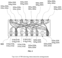
Fig. 2 shows a top view ofsubmodule 500 showing interconnection arrangements. -
Fig. 3 shows twelve of twenty-four alternative meshes that can be implemented in thesubmodule 500. All of them can provide the connectivity maps described in this application. Themesh 632 is used inFig. 7 . -
Fig. 4(a) shows a top view of DLWWOptical Chip 700. -
Fig. 4(b) shows a side view of DLWWOptical Chip 700 showing the different layers where the waveguides are written to avoid crossover. -
Fig. 5 shows a top view of DLWWOptical Chip 700. This view from the top with a 45-degree tilt showswaveguides -
Fig. 6 shows an exemplary ofmodule 900 shows connection to DLWWembodiment 700 to two fiber arrays and the connection to the multifiber ports of the module. -
Fig. 7 shows an exemplary ofmodule 400 shows connection to DLWWembodiment 700 to fiber arrays and the connection to the multifiber ports of the module. -
Fig. 8 illustrates a simple method for implementing networks with 16 Leaf Switches and up to 16 Spine switches, using themodules 400. - DLWW, a relatively new technique, can enable the fabrication of optical mesh waveguides with index contrast and circular shapes closer to single-mode fiber, SMF, so that the waveguide dimensions are comparable thereby reducing the coupling losses. Moreover, 3D geometries enabled by DLWW practically eliminate the crossover of waveguides and, therefore, the optical crosstalk among channels. However, this technology has limitations, such as propagation and bending losses, tight tolerances, and requiring a careful waveguide design.
- An advantage of the invention disclosed in this document is to provide small form factor meshes capable of supporting communication signals transmitted over multiple channels, with negligible crosstalk or noise penalties and limited excess losses beyond the designed split ratio.
- The present invention focuses on transmitters with four and eight channels, such as 400GBASE-DR4. Several embodiments will be shown in this section. Note that all the drawings are not to scale to emphasize the main features of the devices.
-
Fig. 2 shows a front view of the disclosedembodiment 500, a photonic circuit chip, which is the key element in facilitating optical network deployment, reshaping, and scaling. This embodiment is used to produce the interconnection mesh of the four groups of waveguides. As shown in this figure, there are eight parallel ports, 510, 515, 520, 525, 550, 555, 560, and 565, distributed on the front and rear sides of the embodiment. Each port consists of eight waveguides labeled from a to h. The mesh ofsubmodule 500 can be implemented in twenty-four arrangements; twelve of them are shown inFig. 3 . The interconnection arrangements for all those configurations are described in Table I. Note that for the network deployments disclosed in this document, all the twenty-four arrangements are equivalent since they preserve the correct paths from the transmitter to receivers in the network. The one shown in the embodiment example corresponds toarrangement 632. -
Fig. 4 showsembodiment 700, a variation ofarrangement 632 where all the ports are grouped in an array of fixed separation pitches, e.g., 127 µm or 250 µm. In this embodiment, the waveguides are written at different layers inside the glass, with a separation of at least 40 µm to avoid crosstalk. Some of the ports, 515, 520, 525, 550, 555, 560, and 565, are shown in the figure. For example, the eight waveguides of ports 510, 525, 550, and 565 are labeled in the figure. From the top view of the figure, it could appear that there is crossover among waveguides, e.g., waveguides 710. However, as shown inFig. 5 , viewed from the top with a 45-degree tilt, all adjacent waveguides maintain a minimum separation. InFig. 5 , there might be crossovers amongwaveguides 720; however, a view of the same waveguides with a different perspective (Fig. 4(a) ) shows no crossover among them. Waveguides described herein may have a circular cross-section shape, with refractive index contrast in the range of 0.2% to 2%.Table I Interconnection table of module 400 610 612 614 616 618 620 622 624 626 628 630 632 550a 510e 510f 510g 510g 510e 510f 510h 510h 510f 510e 510g 510h 550b 515e 515f 515g 515g 515e 515f 515h 515h 515f 515e 515g 515h 550c 520e 520f 520g 520g 520e 520f 520h 520h 520f 520e 520g 520h 550d 525e 525f 525g 525g 525e 525f 525h 525h 525f 525e 525g 525h 550e 525d 525c 525b 525b 525d 525c 525a S2Sa 525c 525d 525b 525a 550f 520d 520e 520b 520b 520d 520c 520a 520a 520c 520d 520b 520a 550g 515d 515c 515b 515b 515d 515c 515a 515a 515c 515d 515b 515a 550h 510d 510c 510b 510b 510d 510c 510a 510a 510c 510d 510b 510a 555a 510h 510e 510f 510h 510g 510e 510f 510g 510h 510f 510e 510g 555b 515h 515e 515f 515h 515g 515e 515f 515g 515h 515f 515e 515g 555c 520h 520e 520f 520b 520g 520e 520f 520g 520h 520f 520e 520g 555d 525h 525e 525f 525h 525g 525e 525f 525g 525h 525f 525e 525g 555e 525a 525d 525c 525a 525b 525d 525c 525b 525a 525c 525d 525b 555f 520a 520b 520c 520a 520b 520d 520c 520b 520a 520c 520d 520b 555g 515a 515d 515c 515a 515b 515d 515c 515b 515a 515c 515d 515b 555h 510a 510d 510c 510a 510b 510d 510c 510b 510a 510c 510d 510b 560a 510g 510h 510e 510g 510h 510g 510e 510e 510g 510h 510f 510f 560b 515g 515h 515e 515g 515h 515g 515e 515e 515g 515h 515f 515f 560c 520g 520h 520e 520g 520h 520g 520e 520e 520g 520h 520f 520f 560d 525g 525h 525e 525g 525h 525g 525e 525e 525g 525h 525f 525f 560e 525b 525a 525d 525b 525a 525b 525d 525d 525b 525a 525c 525c 560f 520b 520a 520d 520b 520a 520b 520d 520d 520b 520a 520c 520c 560g 515b 515a 515d 515b 515a 515b 515d 515d 515b 515a 515c 515c 560h 510b 510a 510d 510b 510a 510b 510d 510d 510b 510a 510c 510c 565a 510f 510g 510h 510e 510f 510h 510g 510f 510e 510g 510h 510e 565b 515f 515g 515h 515e 515f 515h 510g 515f 515e 515g 515h 515e 565c 520f 520g 520h 520e 510f 520h 520g 520f 520e 520g 520h 520e 565d 525f 525g 525h 525e 525f 525h 525g 525f 525e 525g 525h 525e 565e 525c 525b 525a 525d 525c 525a 525b 525c 525d 525b 525a 525d 565f 520c 520b 520a 520d 520c 520a 520b 520c 520d 520b 520a 520d 565g 515c 515b 515a 515d 515c 515a 515b 515d 515d 515b 515a 515d 565b 510c 510b 510a 510d 510c 510a 510b 510c 510d 510b 510a 510d - The preferred embodiments in this disclosure are written in glass utilizing the DLWW method. However, with some modification to the wavelength (or wavelengths) of light, the optics to focus the beam, the repetition rate and/or the power of the femtosecond laser, it is possible to write the disclosed waveguide designs directly on polymer (enabling flexible DLWW 3D optical circuits) and silicon substrates.
- More advanced technology may allow the waveguide to be written utilizing multiple wavelengths or variable reputation rates as the laser applies focus through the glass - this can provide waveguides with variable width or refractive index / contrast (i.e. the difference between the refractive index of the waveguide and the surrounding glass). Changing the diametrical spot size of the laser dynamically while maintaining power density allows you to change the diameter of the waveguide, while keeping the index refraction constant or variable, depending on the application. For example, up taper or a down taper that's useful for things like mode conversion, mode matching, mode filtering, stripping out modes and even multimode waveguides.
-
Fig. 6 shows an example of how to useDLWW embodiment 700 or (500) in an assembly ormodule 800, which is an enclosure that supports and protects thePLC 700, have front and rear opening for optical interfaces (connectors or adaptors), and features to organize the fiber interconnections. One or more faces of the module have multiport connectors such as MPOs, MMC, or groups of SN, MDC, or alternatively, groups of duplex connectors such as LC connectors. In the figure,module 900 has eight MPO ports evenly distributed on the front and back sides of the device. - The outputs of
DLWW device 700 are connected tofiber arrays DLWW device 700, the group of fibers from 850 is separated intogroups - The
fiber groups fiber groups element 790 can also be a mated multifiber connector pair.Fibers module 800. - Similarly, the
fiber groups fiber groups Fibers module 800. - Modules with several ports and DLWW devices, the
fiber groups fiber groups Fibers module 800. -
Module 800 incorporates a simple mesh that can support up to four Spines and four Leaf switches. Larger meshes can be implemented using methods shown in RS25595 andDLWW device 700. For example, a two-step mesh incorporated, by combining two sections where a mesh is applied to a group of fibers and then to individual fibers as shown inFig. 7 and in more detail in RS25595, increases the degree of mixing of the fiber channels inside each module. This simplifies the deployment of the network since a significant part of the network complexity is moved from the structured cabling fabric to one ormore modules 400. Table II, which shows the mesh configuration ofmodule 400, indicates that any of the sixteen parallel ports is connected to all the other parallel ports using one duplex channel. For example, in the first column of the table it is shown thatport 440 is connected to 420a, 425a,430a and 435a. By groupingseveral modules 400 and following simple rules to connect a group of uplinks or downlinks horizontally or vertically the installation becomes cleaner, and cable management is highly improved. For example,Fig. 8 shows a stack of fourmodules 400, each one with fourphotonic device 700. Part (a) of the figure shows the module side that is connected to the Leaf switches. For simplicity, we label this as the front side. Part (b) shows the opposite side of thesame module 400, the backside, which is connected to the Spine switches. It is assumed that sixteen Leaf switches, each with four MPO uplinks, need to be connected to the fabric shown in part (d) of the figure. In this illustrative example, where it is assumed that sixteen Leaf switches with four uplink each need to connect to the fabric, the connection method is described as follows. Each with the uplinks of the Leaf switches are connected horizontally in groups of four until the last port of eachmodule 400 is used. For example, 1110 and 1112, the first and the last fourth ports of thefirst module 400 connect to the uplink ports of the Leaf switches L1 and L4, respectively. The uplinks of the fifth Leaf switch populate theports 1114 of thesecond module 400. This method continues until the uplinks of the last Leaf switch are connected to theports 1116. The Spines ports are assigned at the backside of the stackedmodules 400. For example, if standalone Spine switches are used, 1120, 1122, and 1124 correspond to ports of the first, second, and sixteenth Spine switch, respectively, labeled as S1, S2, and S16.Table II Mesh configuration of module 400440 442 444 446 448 450 452 454 456 458 460 462 464 466 468 470 420a 420a 420a 420a 420b 420b 420b 420b 420c 420c 420c 420c 420d 420d 420d 420d 425a 425a 425a 425a 425b 425b 425b 425b 425c 425c 425c 425c 425d 425d 425d 425d 430a 430a 430a 430a 430b 430b 430b 430b 430c 430c 430c 430c 430d 430d 430d 430d 435a 435a 435a 435a 435b 435b 435b 435b 435c 435c 435c 435c 435d 435d 435d 435d - While this invention has been described as having a preferred design, the present invention can be further modified within the spirit and scope of this disclosure. This application is therefore intended to cover any variations, uses, or adaptations of the invention using its general principles. Further, this application is intended to cover such departures from the present disclosure as come within known or customary practice in the art to which this invention pertains and which fall within the limits of the appended claims.
Claims (13)
- An apparatus having a plurality of optical duplex and parallel fiber connector adapters,wherein one or more of the adapters are connectable to at least one of network equipment in a network, to servers, or processing units,wherein the apparatus further comprises an internal photonic circuit with an interconnection mesh,wherein the interconnection mesh matches the light path between respective transmitter adapters and receiver adapters in a network topology to provide optical connections from transmitting to receiving fibers.
- An apparatus according to claim 1, wherein the apparatus is configured to be stacked to provide Clos network topology of various radixes, the apparatus optionally having a small form factor to enable the stacking of three modules in one RU and/or to allow the stacking of up to 132 modules per rack.
- A multiport passive photonic circuit chip comprising multiple waveguides written in at a plurality of layers on a glass substrate,wherein waveguides maintain at least a minimum separation, optionally of at least 40 µm, along their trajectories,wherein one or more waveguides connect transmitting and receiving ports of an optical channel according to a mesh interconnection map.
- The photonic circuit chip of claim 3, wherein waveguides have circular cross-section shapes, with refractive index contrast in the range of 0.2% to 2%.
- An apparatus according to claim 1 or 2, wherein the internal photonic circuit with a mesh is the multiport passive photonic circuit chip of any of claims 3 to 4.
- Apparatuses having a plurality of optical duplex and parallel connector adapters, such as MPO connectors and LC adapters, where some adapters connect to network equipment in a network and others to servers or processing units such as GPUs, where the apparatuses incorporate internal photonic circuit with a mesh, wherein the light path of each transmitter and receivers is matched in order to provide proper optical connections from transmitting to receiving fibers, wherein complex arbitrary network topologies can be implemented.
- A multiport passive photonic circuit chip comprising multiple waveguides written in at several layers on a glass substrate, where waveguides maintain at least a minimum separation along all its trajectories, where some waveguides connect transmitting and receiving ports of an optical channel following a mesh interconnection map, where waveguides have circular cross-section shapes, with refractive index contrast in the range of 0.2% to 2%.
- Apparatuses according to claim 6, that can be stacked to provide Clos network topology of various radixes.
- Apparatuses according to claim 6, that can enable networks with different levels of oversubscription from 1:1 to 1:12.
- Apparatuses according to claim 6, that can be used to scale optical networks from tens to a couple of ten thousand servers.
- Apparatuses according to claim 6, that provides redundant paths for reducing the risk of network failure due to interconnection errors.
- Apparatuses according to claim 6, that have a small form factor that enables to stack of three modules in one RU, allowing the stacking of up to 132 modules per rack.
- A structured cable system comprising a stack of modules, where each module has a plurality of optical duplex and parallel connector adapters, where the apparatuses incorporate internal mesh in a chip described in claim 2, wherein the stack of modules can be used to deploy or scale various Clos network topologies using less number of interconnections.
Applications Claiming Priority (1)
| Application Number | Priority Date | Filing Date | Title |
|---|---|---|---|
| US17/989,383 US12546937B2 (en) | 2022-11-17 | 2022-11-17 | Photonic fabric chip device |
Publications (1)
| Publication Number | Publication Date |
|---|---|
| EP4372434A1 true EP4372434A1 (en) | 2024-05-22 |
Family
ID=88839184
Family Applications (1)
| Application Number | Title | Priority Date | Filing Date |
|---|---|---|---|
| EP23210503.1A Pending EP4372434A1 (en) | 2022-11-17 | 2023-11-17 | Photonic fabric chip device |
Country Status (3)
| Country | Link |
|---|---|
| US (1) | US12546937B2 (en) |
| EP (1) | EP4372434A1 (en) |
| CN (1) | CN222531785U (en) |
Citations (5)
| Publication number | Priority date | Publication date | Assignee | Title |
|---|---|---|---|---|
| US20150037032A1 (en) * | 2013-08-05 | 2015-02-05 | Telefonaktiebolaget L M Ericsson (Publ) | High Connectivity Multiple Dimension Optical Network in Glass |
| US20160025942A1 (en) * | 2013-03-12 | 2016-01-28 | Tyco Electronics Corproation | Optical waveguide module system and method |
| US20160337727A1 (en) * | 2015-05-12 | 2016-11-17 | Huawei Technologies Co., Ltd. | System and Method for Photonic Structure and Switch |
| US20180070157A1 (en) * | 2015-03-23 | 2018-03-08 | Aeponyx Inc. | Photonic switches, photonic switching fabrics and methods for data centers |
| US20210018697A1 (en) * | 2018-04-03 | 2021-01-21 | Corning Research & Development Corporation | Waveguide substrates and waveguide substrate connector assemblies having waveguides and alignment features and methods of fabricating the same |
Family Cites Families (9)
| Publication number | Priority date | Publication date | Assignee | Title |
|---|---|---|---|---|
| US9154860B2 (en) | 2014-02-11 | 2015-10-06 | Corning Optical Communications LLC | Optical interconnection assembly for spine-and-leaf network scale out |
| US11115735B2 (en) * | 2017-05-30 | 2021-09-07 | Commscope Technologies Llc | Reconfigurable optical networks |
| US11112573B2 (en) * | 2019-11-01 | 2021-09-07 | Ciena Corporation | Cooling multiple high-density network pluggable optical modules using a shared heat exchanger |
| US11635566B2 (en) * | 2019-11-27 | 2023-04-25 | Taiwan Semiconductor Manufacturing Co., Ltd. | Package and method of forming same |
| US12235526B2 (en) * | 2020-04-21 | 2025-02-25 | University Of Washington | Phase-change metasurface for programmable waveguide mode conversion |
| US11940713B2 (en) * | 2020-11-10 | 2024-03-26 | International Business Machines Corporation | Active electro-optic quantum transducers comprising resonators with switchable nonlinearities |
| GB2601172B (en) * | 2020-11-20 | 2025-02-05 | Toshiba Kk | An optical module, a system, a sending unit, a receiving unit, and a quantum communication system |
| EP4152065A1 (en) * | 2021-09-16 | 2023-03-22 | Nubis Communications, Inc. | Communication systems having co-packaged optical modules |
| US12625137B2 (en) * | 2022-01-24 | 2026-05-12 | Siphox, Inc. | Photonic biosensors for multiplexed diagnostics and a method of use |
-
2022
- 2022-11-17 US US17/989,383 patent/US12546937B2/en active Active
-
2023
- 2023-11-15 CN CN202323087868.3U patent/CN222531785U/en active Active
- 2023-11-17 EP EP23210503.1A patent/EP4372434A1/en active Pending
Patent Citations (5)
| Publication number | Priority date | Publication date | Assignee | Title |
|---|---|---|---|---|
| US20160025942A1 (en) * | 2013-03-12 | 2016-01-28 | Tyco Electronics Corproation | Optical waveguide module system and method |
| US20150037032A1 (en) * | 2013-08-05 | 2015-02-05 | Telefonaktiebolaget L M Ericsson (Publ) | High Connectivity Multiple Dimension Optical Network in Glass |
| US20180070157A1 (en) * | 2015-03-23 | 2018-03-08 | Aeponyx Inc. | Photonic switches, photonic switching fabrics and methods for data centers |
| US20160337727A1 (en) * | 2015-05-12 | 2016-11-17 | Huawei Technologies Co., Ltd. | System and Method for Photonic Structure and Switch |
| US20210018697A1 (en) * | 2018-04-03 | 2021-01-21 | Corning Research & Development Corporation | Waveguide substrates and waveguide substrate connector assemblies having waveguides and alignment features and methods of fabricating the same |
Also Published As
| Publication number | Publication date |
|---|---|
| US20240168221A1 (en) | 2024-05-23 |
| US12546937B2 (en) | 2026-02-10 |
| CN222531785U (en) | 2025-02-25 |
Similar Documents
| Publication | Publication Date | Title |
|---|---|---|
| EP1370894B1 (en) | Optical cross connect | |
| US7689079B2 (en) | Optical fiber interconnection devices and systems using same | |
| US10725245B2 (en) | High-density fabric systems interconnected with multi-port aggregated cables | |
| US7756371B1 (en) | Optical fiber interconnection devices and systems using same | |
| US6222976B1 (en) | Optical harness and cross-connect method | |
| US20150037032A1 (en) | High Connectivity Multiple Dimension Optical Network in Glass | |
| CN104040402A (en) | Lensed flexible optical interconnect for signal distribution | |
| CN112415684B (en) | Passive optical fiber cross wiring device | |
| US12546937B2 (en) | Photonic fabric chip device | |
| EP4460034A1 (en) | Extendable optical circuit switch architecture | |
| EP4382981A2 (en) | Fabric network modules | |
| US6798938B1 (en) | Routing optical matrix switching method and device | |
| US20250234117A1 (en) | Optical interconnection modules for ai networks | |
| US20210297757A1 (en) | Spatial spectral mesh | |
| US20240353628A1 (en) | Optical Interconnection Modules for High Radix Spine-Leaf Network Scale-Out | |
| US20260052327A1 (en) | Universal mesh | |
| CN222563904U (en) | Switching modules for high-radix networks | |
| US12185037B2 (en) | Optical interconnection module assembly for spine-leaf network scale-out | |
| WO2025230928A1 (en) | High density fiber assembly for optical devices | |
| Schwider et al. | Optoelectronic interconnections | |
| AU2015296847A1 (en) | Polarity configurations for parallel optics data transmission, and related apparatuses, components, systems, and methods |
Legal Events
| Date | Code | Title | Description |
|---|---|---|---|
| PUAI | Public reference made under article 153(3) epc to a published international application that has entered the european phase |
Free format text: ORIGINAL CODE: 0009012 |
|
| STAA | Information on the status of an ep patent application or granted ep patent |
Free format text: STATUS: THE APPLICATION HAS BEEN PUBLISHED |
|
| AK | Designated contracting states |
Kind code of ref document: A1 Designated state(s): AL AT BE BG CH CY CZ DE DK EE ES FI FR GB GR HR HU IE IS IT LI LT LU LV MC ME MK MT NL NO PL PT RO RS SE SI SK SM TR |
|
| STAA | Information on the status of an ep patent application or granted ep patent |
Free format text: STATUS: REQUEST FOR EXAMINATION WAS MADE |
|
| 17P | Request for examination filed |
Effective date: 20241120 |
|
| RBV | Designated contracting states (corrected) |
Designated state(s): AL AT BE BG CH CY CZ DE DK EE ES FI FR GB GR HR HU IE IS IT LI LT LU LV MC ME MK MT NL NO PL PT RO RS SE SI SK SM TR |
|
| STAA | Information on the status of an ep patent application or granted ep patent |
Free format text: STATUS: EXAMINATION IS IN PROGRESS |
|
| 17Q | First examination report despatched |
Effective date: 20260114 |