EP4369608A1 - Rf receiver - Google Patents

Rf receiver Download PDF

Info

Publication number
EP4369608A1
EP4369608A1 EP22206719.1A EP22206719A EP4369608A1 EP 4369608 A1 EP4369608 A1 EP 4369608A1 EP 22206719 A EP22206719 A EP 22206719A EP 4369608 A1 EP4369608 A1 EP 4369608A1
Authority
EP
European Patent Office
Prior art keywords
phase
oscillator
transmitter
power amplifier
output
Prior art date
Legal status (The legal status is an assumption and is not a legal conclusion. Google has not performed a legal analysis and makes no representation as to the accuracy of the status listed.)
Pending
Application number
EP22206719.1A
Other languages
German (de)
French (fr)
Inventor
Konstantinos Manetakis
Nicola Scolari
Fabio Epifano
Current Assignee (The listed assignees may be inaccurate. Google has not performed a legal analysis and makes no representation or warranty as to the accuracy of the list.)
CSEM Centre Suisse dElectronique et de Microtechnique SA Recherche et Développement
Original Assignee
CSEM Centre Suisse dElectronique et de Microtechnique SA Recherche et Développement
Priority date (The priority date is an assumption and is not a legal conclusion. Google has not performed a legal analysis and makes no representation as to the accuracy of the date listed.)
Filing date
Publication date
Application filed by CSEM Centre Suisse dElectronique et de Microtechnique SA Recherche et Développement filed Critical CSEM Centre Suisse dElectronique et de Microtechnique SA Recherche et Développement
Priority to EP22206719.1A priority Critical patent/EP4369608A1/en
Priority to US18/506,252 priority patent/US12489477B2/en
Publication of EP4369608A1 publication Critical patent/EP4369608A1/en
Pending legal-status Critical Current

Links

Images

Classifications

    • HELECTRICITY
    • H03ELECTRONIC CIRCUITRY
    • H03LAUTOMATIC CONTROL, STARTING, SYNCHRONISATION OR STABILISATION OF GENERATORS OF ELECTRONIC OSCILLATIONS OR PULSES
    • H03L7/00Automatic control of frequency or phase; Synchronisation
    • H03L7/06Automatic control of frequency or phase; Synchronisation using a reference signal applied to a frequency- or phase-locked loop
    • H03L7/08Details of the phase-locked loop
    • H03L7/099Details of the phase-locked loop concerning mainly the controlled oscillator of the loop
    • HELECTRICITY
    • H03ELECTRONIC CIRCUITRY
    • H03BGENERATION OF OSCILLATIONS, DIRECTLY OR BY FREQUENCY-CHANGING, BY CIRCUITS EMPLOYING ACTIVE ELEMENTS WHICH OPERATE IN A NON-SWITCHING MANNER; GENERATION OF NOISE BY SUCH CIRCUITS
    • H03B5/00Generation of oscillations using amplifier with regenerative feedback from output to input
    • H03B5/08Generation of oscillations using amplifier with regenerative feedback from output to input with frequency-determining element comprising lumped inductance and capacitance
    • HELECTRICITY
    • H03ELECTRONIC CIRCUITRY
    • H03FAMPLIFIERS
    • H03F3/00Amplifiers with only discharge tubes or only semiconductor devices as amplifying elements
    • H03F3/189High-frequency amplifiers, e.g. radio frequency amplifiers
    • H03F3/19High-frequency amplifiers, e.g. radio frequency amplifiers with semiconductor devices only
    • H03F3/195High-frequency amplifiers, e.g. radio frequency amplifiers with semiconductor devices only in integrated circuits
    • HELECTRICITY
    • H03ELECTRONIC CIRCUITRY
    • H03FAMPLIFIERS
    • H03F3/00Amplifiers with only discharge tubes or only semiconductor devices as amplifying elements
    • H03F3/20Power amplifiers, e.g. Class B amplifiers, Class C amplifiers
    • H03F3/24Power amplifiers, e.g. Class B amplifiers, Class C amplifiers of transmitter output stages
    • H03F3/245Power amplifiers, e.g. Class B amplifiers, Class C amplifiers of transmitter output stages with semiconductor devices only
    • HELECTRICITY
    • H03ELECTRONIC CIRCUITRY
    • H03FAMPLIFIERS
    • H03F3/00Amplifiers with only discharge tubes or only semiconductor devices as amplifying elements
    • H03F3/45Differential amplifiers
    • H03F3/45071Differential amplifiers with semiconductor devices only
    • H03F3/45076Differential amplifiers with semiconductor devices only characterised by the way of implementation of the active amplifying circuit in the differential amplifier
    • H03F3/45179Differential amplifiers with semiconductor devices only characterised by the way of implementation of the active amplifying circuit in the differential amplifier using MOSFET transistors as the active amplifying circuit
    • H03F3/45183Long tailed pairs
    • HELECTRICITY
    • H04ELECTRIC COMMUNICATION TECHNIQUE
    • H04BTRANSMISSION
    • H04B1/00Details of transmission systems, not covered by a single one of groups H04B3/00 - H04B13/00; Details of transmission systems not characterised by the medium used for transmission
    • H04B1/02Transmitters
    • H04B1/04Circuits
    • H04B1/0475Circuits with means for limiting noise, interference or distortion
    • HELECTRICITY
    • H04ELECTRIC COMMUNICATION TECHNIQUE
    • H04BTRANSMISSION
    • H04B17/00Monitoring; Testing
    • H04B17/10Monitoring; Testing of transmitters
    • H04B17/11Monitoring; Testing of transmitters for calibration
    • H04B17/13Monitoring; Testing of transmitters for calibration of power amplifiers, e.g. gain or non-linearity
    • HELECTRICITY
    • H03ELECTRONIC CIRCUITRY
    • H03FAMPLIFIERS
    • H03F2200/00Indexing scheme relating to amplifiers
    • H03F2200/451Indexing scheme relating to amplifiers the amplifier being a radio frequency amplifier
    • HELECTRICITY
    • H03ELECTRONIC CIRCUITRY
    • H03FAMPLIFIERS
    • H03F2203/00Indexing scheme relating to amplifiers with only discharge tubes or only semiconductor devices as amplifying elements covered by H03F3/00
    • H03F2203/45Indexing scheme relating to differential amplifiers
    • H03F2203/45501Indexing scheme relating to differential amplifiers the CSC comprising a L-C parallel resonance circuit
    • HELECTRICITY
    • H03ELECTRONIC CIRCUITRY
    • H03FAMPLIFIERS
    • H03F2203/00Indexing scheme relating to amplifiers with only discharge tubes or only semiconductor devices as amplifying elements covered by H03F3/00
    • H03F2203/45Indexing scheme relating to differential amplifiers
    • H03F2203/45731Indexing scheme relating to differential amplifiers the LC comprising a transformer
    • HELECTRICITY
    • H04ELECTRIC COMMUNICATION TECHNIQUE
    • H04BTRANSMISSION
    • H04B1/00Details of transmission systems, not covered by a single one of groups H04B3/00 - H04B13/00; Details of transmission systems not characterised by the medium used for transmission
    • H04B1/02Transmitters
    • H04B1/04Circuits
    • H04B2001/0408Circuits with power amplifiers

Definitions

  • the present invention concerns a radio-frequency (RF) transmitter.
  • RF radio-frequency
  • RF radio-frequency
  • RF transmitters are well known and widely used, in communication devices (e.g., in portable or wearable devices), to perform signal transmission over one or multiple frequency bands according to communication standards, as for example Bluetooth (BT), Bluetooth Low Energy (BLE), WCDMA, CDMA, GSM, LTE standards for cellular telephony, IEEE 802.11 protocols for wireless LAN, etc.
  • Bluetooth Bluetooth
  • BLE Bluetooth Low Energy
  • WCDMA Wideband Code Division Multiple Access
  • CDMA Code Division Multiple Access
  • GSM Global System for Mobile communications
  • LTE Long Term Evolution
  • IEEE 802.11 protocols for wireless LAN etc.
  • FIG. 1 shows a known transmitter 1'. It comprises a phase locked loop (PLL) 20', which could be an all-digital PLL (ADPLL) and comprises a phase detector (PD) 201', followed by a loop filter (FL) 202' and an oscillator (a voltage controlled oscillator or VCO in the example) 203'.
  • PLL phase locked loop
  • PD phase detector
  • FL loop filter
  • oscillator a voltage controlled oscillator or VCO in the example
  • the oscillator 203' generates a frequency which is the double of the transmitted frequency at the antenna 50'. This frequency is then divided by 2 by a divider 30' and fed to a power amplifier (PA) 40', whose output is connected to the antenna 50'.
  • PA power amplifier
  • the second harmonic of the PA's current is at the same frequency as the oscillator, resulting in pushing and/or pulling.
  • pushing is due to coupling from the PA to the oscillator electrical ports (supply, ground, etc.) and/or to the substrate; pulling is due to the magnetic coupling from the PA to the oscillator tank.
  • the oscillator frequency is shifted away from the wanted value.
  • the PLL tries then to correct for the frequency shift, but it is in general not fast enough.
  • EVM Error Vector Magnitude
  • Pulling can be estimated from EM simulations, but an accurate absolute prediction is very difficult.
  • the pulling due to magnetic coupling from the PA to the oscillator can be estimated with the model shown in the Figure 2 .
  • An oscillator in general comprises:
  • the tank circuit provides a resonant frequency.
  • the tank circuit comprises an inductor and a capacitor, and the oscillator is named "LC-tuned oscillator.” It can comprise a common mode part and a differential part and then a differential respectively common-mode tank impedance.
  • An LC-tuned oscillator 203' is modelled in the Figure 2 with a tank parallel circuit comprising the inductor L 1 and the capacitor C.
  • the tank parallel loss is modelled with the tank parallel loss resistance R p and the active circuit with the transconductances g 1 and g 3 .
  • An aim of the present invention is the provision of a RF transmitter that overcomes the shortcomings and limitations of the state of the art.
  • Another aim of the invention is the provision of a RF transmitter wherein pushing and/or pulling is(are) alleviated.
  • Another aim of the invention is the provision of a RF transmitter wherein pushing and/or pulling is(are) efficiently alleviated.
  • the RF transmitter according to the invention comprises:
  • the RF transmitter comprises a phase shifter module between the phase-locked loop and the power amplifier, arranged to introduce a phase shift between the oscillator carrier and a harmonic of the power amplifier current, in order to reduce a frequency shift of the oscillator carrier due to pushing and/or pulling.
  • the proposed RF transmitter offers significant performance benefits in terms of modulation quality metrics such as EVM and/or spectral regrowth.
  • the RF transmitter comprises a divider connected to the output of the oscillator and being arranged to divide the frequency of the oscillator carrier by a number, e.g. an integer and positive number, the phase shifter module being between the divider and the power amplifier. In one embodiment, this number is equal to two.
  • the RF transmitter comprises a divider connected to the output of the oscillator and being arranged to divide the frequency of the oscillator carrier by a number, e.g. an integer and positive number, the phase shifter module being between phase-locked loop and the divider. In one embodiment, this number is equal to two.
  • the phase shifter module is arranged to introduce a phase shift between the oscillator carrier and the second harmonic of the power amplifier current.
  • the phase shifter module is arranged to introduce a phase shift between the oscillator carrier and the Nth harmonic of the power amplifier current.
  • the phase shifter module is arranged to introduce a phase shift between the oscillator carrier and the first harmonic of the power amplifier current.
  • the phase shift of the phase shifter module is a variable phase shift, i.e. the phase shift can be varied, e.g. automatically varied.
  • the RF transmitter comprises a computing unit and an oscillator frequency shift measurement unit, wherein:
  • variable phase shift takes different values by stepping the phase shift, as the frequency shift is not monotonic with the phase shift.
  • the measurement unit is the phase-locked loop.
  • the phase-locked loop is an all-digital phase-locked loop.
  • the phase-locked loop comprises a phase detector module and an additional module connected to an output of the phase detector module, the additional module being arranged so as to compute the oscillator frequency shift.
  • the phase shifter module comprises several selectable delay cells, each delay cell comprising several inverters.
  • each delay cell comprises back-to-back inverters so as to control the duty-cycle of a clock arranged to drive the PA. Controlling this duty cycle allows to control (and in particular minimize) the level of the second harmonic current of the power amplifier, which is inherent in this clock.
  • the inverters comprise transistors, the phase shifter module comprising a control module, arranged to control a fourth terminal of at least some transistors for temperature compensation.
  • the fourth terminal is the terminal allowing to modify a threshold voltage of the transistor.
  • the fourth terminal is the bulk terminal of those transistor.
  • the fourth terminal is the back gate terminal of the transistors.
  • the fourth terminal is one of the two gate terminals
  • control module comprises:
  • the fourth terminal of the N-type transistor has a PTAT (proportional to absolute temperature) behaviour
  • the fourth terminal of the P-type transistor has a CTAT (complementary to absolute temperature) behaviour.
  • the computing unit is arranged to build a frequency shift - signal envelope look-up table.
  • the signal envelope is the envelope of the PA output (AM) modulation signal.
  • a predistortion signal based on said look-up table is added to an oscillator frequency control input, in order to reduce further the frequency shift of the oscillator carrier due to pushing and/or pulling.
  • an inductor of the oscillator is designed so as to reduce a magnetic coupling between the inductor and a balun of the power amplifier, an oscillator electrical port and/or a substrate.
  • the inductor has an eight shape.
  • the distance and orientation between the oscillator inductor and the balun of the power amplifier is(are) arranged so as to reduce said magnetic coupling.
  • the power amplifier comprises a power amplifier decoupling capacitor and a tank (or filter), the tank sharing a terminal with a terminal of the decoupling capacitor and having an impendence at the harmonic equal or higher than 100 ⁇ , in particular equal or higher than a few hundred ohms, for example equal or higher than 1 K ⁇ in order to reduce or impede a flow of said harmonic current to reach the power amplifier decoupling capacitor.
  • harmonic refers to a harmonic of the power amplifier current, unless otherwise specified.
  • FIG. 3 shows one embodiment of a RF transmitter 1 according to the invention.
  • the RF transmitter 1 according to the invention comprises:
  • the RF transmitter comprises a phase shifter module 10 between the phase-locked loop 20 and the power amplifier 40, arranged to introduce a phase shift between the oscillator carrier and a harmonic of the power amplifier current, in order reduce a frequency shift of the oscillator carrier due to pushing and/or pulling.
  • the proposed RF transmitter offers significant performance benefits in terms of modulation quality metrics such as EVM and/or spectral regrowth.
  • phase shifter module 10 allows the PA current to be in phase or in anti-phase with the oscillator carrier, which results in no frequency pulling or in a reduced frequency pulling.
  • phase shifter module 10 Effectively adjusting the phase shift ⁇ of the phase shifter module 10 allows to operate under the condition sin( ⁇ 2+ ⁇ ) ⁇ 0 in formula (9), thus minimizing pulling.
  • the RF transmitter 1 comprises a divider 30 connected to the output of the oscillator of the PLL 20 and being arranged to divide the frequency of the oscillator carrier by a number, e.g. an integer and positive number (two in the embodiment of Figure 3 ), and the phase shifter module 10 is between the divider 30 and the power amplifier 40.
  • the phase shifter module 10 is between phase-locked loop 20 and the divider 30.
  • the phase shifter module 10 is arranged to introduce a phase shift between the oscillator carrier and the Nth harmonic of the power amplifier current.
  • phase shifter module 10 is arranged to introduce a phase shift between the oscillator carrier and the first harmonic of the power amplifier current.
  • the phase shift of the phase shifter module is a variable phase shift, i.e. the phase shift can be varied.
  • the second harmonic of the PA usually exhibits wide AM-AM and AM-PM, wherein as usual AM indicates an amplitude modulation (modulation format with variable envelope) and PM a phase modulation.
  • AM indicates an amplitude modulation (modulation format with variable envelope)
  • PM a phase modulation.
  • Both the PA second harmonic current amplitude and the PA second harmonic current phase depend on the modulation envelope r(t).
  • Figure 4 shows the PA first and second harmonic current magnitudes in mA against load power in dBm for one embodiment of the RF transmitter according to the invention.
  • Figure 5 which shows the PA second harmonic phase in degrees against load power in dBm for one embodiment of the RF transmitter according to the invention.
  • Figure 6 shows the LC-tuned oscillator frequency shift after the divider 30 due to the combined effect of pushing from the first PA harmonic H 1 in KHz and pulling from the second PA harmonic H 2 in KHz against load power in dBm for one embodiment of the RF transmitter according to the invention.
  • Formula (11) contains with respect to formula (10) an additional pushing term k ⁇ i 1 (r), for taking into account the pushing effect for low output power levels.
  • phase shifter module 10 allows to reduce a frequency shift of the oscillator carrier due to pushing effect as well.
  • the peak to peak frequency shift in Figure 6 is indicated as ⁇ f pp .
  • Figure 7 shows the LC-tuned oscillator frequency in KHz after the divider with different values of the phase shifter module ( ⁇ ) against load power in dBm for one embodiment of the RF transmitter according to the invention.
  • the step to find an optimum value for the phase shifter module is done during the RF transmitter start-up.
  • the PA 40 is ramped up repeatedly and the algorithm steps ⁇ and seeks to find the minimum peak-peak frequency shift ⁇ f pp .
  • the RF transmitter comprises a computing unit (not illustrated) and an oscillator frequency shift measurement unit (not illustrated), wherein
  • variable phase shift ⁇ takes different values by stepping the phase shift, as the frequency shift is not monotonic with the phase shift ⁇ .
  • the calibration can effectively compensate for process and supply variation in the RF transmitter 1. After the calibration, only temperature may affect the phase shifter module.
  • Figure 8A shows one embodiment of the phase shifter module 10 of the RF transmitter 1 according to the invention. It comprises two lines (for a differential control), each lines comprising one or more cells 100 (five in Figure 8A ), the phase shifter module 10 being arranged so as to select a specific cell 100 via the terminals sel ⁇ 0>, sel ⁇ 1>, sel ⁇ 2>, etc. and then have a specific phase shift according to the needs.
  • the back-to-back inverters 102 between the two lines are not necessary for introducing the phase shift. However, where present, they allow to control the duty-cycle of a clock arranged to drive the PA 50. Controlling this duty cycle allows to control (and in particular minimize) the level of the H 2 component of the power amplifier, which is inherent in this clock, as illustrated in Figure 9 , which shows the duty-cycle of the clock that drives the PA in percentage against the difference between the PA first H 1 and second harmonic H 2 in dBc. In one embodiment, back-to-back inverters 102 guarantee 50% duty cycle.
  • FIG 8B shows one embodiment of the internals of the individual delay cells 100 of the phase shifter module 10 of Figure 8A .
  • Each cell 100 comprises N inverters 1000, wherein N could be equal for example to 2, 4, 6, 16, 32.
  • a multiplexer MUX and the selection signal sel allow to select if a delay N is introduced, or if there is no delay.
  • Figure 8C shows one embodiment of the individual (and known) inverter 1000 of an individual delay cell 100 of Figure 8B .
  • phase shifter module only temperature may affect the phase shifter module.
  • (individual or collective) control of the fourth terminals bgp and bgn inverters' P- respectively N-transistors allows for temperature compensation of the overall phase shift.
  • the phase shifter module 10 comprises a control module 104, illustrated in Figure 10A , arranged to control the fourth terminals bgp and bgn of at least some transistors of the inverters 1000 for temperature compensation.
  • the fourth terminal is the terminal allowing to modify a threshold voltage of the transistor.
  • the fourth terminal is the bulk terminal of those transistor.
  • the fourth terminal is the back gate terminal of the transistors.
  • the fourth terminal is one of the two gate terminals
  • control module 104 comprises:
  • the potentiometer 1042 is placed between a current source 1043 and the ground.
  • the temperature sensor 1041 is arranged to control the p-output bgp and the n-output bgn, and the n-output and the p-output are arranged to (collectively) control the fourth terminals of the N-type respectively P-type transistors of the inverters 1000.
  • the temperature sensor 1041 controls two separate outputs bgp and bgn of a (digital) potentiometer. These outputs (collectively) control the -output bgp and a n-output bgn in inverters 1000 of the phase shifter module 10.
  • the temperature steps provided by the temperature sensor 1041 are in the range of 10 °C to 20 °C.
  • Figure 10B shows that, in one embodiment, the p-output bgp of the control module 104 of Figure 10A exhibits a CTAT behaviour, while the n-output bgn exhibits a PTAT behaviour.
  • FIG 11 shows one embodiment of a RF transmitter 1 according to the invention.
  • the PLL 20 is an ADPLL and the phase shifter module 10 is placed between the divider by two 30 and the power amplifier 40, with its phase modulation and amplitude modulation paths.
  • the output of the phase shifter module 10 is connected (directly connected in Figure 11 ) to the phase modulation path of the power amplifier 40.
  • the phase shifter module 10 comprises one input sel ⁇ 4:0> for selecting the desired phase shift and two inputs bgp and bgn for the temperature control.
  • the measurement unit is the phase-locked loop. In one embodiment, the measurement unit is an all digital phase-locked loop.
  • Figure 12 shows one embodiment of a s-domain, type-II model all digital phase-locked loop for measuring the frequency shift of the LC-tuned oscillator as the PA power ramps up.
  • the s-domain, type-II model all digital phase-locked loop of Figure 12 should not be considered as limitative, and other types of PLL could be used instead.
  • the use of an all digital phase-locked loop is not essential for the embodiment of Figure 12 .
  • the phase-locked loop comprises an additional module (reference 205 in Figure 12 ) connected to an output of the phase detector module 201, the additional module 205 being arranged to compute the oscillator frequency shift.
  • the additional module 205 cancels out the (AD)PLL dynamics. These dynamics are known once the (AD)PLL calibration is already finished.
  • the bandwidth of the measurement is f p . It can be set depending on the PA ramp up speed and is not limited by the ADPLL bandwidth.
  • Figure 13 shows the frequency shift in KHz and the measured value in KHz against time in ⁇ s at the output of the additional module 205 of Figure 12 .
  • K DCO is set to 25 KHz/step.
  • the output out of the additional module 205 is directly proportional to the frequency shift ⁇ f shift and indirectly proportional to the oscillator gain K DCO .
  • Figure 14 shows a constellation for an BT EDR version 2 modulation given the frequency shift of Figure 13 . It is possible to note the spreading of the constellation with regard to the ideal bits (each one being represented by a cross).
  • Figure 15 shows a spectrum for an BT EDR version 2 modulation given the frequency shift of Figure 13 .
  • the estimated EVM is 9.3% (the ADPLL bandwidth is 200 KHz).
  • the computing unit is arranged to build a frequency shift - signal envelope look-up table.
  • the signal envelope is the envelope of the PA output (AM) modulation signal.
  • a predistortion signal based on said look-up table is added to an oscillator frequency control input, in order to reduce further the frequency shift of the oscillator carrier due to pushing and/or pulling.
  • phase shifter module has already set the phase shift to its optimal value to guarantee minimal remaining frequency shift.
  • the PLL can be used to sample the remaining frequency shift. It is possible thus to build a [frequency shift - signal envelope] look-up table during the ramp up.
  • This information is subsequently used during the remaining part of the frame as a AM-FM predistortion signal added to the VCO frequency control input, in order to cancel the frequency shift due to pushing/pulling.
  • the measured frequency shift and the lookup table values (4-bits) are shown in the Figure 16 . Some values of a [frequency shift - signal envelope] look-up table are shown as well. In this embodiment, a 4-bit look-up table is used.
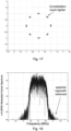
  • Figure 17 shows a constellation for an BT EDR version 2 modulation after an AM-FM digital predistortion
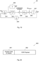
  • Figure 18 shows a spectrum for an BT EDR version 2 modulation after the AM-FM digital predistortion as in Figure 17 .
  • the estimated EVM is 1.8%, exhibiting a significant reduction (the ADPLL bandwidth is 200KHz). It is possible to see in Figure 17 and 18 improvements can be observed in the constellation (which is much tighter) and the spectral regrowth, with regard to the constellation and the spectral regrowth of Figures 14 respectively 15 (without AM-FM predistortion).
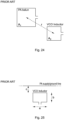
  • FIG 19 shows one embodiment of an ADPLL 20 with a predistortion correction of the RF transmitter according to the invention.
  • a predistortion correction 208 is added between the loop filter 202 and the oscillator 203.
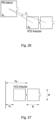
  • FIG 20 shows a simplified BT EDR packet structure 800.
  • Access Code & Header portion 801 uses e.g. a GFSK modulation.
  • the PA envelop ramps up.
  • the PLL is used to sample the remaining frequency shift, in order to build a [frequency shift - signal envelope] look-up table.
  • This information is subsequently used during the EDR portion 802 of the packet 800 as a predistortion signal added (as for example illustrated in Figure 19 ) to the oscillator frequency control input, in order to cancel the frequency shift due to pushing/pulling.
  • Figure 21 shows one embodiment of a charge pump PLL 20 of the RF transmitter according to the invention.
  • the charge pump PLL 20 of Figure 21 comprises an ADC 209 which converts to digital the voltage at the oscillator (VCO) input.
  • the charge pump PLL 20 of Figure 21 is an alternative embodiment to the PLL of Figure 12 .
  • Figure 22 shows the charge pump PLL of Figure 21 , with a possible implementation of a predistortion correction.
  • the predistortion correction is added to the oscillator input using a DAC 210.
  • the charge pump PLL 20 of Figure 22 is an alternative embodiment to the PLL of Figure 19 .
  • Figure 23 shows one embodiment of a PA 40 of the RF transmitter according to the invention, comprising a tank 400 arranged to impede a flow of a harmonic current (e.g. of the second harmonic PA current H 2 ) before it reaches a power amplifier decoupling capacitor C dec .
  • a harmonic current e.g. of the second harmonic PA current H 2
  • the additional tank 400 illustrated comprises an inductor and a capacitor in parallel. It presents an impendence at the harmonic equal or higher than 100 ⁇ , in particular equal or higher than a few hundred ohms, for example equal or higher than 1 K ⁇ , at the harmonic current and impedes then the flow of the second harmonic PA current before it reaches the decoupling capacitor C dec .
  • the tank 400 could be placed between the active part comprising transistors M1 and M2 and a fixed voltage (e.g. the ground in Figure 23 ). In complement or in alternative, the tank can be placed in correspondence of the PA balun, as indicated by the arrow in Figure 23 . In both cases, the tank 400 shares a terminal with a terminal of the coupling capacitor Cdec.
  • Figure 24 shows a known magnetic coupling from a PA balun to a LC-tuned oscillator's inductor.
  • Figure 25 shows a known magnetic coupling from PA ground/supply lines to a LC-tuned oscillator's inductor.
  • the magnetic coupling from the PA to the LC-tuned oscillator can be either:
  • Figures 26 to 30 show a possibility to further minimize pushing/pulling both at the PA and the oscillator by circuit design techniques and/or careful layout.
  • Figure 26 shows a magnetic coupling from the PA balun to the LC-tuned oscillator's inductor according to one embodiment of the invention.
  • the aim of this embodiment is to design the oscillator's inductor in a magnetically immune fashion.
  • the inductor of the oscillator is designed so as have an eight shape.
  • a good immunity can be achieved for sufficiently large separations for which r 1 ⁇ r 2 according to the following formula: M ⁇ ⁇ A 1 A 2 4 ⁇ 1 r 1 3 ⁇ 1 r 2 3 wherein r 1 , r 2 are the distances between the centers of each half-eight of the oscillator's inductor and the center of the PA balun.
  • Figure 27 shows a magnetic coupling from PA ground/supply lines to a LC-tuned oscillator's inductor according to one embodiment of the invention.
  • a good immunity can be achieved for sufficiently large separations for which c 1 ⁇ c 2 according to the following formula: M ⁇ ⁇ a b 2 ⁇ 1 c 1 ⁇ 1 c 2 wherein c 1 , c 2 are the distances between each half-eight of the oscillator's inductor and PA ground/supply lines.
  • Figure 28 shows a magnetic coupling from the PA balun to the LC-tuned oscillator's inductor according to one embodiment of the invention (symmetrical placing).
  • Figure 29 shows magnetic coupling from PA ground/supply lines to a LC-tuned oscillator's inductor according to one embodiment of the invention (symmetrical placing).
  • Figure 30 shows magnetic coupling from PA ground/supply lines laid out in pairs to a LC-tuned oscillator's inductor according to one embodiment of the invention.
  • supply/ground lines emanating from the PA can be made magnetically immune if they are laid out in pairs, according to the following formula: M ⁇ ⁇ a 2 ⁇ b ⁇ c b + c c wherein ⁇ c is the distance between each supply/ground line of the pair.
  • Pushing of the oscillator could also be minimized with careful grounding, good local decoupling, and star-routing of supplies/grounds. Additionally, regulators help to provide adequate power supply rejection (PSR) and/or boost the immunity of the oscillator to external disturbances.
  • PSR power supply rejection

Landscapes

  • Engineering & Computer Science (AREA)
  • Computer Networks & Wireless Communication (AREA)
  • Signal Processing (AREA)
  • Physics & Mathematics (AREA)
  • Power Engineering (AREA)
  • Nonlinear Science (AREA)
  • Electromagnetism (AREA)
  • Microelectronics & Electronic Packaging (AREA)
  • Transmitters (AREA)

Abstract

The present invention concerns a RF transmitter (1) comprising:- a phase-locked loop (20), comprising an oscillator arranged to output an oscillator carrier,- a power amplifier (40), arranged to conduct a power amplifier current, characterised in that the RF transmitter comprises:- a phase shifter module (10) between the phase-locked loop (20) and the power amplifier (40), arranged to introduce a phase shift between the oscillator carrier and a harmonic of the power amplifier current, in order reduce a frequency shift of the oscillator carrier due to pushing and/or pulling.

Description

    Technical domain
  • The present invention concerns a radio-frequency (RF) transmitter.
  • Related art
  • In this context the term "RF" or the expression "radio-frequency" indicates a range of frequencies between 3 kHz and 300 GHz, in particular between 300 MHz and 100 GHz.
  • RF transmitters are well known and widely used, in communication devices (e.g., in portable or wearable devices), to perform signal transmission over one or multiple frequency bands according to communication standards, as for example Bluetooth (BT), Bluetooth Low Energy (BLE), WCDMA, CDMA, GSM, LTE standards for cellular telephony, IEEE 802.11 protocols for wireless LAN, etc.
  • Figure 1 shows a known transmitter 1'. It comprises a phase locked loop (PLL) 20', which could be an all-digital PLL (ADPLL) and comprises a phase detector (PD) 201', followed by a loop filter (FL) 202' and an oscillator (a voltage controlled oscillator or VCO in the example) 203'. The signal generated by the oscillator 203' is divided by a number N at a divider 204' and fed back to the phase detector 201', which compares it to a reference signal REF.
  • In the example of Figure 1, the oscillator 203' generates a frequency which is the double of the transmitted frequency at the antenna 50'. This frequency is then divided by 2 by a divider 30' and fed to a power amplifier (PA) 40', whose output is connected to the antenna 50'.
  • In this case, the second harmonic of the PA's current is at the same frequency as the oscillator, resulting in pushing and/or pulling.
  • In general, pushing is due to coupling from the PA to the oscillator electrical ports (supply, ground, etc.) and/or to the substrate; pulling is due to the magnetic coupling from the PA to the oscillator tank.
  • As the PA power is increased, the oscillator frequency is shifted away from the wanted value. The PLL tries then to correct for the frequency shift, but it is in general not fast enough.
  • This results in performance deterioration in terms of modulation quality metrics such as Error Vector Magnitude (EVM) and/or spectral regrowth.
  • Pulling can be estimated from EM simulations, but an accurate absolute prediction is very difficult. The pulling due to magnetic coupling from the PA to the oscillator can be estimated with the model shown in the Figure 2.
  • An oscillator in general comprises:
    • a tank circuit, and
    • an active circuit (or active device) connected to the tank circuit, the active circuit comprising transistors.
  • The tank circuit provides a resonant frequency. In general, the tank circuit comprises an inductor and a capacitor, and the oscillator is named "LC-tuned oscillator." It can comprise a common mode part and a differential part and then a differential respectively common-mode tank impedance.
  • The active circuit allows to sustain the oscillation of the tank circuit. It can be modelled as a nonlinear transconductor G(V): G V = g 1 V + g 2 V 2 + g 3 V 3
    Figure imgb0001
    wherein
    • V is the differential voltage across the active circuit, which in general correspond to the voltage across the tank circuit
    • g1 is the first-order transconductance of the active circuit as a whole g2 is the second-order transconductance of the active circuit as a whole g3 is the third-order transconductance of the active circuit as a whole.
  • An LC-tuned oscillator 203' is modelled in the Figure 2 with a tank parallel circuit comprising the inductor L1 and the capacitor C. The tank parallel loss is modelled with the tank parallel loss resistance Rp and the active circuit with the transconductances g1 and g3. The inductor L1 is coupled with the inductor L2 of the balun of the PA 40' according to the following formula: k = M L 1 L 2
    Figure imgb0002
    where M is the mutual inductance between L1 and L2.
  • Starting from the phase-dynamics equation describing the evolution of the LC-tuned oscillator phase, and considering an injection current iinj into the tank of the LC-tuned oscillator due to the PA, as shown in the lower part of Figure 2, it is possible to obtain the following equations: v = V p sin ωt
    Figure imgb0003
    dt = ω o + i inj cos ω t V p C
    Figure imgb0004
    i inj = i M L 1 sin ω t + Δϕ
    Figure imgb0005
    ω o 1 LC
    Figure imgb0006
    wherein
    • v is the oscillator voltage
    • Vp is the oscillator peak voltage
    • ω is the oscillator carrier frequency
    • t is the time
    • θ is the oscillator phase
    • ω0 is the undisturbed oscillator carrier frequency
    • Δϕ is injection current phase shift
    • i inj is the injection current into the tank due to the PA
    • i is the current into the tank.
  • This gives what is known in the literature as the Adler's formula: ω = ω o + i . M L 1 2 C V p sin Δϕ
    Figure imgb0007
    which can be rewritten as: ω = ω o + Δω p sin Δϕ
    Figure imgb0008
    wherein Δωp is the oscillator peak pulling.
  • For example, with PA second harmonic current i = 10 mA, VCO component values L1 = 1.45 nH and C = 700 fF (for 5 GHz center frequency), VCO peak swing Vp = 1 V, the tiny amount of mutual inductance M = 2.6 pH results in about 2MHz peak pulling. Minute amounts of magnetic coupling result then in sizeable frequency shifts Δωp .
  • Therefore, there is a need of alleviate pushing and/or pulling in RF transmitters.
  • There is a need of efficiently alleviate pushing and/or pulling in RF transmitters.
  • Short disclosure of the invention
  • An aim of the present invention is the provision of a RF transmitter that overcomes the shortcomings and limitations of the state of the art.
  • Another aim of the invention is the provision of a RF transmitter wherein pushing and/or pulling is(are) alleviated.
  • Another aim of the invention is the provision of a RF transmitter wherein pushing and/or pulling is(are) efficiently alleviated.
  • According to the invention, these aims are attained by the object of the attached claims, and especially by the RF transmitter of claim 1, whereas dependent claims deal with alternative and preferred embodiments of the invention.
  • The RF transmitter according to the invention comprises:
    • a phase-locked loop, comprising an oscillator arranged to output an oscillator carrier, and
    • a power amplifier, arranged to conduct a power amplifier current.
  • According to the invention, the RF transmitter comprises a phase shifter module between the phase-locked loop and the power amplifier, arranged to introduce a phase shift between the oscillator carrier and a harmonic of the power amplifier current, in order to reduce a frequency shift of the oscillator carrier due to pushing and/or pulling.
  • Thanks to the presence of the claimed phase shifter module, frequency shifts of the oscillator carrier due to pushing and/or pulling are efficiently reduced: the proposed RF transmitter offers significant performance benefits in terms of modulation quality metrics such as EVM and/or spectral regrowth.
  • In one embodiment, the RF transmitter comprises a divider connected to the output of the oscillator and being arranged to divide the frequency of the oscillator carrier by a number, e.g. an integer and positive number, the phase shifter module being between the divider and the power amplifier. In one embodiment, this number is equal to two.
  • In one embodiment, the RF transmitter comprises a divider connected to the output of the oscillator and being arranged to divide the frequency of the oscillator carrier by a number, e.g. an integer and positive number, the phase shifter module being between phase-locked loop and the divider. In one embodiment, this number is equal to two.
  • In both the embodiments comprising the divider, if the divider is arranged to divide the frequency of its input signal by two, the phase shifter module is arranged to introduce a phase shift between the oscillator carrier and the second harmonic of the power amplifier current.
  • In general, in both the embodiments comprising the divider, if the divider is arranged to divide the frequency of its input signal by an integer number N, the phase shifter module is arranged to introduce a phase shift between the oscillator carrier and the Nth harmonic of the power amplifier current.
  • In the absence of a divider, the phase shifter module is arranged to introduce a phase shift between the oscillator carrier and the first harmonic of the power amplifier current.
  • In one embodiment, the phase shift of the phase shifter module is a variable phase shift, i.e. the phase shift can be varied, e.g. automatically varied.
  • In one embodiment, the RF transmitter comprises a computing unit and an oscillator frequency shift measurement unit, wherein:
    • the power amplifier is arranged to be ramped-up during a calibration phase,
    • the phase shifter module is arranged so that during this calibration phase, the variable phase shift takes different values,
    • the measurement unit is arranged to measure the oscillator frequency shift against a load power for each value of the phase shift,
    • the computing unit is arranged to select the value of the phase shift minimizing a peak-peak oscillator frequency shift against the load power.
  • In one embodiment, the variable phase shift takes different values by stepping the phase shift, as the frequency shift is not monotonic with the phase shift.
  • In one embodiment, the measurement unit is the phase-locked loop.
  • In one embodiment, the phase-locked loop is an all-digital phase-locked loop.
  • In one embodiment, the phase-locked loop comprises a phase detector module and an additional module connected to an output of the phase detector module,
    the additional module being arranged so as to compute the oscillator frequency shift.
  • In one embodiment, the phase shifter module comprises several selectable delay cells, each delay cell comprising several inverters.
  • In one embodiment, each delay cell comprises back-to-back inverters so as to control the duty-cycle of a clock arranged to drive the PA. Controlling this duty cycle allows to control (and in particular minimize) the level of the second harmonic current of the power amplifier, which is inherent in this clock.
  • In one embodiment, the inverters comprise transistors, the phase shifter module comprising a control module, arranged to control a fourth terminal of at least some transistors for temperature compensation.
  • In this context, the fourth terminal is the terminal allowing to modify a threshold voltage of the transistor. In one embodiment, the fourth terminal is the bulk terminal of those transistor. In another embodiment, in particular if the transistors are realised in the technology silicon on insulator (SOI) or fully depleted silicon on insulator (FDSOI), the fourth terminal is the back gate terminal of the transistors. In another embodiment in which the transistors comprise two gate terminals, the fourth terminal is one of the two gate terminals
  • In one embodiment, the control module comprises:
    • a temperature sensor,
    • a potentiometer comprising a p-output and a n-output,
    • the temperature sensor being arranged to control the n-output and the p-output,
    • the n-output and the p-output being arranged to collectively control the fourth terminals of the N-type respectively P-type transistors of the inverters.
  • In one embodiment, the fourth terminal of the N-type transistor has a PTAT (proportional to absolute temperature) behaviour, and the fourth terminal of the P-type transistor has a CTAT (complementary to absolute temperature) behaviour.
  • In one embodiment, as the power amplifier is ramped up and the measurement unit measures the frequency shift, the computing unit is arranged to build a frequency shift - signal envelope look-up table. In this context, the signal envelope is the envelope of the PA output (AM) modulation signal.
  • In one embodiment, after the calibration phase (in one example, during the enhanced data rate (EDR) part of a Bluetooth EDR packet), a predistortion signal based on said look-up table is added to an oscillator frequency control input, in order to reduce further the frequency shift of the oscillator carrier due to pushing and/or pulling.
  • In one embodiment, an inductor of the oscillator is designed so as to reduce a magnetic coupling between the inductor and a balun of the power amplifier, an oscillator electrical port and/or a substrate.
  • In one embodiment, the inductor has an eight shape.
  • In one embodiment, the distance and orientation between the oscillator inductor and the balun of the power amplifier, is(are) arranged so as to reduce said magnetic coupling.
  • In one embodiment, the power amplifier comprises a power amplifier decoupling capacitor and a tank (or filter), the tank sharing a terminal with a terminal of the decoupling capacitor and having an impendence at the harmonic equal or higher than 100Ω, in particular equal or higher than a few hundred ohms, for example equal or higher than 1 KΩ in order to reduce or impede a flow of said harmonic current to reach the power amplifier decoupling capacitor.
  • Short description of the drawings
  • Exemplar embodiments of the invention are disclosed in the description and illustrated by the drawings in which:
    • Figure 1 shows a known transmitter architecture.
    • Figure 2 shows a model of the pulling due to magnetic coupling from the PA to the LC-tuned oscillator.
    • Figure 3 shows one embodiment of a RF transmitter according to the invention.
    • Figure 4 shows the PA first and second harmonic current magnitudes in mA against load power in dB for one embodiment of the RF transmitter according to the invention.
    • Figure 5 shows the PA second harmonic phase in degrees against load power in dB for one embodiment of the RF transmitter according to the invention.
    • Figure 6 shows the LC-tuned oscillator frequency shift after the divider due to the combined effect of pushing from the first PA harmonic in KHz and pulling from the second PA harmonic in KHz against load power in dBm for one embodiment of the RF transmitter according to the invention.
    • Figure 7 shows the LC-tuned oscillator frequency shift in KHz after the divider with different values of the phase shifter module (Δφ) against load power in dBm for one embodiment of the RF transmitter according to the invention.
    • Figure 8A shows one embodiment of the phase shifter module of the RF transmitter according to the invention.
    • Figure 8B shows one embodiment of the internals of the individual delay cells of the phase shifter module of Figure 8A.
    • Figure 8C shows one embodiment of the individual inverter of an individual delay cell of Figure 8B.
    • Figure 9 shows the duty-cycle of the clock that drives the PA in percentage against the difference between the PA first and second harmonic in dBc for one embodiment of the RF transmitter according to the invention.
    • Figure 10A shows one embodiment of a control module, arranged to control a fourth terminal of at least some transistors of the individual inverter of Figure 8B.
    • Figure 10B shows that, in one embodiment, the p-output bgp of the control module of Figure 10A exhibits a CTAT behaviour, while the n-output bgn exhibits a PTAT behaviour.
    • Figure 11 shows one embodiment of a RF transmitter according to the invention.
    • Figure 12 shows one embodiment of an all digital phase-locked loop for measuring the frequency shift of the LC-tuned oscillator as the PA power ramps up.
    • Figure 13 shows the frequency shift in KHz and the measured value in KHz against time in µs at the output of the additional module of Figure 12.
    • Figure 14 shows a constellation for an BT EDR version 2 modulation given the frequency shift of Figure 13.
    • Figure 15 shows the spectrum for an BT EDR version 2 modulation given the frequency shift of Figure 13.
    • Figure 16 shows the measured frequency shift in KHz against the PA voltage in Volts. Some values of a [frequency shift - signal envelope] look-up table are shown as well.
    • Figure 17 shows a constellation for an BT EDR version 2 modulation after an AM-FM digital predistortion.
    • Figure 18 shows the spectrum for an BT EDR version 2 modulation after the AM-FM digital predistortion as in Figure 17.
    • Figure 19 shows one embodiment of an ADPLL with a predistortion correction of the RF transmitter according to the invention.
    • Figure 20 shows a simplified BT EDR packet structure.
    • Figure 21 shows one embodiment of a charge pump PLL of the RF transmitter according to the invention.
    • Figure 22 shows the charge pump PLL of Figure 21, with a predistortion correction.
    • Figure 23 shows one embodiment of a PA of the RF transmitter according to the invention, comprising a tank arranged to impede a flow of a harmonic current before it reaches a power amplifier decoupling capacitor.
    • Figure 24 shows a known magnetic coupling from a PA balun to a LC-tuned oscillator's inductor.
    • Figure 25 shows a known magnetic coupling from PA ground/supply lines to a LC-tuned oscillator's inductor.
    • Figure 26 shows a magnetic coupling from the PA balun to the LC-tuned oscillator's inductor according to one embodiment of the invention.
    • Figure 27 shows a magnetic coupling from PA ground/supply lines to a LC-tuned oscillator's inductor according to one embodiment of the invention.
    • Figure 28 shows a magnetic coupling from the PA balun to the LC-tuned oscillator's inductor according to one embodiment of the invention (symmetrical placing).
    • Figure 29 shows magnetic coupling from PA ground/supply lines to a LC-tuned oscillator's inductor according to one embodiment of the invention (symmetrical placing).
    • Figure 30 shows magnetic coupling from PA ground/supply lines laid out in pairs to a LC-tuned oscillator's inductor according to one embodiment of the invention.
    Examples of embodiments of the present invention
  • In the following context, the term "harmonic" refers to a harmonic of the power amplifier current, unless otherwise specified.
  • Figure 3 shows one embodiment of a RF transmitter 1 according to the invention. The RF transmitter 1 according to the invention comprises:
    • a phase-locked loop 20, comprising an oscillator (not illustrated in Figure 3) arranged to output an oscillator carrier, and
    • a power amplifier 40, arranged to conduct a power amplifier current.
  • According to the invention, the RF transmitter comprises a phase shifter module 10 between the phase-locked loop 20 and the power amplifier 40, arranged to introduce a phase shift between the oscillator carrier and a harmonic of the power amplifier current, in order reduce a frequency shift of the oscillator carrier due to pushing and/or pulling.
  • Thanks to the presence of the claimed phase shifter module 10, frequency shifts of the oscillator carrier due to pushing and/or pulling are efficiently reduced: the proposed RF transmitter offers significant performance benefits in terms of modulation quality metrics such as EVM and/or spectral regrowth.
  • In one embodiment, phase shifter module 10 allows the PA current to be in phase or in anti-phase with the oscillator carrier, which results in no frequency pulling or in a reduced frequency pulling.
  • The Adler's formula applied to the RF transmitter according to the invention can be rewritten as follows: ω = ω o + i 2 . M L 1 2 C V p sin θ 2 + Δϕ
    Figure imgb0009
    wherein
    • ω is the oscillator carrier frequency
    • ω0 is the unperturbed oscillator carrier frequency
    • i 2 is the PA second harmonic current amplitude
    • M is the mutual inductance between the oscillator tank inductor L1 and the inductor L2 of the balun of the PA
    • L 1 is the inductor of the tank parallel circuit of the LC-tuned oscillator
    • C is the capacitor of the tank parallel circuit of the LC-tuned oscillator
    • Vp is the oscillator peak voltage
    • θ2 is the phase shift between i 2 and the oscillator carrier
    • Δϕ is the phase shift introduced by the phase shifter.
  • Effectively adjusting the phase shift Δφ of the phase shifter module 10 allows to operate under the condition sin(θ2+Δϕ) ≈ 0 in formula (9), thus minimizing pulling.
  • In the embodiment of Figure 3, the RF transmitter 1 comprises a divider 30 connected to the output of the oscillator of the PLL 20 and being arranged to divide the frequency of the oscillator carrier by a number, e.g. an integer and positive number (two in the embodiment of Figure 3), and the phase shifter module 10 is between the divider 30 and the power amplifier 40.
  • In one embodiment (not illustrated), the phase shifter module 10 is between phase-locked loop 20 and the divider 30.
  • In general, if the divider 30 is arranged to divide the frequency of its input signal by an integer number N, the phase shifter module 10 is arranged to introduce a phase shift between the oscillator carrier and the Nth harmonic of the power amplifier current.
  • In the absence of a divider, the phase shifter module 10 is arranged to introduce a phase shift between the oscillator carrier and the first harmonic of the power amplifier current.
  • In one embodiment, the phase shift of the phase shifter module is a variable phase shift, i.e. the phase shift can be varied.
  • The second harmonic of the PA usually exhibits wide AM-AM and AM-PM, wherein as usual AM indicates an amplitude modulation (modulation format with variable envelope) and PM a phase modulation. This means that the signal coupling magnetically to the LC-tuned oscillator has both amplitude and phase variations that depend on the modulation envelope of the PA 40.
  • The following formula (which could be considered as the "practical" form of the formula (9)) takes into consideration this fact: ω = ω o + i 2 r . M L 1 2 C V p sin θ 2 r + Δϕ
    Figure imgb0010
    wherein
    • i 2 (r) is the PA second harmonic current amplitude
    • θ2(r) is the PA second harmonic current phase
    • r is the modulation envelope which is a function of time r(t)
  • Both the PA second harmonic current amplitude and the PA second harmonic current phase depend on the modulation envelope r(t).
  • It is then possible to find a value for Δϕ that guarantees a relatively small frequency pulling against the overall modulation envelope variation, as illustrated in Figures 4 to 6.
  • Figure 4 shows the PA first and second harmonic current magnitudes in mA against load power in dBm for one embodiment of the RF transmitter according to the invention.
  • Figure 5 which shows the PA second harmonic phase in degrees against load power in dBm for one embodiment of the RF transmitter according to the invention.
  • Figure 6 shows the LC-tuned oscillator frequency shift after the divider 30 due to the combined effect of pushing from the first PA harmonic H1 in KHz and pulling from the second PA harmonic H2 in KHz against load power in dBm for one embodiment of the RF transmitter according to the invention.
  • In Figure 6, for low output power levels pushing dominates, while at high output powers pulling takes over.
  • A formula that adequately describes the total behavior is the following: ω = ω o + k i 1 r + i 2 r . M L 1 2 C V p sin θ 2 r + Δϕ
    Figure imgb0011
    wherein
    • k is a scale factor in (rad/sec per A)
    • i 1 (r) is the PA first harmonic current amplitude
  • Formula (11) contains with respect to formula (10) an additional pushing term k·i1(r), for taking into account the pushing effect for low output power levels.
  • Therefore, the phase shifter module 10 allows to reduce a frequency shift of the oscillator carrier due to pushing effect as well.
  • The peak to peak frequency shift in Figure 6 is indicated as Δfpp.
  • Figure 7 shows the LC-tuned oscillator frequency in KHz after the divider with different values of the phase shifter module (Δφ) against load power in dBm for one embodiment of the RF transmitter according to the invention.
  • In one embodiment, by sweeping Δφ allows to minimize the peak-peak frequency shift Δfpp against the load power.
  • In one embodiment, the step to find an optimum value for the phase shifter module is done during the RF transmitter start-up. The PA 40 is ramped up repeatedly and the algorithm steps Δφ and seeks to find the minimum peak-peak frequency shift Δfpp.
  • In this embodiment, the RF transmitter comprises a computing unit (not illustrated) and an oscillator frequency shift measurement unit (not illustrated), wherein
    • the power amplifier 40 is arranged to be ramped-up during a calibration phase,
    • the phase shifter module 10 is arranged so that during this calibration phase, the variable phase shift Δφ takes different values,
    • the measurement unit is arranged to measure the oscillator frequency shift against a load power for each value of the phase shift Δφ,
    • the computing unit is arranged to select the value of the phase shift minimizing a peak-peak oscillator frequency shift Δfpp against the load power.
  • In one embodiment, the variable phase shift Δφ takes different values by stepping the phase shift, as the frequency shift is not monotonic with the phase shift Δφ.
  • The calibration can effectively compensate for process and supply variation in the RF transmitter 1. After the calibration, only temperature may affect the phase shifter module.
  • Figure 8A shows one embodiment of the phase shifter module 10 of the RF transmitter 1 according to the invention. It comprises two lines (for a differential control), each lines comprising one or more cells 100 (five in Figure 8A), the phase shifter module 10 being arranged so as to select a specific cell 100 via the terminals sel<0>, sel<1>, sel<2>, etc. and then have a specific phase shift according to the needs.
  • The back-to-back inverters 102 between the two lines are not necessary for introducing the phase shift. However, where present, they allow to control the duty-cycle of a clock arranged to drive the PA 50. Controlling this duty cycle allows to control (and in particular minimize) the level of the H2 component of the power amplifier, which is inherent in this clock, as illustrated in Figure 9, which shows the duty-cycle of the clock that drives the PA in percentage against the difference between the PA first H1 and second harmonic H2 in dBc. In one embodiment, back-to-back inverters 102 guarantee 50% duty cycle.
  • Figure 8B shows one embodiment of the internals of the individual delay cells 100 of the phase shifter module 10 of Figure 8A. Each cell 100 comprises N inverters 1000, wherein N could be equal for example to 2, 4, 6, 16, 32. A multiplexer MUX and the selection signal sel allow to select if a delay N is introduced, or if there is no delay.
  • Figure 8C shows one embodiment of the individual (and known) inverter 1000 of an individual delay cell 100 of Figure 8B.
  • As discussed, after the calibration, only temperature may affect the phase shifter module. In one embodiment, (individual or collective) control of the fourth terminals bgp and bgn inverters' P- respectively N-transistors allows for temperature compensation of the overall phase shift.
  • In one embodiment, the phase shifter module 10 comprises a control module 104, illustrated in Figure 10A, arranged to control the fourth terminals bgp and bgn of at least some transistors of the inverters 1000 for temperature compensation.
  • In this context, the fourth terminal is the terminal allowing to modify a threshold voltage of the transistor. In one embodiment, the fourth terminal is the bulk terminal of those transistor. In another embodiment, in particular if the transistors are realised in the technology silicon on insulator (SIO) or fully depleted silicon on insulator (FDSOI), the fourth terminal is the back gate terminal of the transistors. In another embodiment in which the transistors comprise two gate terminals, the fourth terminal is one of the two gate terminals
  • In the embodiment of Figure 10A, the control module 104 comprises:
    • a temperature sensor 1041,
    • a potentiometer 1042, comprising a p-output bgp and a n-output bgn.
  • In the embodiment of Figure 10A, the potentiometer 1042 is placed between a current source 1043 and the ground.
  • In this embodiment, the temperature sensor 1041 is arranged to control the p-output bgp and the n-output bgn, and the n-output and the p-output are arranged to (collectively) control the fourth terminals of the N-type respectively P-type transistors of the inverters 1000.
  • In other words, the temperature sensor 1041 controls two separate outputs bgp and bgn of a (digital) potentiometer. These outputs (collectively) control the -output bgp and a n-output bgn in inverters 1000 of the phase shifter module 10.
  • In one embodiment, the temperature steps provided by the temperature sensor 1041 are in the range of 10 °C to 20 °C.
  • Figure 10B shows that, in one embodiment, the p-output bgp of the control module 104 of Figure 10A exhibits a CTAT behaviour, while the n-output bgn exhibits a PTAT behaviour.
  • Figure 11 shows one embodiment of a RF transmitter 1 according to the invention. In this embodiment, the PLL 20 is an ADPLL and the phase shifter module 10 is placed between the divider by two 30 and the power amplifier 40, with its phase modulation and amplitude modulation paths. The output of the phase shifter module 10 is connected (directly connected in Figure 11) to the phase modulation path of the power amplifier 40. The phase shifter module 10 comprises one input sel<4:0> for selecting the desired phase shift and two inputs bgp and bgn for the temperature control.
  • In one embodiment, the measurement unit is the phase-locked loop. In one embodiment, the measurement unit is an all digital phase-locked loop.
  • Figure 12 shows one embodiment of a s-domain, type-II model all digital phase-locked loop for measuring the frequency shift of the LC-tuned oscillator as the PA power ramps up. However, the s-domain, type-II model all digital phase-locked loop of Figure 12 should not be considered as limitative, and other types of PLL could be used instead. The use of an all digital phase-locked loop is not essential for the embodiment of Figure 12.
  • In one embodiment, the phase-locked loop comprises an additional module (reference 205 in Figure 12) connected to an output of the phase detector module 201, the additional module 205 being arranged to compute the oscillator frequency shift.
  • In other words, the additional module 205 cancels out the (AD)PLL dynamics. These dynamics are known once the (AD)PLL calibration is already finished.
  • The output of the additional module 205 gives the ration Δfshift/KDCO as illustrated in the following formula out Δω shift = 1 2 πK DCO ω p s + ω p
    Figure imgb0012
    X = 1 2 πK DCO s 2 + 2 ζω n s + ω n 2 s K TDC N ω p s + ω p
    Figure imgb0013
    wherein
    • out is the output signal of the additional module
    • KDCO is the oscillator gain
    • KTDC is the phase detector module gain
    • ω p = 2πfp is the bandwidth of the measurement
    • ω n is ADPLL natural angular frequency
    • N is the ADPLL feedback divider
    • ζ is the ADPLL damping factor
  • The bandwidth of the measurement is fp. It can be set depending on the PA ramp up speed and is not limited by the ADPLL bandwidth.
  • Figure 13 shows the frequency shift in KHz and the measured value in KHz against time in µs at the output of the additional module 205 of Figure 12. In this case, the PA ramp up is set to 10 µsec and the measuring bandwidth to 1 MHz (fp = 1 MHz). KDCO is set to 25 KHz/step.
  • As illustrated in Figure 13, the output out of the additional module 205 is directly proportional to the frequency shift Δfshift and indirectly proportional to the oscillator gain KDCO . The term 2πfp/(s+2πfp) represents a low-pass filter function and is the bandwidth of the measurement. out = Δf shift K DCO 2 πf p s + 2 πf p
    Figure imgb0014
  • Figure 14 shows a constellation for an BT EDR version 2 modulation given the frequency shift of Figure 13. It is possible to note the spreading of the constellation with regard to the ideal bits (each one being represented by a cross). Figure 15 shows a spectrum for an BT EDR version 2 modulation given the frequency shift of Figure 13. The estimated EVM is 9.3% (the ADPLL bandwidth is 200 KHz).
  • In one embodiment, as the power amplifier is ramped up and the measurement unit measures the frequency shift, the computing unit is arranged to build a frequency shift - signal envelope look-up table. In this context, the signal envelope is the envelope of the PA output (AM) modulation signal.
  • In one embodiment, after the calibration phase (in one example, during the enhanced data rate (EDR) part of a Bluetooth EDR packet), a predistortion signal based on said look-up table is added to an oscillator frequency control input, in order to reduce further the frequency shift of the oscillator carrier due to pushing and/or pulling.
  • In other words, the use of an AM-FM digital predistortion allows to remove a remaining frequency shift. The phase shifter module has already set the phase shift to its optimal value to guarantee minimal remaining frequency shift.
  • As the PA is ramped up at the beginning of each frame, the PLL can be used to sample the remaining frequency shift. It is possible thus to build a [frequency shift - signal envelope] look-up table during the ramp up.
  • This information is subsequently used during the remaining part of the frame as a AM-FM predistortion signal added to the VCO frequency control input, in order to cancel the frequency shift due to pushing/pulling.
  • The measured frequency shift and the lookup table values (4-bits) are shown in the Figure 16. Some values of a [frequency shift - signal envelope] look-up table are shown as well. In this embodiment, a 4-bit look-up table is used.
  • Figure 17 shows a constellation for an BT EDR version 2 modulation after an AM-FM digital predistortion, and Figure 18 shows a spectrum for an BT EDR version 2 modulation after the AM-FM digital predistortion as in Figure 17. The estimated EVM is 1.8%, exhibiting a significant reduction (the ADPLL bandwidth is 200KHz). It is possible to see in Figure 17 and 18 improvements can be observed in the constellation (which is much tighter) and the spectral regrowth, with regard to the constellation and the spectral regrowth of Figures 14 respectively 15 (without AM-FM predistortion).
  • Figure 19 shows one embodiment of an ADPLL 20 with a predistortion correction of the RF transmitter according to the invention. With regard to the embodiment of Figure 12, a predistortion correction 208 is added between the loop filter 202 and the oscillator 203.
  • Figure 20 shows a simplified BT EDR packet structure 800. Access Code & Header portion 801 uses e.g. a GFSK modulation. At the beginning of this portion 801 of the packet 800, the PA envelop ramps up. As the PA is ramped up, the PLL is used to sample the remaining frequency shift, in order to build a [frequency shift - signal envelope] look-up table.
  • This information is subsequently used during the EDR portion 802 of the packet 800 as a predistortion signal added (as for example illustrated in Figure 19) to the oscillator frequency control input, in order to cancel the frequency shift due to pushing/pulling.
  • Figure 21 shows one embodiment of a charge pump PLL 20 of the RF transmitter according to the invention. For the embodiment, the additional module 205 works according to the following formula: X = 1 2 πK VCO s 2 + 2 ζω n s + ω n 2 K D N R s + ω z ω p s + ω p
    Figure imgb0015
    wherein
    • KVCO is the oscillator gain
    • KD is the phase detector module gain
    • I is the charge pump current
    • R is loop filter resistor
    • out is the output signal of the additional module
    • ω p = 2πfp is the bandwidth of the measurement
    • ω n is PLL natural angular frequency
    • ω z is PLL loop filter zero frequency
    • N is the PLL feedback divider
    • ζ is the PLL damping factor
  • The charge pump PLL 20 of Figure 21 comprises an ADC 209 which converts to digital the voltage at the oscillator (VCO) input. The charge pump PLL 20 of Figure 21 is an alternative embodiment to the PLL of Figure 12.
  • Figure 22 shows the charge pump PLL of Figure 21, with a possible implementation of a predistortion correction. In the illustrated embodiment, the predistortion correction is added to the oscillator input using a DAC 210. The charge pump PLL 20 of Figure 22 is an alternative embodiment to the PLL of Figure 19.
  • Figure 23 shows one embodiment of a PA 40 of the RF transmitter according to the invention, comprising a tank 400 arranged to impede a flow of a harmonic current (e.g. of the second harmonic PA current H2) before it reaches a power amplifier decoupling capacitor Cdec.
  • This PA harmonic current is common-mode. The additional tank 400 illustrated comprises an inductor and a capacitor in parallel. It presents an impendence at the harmonic equal or higher than 100Ω, in particular equal or higher than a few hundred ohms, for example equal or higher than 1 KΩ, at the harmonic current and impedes then the flow of the second harmonic PA current before it reaches the decoupling capacitor Cdec.
  • The tank 400 could be placed between the active part comprising transistors M1 and M2 and a fixed voltage (e.g. the ground in Figure 23). In complement or in alternative, the tank can be placed in correspondence of the PA balun, as indicated by the arrow in Figure 23. In both cases, the tank 400 shares a terminal with a terminal of the coupling capacitor Cdec.
  • Thanks to the presence of the tank 400, the (second) harmonic magnetic radiation from the balun and the PA supply/ground lines is therefore significantly reduced.
  • Figure 24 shows a known magnetic coupling from a PA balun to a LC-tuned oscillator's inductor. Figure 25 shows a known magnetic coupling from PA ground/supply lines to a LC-tuned oscillator's inductor.
  • The magnetic coupling from the PA to the LC-tuned oscillator can be either:
    • magnetic coupling from the PA balun to the oscillator's inductor,
    • magnetic coupling from the PA ground/supply lines to the oscillator's inductor.
  • With reference to Figure 24, the magnetic coupling from the PA balun to the oscillator's inductor can be reasonably accurately described by the following dipole-approximation formula: M μA 1 A 2 4 πr 3
    Figure imgb0016
    wherein
    • A1 , A2 are the areas of the PA balun and the oscillator's inductor
    • respectively,
      r is the distance between the center of the PA balun and the center of the oscillator's inductor, and it is assumed to be at least 2-3 times the edge length of the structures.
  • With reference to Figure 25, the magnetic coupling from the PA ground/supply lines to the oscillator's inductor can be approximated by the coupling from an infinite line to a loop (the oscillator's inductor), as indicated in the following formula: M = μ a 2 π ln 1 + b c
    Figure imgb0017
    wherein
    • a, b are the dimensions of the oscillator's inductor
    • c is the distance between the oscillator's inductor and the PA ground/supply lines
  • Figures 26 to 30 show a possibility to further minimize pushing/pulling both at the PA and the oscillator by circuit design techniques and/or careful layout.
  • Figure 26 shows a magnetic coupling from the PA balun to the LC-tuned oscillator's inductor according to one embodiment of the invention. The aim of this embodiment is to design the oscillator's inductor in a magnetically immune fashion.
  • In the embodiment of Figure 26, the inductor of the oscillator is designed so as have an eight shape. With reference to Figure 26, a good immunity can be achieved for sufficiently large separations for which r1 r2 according to the following formula: M μA 1 A 2 4 π 1 r 1 3 1 r 2 3
    Figure imgb0018
    wherein
    r1, r2 are the distances between the centers of each half-eight of the oscillator's inductor and the center of the PA balun.
  • Figure 27 shows a magnetic coupling from PA ground/supply lines to a LC-tuned oscillator's inductor according to one embodiment of the invention. With reference to Figure 27, a good immunity can be achieved for sufficiently large separations for which c1 c2 according to the following formula: M μ a b 2 π 1 c 1 1 c 2
    Figure imgb0019
    wherein
    c1, c2 are the distances between each half-eight of the oscillator's inductor and PA ground/supply lines.
  • Figure 28 shows a magnetic coupling from the PA balun to the LC-tuned oscillator's inductor according to one embodiment of the invention (symmetrical placing). Figure 29 shows magnetic coupling from PA ground/supply lines to a LC-tuned oscillator's inductor according to one embodiment of the invention (symmetrical placing).
  • In both cases of Figures 28 and 29, a symmetric placing (i.e. r1 = r2 and c1 = c2 ) gives the best results M ≈ 0.
  • Figure 30 shows magnetic coupling from PA ground/supply lines laid out in pairs to a LC-tuned oscillator's inductor according to one embodiment of the invention.
  • With reference to Figure 30, supply/ground lines emanating from the PA can be made magnetically immune if they are laid out in pairs, according to the following formula: M μ a 2 π b Δc b + c c
    Figure imgb0020
    wherein
    Δ c is the distance between each supply/ground line of the pair.
  • By reducing Δc, it is possible to reduce magnetic coupling M from the PA ground/supply lines to the oscillator's inductor.
  • Pushing of the oscillator could also be minimized with careful grounding, good local decoupling, and star-routing of supplies/grounds. Additionally, regulators help to provide adequate power supply rejection (PSR) and/or boost the immunity of the oscillator to external disturbances.

Claims (15)

  1. A RF transmitter (1) comprising:
    - a phase-locked loop (20), comprising an oscillator arranged to output an oscillator carrier,
    - a power amplifier (40), arranged to conduct a power amplifier current, characterised in that the RF transmitter comprises:
    - a phase shifter module (10) between the phase-locked loop (20) and the power amplifier (40), arranged to introduce a phase shift between the oscillator carrier and a harmonic of the power amplifier current, in order reduce a frequency shift of the oscillator carrier due to pushing and/or pulling.
  2. The RF transmitter (1) of claim 1, comprising a divider (30) connected to the output of the oscillator and being arranged to divide the frequency of the oscillator carrier by a number,
    the phase shifter module (10) being between the divider (30) and the power amplifier (40).
  3. The RF transmitter (1) of one of claims 1 or 2, the phase shift of the phase shifter module (10) being a variable phase shift.
  4. The RF transmitter (1) of one of claims 1 to 3, comprising a computing unit and an oscillator frequency shift measurement unit,
    wherein
    - the power amplifier (40) is arranged to be ramped-up during a calibration phase,
    - the phase shifter module (10) is arranged so that during this calibration phase, the variable phase shift takes different values,
    - the measurement unit is arranged to measure the oscillator frequency shift against a load power for each value of the phase shift,
    - the computing unit is arranged to select the value of the phase shift minimizing a peak-peak oscillator frequency shift against the load power.
  5. The RF transmitter (1) of claim 4, the measurement unit being the phase-locked loop (20).
  6. The RF transmitter (1) of one of claims 1 to 5, the phase-locked loop (20) being an all-digital phase-locked loop.
  7. The RF transmitter (1) of one of claims 5 to 6, the phase-locked loop comprising a phase detector module (201) and an additional module (250) connected to an output of the phase detector module (201),
    the additional module (205) being arranged so as to compute the oscillator frequency shift.
  8. The RF transmitter (1) of claim 7, the phase shifter module (10) comprising several selectable delay cells (100), each delay cell (100) comprising several inverters (1000).
  9. The RF transmitter (1) of claim 8, each delay cell (100) comprises back-to-back inverters (102) so as to control the harmonic current of the power amplifier (40).
  10. The RF transmitter (1) of one of claims 8 or 9, the inverters (1000) comprising transistors, the phase shifter module comprising a control module, arranged to control a fourth terminal (bgp, bgn) of at least some transistors for temperature compensation.
  11. The RF transmitter (1) of one of claims 8 to 10, the control module comprising:
    - a temperature sensor (1041),
    - a potentiometer (1042) comprising a p-output and a n-output,
    the temperature sensor (1041) being arranged to control the n-output and the p-output,
    the n-output and the p-output being arranged to control the fourth terminals (bgn, bgp) of the N-type respectively P-type transistors of the inverters (1000).
  12. The RF transmitter (1) of one of claims 4 to 11, wherein as the power amplifier is ramped up and the measurement unit measures the frequency shift, the computing unit is arranged to build a frequency shift - signal envelope look-up table.
  13. The RF transmitter (1) of claim 12, wherein after the calibration phase, a predistortion signal based on said look-up table is added to an oscillator frequency control input, in order to reduce further the frequency shift of the oscillator carrier due to pushing and/or pulling.
  14. The RF transmitter (1) of one of claims 1 to 13, wherein the power amplifier (40) comprises a power amplifier decoupling capacitor (Cdec) and a tank (400), the tank (400) sharing a terminal with a terminal of the coupling capacitor (Cdec) and having an impendence at the harmonic equal or higher than 100 Ω in order to reduce or impede a flow of said harmonic current before it reaches the power amplifier decoupling capacitor (Cdec).
  15. The RF transmitter (1) of one of claims 1 to 14, an inductor of the oscillator having an eight shape so as to reduce a magnetic coupling between the inductor and a balun of the power amplifier (40) and/or a supply/ground line of the power amplifier, and/or wherein the distance between the oscillator and the balun of the power amplifier, is(are) arranged so as to reduce said magnetic coupling.
EP22206719.1A 2022-11-10 2022-11-10 Rf receiver Pending EP4369608A1 (en)

Priority Applications (2)

Application Number Priority Date Filing Date Title
EP22206719.1A EP4369608A1 (en) 2022-11-10 2022-11-10 Rf receiver
US18/506,252 US12489477B2 (en) 2022-11-10 2023-11-10 RF receiver

Applications Claiming Priority (1)

Application Number Priority Date Filing Date Title
EP22206719.1A EP4369608A1 (en) 2022-11-10 2022-11-10 Rf receiver

Publications (1)

Publication Number Publication Date
EP4369608A1 true EP4369608A1 (en) 2024-05-15

Family

ID=84331160

Family Applications (1)

Application Number Title Priority Date Filing Date
EP22206719.1A Pending EP4369608A1 (en) 2022-11-10 2022-11-10 Rf receiver

Country Status (2)

Country Link
US (1) US12489477B2 (en)
EP (1) EP4369608A1 (en)

Citations (3)

* Cited by examiner, † Cited by third party
Publication number Priority date Publication date Assignee Title
WO2020113953A1 (en) * 2018-12-08 2020-06-11 Shenzhen GOODIX Technology Co., Ltd. Voltage controlled oscillator pulling reduction
US20210175855A1 (en) * 2019-12-06 2021-06-10 Silicon Laboratories Inc. System and method of mitigating interference caused by coupling from power amplifier to voltage-controlled oscillator
WO2021139746A1 (en) * 2020-01-09 2021-07-15 Shenzhen GOODIX Technology Co., Ltd. Transmitter with reduced vco pulling

Family Cites Families (4)

* Cited by examiner, † Cited by third party
Publication number Priority date Publication date Assignee Title
JP6119778B2 (en) * 2015-02-24 2017-04-26 トヨタ自動車株式会社 Inverter control device
EP3264607A1 (en) * 2016-07-01 2018-01-03 Intel IP Corporation Method to mitigate undesired oscillator frequency modulation effects inside a synthesizer due to interference signals and synthesizer circuit
US11552594B2 (en) * 2018-03-30 2023-01-10 Intel Corporation Oscillator frequency range extension using switched inductor
US11114988B2 (en) * 2019-05-24 2021-09-07 Cree, Inc. Doherty amplifier circuit with integrated harmonic termination

Patent Citations (3)

* Cited by examiner, † Cited by third party
Publication number Priority date Publication date Assignee Title
WO2020113953A1 (en) * 2018-12-08 2020-06-11 Shenzhen GOODIX Technology Co., Ltd. Voltage controlled oscillator pulling reduction
US20210175855A1 (en) * 2019-12-06 2021-06-10 Silicon Laboratories Inc. System and method of mitigating interference caused by coupling from power amplifier to voltage-controlled oscillator
WO2021139746A1 (en) * 2020-01-09 2021-07-15 Shenzhen GOODIX Technology Co., Ltd. Transmitter with reduced vco pulling

Non-Patent Citations (1)

* Cited by examiner, † Cited by third party
Title
IMRAN BASHIR ET AL: "An EDGE transmitter with mitigation of oscillator pulling", RADIO FREQUENCY INTEGRATED CIRCUITS SYMPOSIUM (RFIC), 2010 IEEE, IEEE, PISCATAWAY, NJ, USA, 23 May 2010 (2010-05-23), pages 13 - 16, XP031684092, ISBN: 978-1-4244-6240-7 *

Also Published As

Publication number Publication date
US20240171202A1 (en) 2024-05-23
US12489477B2 (en) 2025-12-02

Similar Documents

Publication Publication Date Title
Razavi A 900-MHz/1.8-GHz CMOS transmitter for dual-band applications
Razavi RF transmitter architectures and circuits
CN104836580B (en) Arbitrary phase trajectory frequency synthesizer
US9020454B2 (en) Linearization and calibration predistortion of a digitally controlled power amplifier
Staszewski et al. All-digital PLL and transmitter for mobile phones
US7532679B2 (en) Hybrid polar/cartesian digital modulator
US9007131B2 (en) Integrated circuit with calibrated pulling effect correction
US9154143B2 (en) Semiconductor device
CN1879304B (en) PLL Bandwidth Calibration Circuit and Its Realization Method
US7002417B2 (en) RC and SC filter compensation in a radio transceiver
US7728690B2 (en) Method and apparatus for compensating for tuning nonlinearity of an oscillator
US20160099720A1 (en) Wideband Digitally Controlled Injection-Locked Oscillator
CN101091316A (en) Vco center frequency tuning and limiting gain variation
Youssef et al. A low-power GSM/EDGE/WCDMA polar transmitter in 65-nm CMOS
US9819349B2 (en) Method and apparatus for controlling mismatch in a voltage controlled oscillator array
US7375595B2 (en) Method and apparatus for calibrating a phase locked loop in open-loop
Nam et al. A 16-times frequency multiplier for 5G synthesizer
CN100512012C (en) PLL frequency synthesizer
EP4369608A1 (en) Rf receiver
Shabardin et al. The development of quadrature modulators and demodulators 1800 MHz–6 GHz with digital correction of parameters
US8222965B1 (en) Radio frequency modulator
US8258885B2 (en) Frequency-coupled LCVCO
EP4318940A1 (en) Oscillator and transceiver comprising this oscillator
Zhang et al. A 2.4-GHz low power high performance frequency synthesizer based on current-reuse VCO and symmetric charge pump
Song et al. A Sub-$100\\mu\mathrm {W} $ RF Transmitter with 41% Global Efficiency Using Third-Harmonic Edge-Combining Technique and Class-E PA for Low-Power Biomedical Applications

Legal Events

Date Code Title Description
PUAI Public reference made under article 153(3) epc to a published international application that has entered the european phase

Free format text: ORIGINAL CODE: 0009012

STAA Information on the status of an ep patent application or granted ep patent

Free format text: STATUS: THE APPLICATION HAS BEEN PUBLISHED

AK Designated contracting states

Kind code of ref document: A1

Designated state(s): AL AT BE BG CH CY CZ DE DK EE ES FI FR GB GR HR HU IE IS IT LI LT LU LV MC ME MK MT NL NO PL PT RO RS SE SI SK SM TR

STAA Information on the status of an ep patent application or granted ep patent

Free format text: STATUS: REQUEST FOR EXAMINATION WAS MADE

17P Request for examination filed

Effective date: 20240919

RBV Designated contracting states (corrected)

Designated state(s): AL AT BE BG CH CY CZ DE DK EE ES FI FR GB GR HR HU IE IS IT LI LT LU LV MC ME MK MT NL NO PL PT RO RS SE SI SK SM TR