EP4369587A1 - Load current/voltage sensing for isolated power converter - Google Patents
Load current/voltage sensing for isolated power converter Download PDFInfo
- Publication number
- EP4369587A1 EP4369587A1 EP22206008.9A EP22206008A EP4369587A1 EP 4369587 A1 EP4369587 A1 EP 4369587A1 EP 22206008 A EP22206008 A EP 22206008A EP 4369587 A1 EP4369587 A1 EP 4369587A1
- Authority
- EP
- European Patent Office
- Prior art keywords
- converter
- circuit
- voltage
- variable
- controlled variable
- Prior art date
- Legal status (The legal status is an assumption and is not a legal conclusion. Google has not performed a legal analysis and makes no representation as to the accuracy of the status listed.)
- Pending
Links
- 230000010355 oscillation Effects 0.000 claims abstract description 35
- 238000012546 transfer Methods 0.000 claims abstract description 12
- 230000001939 inductive effect Effects 0.000 claims abstract description 10
- 238000011144 upstream manufacturing Methods 0.000 claims description 4
- 238000010586 diagram Methods 0.000 description 4
- 238000005259 measurement Methods 0.000 description 4
- 230000004888 barrier function Effects 0.000 description 3
- 238000002955 isolation Methods 0.000 description 3
- 238000001914 filtration Methods 0.000 description 2
- 238000012544 monitoring process Methods 0.000 description 2
- 238000013459 approach Methods 0.000 description 1
- 238000012937 correction Methods 0.000 description 1
- 230000001419 dependent effect Effects 0.000 description 1
- 230000000694 effects Effects 0.000 description 1
- 230000002250 progressing effect Effects 0.000 description 1
- 230000000630 rising effect Effects 0.000 description 1
Images



Classifications
-
- H—ELECTRICITY
- H02—GENERATION; CONVERSION OR DISTRIBUTION OF ELECTRIC POWER
- H02M—APPARATUS FOR CONVERSION BETWEEN AC AND AC, BETWEEN AC AND DC, OR BETWEEN DC AND DC, AND FOR USE WITH MAINS OR SIMILAR POWER SUPPLY SYSTEMS; CONVERSION OF DC OR AC INPUT POWER INTO SURGE OUTPUT POWER; CONTROL OR REGULATION THEREOF
- H02M3/00—Conversion of DC power input into DC power output
- H02M3/22—Conversion of DC power input into DC power output with intermediate conversion into AC
- H02M3/24—Conversion of DC power input into DC power output with intermediate conversion into AC by static converters
- H02M3/28—Conversion of DC power input into DC power output with intermediate conversion into AC by static converters using discharge tubes with control electrode or semiconductor devices with control electrode to produce the intermediate AC
- H02M3/325—Conversion of DC power input into DC power output with intermediate conversion into AC by static converters using discharge tubes with control electrode or semiconductor devices with control electrode to produce the intermediate AC using devices of a triode or a transistor type requiring continuous application of a control signal
- H02M3/335—Conversion of DC power input into DC power output with intermediate conversion into AC by static converters using discharge tubes with control electrode or semiconductor devices with control electrode to produce the intermediate AC using devices of a triode or a transistor type requiring continuous application of a control signal using semiconductor devices only
- H02M3/33538—Conversion of DC power input into DC power output with intermediate conversion into AC by static converters using discharge tubes with control electrode or semiconductor devices with control electrode to produce the intermediate AC using devices of a triode or a transistor type requiring continuous application of a control signal using semiconductor devices only of the forward type
- H02M3/33546—Conversion of DC power input into DC power output with intermediate conversion into AC by static converters using discharge tubes with control electrode or semiconductor devices with control electrode to produce the intermediate AC using devices of a triode or a transistor type requiring continuous application of a control signal using semiconductor devices only of the forward type with automatic control of the output voltage or current
- H02M3/33553—Conversion of DC power input into DC power output with intermediate conversion into AC by static converters using discharge tubes with control electrode or semiconductor devices with control electrode to produce the intermediate AC using devices of a triode or a transistor type requiring continuous application of a control signal using semiconductor devices only of the forward type with automatic control of the output voltage or current with galvanic isolation between input and output of both the power stage and the feedback loop
-
- H—ELECTRICITY
- H05—ELECTRIC TECHNIQUES NOT OTHERWISE PROVIDED FOR
- H05B—ELECTRIC HEATING; ELECTRIC LIGHT SOURCES NOT OTHERWISE PROVIDED FOR; CIRCUIT ARRANGEMENTS FOR ELECTRIC LIGHT SOURCES, IN GENERAL
- H05B45/00—Circuit arrangements for operating light-emitting diodes [LED]
- H05B45/30—Driver circuits
-
- H—ELECTRICITY
- H05—ELECTRIC TECHNIQUES NOT OTHERWISE PROVIDED FOR
- H05B—ELECTRIC HEATING; ELECTRIC LIGHT SOURCES NOT OTHERWISE PROVIDED FOR; CIRCUIT ARRANGEMENTS FOR ELECTRIC LIGHT SOURCES, IN GENERAL
- H05B45/00—Circuit arrangements for operating light-emitting diodes [LED]
- H05B45/30—Driver circuits
- H05B45/37—Converter circuits
- H05B45/3725—Switched mode power supply [SMPS]
- H05B45/382—Switched mode power supply [SMPS] with galvanic isolation between input and output
-
- H—ELECTRICITY
- H02—GENERATION; CONVERSION OR DISTRIBUTION OF ELECTRIC POWER
- H02M—APPARATUS FOR CONVERSION BETWEEN AC AND AC, BETWEEN AC AND DC, OR BETWEEN DC AND DC, AND FOR USE WITH MAINS OR SIMILAR POWER SUPPLY SYSTEMS; CONVERSION OF DC OR AC INPUT POWER INTO SURGE OUTPUT POWER; CONTROL OR REGULATION THEREOF
- H02M3/00—Conversion of DC power input into DC power output
- H02M3/22—Conversion of DC power input into DC power output with intermediate conversion into AC
- H02M3/24—Conversion of DC power input into DC power output with intermediate conversion into AC by static converters
- H02M3/28—Conversion of DC power input into DC power output with intermediate conversion into AC by static converters using discharge tubes with control electrode or semiconductor devices with control electrode to produce the intermediate AC
- H02M3/325—Conversion of DC power input into DC power output with intermediate conversion into AC by static converters using discharge tubes with control electrode or semiconductor devices with control electrode to produce the intermediate AC using devices of a triode or a transistor type requiring continuous application of a control signal
- H02M3/335—Conversion of DC power input into DC power output with intermediate conversion into AC by static converters using discharge tubes with control electrode or semiconductor devices with control electrode to produce the intermediate AC using devices of a triode or a transistor type requiring continuous application of a control signal using semiconductor devices only
- H02M3/33507—Conversion of DC power input into DC power output with intermediate conversion into AC by static converters using discharge tubes with control electrode or semiconductor devices with control electrode to produce the intermediate AC using devices of a triode or a transistor type requiring continuous application of a control signal using semiconductor devices only with automatic control of the output voltage or current, e.g. flyback converters
- H02M3/33523—Conversion of DC power input into DC power output with intermediate conversion into AC by static converters using discharge tubes with control electrode or semiconductor devices with control electrode to produce the intermediate AC using devices of a triode or a transistor type requiring continuous application of a control signal using semiconductor devices only with automatic control of the output voltage or current, e.g. flyback converters with galvanic isolation between input and output of both the power stage and the feedback loop
-
- H—ELECTRICITY
- H05—ELECTRIC TECHNIQUES NOT OTHERWISE PROVIDED FOR
- H05B—ELECTRIC HEATING; ELECTRIC LIGHT SOURCES NOT OTHERWISE PROVIDED FOR; CIRCUIT ARRANGEMENTS FOR ELECTRIC LIGHT SOURCES, IN GENERAL
- H05B45/00—Circuit arrangements for operating light-emitting diodes [LED]
- H05B45/20—Controlling the colour of the light
- H05B45/24—Controlling the colour of the light using electrical feedback from LEDs or from LED modules
Definitions
- the present disclosure relates to lighting technology, and more specifically to an isolated electric power converter for supplying a light emitting device (LED) load, as well as to an LED driver comprising such an isolated power converter.
- isolated is to be understood as comprising an isolation barrier, typically a transformer.
- Exemplary isolated topologies of LED drivers/gears include half-bridge resonant converters, flyback converters, or buck (i.e., step-down) converters being located on a secondary side of an intermediate DC/DC stage.
- the driver's controller for regulation of a constant output current or a constant output voltage is usually arranged on a primary side with respect to the isolation barrier.
- Transformer solutions have the drawback that they do not work if the signal that is to be sensed is of DC type (e.g. the DC output current flowing through the LED). Additionally they are expensive and need quite a lot of space.
- Optocoupler solutions have the drawback that the transfer characteristics of optocouplers are subject to large tolerances and temperature dependency.
- the accuracy may be low and/or a cost may be high.
- the present disclosure seeks to achieve a secondary-side sensing of an output current (or voltage) at a reasonable price with acceptable accuracy.
- a first aspect of the present disclosure relates to an isolated power converter for supplying an LED load.
- the converter comprises a first transformer for an inductive power transfer from a primary-side circuit to a secondary-side circuit; and a second transformer for an inductive signal transfer of an oscillation signal from the secondary-side circuit to the primary-side circuit.
- the primary-side circuit comprises a switching circuit for intermittent power input from a direct-current, DC, power source of the converter in accordance with an actuating variable of the converter; and a control circuit for providing the actuating variable of the converter in accordance with an indication of a controlled variable of the converter and an indication of a reference variable of the converter.
- the secondary-side circuit comprises a voltage-controlled oscillator, VCO, for providing the oscillation signal having a frequency in accordance with a magnitude of a voltage being e.g. indicative of the controlled variable of the converter; and a sensing circuit for providing the voltage being indicative of the controlled variable of the converter.
- VCO voltage-controlled oscillator
- the frequency of the oscillation signal may be proportionate to the magnitude of the voltage.
- the indication of the controlled variable of the converter may be proportionate to the frequency of the oscillation signal.
- the indication of the controlled variable of the converter and the indication of the reference variable of the converter may respectively comprise one of: magnitude values, and frequency values.
- the sensing circuit may further comprise an operational amplifier upstream of the VCO.
- the sensing circuit may further comprise a low-pass filter upstream of the operational amplifier.
- the controlled variable of the converter may comprise a load voltage; and the sensing circuit may comprise a resistive voltage divider being arranged in parallel to the LED load.
- the controlled variable of the converter may comprise a load current; and the sensing circuit may comprise a shunt resistor being arranged in series to the LED load.
- the actuating variable of the converter may comprise a switching frequency.
- the control circuit may comprise a lookup table for providing the actuating variable of the converter in accordance with the frequency of the oscillation signal and a given type of the controlled variable of the converter.
- the oscillation signal may comprise one of: a square-wave signal, and a sine-wave signal.
- the oscillation signal may have an unipolar magnitude; or the oscillation signal may have a bipolar magnitude and the converter may further comprise a diode interposed between the second transformer and the control circuit.
- the converter may comprise a flyback converter; and the switching circuit may comprise a single switch.
- the converter may comprise a resonant converter; the switching circuit may comprise a half-bridge of series-connected switches being operable in alternation; and the primary-side circuit may further comprise a resonant tank circuit.
- a second aspect of the present disclosure relates to an LED driver, comprising an isolated power converter according to the first aspect or any of its implementations for supplying an LED load.
- the present disclosure provides a secondary-side output current (or voltage) sensing at a reasonable price with acceptable accuracy.
- FIG. 1 illustrates a block diagram of an exemplary isolated LED driver 2 in accordance with the present disclosure.
- the LED driver 2 comprises an isolated power converter 1 according to the first aspect of the present disclosure or any of its implementations.
- the isolated power converter 1 is designed for supplying an LED load 3, and with respect to its isolation barrier includes a primary-side circuit 11 and a secondary-side circuit 12.
- the converter 1 may comprise a rectifier and filter circuit 1110 for rectifying and EMI-filtering of an alternating-current (AC) mains voltage 1109.
- AC alternating-current
- the converter 1 may further comprise a direct-current (DC) power source 1105, such as a DC/DC power factor correction (PFC) stage based on a boost topology, for providing a constant bus voltage 1112, V bus .
- DC direct-current
- PFC DC/DC power factor correction
- a primary-side circuit 11 of the converter 1 comprises a switching circuit 1104 for intermittent power input from the DC power source 1105 of the converter 1 in accordance with an actuating variable 1106 of the converter 1.
- the actuating variable 1106 of the converter 1 may comprise a switching frequency.
- the converter 1 may comprise a resonant converter 1.
- the switching circuit 1104 may comprise a half-bridge of series-connected switches being operable in alternation; and the primary-side circuit 11 may further comprise a resonant tank circuit 1104' such as an LCC circuit topology (for a current source) or an LLC circuit topology (for a voltage source) further along the power path.
- the converter 1 may comprise a flyback converter 1, in which case the switching circuit 1104 may comprise a single switch and the primary-side circuit 11 may further comprise an inductor 1104' further along the power path.
- the converter 1 thus comprises a first transformer 1101, 1201 for an inductive power transfer from the primary-side circuit 11 to the secondary-side circuit 12 of the converter 1.
- the secondary-side circuit 12 may further comprise a further rectifier and filter circuit 1210 for rectifying and filtering the output current 1204 being fed to the LED load 3.
- the output current 1204 flowing through the LED load 3 may be sensed and the actuating variable 1106 of the converter 1 may be provided using an approach as will be described in the following.
- the converter 1 further comprises a control circuit 1107, such as an application-specific integrated circuit (ASIC) or a microcontroller ( ⁇ C), for providing the actuating variable 1106 of the converter 1 in accordance with an indication 1103', 1103 of a controlled variable 1204 of the converter 1 and an indication 1103" ( Fig. 2 ) of a reference variable of the converter 1.
- ASIC application-specific integrated circuit
- ⁇ C microcontroller
- the indication 1103', 1103 of the controlled variable 1204 of the converter 1 and the indication 1103" of the reference variable of the converter 1 may respectively comprise one of: magnitude values, and frequency values.
- the indication 1103', 1103 of the controlled variable 1204 of the converter 1 may be proportionate to a frequency of an oscillation signal 1203, 1103.
- the converter 1 further comprises a second transformer 1102, 1202 for an inductive signal transfer of said oscillation signal 1203, 1103 from the secondary-side circuit 12 to the primary-side circuit 11.
- the second transformer 1102, 1202 may be designed for the inductive signal transfer of the oscillation signal 1203, 1103 having a frequency preferably between 1 MHz and 2 MHz.
- the oscillation signal 1203, 1103 may comprise one of: a square-wave signal, and a sine-wave signal.
- the secondary-side circuit 12 further comprises a voltage-controlled oscillator, VCO 1205, for providing the oscillation signal 1203, 1103 having a frequency in accordance with a magnitude of a voltage 1206, 1206' being indicative of the controlled variable 1204 of the converter 1.
- VCO 1205 for providing the oscillation signal 1203, 1103 having a frequency in accordance with a magnitude of a voltage 1206, 1206' being indicative of the controlled variable 1204 of the converter 1.
- the frequency of the oscillation signal 1203, 1103 may be proportionate to the magnitude of the voltage 1206, 1206' being indicative of the controlled variable 1204 of the converter 1.
- the secondary-side circuit 12 further comprises a sensing circuit 1207 for providing the voltage 1206, 1206' being indicative of the controlled variable 1204 of the converter 1.
- the primary side 11 of the converter 1 may further comprise, in accordance with FIG. 1 , a microcontroller 1113, a low-voltage power supply (LVPS) stage 1114 for the switching circuit 1104, control circuit 1107 and the microcontroller 1113, an interface circuit 1115 for communications between the microcontroller 1113 and a lighting control bus 1116 such as a Digital Addressable Lighting Interface (DALI) bus, as well as a mains voltage monitoring circuit 1117 for mains voltage monitoring by the microcontroller 1113.
- LVPS low-voltage power supply
- DALI Digital Addressable Lighting Interface
- FIG. 2 illustrates a block diagram of an exemplary control loop of an isolated converter 1 in accordance with the present disclosure.
- the controlled variable 1204 of the converter 1 may comprise a load voltage (across the LED load 3) or a load current (through the LED load 3).
- the feedback loop comprises a sensing circuit 1207 for providing a voltage 1206, 1206' being indicative of the controlled variable 1204 of the converter 1.
- the feedback loop further comprises further elements discussed in connection with FIG. 5 below and an analog/digital converter (ADC) 1120 for providing an indication 1103', 1103 of the controlled variable 1204 of the isolated converter 1.
- ADC analog/digital converter
- control circuit 1107 is designed for providing the actuating variable 1106 of the converter 1 in accordance with the indication 1103', 1103 of the controlled variable 1204 of the converter 1 (i.e., the sensed value) and the indication 1103" of a reference variable of the converter 1 (i.e., the target value).
- the feedback loop may further comprise a proportional-integral, PI, controller 1118 for providing a drive control signal in accordance with an error of the target value 1103" and the sensed value 1103'.
- PI proportional-integral
- the feedback loop may further comprise a driver circuit 1119 for actuating the system under control (i.e., plant) 1104, 1104', 1101, 1201, 1210 (see FIG. 1 ) in accordance with the drive control signal provided by the PI controller 1118.
- a driver circuit 1119 for actuating the system under control (i.e., plant) 1104, 1104', 1101, 1201, 1210 (see FIG. 1 ) in accordance with the drive control signal provided by the PI controller 1118.
- the system under control (i.e., plant) 1104, 1104', 1101, 1201, 1210 comprises the switching circuit 1104, the resonant tank circuit (or inductor) 1104' and the first transformer 1101, 1201, and may comprise the rectifier and filter circuit 1210.
- the switching circuit 1104 is designed for intermittent power input from the DC power source 1105 of the converter 1 in accordance with the actuating variable 1106 of the converter 1, which may comprise a switching frequency of the switching circuit 1104.
- control circuit 1107 may comprise a lookup table for providing the actuating variable 1106 of the converter 1 in accordance with the frequency of the oscillation signal 1203, 1103 and a given type of the controlled variable 1204 (i.e., load current or load voltage) of the converter 1.
- the switching circuit 1104 may thus be operated at this frequency/period (with a constant duty cycle of e.g. 50%), and a load current or load voltage equivalent to the target value will emerge.
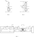
- FIGs. 3 and 4 respectively illustrate sensing circuits 1207 in accordance with the present disclosure.
- the sensing circuit 1207 may comprise a shunt resistor being arranged in series to the LED load 3.
- a shunt may refer to a device that creates a low-resistance path for electric current, to allow it to pass around another portion of the circuit.
- a (shunt) voltage 1206 being indicative of said load current will emerge across the shunt resistor R s .
- V shunt ILED ⁇ R s
- the sensing circuit 1207 may comprise a resistive voltage divider being arranged in parallel to the LED load 3.
- a voltage 1206 being indicative of the same will emerge across a portion of the (high-resistance) voltage divider.
- FIG. 5 illustrates a feedback path in accordance with the present disclosure.
- a sensing circuit 1207 of FIGs. 3 or 4 is arranged for providing a voltage 1206 being indicative of the controlled variable 1204 of the converter 1.
- the sensing circuit 1207 may comprise a low-pass filter 1209 for de-noising a magnitude of the voltage 1206.
- the sensing circuit 1207 may comprise an operational amplifier 1208 for amplifying the magnitude of the voltage 1206.
- VCO voltage-controlled oscillator
- V vco_out 2 MHz ⁇ 1 MHz 3.3 V ⁇ 0 V ⁇ ILED ⁇ R s ⁇ g op + 1 MHz
- a second transformer 1202, 1102 is provided for an inductive signal transfer of said oscillation signal 1103, 1203 from the secondary-side circuit 12 to the primary-side circuit 11.
- the oscillation signal 1103 may have an unipolar magnitude. e.g., alternating between 0V and +3.3V, in which case the oscillation signal 1103 may directly serve as the indication 1103' of the controlled variable 1204 of the converter 1.
- the oscillation signal 1103 may have a bipolar magnitude, e.g., alternating between - 3.3V and +3.3V.
- the converter 1 may further comprise a diode 1108 interposed between the second transformer 1102, 1202 and the control circuit 1107 for providing the (rectified) indication 1103' of the controlled variable 1204 of the converter 1.
- control circuit 1107 is arranged for providing the actuating variable 1106 of the converter 1 in accordance with the indication 1103', 1103 of the controlled variable 1204 of the converter 1 (and an indication 1103" of a reference variable of the converter 1).
- ILED 1 T Vsns _ in ⁇ 1 MHz R s ⁇ g op ⁇ 3.3 V ⁇ 0 V 2 MHz ⁇ 1 MHz
- ILED 0.5 ⁇ s , 3.3 ⁇ , 1 1
- ILED 0.667 ⁇ s , 3.3 ⁇ , 1 0.499
- ILED 1 ⁇ s , 3.3 ⁇ , 1 0
- ILED 0.5 ⁇ s , 3.3 ⁇ , 1 1
- the load current value can be calculated by the equations presented above. This calculation can be implemented within an ASIC or microcontroller in order to calculate the load current based on the measured period of the sensing signal 1103', V sns_in . The calculated load current then is the feedback / measurement value of the control loop.
- the control loop could also work with period (or frequency) values rather than load current values. In that case the target load current value needs to be converted into a target period (or frequency) value of the sensing signal. The control loop then would have to use that target value and compare it to the measured value.
- FIGs. 6 and 7 respectively illustrate example waveforms for different VCO output voltage ranges.
- the sensing circuit 1207 translates different levels of the load current 1204 into different levels of the voltages 1206, 1206' being indicative of the controlled variable 1204 of the converter 1.
- an output voltage 1203 of the VCO 1205 oscillates between 0V and +3.3V
- the output voltage 1203 of the VCO 1205 oscillates between -3.3V and +3.3V.
- the voltage is rectangular, but could be also e.g. sinusoidal.
- a low (high) load current 1204 and therefore a low (high) shunt voltage 1206 translates into a low (high) VCO input voltage 1206' and further into a low (high) frequency of the VCO output voltage 1203.
- the signals 1103 (oscillation signal) and 1103' have a same frequency, as the second transformer 1202, 1102 (and the diode 1108, if any) do/does not change the frequency.
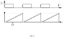
- FIG. 8 illustrates a measurement of an oscillation period of an indication 1103', 1103 of a controlled variable 1204 of an isolated converter 1 in accordance with the present disclosure.
- This measurement may be carried out in the control circuit 1107 (i.e., ASIC) by means of a counter. Whenever a rising edge of the input signal 1103', 1103 is detected, the current counter value is latched (i.e., stored), reset to zero, and incremented at each ASIC clock cycle (with period T clk ). The latched counter value is proportional to a duration of the oscillation period of the indication 1103', 1103 of the controlled variable 1204 and may thus be used to calculate the load current 1204.
Landscapes
- Engineering & Computer Science (AREA)
- Power Engineering (AREA)
- Dc-Dc Converters (AREA)
Abstract
Description
- The present disclosure relates to lighting technology, and more specifically to an isolated electric power converter for supplying a light emitting device (LED) load, as well as to an LED driver comprising such an isolated power converter. "Isolated" is to be understood as comprising an isolation barrier, typically a transformer.
- Exemplary isolated topologies of LED drivers/gears include half-bridge resonant converters, flyback converters, or buck (i.e., step-down) converters being located on a secondary side of an intermediate DC/DC stage.
- The driver's controller for regulation of a constant output current or a constant output voltage is usually arranged on a primary side with respect to the isolation barrier.
- Since a required sensing accuracy of e.g. +/-3% of the load current/voltage cannot be achieved by a primary-side sensing, there is a need for a secondary-side sensing and a feedback of the load current/voltage to the primary side. This can be done e.g. by a transformer (if the sensed signal is of AC type) or via optocoupler solutions.
- Transformer solutions have the drawback that they do not work if the signal that is to be sensed is of DC type (e.g. the DC output current flowing through the LED). Additionally they are expensive and need quite a lot of space.
- Optocoupler solutions have the drawback that the transfer characteristics of optocouplers are subject to large tolerances and temperature dependency.
- Depending on the solution the accuracy may be low and/or a cost may be high.
- In view of the above-mentioned drawbacks and limitations, the present disclosure seeks to achieve a secondary-side sensing of an output current (or voltage) at a reasonable price with acceptable accuracy.
- The objective is achieved by the embodiments as defined by the appended independent claims. Preferred embodiments are set forth in the dependent claims and in the following description and drawings.
- A first aspect of the present disclosure relates to an isolated power converter for supplying an LED load. The converter comprises a first transformer for an inductive power transfer from a primary-side circuit to a secondary-side circuit; and a second transformer for an inductive signal transfer of an oscillation signal from the secondary-side circuit to the primary-side circuit. The primary-side circuit comprises a switching circuit for intermittent power input from a direct-current, DC, power source of the converter in accordance with an actuating variable of the converter; and a control circuit for providing the actuating variable of the converter in accordance with an indication of a controlled variable of the converter and an indication of a reference variable of the converter. The secondary-side circuit comprises a voltage-controlled oscillator, VCO, for providing the oscillation signal having a frequency in accordance with a magnitude of a voltage being e.g. indicative of the controlled variable of the converter; and a sensing circuit for providing the voltage being indicative of the controlled variable of the converter.
- The frequency of the oscillation signal may be proportionate to the magnitude of the voltage.
- The indication of the controlled variable of the converter may be proportionate to the frequency of the oscillation signal.
- The indication of the controlled variable of the converter and the indication of the reference variable of the converter may respectively comprise one of: magnitude values, and frequency values.
- The sensing circuit may further comprise an operational amplifier upstream of the VCO.
- The sensing circuit may further comprise a low-pass filter upstream of the operational amplifier.
- The controlled variable of the converter may comprise a load voltage; and the sensing circuit may comprise a resistive voltage divider being arranged in parallel to the LED load.
- The controlled variable of the converter may comprise a load current; and the sensing circuit may comprise a shunt resistor being arranged in series to the LED load.
- The actuating variable of the converter may comprise a switching frequency.
- The control circuit may comprise a lookup table for providing the actuating variable of the converter in accordance with the frequency of the oscillation signal and a given type of the controlled variable of the converter.
- The oscillation signal may comprise one of: a square-wave signal, and a sine-wave signal.
- The oscillation signal may have an unipolar magnitude; or the oscillation signal may have a bipolar magnitude and the converter may further comprise a diode interposed between the second transformer and the control circuit.
- The converter may comprise a flyback converter; and the switching circuit may comprise a single switch.
- The converter may comprise a resonant converter; the switching circuit may comprise a half-bridge of series-connected switches being operable in alternation; and the primary-side circuit may further comprise a resonant tank circuit.
- A second aspect of the present disclosure relates to an LED driver, comprising an isolated power converter according to the first aspect or any of its implementations for supplying an LED load.
- The present disclosure provides a secondary-side output current (or voltage) sensing at a reasonable price with acceptable accuracy.
- The above-described aspects and implementations will now be explained with reference to the accompanying drawings, in which the same or similar reference numerals designate the same or similar elements.
- The features of these aspects and implementations may be combined with each other unless specifically stated otherwise.
- The drawings are to be regarded as being schematic representations, and elements illustrated in the drawings are not necessarily shown to scale. Rather, the various elements are represented such that their function and general purpose become apparent to those skilled in the art.
- FIG. 1
- illustrates a block diagram of an exemplary isolated LED driver 2 in accordance with the present disclosure;
- FIG. 2
- illustrates a block diagram of an exemplary control loop of an isolated converter 1 in accordance with the present disclosure;
- FIGs. 3 and 4
- respectively illustrate
sensing circuits 1207 in accordance with the present disclosure; - FIG. 5
- illustrates a feedback path in accordance with the present disclosure;
- FIGs. 6 and 7
- respectively illustrate example waveforms for different VCO output voltage ranges; and
- FIG. 8
- illustrates a measurement of an oscillation period of an
indication 1103', 1103 of a controlledvariable 1204 of an isolated converter 1 in accordance with the present disclosure; -
FIG. 1 illustrates a block diagram of an exemplary isolated LED driver 2 in accordance with the present disclosure. - The LED driver 2 comprises an isolated power converter 1 according to the first aspect of the present disclosure or any of its implementations. The isolated power converter 1 is designed for supplying an
LED load 3, and with respect to its isolation barrier includes a primary-side circuit 11 and a secondary-side circuit 12. - Starting at a power inlet, the converter 1 may comprise a rectifier and
filter circuit 1110 for rectifying and EMI-filtering of an alternating-current (AC)mains voltage 1109. - Progressing along a power path, the converter 1 may further comprise a direct-current (DC)
power source 1105, such as a DC/DC power factor correction (PFC) stage based on a boost topology, for providing aconstant bus voltage 1112, Vbus. - Further along the power path, a primary-
side circuit 11 of the converter 1 comprises aswitching circuit 1104 for intermittent power input from theDC power source 1105 of the converter 1 in accordance with anactuating variable 1106 of the converter 1. - The
actuating variable 1106 of the converter 1 may comprise a switching frequency. - As shown in
FIG. 1 , the converter 1 may comprise a resonant converter 1. In that case, theswitching circuit 1104 may comprise a half-bridge of series-connected switches being operable in alternation; and the primary-side circuit 11 may further comprise a resonant tank circuit 1104' such as an LCC circuit topology (for a current source) or an LLC circuit topology (for a voltage source) further along the power path. - Alternatively to the resonant topology of
FIG. 1 , the converter 1 may comprise a flyback converter 1, in which case theswitching circuit 1104 may comprise a single switch and the primary-side circuit 11 may further comprise an inductor 1104' further along the power path. - Irrespective of the actual topology, the converter 1 thus comprises a
first transformer side circuit 11 to the secondary-side circuit 12 of the converter 1. - Further along the power path, the secondary-
side circuit 12 may further comprise a further rectifier andfilter circuit 1210 for rectifying and filtering the output current 1204 being fed to theLED load 3. - In the case of output current regulation, the output current 1204 flowing through the
LED load 3 may be sensed and theactuating variable 1106 of the converter 1 may be provided using an approach as will be described in the following. - The converter 1 further comprises a
control circuit 1107, such as an application-specific integrated circuit (ASIC) or a microcontroller (µC), for providing theactuating variable 1106 of the converter 1 in accordance with anindication 1103', 1103 of a controlled variable 1204 of the converter 1 and anindication 1103" (Fig. 2 ) of a reference variable of the converter 1. - The
indication 1103', 1103 of the controlledvariable 1204 of the converter 1 and theindication 1103" of the reference variable of the converter 1 may respectively comprise one of: magnitude values, and frequency values. - The
indication 1103', 1103 of the controlledvariable 1204 of the converter 1 may be proportionate to a frequency of anoscillation signal - Regressing along a feedback path, the converter 1 further comprises a
second transformer oscillation signal side circuit 12 to the primary-side circuit 11. In particular, thesecond transformer oscillation signal - The
oscillation signal - Further against the feedback path, the secondary-
side circuit 12 further comprises a voltage-controlled oscillator,VCO 1205, for providing theoscillation signal voltage 1206, 1206' being indicative of the controlledvariable 1204 of the converter 1. In particular, the frequency of theoscillation signal voltage 1206, 1206' being indicative of the controlledvariable 1204 of the converter 1. - Further against the feedback path, the secondary-
side circuit 12 further comprises asensing circuit 1207 for providing thevoltage 1206, 1206' being indicative of the controlledvariable 1204 of the converter 1. - Off the power and feedback paths, the
primary side 11 of the converter 1 may further comprise, in accordance withFIG. 1 , amicrocontroller 1113, a low-voltage power supply (LVPS)stage 1114 for theswitching circuit 1104,control circuit 1107 and themicrocontroller 1113, aninterface circuit 1115 for communications between themicrocontroller 1113 and alighting control bus 1116 such as a Digital Addressable Lighting Interface (DALI) bus, as well as a mains voltage monitoring circuit 1117 for mains voltage monitoring by themicrocontroller 1113. -
FIG. 2 illustrates a block diagram of an exemplary control loop of an isolated converter 1 in accordance with the present disclosure. - The controlled
variable 1204 of the converter 1 may comprise a load voltage (across the LED load 3) or a load current (through the LED load 3). - The feedback loop comprises a
sensing circuit 1207 for providing avoltage 1206, 1206' being indicative of the controlledvariable 1204 of the converter 1. - The feedback loop further comprises further elements discussed in connection with
FIG. 5 below and an analog/digital converter (ADC) 1120 for providing anindication 1103', 1103 of the controlledvariable 1204 of the isolated converter 1. - As previously mentioned, the
control circuit 1107 is designed for providing theactuating variable 1106 of the converter 1 in accordance with theindication 1103', 1103 of the controlledvariable 1204 of the converter 1 (i.e., the sensed value) and theindication 1103" of a reference variable of the converter 1 (i.e., the target value). - The feedback loop may further comprise a proportional-integral, PI,
controller 1118 for providing a drive control signal in accordance with an error of thetarget value 1103" and the sensed value 1103'. - The feedback loop may further comprise a
driver circuit 1119 for actuating the system under control (i.e., plant) 1104, 1104', 1101, 1201, 1210 (seeFIG. 1 ) in accordance with the drive control signal provided by thePI controller 1118. - According to
FIG. 1 , the system under control (i.e., plant) 1104, 1104', 1101, 1201, 1210 comprises theswitching circuit 1104, the resonant tank circuit (or inductor) 1104' and thefirst transformer filter circuit 1210. - The
switching circuit 1104 is designed for intermittent power input from theDC power source 1105 of the converter 1 in accordance with theactuating variable 1106 of the converter 1, which may comprise a switching frequency of theswitching circuit 1104. - For practical reasons, the
control circuit 1107 may comprise a lookup table for providing theactuating variable 1106 of the converter 1 in accordance with the frequency of theoscillation signal - The
switching circuit 1104 may thus be operated at this frequency/period (with a constant duty cycle of e.g. 50%), and a load current or load voltage equivalent to the target value will emerge. -
FIGs. 3 and 4 respectively illustratesensing circuits 1207 in accordance with the present disclosure. - On the one hand, if the controlled
variable 1204 of the converter 1 comprises a load current as shown inFIG. 3 , then thesensing circuit 1207 may comprise a shunt resistor being arranged in series to theLED load 3. - As used herein, a shunt may refer to a device that creates a low-resistance path for electric current, to allow it to pass around another portion of the circuit.
- In response to the load current (i.e., controlled variable) 1204, ILED , a (shunt)
voltage 1206 being indicative of said load current will emerge across the shunt resistor Rs . - The
shunt voltage 1206, Vshunt may be given as follows:
- On the other hand, if the controlled
variable 1204 of the converter 1 comprises a load voltage, then thesensing circuit 1207 may comprise a resistive voltage divider being arranged in parallel to theLED load 3. - In response to the load voltage (i.e., controlled variable) 1204, a
voltage 1206 being indicative of the same will emerge across a portion of the (high-resistance) voltage divider. -
FIG. 5 illustrates a feedback path in accordance with the present disclosure. - At a beginning of the feedback path, a
sensing circuit 1207 ofFIGs. 3 or 4 is arranged for providing avoltage 1206 being indicative of the controlledvariable 1204 of the converter 1. - Further along the feedback path, the
sensing circuit 1207 may comprise a low-pass filter 1209 for de-noising a magnitude of thevoltage 1206. - Further along the feedback path, the
sensing circuit 1207 may comprise anoperational amplifier 1208 for amplifying the magnitude of thevoltage 1206. - Given the gain gop of the operational amplifier, the VCO input voltage 1206', Vvco_in may be calculated as follows:

- Further along the feedback path, a voltage-controlled oscillator (VCO) 1205 is arranged for providing an
oscillation signal voltage 1206, 1206' being indicative of the controlledvariable 1204 of the converter 1. - For example, the transfer characteristics of the
VCO 1205 may be described as follows:
- Combining the equations above, the frequency of the
VCO output voltage 1203, Vvco_out may be calculated as follows:
- Further along the feedback path, a
second transformer oscillation signal side circuit 12 to the primary-side circuit 11. - The
oscillation signal 1103 may have an unipolar magnitude. e.g., alternating between 0V and +3.3V, in which case theoscillation signal 1103 may directly serve as the indication 1103' of the controlledvariable 1204 of the converter 1. - Alternatively, the
oscillation signal 1103 may have a bipolar magnitude, e.g., alternating between - 3.3V and +3.3V. As negative voltages cannot be fed to the control circuit (i.e., ASIC) 1107, the converter 1 may further comprise adiode 1108 interposed between thesecond transformer control circuit 1107 for providing the (rectified) indication 1103' of the controlledvariable 1204 of the converter 1. - As the
second transformer 
- At an ending of the feedback path, the
control circuit 1107 is arranged for providing theactuating variable 1106 of the converter 1 in accordance with theindication 1103', 1103 of the controlledvariable 1204 of the converter 1 (and anindication 1103" of a reference variable of the converter 1). - Combining the equations above, the oscillation period T Vsns_in of the sensing signal 1103', Vsns_in may be calculated as follows:

- Solving this equation for ILED yields:

- Given Rs = 3,3Ω and gop = 1 the following exemplary values may be obtained for ILED (depending on the period TVsns_in of the sensing signal):


- As can be seen, the load current value can be calculated by the equations presented above. This calculation can be implemented within an ASIC or microcontroller in order to calculate the load current based on the measured period of the sensing signal 1103', Vsns_in. The calculated load current then is the feedback / measurement value of the control loop. Clearly, the control loop could also work with period (or frequency) values rather than load current values. In that case the target load current value needs to be converted into a target period (or frequency) value of the sensing signal. The control loop then would have to use that target value and compare it to the measured value.
-
FIGs. 6 and 7 respectively illustrate example waveforms for different VCO output voltage ranges. - Both relate to the scenario of
FIG. 3 wherein the controlledvariable 1204 of the converter 1 comprises a load current. - The
sensing circuit 1207 translates different levels of the load current 1204 into different levels of thevoltages 1206, 1206' being indicative of the controlledvariable 1204 of the converter 1. - In
FIG. 6 anoutput voltage 1203 of theVCO 1205 oscillates between 0V and +3.3V, whereas inFIG. 7 theoutput voltage 1203 of theVCO 1205 oscillates between -3.3V and +3.3V. In both examples the voltage is rectangular, but could be also e.g. sinusoidal. - It applies to both FIGs. that a low (high) load current 1204 and therefore a low (high)
shunt voltage 1206 translates into a low (high) VCO input voltage 1206' and further into a low (high) frequency of theVCO output voltage 1203. As can be seen, the signals 1103 (oscillation signal) and 1103' (the indication of the controlledvariable 1204 of the converter 1) have a same frequency, as thesecond transformer 1202, 1102 (and thediode 1108, if any) do/does not change the frequency. -
FIG. 8 illustrates a measurement of an oscillation period of anindication 1103', 1103 of a controlled variable 1204 of an isolated converter 1 in accordance with the present disclosure. - This measurement may be carried out in the control circuit 1107 (i.e., ASIC) by means of a counter. Whenever a rising edge of the
input signal 1103', 1103 is detected, the current counter value is latched (i.e., stored), reset to zero, and incremented at each ASIC clock cycle (with period Tclk). The latched counter value is proportional to a duration of the oscillation period of theindication 1103', 1103 of the controlled variable 1204 and may thus be used to calculate the load current 1204. - Similar considerations apply in case of the scenario of
FIG. 4 wherein the controlledvariable 1204 of the converter 1 comprises a load voltage.
Claims (15)
- An isolated power converter (1) for supplying an LED load (3), the converter (1) comprisinga first transformer (1101, 1201) for an inductive power transfer from a primary-side circuit (11) to a secondary-side circuit (12);a second transformer (1102, 1202) for an inductive signal transfer of an oscillation signal (1203, 1103) from the secondary-side circuit (12) to the primary-side circuit (11);
the primary-side circuit (11) comprisinga switching circuit (1104) for intermittent power input from a direct-current, DC, power source (1105) of the converter (1) in accordance with an actuating variable (1106) of the converter (1); anda control circuit (1107) for providing the actuating variable (1106) of the converter (1) in accordance with an indication (1103', 1103) of a controlled variable (1204) of the converter (1) and an indication (1103") of a reference variable of the converter (1);
the secondary-side circuit (12) comprisinga voltage-controlled oscillator, VCO (1205), for providing the oscillation signal (1203, 1103) having a frequency in accordance with a magnitude of a voltage (1206, 1206') being indicative of the controlled variable (1204) of the converter (1); anda sensing circuit (1207) for providing the voltage (1206, 1206') being indicative of the controlled variable (1204) of the converter (1). - The converter (1) of claim 1,
the frequency of the oscillation signal (1203, 1103) being proportionate to the magnitude of the voltage (1206, 1206') being indicative of the controlled variable (1204) of the converter (1). - The converter (1) of claim 1 or claim 2,
the indication (1103', 1103) of the controlled variable (1204) of the converter (1) being proportionate to the frequency of the oscillation signal (1203, 1103). - The converter (1) of any one of the claims 1 to 3,
the indication (1103', 1103) of the controlled variable (1204) of the converter (1) and the indication (1103") of the reference variable of the converter (1) respectively comprising one of: magnitude values, and frequency values. - The converter (1) of any one of the preceding claims,
the sensing circuit (1207) further comprising an operational amplifier (1208) upstream of the VCO (1205). - The converter (1) of claim 5,
the sensing circuit (1207) further comprising a low-pass filter (1209) upstream of the operational amplifier (1208). - The converter (1) of any one of the claims 1 to 6,the controlled variable (1204) of the converter (1) comprising a load voltage;the sensing circuit (1207) comprising a resistive voltage divider being arranged in parallel to the LED load (3).
- The converter (1) of any one of the claims 1 to 6,the controlled variable (1204) of the converter (1) comprising a load current;the sensing circuit (1207) comprising a shunt resistor being arranged in series to the LED load (3).
- The converter (1) of any one of the preceding claims,
the actuating variable (1106) of the converter (1) comprising a switching frequency. - The converter (1) of any one of the preceding claims,the control circuit (1107) comprising a lookup table for providing the actuating variable (1106) ofthe converter (1) in accordance with the frequency of the oscillation signal (1203, 1103) and a given type of the controlled variable (1204) of the converter (1).
- The converter (1) of any one of the preceding claims,
the oscillation signal (1203, 1103) comprising one of: a square-wave signal, and a sine-wave signal. - The converter (1) of any one of the preceding claims,the oscillation signal (1203, 1103) having an unipolar magnitude; orthe oscillation signal (1203, 1103) having a bipolar magnitude and the converter (1) further comprising a diode (1108) interposed between the second transformer (1102, 1202) and the control circuit (1107).
- The converter (1) of any one of the claims 1 to 12,the converter (1) comprising a flyback converter (1);the switching circuit (1104) comprising a single switch; andthe primary-side circuit (11) further comprising an inductor (1104').
- The converter (1) of any one of the claims 1 to 12,the converter (1) comprising a resonant converter (1);the switching circuit (1104) comprising a half-bridge of series-connected switches being operable in alternation; andthe primary-side circuit (11) further comprising a resonant tank circuit (1104').
- An LED driver (2), comprising
an isolated power converter (1) of any one of the preceding claims for supplying an LED load (3) at output terminals of the LED driver.
Priority Applications (1)
| Application Number | Priority Date | Filing Date | Title |
|---|---|---|---|
| EP22206008.9A EP4369587A1 (en) | 2022-11-08 | 2022-11-08 | Load current/voltage sensing for isolated power converter |
Applications Claiming Priority (1)
| Application Number | Priority Date | Filing Date | Title |
|---|---|---|---|
| EP22206008.9A EP4369587A1 (en) | 2022-11-08 | 2022-11-08 | Load current/voltage sensing for isolated power converter |
Publications (1)
| Publication Number | Publication Date |
|---|---|
| EP4369587A1 true EP4369587A1 (en) | 2024-05-15 |
Family
ID=84330373
Family Applications (1)
| Application Number | Title | Priority Date | Filing Date |
|---|---|---|---|
| EP22206008.9A Pending EP4369587A1 (en) | 2022-11-08 | 2022-11-08 | Load current/voltage sensing for isolated power converter |
Country Status (1)
| Country | Link |
|---|---|
| EP (1) | EP4369587A1 (en) |
Citations (4)
| Publication number | Priority date | Publication date | Assignee | Title |
|---|---|---|---|---|
| EP0851565A2 (en) * | 1993-06-14 | 1998-07-01 | Vlt Corporation | Power converter configuration control and construction |
| US20160359419A1 (en) * | 2014-12-07 | 2016-12-08 | Alpha And Omega Semiconductor (Cayman) Ltd. | Voltage converter |
| EP3244696A1 (en) * | 2016-05-12 | 2017-11-15 | Helvar Oy Ab | Method and apparatus for providing feedback in an isolated operating device for lighting |
| US20200083874A1 (en) * | 2018-09-07 | 2020-03-12 | Analog Devices Global Unlimited Company | Multi-mode feedback control through digital isolator |
-
2022
- 2022-11-08 EP EP22206008.9A patent/EP4369587A1/en active Pending
Patent Citations (4)
| Publication number | Priority date | Publication date | Assignee | Title |
|---|---|---|---|---|
| EP0851565A2 (en) * | 1993-06-14 | 1998-07-01 | Vlt Corporation | Power converter configuration control and construction |
| US20160359419A1 (en) * | 2014-12-07 | 2016-12-08 | Alpha And Omega Semiconductor (Cayman) Ltd. | Voltage converter |
| EP3244696A1 (en) * | 2016-05-12 | 2017-11-15 | Helvar Oy Ab | Method and apparatus for providing feedback in an isolated operating device for lighting |
| US20200083874A1 (en) * | 2018-09-07 | 2020-03-12 | Analog Devices Global Unlimited Company | Multi-mode feedback control through digital isolator |
Similar Documents
| Publication | Publication Date | Title |
|---|---|---|
| US10326377B1 (en) | Circuit and method for indirect primary-side load current sensing in an isolated power supply | |
| JP6673992B2 (en) | Power regulator | |
| TWI566637B (en) | A cascade boost and inverting buck converter with independent control | |
| US8670255B2 (en) | Utilization of a multifunctional pin combining voltage sensing and zero current detection to control a switched-mode power converter | |
| US8125805B1 (en) | Switch-mode converter operating in a hybrid discontinuous conduction mode (DCM)/continuous conduction mode (CCM) that uses double or more pulses in a switching period | |
| CN103904920B (en) | Master inductive output electric current is adjusted | |
| CN102573218B (en) | light emitting diode driver and control method | |
| EP2690774B1 (en) | Voltage sensing in isolated DC/DC converters | |
| US20170280523A1 (en) | Single-stage multi-string led driver with dimming | |
| CN103023352B (en) | An AC-DC Power Converter | |
| CN102355136B (en) | Control method and control circuit for controlling output current of converter | |
| US10658932B2 (en) | Power control circuit | |
| US20250096689A1 (en) | A switched converter | |
| JP2011152017A (en) | Switching power supply device | |
| US20150162833A1 (en) | Switching shunt regulator circuits | |
| CN115053633B (en) | Resonant inverter and conversion method | |
| TWI533745B (en) | Light source driving circuit, controller and method for controlling power converter | |
| WO2016107728A1 (en) | A controllable driver and drive method | |
| CN105591555B (en) | The indirect adjusting of output electric current in power converter | |
| JP5424804B2 (en) | Interleave type switching power supply | |
| US20040263096A1 (en) | Method for operating at least one low-pressure discharge lamp and operating device for at least one low-pressure discharge lamp | |
| KR101609726B1 (en) | Control circuit of switching rectifier with high power factor | |
| CN204168555U (en) | Power circuit and lighting device | |
| US9748849B2 (en) | Power supply | |
| EP3407682B1 (en) | Converter device |
Legal Events
| Date | Code | Title | Description |
|---|---|---|---|
| PUAI | Public reference made under article 153(3) epc to a published international application that has entered the european phase |
Free format text: ORIGINAL CODE: 0009012 |
|
| STAA | Information on the status of an ep patent application or granted ep patent |
Free format text: STATUS: THE APPLICATION HAS BEEN PUBLISHED |
|
| AK | Designated contracting states |
Kind code of ref document: A1 Designated state(s): AL AT BE BG CH CY CZ DE DK EE ES FI FR GB GR HR HU IE IS IT LI LT LU LV MC ME MK MT NL NO PL PT RO RS SE SI SK SM TR |
|
| STAA | Information on the status of an ep patent application or granted ep patent |
Free format text: STATUS: REQUEST FOR EXAMINATION WAS MADE |
|
| 17P | Request for examination filed |
Effective date: 20240821 |
|
| RBV | Designated contracting states (corrected) |
Designated state(s): AL AT BE BG CH CY CZ DE DK EE ES FI FR GB GR HR HU IE IS IT LI LT LU LV MC ME MK MT NL NO PL PT RO RS SE SI SK SM TR |