EP4369536A2 - Polarized/lensed back-side emitting (bse) vertical-cavity surface-emitting laser (vcsel) - Google Patents
Polarized/lensed back-side emitting (bse) vertical-cavity surface-emitting laser (vcsel) Download PDFInfo
- Publication number
- EP4369536A2 EP4369536A2 EP23204680.5A EP23204680A EP4369536A2 EP 4369536 A2 EP4369536 A2 EP 4369536A2 EP 23204680 A EP23204680 A EP 23204680A EP 4369536 A2 EP4369536 A2 EP 4369536A2
- Authority
- EP
- European Patent Office
- Prior art keywords
- gaas
- vcsel
- mirrors
- grating
- vcsel structure
- Prior art date
- Legal status (The legal status is an assumption and is not a legal conclusion. Google has not performed a legal analysis and makes no representation as to the accuracy of the status listed.)
- Pending
Links
Images

Classifications
-
- H—ELECTRICITY
- H01—ELECTRIC ELEMENTS
- H01S—DEVICES USING THE PROCESS OF LIGHT AMPLIFICATION BY STIMULATED EMISSION OF RADIATION [LASER] TO AMPLIFY OR GENERATE LIGHT; DEVICES USING STIMULATED EMISSION OF ELECTROMAGNETIC RADIATION IN WAVE RANGES OTHER THAN OPTICAL
- H01S5/00—Semiconductor lasers
- H01S5/10—Construction or shape of the optical resonator, e.g. extended or external cavity, coupled cavities, bent-guide, varying width, thickness or composition of the active region
- H01S5/18—Surface-emitting [SE] lasers, e.g. having both horizontal and vertical cavities
- H01S5/183—Surface-emitting [SE] lasers, e.g. having both horizontal and vertical cavities having only vertical cavities, e.g. vertical cavity surface-emitting lasers [VCSEL]
- H01S5/18305—Surface-emitting [SE] lasers, e.g. having both horizontal and vertical cavities having only vertical cavities, e.g. vertical cavity surface-emitting lasers [VCSEL] with emission through the substrate, i.e. bottom emission
-
- H—ELECTRICITY
- H01—ELECTRIC ELEMENTS
- H01S—DEVICES USING THE PROCESS OF LIGHT AMPLIFICATION BY STIMULATED EMISSION OF RADIATION [LASER] TO AMPLIFY OR GENERATE LIGHT; DEVICES USING STIMULATED EMISSION OF ELECTROMAGNETIC RADIATION IN WAVE RANGES OTHER THAN OPTICAL
- H01S5/00—Semiconductor lasers
- H01S5/10—Construction or shape of the optical resonator, e.g. extended or external cavity, coupled cavities, bent-guide, varying width, thickness or composition of the active region
- H01S5/18—Surface-emitting [SE] lasers, e.g. having both horizontal and vertical cavities
- H01S5/183—Surface-emitting [SE] lasers, e.g. having both horizontal and vertical cavities having only vertical cavities, e.g. vertical cavity surface-emitting lasers [VCSEL]
- H01S5/18308—Surface-emitting [SE] lasers, e.g. having both horizontal and vertical cavities having only vertical cavities, e.g. vertical cavity surface-emitting lasers [VCSEL] having a special structure for lateral current or light confinement
- H01S5/18319—Surface-emitting [SE] lasers, e.g. having both horizontal and vertical cavities having only vertical cavities, e.g. vertical cavity surface-emitting lasers [VCSEL] having a special structure for lateral current or light confinement comprising a periodical structure in lateral directions
-
- H—ELECTRICITY
- H01—ELECTRIC ELEMENTS
- H01S—DEVICES USING THE PROCESS OF LIGHT AMPLIFICATION BY STIMULATED EMISSION OF RADIATION [LASER] TO AMPLIFY OR GENERATE LIGHT; DEVICES USING STIMULATED EMISSION OF ELECTROMAGNETIC RADIATION IN WAVE RANGES OTHER THAN OPTICAL
- H01S5/00—Semiconductor lasers
- H01S5/10—Construction or shape of the optical resonator, e.g. extended or external cavity, coupled cavities, bent-guide, varying width, thickness or composition of the active region
- H01S5/18—Surface-emitting [SE] lasers, e.g. having both horizontal and vertical cavities
- H01S5/183—Surface-emitting [SE] lasers, e.g. having both horizontal and vertical cavities having only vertical cavities, e.g. vertical cavity surface-emitting lasers [VCSEL]
- H01S5/18355—Surface-emitting [SE] lasers, e.g. having both horizontal and vertical cavities having only vertical cavities, e.g. vertical cavity surface-emitting lasers [VCSEL] having a defined polarisation
-
- H—ELECTRICITY
- H01—ELECTRIC ELEMENTS
- H01S—DEVICES USING THE PROCESS OF LIGHT AMPLIFICATION BY STIMULATED EMISSION OF RADIATION [LASER] TO AMPLIFY OR GENERATE LIGHT; DEVICES USING STIMULATED EMISSION OF ELECTROMAGNETIC RADIATION IN WAVE RANGES OTHER THAN OPTICAL
- H01S5/00—Semiconductor lasers
- H01S5/10—Construction or shape of the optical resonator, e.g. extended or external cavity, coupled cavities, bent-guide, varying width, thickness or composition of the active region
- H01S5/18—Surface-emitting [SE] lasers, e.g. having both horizontal and vertical cavities
- H01S5/183—Surface-emitting [SE] lasers, e.g. having both horizontal and vertical cavities having only vertical cavities, e.g. vertical cavity surface-emitting lasers [VCSEL]
- H01S5/18361—Structure of the reflectors, e.g. hybrid mirrors
- H01S5/18369—Structure of the reflectors, e.g. hybrid mirrors based on dielectric materials
-
- H—ELECTRICITY
- H01—ELECTRIC ELEMENTS
- H01S—DEVICES USING THE PROCESS OF LIGHT AMPLIFICATION BY STIMULATED EMISSION OF RADIATION [LASER] TO AMPLIFY OR GENERATE LIGHT; DEVICES USING STIMULATED EMISSION OF ELECTROMAGNETIC RADIATION IN WAVE RANGES OTHER THAN OPTICAL
- H01S5/00—Semiconductor lasers
- H01S5/10—Construction or shape of the optical resonator, e.g. extended or external cavity, coupled cavities, bent-guide, varying width, thickness or composition of the active region
- H01S5/18—Surface-emitting [SE] lasers, e.g. having both horizontal and vertical cavities
- H01S5/183—Surface-emitting [SE] lasers, e.g. having both horizontal and vertical cavities having only vertical cavities, e.g. vertical cavity surface-emitting lasers [VCSEL]
- H01S5/18361—Structure of the reflectors, e.g. hybrid mirrors
- H01S5/18377—Structure of the reflectors, e.g. hybrid mirrors comprising layers of different kind of materials, e.g. combinations of semiconducting with dielectric or metallic layers
-
- H—ELECTRICITY
- H01—ELECTRIC ELEMENTS
- H01S—DEVICES USING THE PROCESS OF LIGHT AMPLIFICATION BY STIMULATED EMISSION OF RADIATION [LASER] TO AMPLIFY OR GENERATE LIGHT; DEVICES USING STIMULATED EMISSION OF ELECTROMAGNETIC RADIATION IN WAVE RANGES OTHER THAN OPTICAL
- H01S5/00—Semiconductor lasers
- H01S5/10—Construction or shape of the optical resonator, e.g. extended or external cavity, coupled cavities, bent-guide, varying width, thickness or composition of the active region
- H01S5/18—Surface-emitting [SE] lasers, e.g. having both horizontal and vertical cavities
- H01S5/183—Surface-emitting [SE] lasers, e.g. having both horizontal and vertical cavities having only vertical cavities, e.g. vertical cavity surface-emitting lasers [VCSEL]
- H01S5/18361—Structure of the reflectors, e.g. hybrid mirrors
- H01S5/1838—Reflector bonded by wafer fusion or by an intermediate compound
-
- H—ELECTRICITY
- H01—ELECTRIC ELEMENTS
- H01S—DEVICES USING THE PROCESS OF LIGHT AMPLIFICATION BY STIMULATED EMISSION OF RADIATION [LASER] TO AMPLIFY OR GENERATE LIGHT; DEVICES USING STIMULATED EMISSION OF ELECTROMAGNETIC RADIATION IN WAVE RANGES OTHER THAN OPTICAL
- H01S5/00—Semiconductor lasers
- H01S5/02—Structural details or components not essential to laser action
- H01S5/0206—Substrates, e.g. growth, shape, material, removal or bonding
- H01S5/0208—Semi-insulating substrates
-
- H—ELECTRICITY
- H01—ELECTRIC ELEMENTS
- H01S—DEVICES USING THE PROCESS OF LIGHT AMPLIFICATION BY STIMULATED EMISSION OF RADIATION [LASER] TO AMPLIFY OR GENERATE LIGHT; DEVICES USING STIMULATED EMISSION OF ELECTROMAGNETIC RADIATION IN WAVE RANGES OTHER THAN OPTICAL
- H01S5/00—Semiconductor lasers
- H01S5/10—Construction or shape of the optical resonator, e.g. extended or external cavity, coupled cavities, bent-guide, varying width, thickness or composition of the active region
- H01S5/18—Surface-emitting [SE] lasers, e.g. having both horizontal and vertical cavities
- H01S5/183—Surface-emitting [SE] lasers, e.g. having both horizontal and vertical cavities having only vertical cavities, e.g. vertical cavity surface-emitting lasers [VCSEL]
- H01S5/18386—Details of the emission surface for influencing the near- or far-field, e.g. a grating on the surface
-
- H—ELECTRICITY
- H01—ELECTRIC ELEMENTS
- H01S—DEVICES USING THE PROCESS OF LIGHT AMPLIFICATION BY STIMULATED EMISSION OF RADIATION [LASER] TO AMPLIFY OR GENERATE LIGHT; DEVICES USING STIMULATED EMISSION OF ELECTROMAGNETIC RADIATION IN WAVE RANGES OTHER THAN OPTICAL
- H01S5/00—Semiconductor lasers
- H01S5/10—Construction or shape of the optical resonator, e.g. extended or external cavity, coupled cavities, bent-guide, varying width, thickness or composition of the active region
- H01S5/18—Surface-emitting [SE] lasers, e.g. having both horizontal and vertical cavities
- H01S5/183—Surface-emitting [SE] lasers, e.g. having both horizontal and vertical cavities having only vertical cavities, e.g. vertical cavity surface-emitting lasers [VCSEL]
- H01S5/18386—Details of the emission surface for influencing the near- or far-field, e.g. a grating on the surface
- H01S5/18388—Lenses
-
- H—ELECTRICITY
- H01—ELECTRIC ELEMENTS
- H01S—DEVICES USING THE PROCESS OF LIGHT AMPLIFICATION BY STIMULATED EMISSION OF RADIATION [LASER] TO AMPLIFY OR GENERATE LIGHT; DEVICES USING STIMULATED EMISSION OF ELECTROMAGNETIC RADIATION IN WAVE RANGES OTHER THAN OPTICAL
- H01S5/00—Semiconductor lasers
- H01S5/40—Arrangement of two or more semiconductor lasers, not provided for in groups H01S5/02 - H01S5/30
- H01S5/42—Arrays of surface emitting lasers
- H01S5/423—Arrays of surface emitting lasers having a vertical cavity
Definitions
- BSE VCSEL back-side emitting, vertical-cavity surface-emitting laser
- a vertical-cavity surface-emitting laser is a type of semiconductor laser diode with laser beam emission perpendicular from the top surface, contrary to conventional edge-emitting semiconductor lasers which emit from surfaces formed by cleaving the individual chip out of a wafer.
- VCSELs are used in various laser products, including computer mice, fiber optic communications, laser printers, Face ID, and smart glasses.
- BSE back-side emitting
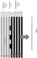
- FIG. 1 illustrates an example polarized/lensed BSE VCSEL structure, with dielectric mirrors, in accordance with various example implementations of this disclosure.
- the non-emitting side, of the BSE VCSEL structure in FIG. 1 comprises dielectric mirrors 101.
- the dielectric mirrors 101 may comprise alternating quarter wavelength layers of Si and SiN.
- the emitting side, of the BSE VCSEL structure in FIG. 1 comprises GaAs/AIGaAs mirrors 103.
- the GaAs/AIGaAs mirrors 103 may be plasma enhanced chemical vapor deposited (PECVD) alternating quarter wavelength layers of GaAs and AlGaAs. There may be more layers in the GaAs/AIGaAs mirrors 103 than the dielectric mirrors 101.
- PECVD plasma enhanced chemical vapor deposited
- the dielectric mirrors 101 and the GaAs/AIGaAs mirrors 103 are separated by a grating 105 operable to polarize incident waves of the BSE VCSEL.
- the grating 105 may comprise areas of GaAs.
- An optical emitter such as a lens 107, a focusing metasurface or diffractive optical element (DOE), is located on the emitting side. The surface of the emitter on the emitting side may be covered in an anti-reflective (AR) coating layer.
- AR anti-reflective
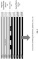
- FIG. 2 illustrates an example polarized/lensed BSE VCSEL structure, with regrown DBR, in accordance with various example implementations of this disclosure.
- the non-emitting side, of the BSE VCSEL structure in FIG. 2 comprises regrown GaAs/AIGaAs mirrors 201.
- the regrown layers immediately above the grating layer 105 may not be planar, which may aid the polarization locking.
- the emitting side, of the BSE VCSEL structure in FIG. 2 comprises GaAs/AIGaAs mirrors 103.
- the GaAs/AIGaAs mirrors 103 may be plasma enhanced chemical vapor deposited (PECVD) alternating quarter wavelength layers of GaAs and AlGaAs. There may be more layers in the GaAs/AIGaAs mirrors 103 than the dielectric mirrors 101.
- PECVD plasma enhanced chemical vapor deposited
- the dielectric mirrors 101 and the GaAs/AIGaAs mirrors 103 are separated by a grating 105 operable to polarize incident waves of the BSE VCSEL.
- the grating 105 may comprise areas of GaAs.
- An optical emitter, such as a lens 107, a focusing metasurface or a DOE, is located on the emitting side. The surface of the emitter on the emitting side may be covered in an AR coating layer.
- FIG. 3 illustrates an example polarized/lensed BSE VCSEL structure, with wafer bonding, in accordance with various example implementations of this disclosure.
- the BSE VCSEL structure in FIG. 5 comprises a lens 501, a semi-insulating (SI) GaAs substrate 503, a current spreading layer 505, a first DBR 507, a cladding layer 509, a linear grating 511, one or more quantum wells (QWs) 513, a second DBR 515 and a contact layer 517. All the layers in the stack, with an exception of the SI GaAs substrate 503, may be doped to support current injection into the active region.
- SI GaAs substrate 503 may be doped to support current injection into the active region.
- the linear GaAs/Air polarizing grating 511 operable to polarize incident waves of the BSE VCSEL, is inserted near the VCSEL cavity 513 by wafer bonding 519.
- Optics 501 operable to collimate incident waves of the BSE VCSEL, are located on the emitting side 107 of the substrate 503.
- An optical emitter such as a lens, metasurface, or DOE, is located on the emitting side. The surface of the emitter on the emitting side may be covered in an AR coating layer.
- the present method and/or system may be realized in hardware, software, or a combination of hardware and software.
- the present methods and/or systems may be realized in a centralized fashion in at least one computing system, or in a distributed fashion where different elements are spread across several interconnected computing systems. Any kind of computing system or other apparatus adapted for carrying out the methods described herein is suited.
- a typical implementation may comprise one or more application specific integrated circuit (ASIC), one or more field programmable gate array (FPGA), and/or one or more processor (e.g., x86, x64, ARM, PIC, and/or any other suitable processor architecture) and associated supporting circuitry (e.g., storage, DRAM, FLASH, bus interface circuits, etc.).
- ASIC application specific integrated circuit
- FPGA field programmable gate array
- processor e.g., x86, x64, ARM, PIC, and/or any other suitable processor architecture
- associated supporting circuitry e.g., storage, DRAM, FLASH, bus interface
- Each discrete ASIC, FPGA, Processor, or other circuit may be referred to as “chip,” and multiple such circuits may be referred to as a “chipset.”
- Another implementation may comprise a non-transitory machine-readable (e.g., computer readable) medium (e.g., FLASH drive, optical disk, magnetic storage disk, or the like) having stored thereon one or more lines of code that, when executed by a machine, cause the machine to perform processes as described in this disclosure.
- Another implementation may comprise a non-transitory machine-readable (e.g., computer readable) medium (e.g., FLASH drive, optical disk, magnetic storage disk, or the like) having stored thereon one or more lines of code that, when executed by a machine, cause the machine to be configured (e.g., to load software and/or firmware into its circuits) to operate as a system described in this disclosure.
- a machine-readable medium e.g., FLASH drive, optical disk, magnetic storage disk, or the like
- circuits and circuitry refer to physical electronic components (i.e. hardware) and any software and/or firmware ("code") which may configure the hardware, be executed by the hardware, and or otherwise be associated with the hardware.
- code software and/or firmware
- a particular processor and memory may comprise a first "circuit” when executing a first one or more lines of code and may comprise a second "circuit” when executing a second one or more lines of code.
- and/or means any one or more of the items in the list joined by “and/or”.
- x and/or y means any element of the three-element set ⁇ (x), (y), (x, y) ⁇ .
- x, y, and/or z means any element of the seven-element set ⁇ (x), (y), (z), (x, y), (x, z), (y, z), (x, y, z) ⁇ .
- exemplary means serving as a non-limiting example, instance, or illustration.
- e.g. and “for example” set off lists of one or more non-limiting examples, instances, or illustrations.
- circuitry is "operable" to perform a function whenever the circuitry comprises the necessary hardware and code (if any is necessary) to perform the function, regardless of whether performance of the function is disabled or not enabled (e.g., by a user-configurable setting, factory trim, etc.).
- based on means “based at least in part on.” For example, "x based on y” means that "x” is based at least in part on “y” (and may also be based on z, for example).
Landscapes
- Physics & Mathematics (AREA)
- Condensed Matter Physics & Semiconductors (AREA)
- General Physics & Mathematics (AREA)
- Electromagnetism (AREA)
- Optics & Photonics (AREA)
- Semiconductor Lasers (AREA)
Abstract
Description
- Limitations and disadvantages of traditional vertical-cavity surface-emitting lasers will become apparent to one of skill in the art, through comparison of such approaches with some aspects of the present method and system set forth in the remainder of this disclosure with reference to the drawings.
- Systems and methods are provided for producing a back-side emitting, vertical-cavity surface-emitting laser (BSE VCSEL) with locked polarization and collimating optics, substantially as illustrated by and/or described in connection with at least one of the figures, as set forth more completely in the claims.
-
-
FIG. 1 illustrates an example polarized/lensed BSE VCSEL structure, with dielectric mirrors, in accordance with various example implementations of this disclosure. -
FIG. 2 illustrates an example polarized/lensed BSE VCSEL structure, with regrown DBR mirrors, in accordance with various example implementations of this disclosure. -
FIG. 3 illustrates an example polarized/lensed BSE VCSEL structure, with wafer bonding, in accordance with various example implementations of this disclosure. - A vertical-cavity surface-emitting laser (VCSEL) is a type of semiconductor laser diode with laser beam emission perpendicular from the top surface, contrary to conventional edge-emitting semiconductor lasers which emit from surfaces formed by cleaving the individual chip out of a wafer. VCSELs are used in various laser products, including computer mice, fiber optic communications, laser printers, Face ID, and smart glasses.
- As disclosed, a back-side emitting (BSE) VCSEL with locked polarization and collimating optics is proposed. Addressable BSE VCSEL arrays with emitters or zones may perform different optical functions.
-
FIG. 1 illustrates an example polarized/lensed BSE VCSEL structure, with dielectric mirrors, in accordance with various example implementations of this disclosure. - The non-emitting side, of the BSE VCSEL structure in
FIG. 1 , comprisesdielectric mirrors 101. For example, thedielectric mirrors 101 may comprise alternating quarter wavelength layers of Si and SiN. - The emitting side, of the BSE VCSEL structure in
FIG. 1 , comprises GaAs/AIGaAs mirrors 103. The GaAs/AIGaAsmirrors 103 may be plasma enhanced chemical vapor deposited (PECVD) alternating quarter wavelength layers of GaAs and AlGaAs. There may be more layers in the GaAs/AIGaAs mirrors 103 than thedielectric mirrors 101. - The
dielectric mirrors 101 and the GaAs/AIGaAs mirrors 103 are separated by a grating 105 operable to polarize incident waves of the BSE VCSEL. Thegrating 105 may comprise areas of GaAs. An optical emitter, such as alens 107, a focusing metasurface or diffractive optical element (DOE), is located on the emitting side. The surface of the emitter on the emitting side may be covered in an anti-reflective (AR) coating layer. -
FIG. 2 illustrates an example polarized/lensed BSE VCSEL structure, with regrown DBR, in accordance with various example implementations of this disclosure. - The non-emitting side, of the BSE VCSEL structure in
FIG. 2 , comprises regrown GaAs/AIGaAs mirrors 201. The regrown layers immediately above thegrating layer 105 may not be planar, which may aid the polarization locking. - The emitting side, of the BSE VCSEL structure in
FIG. 2 , comprises GaAs/AIGaAs mirrors 103. The GaAs/AIGaAsmirrors 103 may be plasma enhanced chemical vapor deposited (PECVD) alternating quarter wavelength layers of GaAs and AlGaAs. There may be more layers in the GaAs/AIGaAs mirrors 103 than thedielectric mirrors 101. - The
dielectric mirrors 101 and the GaAs/AIGaAs mirrors 103 are separated by a grating 105 operable to polarize incident waves of the BSE VCSEL. Thegrating 105 may comprise areas of GaAs. An optical emitter, such as alens 107, a focusing metasurface or a DOE, is located on the emitting side. The surface of the emitter on the emitting side may be covered in an AR coating layer. -
FIG. 3 illustrates an example polarized/lensed BSE VCSEL structure, with wafer bonding, in accordance with various example implementations of this disclosure. - The BSE VCSEL structure in FIG. 5 comprises a
lens 501, a semi-insulating (SI)GaAs substrate 503, acurrent spreading layer 505, afirst DBR 507, acladding layer 509, alinear grating 511, one or more quantum wells (QWs) 513, asecond DBR 515 and acontact layer 517. All the layers in the stack, with an exception of theSI GaAs substrate 503, may be doped to support current injection into the active region. - The linear GaAs/
Air polarizing grating 511, operable to polarize incident waves of the BSE VCSEL, is inserted near theVCSEL cavity 513 by wafer bonding 519. Optics 501, operable to collimate incident waves of the BSE VCSEL, are located on the emittingside 107 of thesubstrate 503. An optical emitter, such as a lens, metasurface, or DOE, is located on the emitting side. The surface of the emitter on the emitting side may be covered in an AR coating layer. - The present method and/or system may be realized in hardware, software, or a combination of hardware and software. The present methods and/or systems may be realized in a centralized fashion in at least one computing system, or in a distributed fashion where different elements are spread across several interconnected computing systems. Any kind of computing system or other apparatus adapted for carrying out the methods described herein is suited. A typical implementation may comprise one or more application specific integrated circuit (ASIC), one or more field programmable gate array (FPGA), and/or one or more processor (e.g., x86, x64, ARM, PIC, and/or any other suitable processor architecture) and associated supporting circuitry (e.g., storage, DRAM, FLASH, bus interface circuits, etc.). Each discrete ASIC, FPGA, Processor, or other circuit may be referred to as "chip," and multiple such circuits may be referred to as a "chipset." Another implementation may comprise a non-transitory machine-readable (e.g., computer readable) medium (e.g., FLASH drive, optical disk, magnetic storage disk, or the like) having stored thereon one or more lines of code that, when executed by a machine, cause the machine to perform processes as described in this disclosure. Another implementation may comprise a non-transitory machine-readable (e.g., computer readable) medium (e.g., FLASH drive, optical disk, magnetic storage disk, or the like) having stored thereon one or more lines of code that, when executed by a machine, cause the machine to be configured (e.g., to load software and/or firmware into its circuits) to operate as a system described in this disclosure.
- As used herein the terms "circuits" and "circuitry" refer to physical electronic components (i.e. hardware) and any software and/or firmware ("code") which may configure the hardware, be executed by the hardware, and or otherwise be associated with the hardware. As used herein, for example, a particular processor and memory may comprise a first "circuit" when executing a first one or more lines of code and may comprise a second "circuit" when executing a second one or more lines of code. As used herein, "and/or" means any one or more of the items in the list joined by "and/or". As an example, "x and/or y" means any element of the three-element set {(x), (y), (x, y)}. As another example, "x, y, and/or z" means any element of the seven-element set {(x), (y), (z), (x, y), (x, z), (y, z), (x, y, z)}. As used herein, the term "exemplary" means serving as a non-limiting example, instance, or illustration. As used herein, the terms "e.g.," and "for example" set off lists of one or more non-limiting examples, instances, or illustrations. As used herein, circuitry is "operable" to perform a function whenever the circuitry comprises the necessary hardware and code (if any is necessary) to perform the function, regardless of whether performance of the function is disabled or not enabled (e.g., by a user-configurable setting, factory trim, etc.). As used herein, the term "based on" means "based at least in part on." For example, "x based on y" means that "x" is based at least in part on "y" (and may also be based on z, for example).
- While the present method and/or system has been described with reference to certain implementations, it will be understood by those skilled in the art that various changes may be made and equivalents may be substituted without departing from the scope of the present method and/or system. In addition, many modifications may be made to adapt a particular situation or material to the teachings of the present disclosure without departing from its scope. Therefore, it is intended that the present method and/or system not be limited to the particular implementations disclosed, but that the present method and/or system will include all implementations falling within the scope of the appended claims.
Claims (20)
- A system, the system comprising:
a vertical-cavity surface-emitting laser (VCSEL) structure comprising a grating operable to polarize waves incident on the grating. - The system of claim 1, wherein the grating comprises GaAs.
- The system of claim 1, wherein the VCSEL structure is back-side emitting (BSE).
- The system of claim 1, wherein the VCSEL structure comprises a plurality of dielectric mirrors, operably coupled to the grating, on a non-emitting side of the VCSEL structure.
- The system of claim 4, wherein the plurality of dielectric mirrors comprise alternating quarter wavelength layers of Si and SiN.
- The system of claim 1, wherein the VCSEL structure comprises a plurality of GaAs/AIGaAs mirrors, operably coupled to the grating, on an emitting side of the VCSEL structure.
- The system of claim 6, wherein the plurality of GaAs/AIGaAs mirrors comprise alternating quarter wavelength layers of GaAs and AlGaAs.
- The system of claim 6, wherein the plurality of GaAs/AIGaAs mirrors are plasma enhanced, chemical vapor deposited (PECVD).
- The system of claim 6, wherein the plurality of GaAs/AIGaAs mirrors are regrown.
- The system of claim 6, wherein two regions of the plurality of GaAs/AIGaAs mirrors are separated by an active region.
- The system of claim 6, wherein the VCSEL structure comprises a semi-insulating GaAs substrate between the plurality of GaAs/AIGaAs mirrors and an optical emitter.
- The system of claim 1, wherein the grating comprises a linear GaAs/Air grating that is generated via wafer bonding.
- The system of claim 1, wherein the VCSEL structure is one of a plurality of addressable VCSEL structures in an array comprising one or more zones, and wherein an addressable VCSEL structure in a zone of the one or more zones is operable to perform an optical function.
- The system of claim 1, wherein the VCSEL structure comprises an optical emitter on an emitting side of the VCSEL structure.
- The system of claim 14, wherein the optical emitter it operable for beam shaping.
- The system of claim 14, wherein the optical emitter is a lens.
- The system of claim 16, wherein a diffractive optical element comprises the lens.
- The system of claim 14, wherein the optical emitter is a metasurface.
- The system of claim 14, wherein the optical emitter is a diffractive optical element.
- The system of claim 14, wherein the optical emitter comprises an anti-reflective coating.
Applications Claiming Priority (2)
| Application Number | Priority Date | Filing Date | Title |
|---|---|---|---|
| US202263417503P | 2022-10-19 | 2022-10-19 | |
| US18/487,368 US20240186766A1 (en) | 2022-10-19 | 2023-10-16 | Polarized/lensed back-side emitting (bse) vertical-cavity surface-emitting laser (vcsel) |
Publications (2)
| Publication Number | Publication Date |
|---|---|
| EP4369536A2 true EP4369536A2 (en) | 2024-05-15 |
| EP4369536A3 EP4369536A3 (en) | 2024-07-17 |
Family
ID=88504640
Family Applications (1)
| Application Number | Title | Priority Date | Filing Date |
|---|---|---|---|
| EP23204680.5A Pending EP4369536A3 (en) | 2022-10-19 | 2023-10-19 | Polarized/lensed back-side emitting (bse) vertical-cavity surface-emitting laser (vcsel) |
Country Status (3)
| Country | Link |
|---|---|
| US (1) | US20240186766A1 (en) |
| EP (1) | EP4369536A3 (en) |
| JP (2) | JP7737434B2 (en) |
Family Cites Families (23)
| Publication number | Priority date | Publication date | Assignee | Title |
|---|---|---|---|---|
| US5073041A (en) * | 1990-11-13 | 1991-12-17 | Bell Communications Research, Inc. | Integrated assembly comprising vertical cavity surface-emitting laser array with Fresnel microlenses |
| US6304588B1 (en) * | 1997-02-07 | 2001-10-16 | Xerox Corporation | Method and structure for eliminating polarization instability in laterally-oxidized VCSELs |
| GB9916145D0 (en) | 1999-07-10 | 1999-09-08 | Secr Defence | Control of polarisation of vertical cavity surface emitting lasers |
| TWI227799B (en) * | 2000-12-29 | 2005-02-11 | Honeywell Int Inc | Resonant reflector for increased wavelength and polarization control |
| US6782027B2 (en) | 2000-12-29 | 2004-08-24 | Finisar Corporation | Resonant reflector for use with optoelectronic devices |
| US6560265B2 (en) * | 2001-09-11 | 2003-05-06 | Applied Optoelectronics, Inc. | Method and apparatus for polarizing light in a VCSEL |
| US6658041B2 (en) * | 2002-03-20 | 2003-12-02 | Agilent Technologies, Inc. | Wafer bonded vertical cavity surface emitting laser systems |
| JP2004319643A (en) | 2003-04-14 | 2004-11-11 | Furukawa Electric Co Ltd:The | Surface emitting laser device |
| TW200607198A (en) * | 2004-08-03 | 2006-02-16 | Copax Photonics Corp | High-power single mode vertical cavity-surface emitting laser |
| FR2876841B1 (en) | 2004-10-19 | 2007-04-13 | Commissariat Energie Atomique | PROCESS FOR PRODUCING MULTILAYERS ON A SUBSTRATE |
| DE102009001505A1 (en) | 2008-11-21 | 2010-05-27 | Vertilas Gmbh | Surface emitting semiconductor laser diode and method of making the same |
| WO2011093885A1 (en) | 2010-01-29 | 2011-08-04 | Hewlett-Packard Development Company L.P. | Vertical-cavity surface-emitting lasers with non-periodic gratings |
| CN102714396B (en) * | 2010-01-29 | 2014-12-10 | 惠普发展公司,有限责任合伙企业 | Multimode Vertical Cavity Surface Emitting Laser Array |
| KR20130085763A (en) | 2012-01-20 | 2013-07-30 | 삼성전자주식회사 | Hybrid laser light source for photonic integrated circuit |
| US9337395B2 (en) * | 2012-04-30 | 2016-05-10 | Tubitak | Methods for producing new silicon light source and devices |
| WO2016045935A1 (en) | 2014-09-25 | 2016-03-31 | Koninklijke Philips N.V. | Vertical cavity surface emitting laser |
| CN106058642B (en) | 2016-06-29 | 2019-03-22 | 北京工业大学 | High-contrast grating-coupled cavity surface-emitting laser with narrow spectral linewidth |
| CN111226360B (en) | 2017-08-14 | 2021-08-24 | 朗美通经营有限责任公司 | Surface Mount Compatible VCSEL Arrays |
| US20190041660A1 (en) * | 2018-09-12 | 2019-02-07 | Intel Corporation | Vertical-cavity surface emitting laser (vcsel) illuminator for reducing speckle |
| US20240006850A1 (en) | 2020-11-06 | 2024-01-04 | Sony Semiconductor Solutions Corporation | Semiconductor laser driving apparatus, lidar including semiconductor laser driving apparatus, and vehicle including semiconductor laser driving apparatus |
| US11611195B2 (en) | 2020-12-30 | 2023-03-21 | Mellanox Technologies, Ltd. | Fabrication of low-cost long wavelength VCSEL with optical confinement control |
| DE112022001894T5 (en) | 2021-03-31 | 2024-02-08 | Sony Semiconductor Solutions Corporation | LIGHTING DEVICE AND DISTANCE MEASURING DEVICE |
| US12362541B2 (en) * | 2021-04-30 | 2025-07-15 | Lumentum Operations Llc | Methods for incorporating a control structure within a vertical cavity surface emitting laser device cavity |
-
2023
- 2023-10-16 US US18/487,368 patent/US20240186766A1/en active Pending
- 2023-10-18 JP JP2023179378A patent/JP7737434B2/en active Active
- 2023-10-19 EP EP23204680.5A patent/EP4369536A3/en active Pending
-
2025
- 2025-08-29 JP JP2025143020A patent/JP2025176076A/en active Pending
Also Published As
| Publication number | Publication date |
|---|---|
| JP7737434B2 (en) | 2025-09-10 |
| JP2025176076A (en) | 2025-12-03 |
| EP4369536A3 (en) | 2024-07-17 |
| US20240186766A1 (en) | 2024-06-06 |
| JP2024060604A (en) | 2024-05-02 |
Similar Documents
| Publication | Publication Date | Title |
|---|---|---|
| US5195150A (en) | Optoelectronic device for outfeed and infeed of radiation | |
| US6580741B2 (en) | Systems with integrated optically pumped vertical cavity surface emitting lasers | |
| US9112330B2 (en) | Optical element for vertical external-cavity surface-emitting laser | |
| US5953362A (en) | Strain induce control of polarization states in vertical cavity surface emitting lasers and method of making same | |
| US6285704B1 (en) | Field modulated vertical cavity surface-emitting laser with internal optical pumping | |
| US20120195336A1 (en) | Semiconductor laser device in which an edge-emitting laser is integrated with a reflector to form a surface-emitting semiconductor laser device | |
| US6341137B1 (en) | Wavelength division multiplexed array of long-wavelength vertical cavity lasers | |
| EP3732756B1 (en) | Structured light projection system including narrow beam divergence semiconductor sources | |
| US20080069166A1 (en) | Vertical-cavity surface-emitting laser | |
| US8442084B2 (en) | High performance vertically emitting lasers | |
| CN115275776A (en) | Method of incorporating a control structure within a vertical cavity surface emitting laser device cavity | |
| GB2264000A (en) | Surface-emitting power laser and process for fabricating the same | |
| EP3732757B1 (en) | Narrow beam divergence semiconductor sources | |
| US20240186766A1 (en) | Polarized/lensed back-side emitting (bse) vertical-cavity surface-emitting laser (vcsel) | |
| US20240159960A1 (en) | Heterogeneously integrated illuminator | |
| JP2025172971A (en) | Red-green-blue vertical cavity surface-emitting laser array | |
| CN117913656A (en) | Polarization/lensed backside-emitting vertical cavity surface emitting lasers | |
| US20020159491A1 (en) | Surface emitting laser | |
| US20240297481A1 (en) | Optoelectronic component, and process for manufacturing an optoelectronic component | |
| US20250062595A1 (en) | Pcsel for glucose monitoring | |
| US20230238779A1 (en) | Dot-projecting optical device | |
| CN118213858A (en) | Red-green-blue vertical cavity surface emitting laser array | |
| CN120855077A (en) | Independent control of polarization orientation and optical mode in vertical-cavity surface-emitting lasers | |
| CN122044518A (en) | Optical device based on embedded quantum random number generator | |
| Geske et al. | Dual-wavelength vertical-cavity surface-emitting laser arrays fabricated by nonplanar wafer bonding |
Legal Events
| Date | Code | Title | Description |
|---|---|---|---|
| PUAI | Public reference made under article 153(3) epc to a published international application that has entered the european phase |
Free format text: ORIGINAL CODE: 0009012 |
|
| STAA | Information on the status of an ep patent application or granted ep patent |
Free format text: STATUS: REQUEST FOR EXAMINATION WAS MADE |
|
| 17P | Request for examination filed |
Effective date: 20231019 |
|
| AK | Designated contracting states |
Kind code of ref document: A2 Designated state(s): AL AT BE BG CH CY CZ DE DK EE ES FI FR GB GR HR HU IE IS IT LI LT LU LV MC ME MK MT NL NO PL PT RO RS SE SI SK SM TR |
|
| PUAL | Search report despatched |
Free format text: ORIGINAL CODE: 0009013 |
|
| AK | Designated contracting states |
Kind code of ref document: A3 Designated state(s): AL AT BE BG CH CY CZ DE DK EE ES FI FR GB GR HR HU IE IS IT LI LT LU LV MC ME MK MT NL NO PL PT RO RS SE SI SK SM TR |
|
| RIC1 | Information provided on ipc code assigned before grant |
Ipc: H01S 5/183 20060101AFI20240611BHEP |
|
| P01 | Opt-out of the competence of the unified patent court (upc) registered |
Free format text: CASE NUMBER: APP_42618/2024 Effective date: 20240719 |