EP4369395A1 - Package for a lateral power transistor - Google Patents
Package for a lateral power transistor Download PDFInfo
- Publication number
- EP4369395A1 EP4369395A1 EP22206772.0A EP22206772A EP4369395A1 EP 4369395 A1 EP4369395 A1 EP 4369395A1 EP 22206772 A EP22206772 A EP 22206772A EP 4369395 A1 EP4369395 A1 EP 4369395A1
- Authority
- EP
- European Patent Office
- Prior art keywords
- package
- source
- structured metal
- metal layer
- terminal pad
- Prior art date
- Legal status (The legal status is an assumption and is not a legal conclusion. Google has not performed a legal analysis and makes no representation as to the accuracy of the status listed.)
- Granted
Links
Images



Classifications
-
- H—ELECTRICITY
- H10—SEMICONDUCTOR DEVICES; ELECTRIC SOLID-STATE DEVICES NOT OTHERWISE PROVIDED FOR
- H10W—GENERIC PACKAGES, INTERCONNECTIONS, CONNECTORS OR OTHER CONSTRUCTIONAL DETAILS OF DEVICES COVERED BY CLASS H10
- H10W70/00—Package substrates; Interposers; Redistribution layers [RDL]
- H10W70/60—Insulating or insulated package substrates; Interposers; Redistribution layers
- H10W70/62—Insulating or insulated package substrates; Interposers; Redistribution layers characterised by their interconnections
- H10W70/63—Vias, e.g. via plugs
- H10W70/635—Through-vias
-
- H—ELECTRICITY
- H10—SEMICONDUCTOR DEVICES; ELECTRIC SOLID-STATE DEVICES NOT OTHERWISE PROVIDED FOR
- H10W—GENERIC PACKAGES, INTERCONNECTIONS, CONNECTORS OR OTHER CONSTRUCTIONAL DETAILS OF DEVICES COVERED BY CLASS H10
- H10W70/00—Package substrates; Interposers; Redistribution layers [RDL]
- H10W70/60—Insulating or insulated package substrates; Interposers; Redistribution layers
- H10W70/62—Insulating or insulated package substrates; Interposers; Redistribution layers characterised by their interconnections
- H10W70/65—Shapes or dispositions of interconnections
- H10W70/658—Shapes or dispositions of interconnections for devices provided for in groups H10D8/00 - H10D48/00
-
- H—ELECTRICITY
- H10—SEMICONDUCTOR DEVICES; ELECTRIC SOLID-STATE DEVICES NOT OTHERWISE PROVIDED FOR
- H10W—GENERIC PACKAGES, INTERCONNECTIONS, CONNECTORS OR OTHER CONSTRUCTIONAL DETAILS OF DEVICES COVERED BY CLASS H10
- H10W72/00—Interconnections or connectors in packages
Definitions
- This disclosure relates generally to the technique of semiconductor packaging, and in particular to a transistor package for a lateral transistor device.
- Transistor packages are widely used as electronic switches in a variety of electronic circuits. Higher efficiency, increased power density, lower switching losses, faster switching times, lower device parasitics and lower cost are among the key goals for next generation transistor package design.
- the transistor switching performance is limited by parasitic elements from the transistor package and the board.
- the parasitic common source inductance causes switching losses.
- a transistor package for a power transistor chip includes the power transistor chip having a first side and a second side opposite the first side.
- the first side comprises a source electrode metallization, a drain electrode metallization and a gate electrode metallization.
- the package further includes a multi-layer laminate substrate to which the power transistor chip is connected.
- the multi-layer laminate substrate comprises a first structured metal layer facing the first side of the power transistor chip and being electrically connected to the source electrode metallization, the drain electrode metallization and the gate electrode metallization, a second structured metal layer comprising a source package terminal pad, a source sense package terminal pad, a drain package terminal pad and a gate package terminal pad, at least one insulating layer disposed between the first structured metal layer and the second structured metal layer, and a plurality of vias running through the insulating layer and connecting segments of the first structured metal layer to the terminal pads of the second structured metal layer.
- the first structured metal layer, the second structured metal layer and the plurality of vias are designed such that a gate-source current path between the power transistor chip and the source sense package terminal pad is provided only on one of the first and second structured metal layers while a drain-source current path between the source electrode metallization of the power transistor chip and the source package terminal pad is at least on the other structured metal layer of the multi-layer laminate substrate.
- the terms “electrically connected” or “electrically coupled” or similar terms are not meant to mean that the elements are directly contacted together; intervening elements may be provided between the “electrically connected” or “electrically coupled” elements, respectively.
- intervening elements may be provided between the “electrically connected” or “electrically coupled” elements, respectively.
- the above-mentioned and similar terms may, optionally, also have the specific meaning that the elements are directly contacted together, i.e. that no intervening elements are provided between the "electrically connected” or “electrically coupled” elements, respectively.
- the words “over” or “beneath” with regard to a part, element or material layer formed or located or arranged “over” or “beneath” a surface may be used herein to mean that the part, element or material layer be located (e.g. placed, formed, arranged, deposited, etc.) "directly on” or “directly under”, e.g. in direct contact with, the implied surface.
- the word “over” or “beneath” used with regard to a part, element or material layer formed or located or arranged “over” or “beneath” a surface may, however, either be used herein to mean that the part, element or material layer be located (e.g. placed, formed, arranged, deposited, etc.) "indirectly on” or “indirectly under” the implied surface, with one or more additional parts, elements or layers being arranged between the implied surface and the part, element or material layer.
- a transistor package 100 includes a power transistor chip 120.
- the power transistor chip 120 has a first side (not visible in Figure 1 ) and a second side 120B opposite the first side.
- the semiconductor transistor chip 120 is a lateral device, i.e. the first side comprises a source electrode metallization, a drain electrode metallization and a gate electrode metallization.
- the metallizations are all disposed on the same (first) side of the semiconductor transistor chip 120.
- the lateral semiconductor transistor chip 120 is implemented in the transistor package 100 in a flip-chip orientation.
- the power transistor chip 120 may be, e.g., capable of switching high currents and/or medium or high voltages (e.g. more than 50 V or 100 V or 200 V or 300 V blocking voltage).
- medium or high voltages e.g. more than 50 V or 100 V or 200 V or 300 V blocking voltage.
- exemplary transistor packages as disclosed herein may operate in the medium voltage (MV) range, in which the blocking voltage is equal to or greater than or less than 200 V or 150 V or 100 V or 50 V.
- the power transistor chip 120 may be of different types. Examples described herein are, in particular, directed, e.g., to HEMT (high electron mobility transistor) devices. More specifically, the semiconductor transistor chip 120 referred to herein may, e.g., be a III-V compound semiconductor chip having, e.g., a high band gap. The power transistor chip 120 may, e.g., be a GaN chip. In this case, the GaN chip 120 may be a lateral GaN-on-substrate device such as a GaN-on-Si device or a GaN-on-SiC device or a GaN-on-sapphire device, for example.
- HEMT high electron mobility transistor
- the transistor package 100 may include a multi-layer laminate substrate (will be described further below) to which the power transistor chip 120 is connected (e.g. mounted).
- the source, drain and gate electrode metallizations of the power transistor chip 120 are connected via a first structured metal layer (will be described further below) of the multi-layer laminate substrate to a second structured metal layer 144 of multi-layer laminate substrate.
- the second structured metal layer 144 may be exposed at the bottom of the transistor package 100 and includes a source package terminal pad 144_1 also denoted by S, a drain package terminal pad 144_2 also denoted by D, and a gate package terminal pad 144_3 also denoted by G, see, e.g., the exemplary footprints of transistor packages 100 shown in Figures 2A and 2B .
- the power transistor chip 120 may be embedded in a mold compound 180.
- the mold compound 180 may cover the multi-layer laminate substrate to which the power transistor chip 120 is connected.
- a periphery of the mold compound 180 is denoted by reference sign 180A.
- the second structured metal layer 144 providing for the package terminals, further includes a source sense package terminal pad 144_1S also denoted by SS.
- the source sense package terminal pad 144_1S which is also referred to as Kelvin sense terminal pad in the art, may, e.g., be implemented either as an separate (insular) package terminal pad ( Figure 2A ) or as a terminal pad which is continuous with the source package terminal 144_1 ( Figure 2B ).
- Figure 2A separate source sense package terminal pad 144_1S
- Figure 2B integral source sense package terminal pad 144_1S
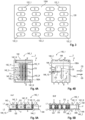
- Figure 3 is a partial plan view illustration a portion of an exemplary layout of source, drain and gate electrode metallizations at the first side 120A of the power transistor 120. The layout is shown from top, i.e. as it would be seen through the power transistor chip 120.
- a source electrode metallization 122_1 may include a plurality of source contact pads (S), and a drain electrode metallization 122_2 may include a plurality of drain contact pads (D). Further, a gate electrode metallization 122_3 is provided.
- the plurality of source contact pads (S) may, e.g., be arranged in a number of (horizontal) rows parallel to the longitudinal side of the power transistor chip 120.
- the plurality of drain contact pads (D) may be arranged in a number of (horizontal) rows parallel with the rows of the source contact pads (S).
- the rows of source contact pads (S) and the rows of drain contact pads (D) are interleaved (or alternating). Further, the source contact pads (S) and the drain contact pads D) are offset from each other in the longitudinal (horizontal) direction.
- the gate electrode metallization 122_3 may be arranged at a corner of the power transistor chip 120 and may, e.g., be formed by as single gate contact pad (G).
- the contact pad layout at the first side 120A of the power transistor chip 120 may, e.g., not include a source sense pad. That is, the multi-layer laminate substrate 140 (but, e.g., not an integrated circuitry of the power transistor chip 120) may provide the internal package interconnects between the source contact pads (S) of the power transistor chip 120 and the source package terminal pad 144_1 and the source sense package terminal pad 144_1S, respectively, of the transistor package 100.
- the (exemplary) layout of the source, drain and gate metallization 122_1, 122_2, 122_3 of the power transistor chip 120 apparently needs to be re-routed by a package-internal interconnect in order to provide for a layout of package terminal pads 144_1, 144_2, 144_3 and 144_1S as, e.g., shown in Figures 1A or 2A . Re-routing is carried out by the multi-layer laminate substrate 140.
- FIGS 4A-4B and 5A-5B illustrate a first example of a multi-layer laminate substrate 140, referred to as multi-layer laminate substrate 140_1 in the following.
- the multi-layer laminate substrate 140_1 includes a first structured metal layer 142, also referred to as L1 metal, and the second structured metal layer 144, also referred to as L2 metal.
- the first structured metal layer 142 faces the first side 120A of the power transistor chip 120.
- the first structured metal layer 142 may, e.g., include a multi-finger source segment 142_1, wherein fingers 142_1f of the multi-finger source segment 142_1 are connected to the source contact pads (S) of the source electrode metallization 122_1 of the power transistor chip 120.
- the first structured metal layer 142 may, e.g., include a multi-finger drain segment 142_2 having fingers 142_2f connected to the drain contact pads (D) of the drain electroe metallization 122_2 of the power transistor chip 120.
- the fingers 142_1f and the fingers 142_2f may, e.g., be interdigitated so as to allow to separately connect to the source contact pads (S) and the drain contact pads (S) at the first side 120A of the power transistor chip 120 (see, e.g., Figure 3 ).
- first structured metal layer 142 may include a gate segment 142_3 which connects to the gate contact pad 122_3 of the power transistor chip 120.
- the layout of the first structured metal layer 142 which is adapted to the layout of the source (S), drain (D) and gate (G) contact pads of the metallizations 122_1, 122_2, 122_3 of the power transistor chip 120, may be designed in a variety of different patterns.
- the layout of the first structured metal layer 142 is chosen to route the drain and source currents to different (e.g. opposite) sides of the transistor package 100.
- this separation of drain and source current is carried out by the fingers 142_1f, 142_2f of the multi-finger source and drain segments 142_1, 142_2, respectively.
- the fingers 142_1f or at least a part thereof may be connected to a rail portion 142_1r of the multi-finger source segment 142_1.
- the fingers 142_2f of the multi-finger drain segment 142_2 may be connected to a rail portion 142_2r of the multi-finger drain segment 142_2, wherein the rail portions 142_1r and 142_2r may be located at opposite sides of the transistor package 100.
- the rail portions 142_1r and 142r may, e.g., be parallel with each other and may, e.g., extend in X-direction.
- the fingers 142_1f, 142_2f may, e.g., be parallel with each other and may, e.g., extend in Y-direction, which is perpendicular to the X-direction.
- Figure 4B is a plan view of the second structured metal layer 144.
- the second structured metal layer 144 includes the source (S) package terminal pad 144_1, the drain (D) package terminal pad 144_2 and the gate (G) package terminal pad 144_3. Further, a source sense (SS) package terminal pad 144_1S is provided.
- S source
- D drain
- G gate
- SS source sense
- the source sense (SS) package terminal pad 144_1S and the source (S) package terminal pad 144_1 are formed by a continuous metal segment of the second structured metal layer 144.
- At least one insulating layer 540 is disposed between the first structured metal layer 142 (L1) and the second structured metal layer 144 (L2).
- a plurality of vias V is running through the insulating layer 540.
- the vias V connect segments of the first structured metal layer (L1) 142 to the terminal pads 144_1, 144_2, 144_3, 144_1S of the second structured metal layer 144 (L2). Vias V are indicated in Figures 4A-4B by circles.
- drain-source current path DS and the gate-source current path GS are indicated by arrows.
- the (large) drain-source current is flowing along the drain-source current path DS, while the (small) gate-source current is flowing along the gate-source current path GS.
- the drain-source current path DS between the source electrode metallization 122_1 of the power transistor chip 120 and the source (S) package terminal pad 144_1 flows on (at least) two structured layers of the multi-layer laminate substrate 140_1, namely on the first structured metal layer 142 (L1) and on the second structured metal layer 144 (L2).
- the gate-source current path GS between the source electrode metallization 122_1 of the power transistor chip 120 and the source sense (SS) package terminal pad 144_1S is provided only on one of the first and second structured metal layers 142 (L1), 144 (L2), namely on the second structured metal layer 144 (L2).
- the drain-source current path DS on the first and second structured metal layers 142, 144 is in the lateral Y-direction and the gate-source current path GS on the second structured metal layer 144 (L2) only is in the lateral X-direction, wherein the lateral Y-direction and the lateral X-direction are different from each other and, e.g., perpendicular to each other.
- the gate-source current only flows on one of those two layers (here: layer L2) in the X-direction, thereby partly decoupling the two current paths DS and GS.
- the gate segment 142_3 which connects the gate contact metallization 122_3 of the power transistor chip 120 through vias V to the gate (G) package terminal pad 144_3 of the transistor package 100 may be designed, e.g., to allow the gate (G) package terminal pad 144_3 to be located at a side of the transistor package 100 oriented in Y direction (this is also referred to as a "center gate layout").
- the source package terminal pad 144_1 may be arranged along a first side of the transistor package 100
- the drain package terminal pad 144_2 may be arranged along a second side opposite the first side of the transistor package 100
- the gate package terminal pad 144_3 may be arranged at a third side of the transistor package in a region spaced apart from a corner of the first or second side of the transistor package 100.
- FIGs 6A to 7B illustrate a second example of a multi-layer laminate substrate 140, referred to as multi-layer laminate substrate 140_2 in the following.
- the multi-layer laminate substrate 140_2 may be used in a transistor package in accordance with the first variant (see Figure 2A ).
- the source sense (SS) package terminal pad 144_1S and the source (S) package terminal pad 144_1 are formed by separate metal segments of the second structured metal layer 144 (L2).
- the drain-source current path DS is on the first and second structured metal layers 142 (L1) and 144 (L2), whereas the gate-source current path GS is only on the first structured metal layer 142 (L1).
- the drain-source current path DS on the first and second structured metal layers 142 (L1) and 144 (L2) is, e.g., in the lateral Y-direction.
- the gate-source current path GS on the first structured metal layer 142 is also, at least partially, in the Y-direction.
- gate-source current path GS may be (partially) in the X-direction along the rail 142_1r to a dedicated via dV through which the separate source sense (SS) package terminal pad 144_1S is connected to the first metal layer 142 (L1). No drain-source current is flowing through the dedicated via dV.
- the drain-source current flows on two metal layers L1, L2 of the multi-layer laminate substrate 140 in the Y-direction, while the gate-source current only flows on one (namely L1) of those two metal layers L1, L2 in (at least partially) the Y-direction and utilizes the dedicated via dV to connect to the insular source sense (SS) package terminal pad 144_1S at the package footprint.
- SS insular source sense
- the gate segment 142_3 which connects the gate contact metallization 122_3 of the power transistor chip 120 through vias V to the gate (G) package terminal pad 144_3 of the transistor package 100 may be, e.g., designed to allow the gate (G) package terminal pad 144_3 to be located at a corner of the transistor package 100 (this is also referred to as a "corner gate layout").
- the source package terminal pad 144_1 may be arranged along a first side of the transistor package 100
- the drain package terminal pad 144_2 may be arranged along a second side opposite the first side of the transistor package 100
- the gate package terminal pad 144_3 may be arranged at a corner of the first side of the transistor package 100.
- FIGS 8A to 9B illustrate a third example of a transistor package 100 which includes a third example of a multi-layer laminate substrate 143, referred to as multi-layer laminate substrate 140_3 in the following.
- the semiconductor package uses a dedicated via dV connecting to an insular source sense (SS) package terminal pad 144_1S.
- SS insular source sense
- S source
- FIG. 8A to 9B illustrate a third example of a transistor package 100 which includes a third example of a multi-layer laminate substrate 143, referred to as multi-layer laminate substrate 140_3 in the following.
- the semiconductor package uses a dedicated via dV connecting to an insular source sense (SS) package terminal pad 144_1S.
- the source sense (SS) package terminal pad 144_1S and the source (S) package terminal pad 144_1 are formed by separate metal segments of the second structured metal layer 144.
- the third example of a transistor package ( Figures 8A to 9B ) distinguishes from the second example ( Figures 6A to 7B ) in that the drain-source current path DS is only on the second structured metal layer 144 (L2) and the gate-source current path GS is only on the first structured metal layer 142 (L1).
- the multi-layer laminate substrate 140_3 provides fully decoupled drain-source and gate-source current paths DS and GS.
- the drain-source current path DS on the second structured metal layer 144 (L2) is in the Y-direction
- the gate-source current path GS on the first structured metal layer 142 (L1) is also, at least partially, in the Y-direction.
- the gate segment 142_3 which connects the gate contact metallization 122_3 of the power transistor chip 120 through vias V to the gate (G) package terminal pad 144_3 of the transistor package 100 may, e.g., designed to allow the gate (G) package terminal pad 144_3 to be located at a corner of the transistor package 100 ("corner gate layout").
- corner gate layout Reference is made to the above description of a "corner gate layout" to avoid reiteration.
- Table 1 ex. 1 (140_1) ex. 2 (140_2) ex. 3 (140_3) DS current through L1 + L2 L1 + L2 L2 GS current through L2 L1 L1 Dedicated via dV and insular SS pad No Yes Yes
- examples 1 and 2 multi-layer laminate substrates 140_1 and 140_2, respectively
- the example 3 fully decouples the drain-source current path DS and the gate-source current pat GS.
- the source sense (SS) terminal pad 144_1S ("Kelvin source pad") for the gate-source current is connected to the power transistor chip 120 on only one of the metal layers L1, L2, and the at least one other metal layer L2 or L1, respectively, is used to provide an alternate path for the drain-source current between the source electrode metallization 122_1 of the power transistor chip 120 and the (power) source package terminal pad 144_1 of the transistor package 100.
- a dedicated via dV can be used either in a partially decoupled implementation (e.g. ex. 2, 140_2) or a fully decoupled implementation (e.g. ex. 3, 140_3).
- center gate or corner gate layouts may be used in any of the implementations as disclosed.
- Figure 10 is a perspective top view of detail DT of Figure 1 .
- the semi-transparent representation shows the dedicated via dV connecting to the insular source sense (SS) package terminal pad 144_1S (SS).
- SS insular source sense
- FIGS 2A and Figures 6A to 9B in which implementations in line with such footprint layout are presented, for example.
- the transistor packages 100 disclosed herein allow to achieve low parasitics for fast switching and high thermal connectivity.
- the array of vias V provides a vertical connection structure of low parasitic inductance in the multi-layer laminate structure 140 to connect the source electrode metallization 122_1 of the power transistor chip 120 to the source package terminal pad 144_1 of the transistor package 100.
- the partially or fully decoupling of the (large) load DS and the (small) source sense GS currents allows to offer a source Kelvin IO pin (i.e. the source sense package terminal pad 144_1S) with minimum parasitic inductance.
- a dedicated via dV connecting the source electrode metallization 122_1 of the power transistor chip 120 to the source sense (SS) package terminal pad 144_1S of the transistor package 100 may improve the switching frequency.
- the face-down orientation of the GaN transistor chip 120 in combination with the multi-layer laminate substrate 140, which can be used as a routable base of the transistor package 100 allows to align the transistor package footprint with the footprints of common MOSFET (Metal Oxide Semiconductor Field Effect Transistor) packages which, however, cannot fulfill the fast switching requirements of the transistor package 100 described herein.
- MOSFET Metal Oxide Semiconductor Field Effect Transistor
- the multi-layer laminate substrate 140 may be represented by a variety of different structures and formed by a variety of different methods of manufacturing.
- the multi-layer laminate substrate 140 may comprise or be a separate PCB (Printed Circuit Board) on which the power transistor chip 120 chip is mounted.
- the multi-layer laminate substrate may be generated at wafer level by, e.g., embedded wafer level packaging techniques, also known as eWLP in the art.
- eWLP embedded wafer level packaging techniques
- the transistor packages 100 are separated from an "artificial wafer" in which an array of power transistor chips 120 is embedded in a continuous mold compound wafer structure.
Landscapes
- Junction Field-Effect Transistors (AREA)
Abstract
Description
- This disclosure relates generally to the technique of semiconductor packaging, and in particular to a transistor package for a lateral transistor device.
- Transistor packages are widely used as electronic switches in a variety of electronic circuits. Higher efficiency, increased power density, lower switching losses, faster switching times, lower device parasitics and lower cost are among the key goals for next generation transistor package design.
- The transistor switching performance is limited by parasitic elements from the transistor package and the board. In particular, the parasitic common source inductance causes switching losses.
- Conventional approaches to reduce device parasitics for fast switching and to improve thermal behavior are to use leadless packages and/or to use clips for connecting the load electrodes of a semiconductor transistor chip to the respective terminals of the transistor package.
- Existing package solutions use an additional pin for a source Kelvin connection as a reference potential for the gate driving voltage. However, the presence of a source Kelvin pin and source Kelvin connection degrades the package inductance and package resistance.
- According to an aspect of the disclosure, a transistor package for a power transistor chip includes the power transistor chip having a first side and a second side opposite the first side. The first side comprises a source electrode metallization, a drain electrode metallization and a gate electrode metallization. The package further includes a multi-layer laminate substrate to which the power transistor chip is connected. The multi-layer laminate substrate comprises a first structured metal layer facing the first side of the power transistor chip and being electrically connected to the source electrode metallization, the drain electrode metallization and the gate electrode metallization, a second structured metal layer comprising a source package terminal pad, a source sense package terminal pad, a drain package terminal pad and a gate package terminal pad, at least one insulating layer disposed between the first structured metal layer and the second structured metal layer, and a plurality of vias running through the insulating layer and connecting segments of the first structured metal layer to the terminal pads of the second structured metal layer. The first structured metal layer, the second structured metal layer and the plurality of vias are designed such that a gate-source current path between the power transistor chip and the source sense package terminal pad is provided only on one of the first and second structured metal layers while a drain-source current path between the source electrode metallization of the power transistor chip and the source package terminal pad is at least on the other structured metal layer of the multi-layer laminate substrate.
- In the drawings, like reference numerals designate corresponding similar parts. The features of the various illustrated embodiments can be combined unless they exclude each other and/or can be selectively omitted if not described to be necessarily required. Embodiments are depicted in the drawings and are exemplarily detailed in the description which follows.
-
Figure 1 is a perspective top view of an example of a transistor package illustrated in a semi-transparent representation. -
Figure 2A is a bottom view a transistor package in accordance with a first variant. -
Figure 2B is a bottom view of a transistor package in accordance with a second variant. -
Figure 3 is a plan view of a portion of an exemplary electrode metallization layout of a power transistor chip. -
Figure 4A is a plan view of a first structured metal layer facing the power transistor chip according to a first example of a transistor package. -
Figure 4B is a plan view of a second structured metal layer the transistor package ofFigure 4A . -
Figure 5A is a schematic cross-sectional view of the transistor package ofFigures 4A, 4B along line A-A' ofFigures 4A and 4B . -
Figure 5B is a schematic cross-sectional view of the transistor package ofFigures 4A, 4B along line B-B' ofFigures 4A and 4B . -
Figure 6A is a plan view of a first structured metal layer facing the power transistor chip according to a second example of a transistor package. -
Figure 6B is a plan view of a second structured metal layer the transistor package ofFigure 6A . -
Figure 7A is a schematic cross-sectional view of the transistor package ofFigures 6A, 6B along line A-A' ofFigures 6A and 6B . -
Figure 7B is a schematic cross-sectional view of the transistor package ofFigures 6A, 6B along line B-B' ofFigures 6A and 6B . -
Figure 8A is a plan view of a first structured metal layer facing the power transistor chip according to a third example of a transistor package. -
Figure 8B is a plan view of a second structured metal layer the transistor package ofFigure 8A . -
Figure 9A is a schematic cross-sectional view of the transistor package ofFigures 8A, 8B along line A-A' ofFigures 8A and 8B . -
Figure 9B is a schematic cross-sectional view of the transistor package ofFigures 8A, 8B along line B-B' ofFigures 8A and 8B . -
Figure 10 is a perspective top view of a detail ofFigure 1 . - As used in this specification, the terms "electrically connected" or "electrically coupled" or similar terms are not meant to mean that the elements are directly contacted together; intervening elements may be provided between the "electrically connected" or "electrically coupled" elements, respectively. However, in accordance with the disclosure, the above-mentioned and similar terms may, optionally, also have the specific meaning that the elements are directly contacted together, i.e. that no intervening elements are provided between the "electrically connected" or "electrically coupled" elements, respectively.
- Further, the words "over" or "beneath" with regard to a part, element or material layer formed or located or arranged "over" or "beneath" a surface may be used herein to mean that the part, element or material layer be located (e.g. placed, formed, arranged, deposited, etc.) "directly on" or "directly under", e.g. in direct contact with, the implied surface. The word "over" or "beneath" used with regard to a part, element or material layer formed or located or arranged "over" or "beneath" a surface may, however, either be used herein to mean that the part, element or material layer be located (e.g. placed, formed, arranged, deposited, etc.) "indirectly on" or "indirectly under" the implied surface, with one or more additional parts, elements or layers being arranged between the implied surface and the part, element or material layer.
- Referring to
Figure 1 , atransistor package 100 includes apower transistor chip 120. Thepower transistor chip 120 has a first side (not visible inFigure 1 ) and asecond side 120B opposite the first side. - The
semiconductor transistor chip 120 is a lateral device, i.e. the first side comprises a source electrode metallization, a drain electrode metallization and a gate electrode metallization. The metallizations are all disposed on the same (first) side of thesemiconductor transistor chip 120. In other words, the lateralsemiconductor transistor chip 120 is implemented in thetransistor package 100 in a flip-chip orientation. - The
power transistor chip 120 may be, e.g., capable of switching high currents and/or medium or high voltages (e.g. more than 50 V or 100 V or 200 V or 300 V blocking voltage). In particular, exemplary transistor packages as disclosed herein may operate in the medium voltage (MV) range, in which the blocking voltage is equal to or greater than or less than 200 V or 150 V or 100 V or 50 V. - The
power transistor chip 120 may be of different types. Examples described herein are, in particular, directed, e.g., to HEMT (high electron mobility transistor) devices. More specifically, thesemiconductor transistor chip 120 referred to herein may, e.g., be a III-V compound semiconductor chip having, e.g., a high band gap. Thepower transistor chip 120 may, e.g., be a GaN chip. In this case, the GaNchip 120 may be a lateral GaN-on-substrate device such as a GaN-on-Si device or a GaN-on-SiC device or a GaN-on-sapphire device, for example. - The
transistor package 100 may include a multi-layer laminate substrate (will be described further below) to which thepower transistor chip 120 is connected (e.g. mounted). - The source, drain and gate electrode metallizations of the
power transistor chip 120 are connected via a first structured metal layer (will be described further below) of the multi-layer laminate substrate to a second structuredmetal layer 144 of multi-layer laminate substrate. The second structuredmetal layer 144 may be exposed at the bottom of thetransistor package 100 and includes a source package terminal pad 144_1 also denoted by S, a drain package terminal pad 144_2 also denoted by D, and a gate package terminal pad 144_3 also denoted by G, see, e.g., the exemplary footprints oftransistor packages 100 shown inFigures 2A and 2B . - As illustrated in the semi-transparent representation of
Figure 1 , thepower transistor chip 120 may be embedded in amold compound 180. Themold compound 180 may cover the multi-layer laminate substrate to which thepower transistor chip 120 is connected. A periphery of themold compound 180 is denoted byreference sign 180A. - The second structured
metal layer 144, providing for the package terminals, further includes a source sense package terminal pad 144_1S also denoted by SS. The source sense package terminal pad 144_1S, which is also referred to as Kelvin sense terminal pad in the art, may, e.g., be implemented either as an separate (insular) package terminal pad (Figure 2A ) or as a terminal pad which is continuous with the source package terminal 144_1 (Figure 2B ). As will be described in the following, both variants (Figure 2A : separate source sense package terminal pad 144_1S; orFigure 2B : integral source sense package terminal pad 144_1S) can be designed to provide low device parasitics and therefore fast switching oftransistor packages 100 described herein. -
Figure 3 is a partial plan view illustration a portion of an exemplary layout of source, drain and gate electrode metallizations at thefirst side 120A of thepower transistor 120. The layout is shown from top, i.e. as it would be seen through thepower transistor chip 120. - A source electrode metallization 122_1 may include a plurality of source contact pads (S), and a drain electrode metallization 122_2 may include a plurality of drain contact pads (D). Further, a gate electrode metallization 122_3 is provided.
- The plurality of source contact pads (S) may, e.g., be arranged in a number of (horizontal) rows parallel to the longitudinal side of the
power transistor chip 120. Likewise, the plurality of drain contact pads (D) may be arranged in a number of (horizontal) rows parallel with the rows of the source contact pads (S). In the example shown inFigure 3 , the rows of source contact pads (S) and the rows of drain contact pads (D) are interleaved (or alternating). Further, the source contact pads (S) and the drain contact pads D) are offset from each other in the longitudinal (horizontal) direction. The gate electrode metallization 122_3 may be arranged at a corner of thepower transistor chip 120 and may, e.g., be formed by as single gate contact pad (G). - The contact pad layout at the
first side 120A of thepower transistor chip 120 may, e.g., not include a source sense pad. That is, the multi-layer laminate substrate 140 (but, e.g., not an integrated circuitry of the power transistor chip 120) may provide the internal package interconnects between the source contact pads (S) of thepower transistor chip 120 and the source package terminal pad 144_1 and the source sense package terminal pad 144_1S, respectively, of thetransistor package 100. - The (exemplary) layout of the source, drain and gate metallization 122_1, 122_2, 122_3 of the
power transistor chip 120 apparently needs to be re-routed by a package-internal interconnect in order to provide for a layout of package terminal pads 144_1, 144_2, 144_3 and 144_1S as, e.g., shown inFigures 1A or 2A . Re-routing is carried out by themulti-layer laminate substrate 140. -
Figures 4A-4B and 5A-5B illustrate a first example of amulti-layer laminate substrate 140, referred to as multi-layer laminate substrate 140_1 in the following. The multi-layer laminate substrate 140_1 includes a firststructured metal layer 142, also referred to as L1 metal, and the secondstructured metal layer 144, also referred to as L2 metal. - The first
structured metal layer 142 faces thefirst side 120A of thepower transistor chip 120. The firststructured metal layer 142 may, e.g., include a multi-finger source segment 142_1, wherein fingers 142_1f of the multi-finger source segment 142_1 are connected to the source contact pads (S) of the source electrode metallization 122_1 of thepower transistor chip 120. Further, the firststructured metal layer 142 may, e.g., include a multi-finger drain segment 142_2 having fingers 142_2f connected to the drain contact pads (D) of the drain electroe metallization 122_2 of thepower transistor chip 120. The fingers 142_1f and the fingers 142_2f may, e.g., be interdigitated so as to allow to separately connect to the source contact pads (S) and the drain contact pads (S) at thefirst side 120A of the power transistor chip 120 (see, e.g.,Figure 3 ). - Further, the first
structured metal layer 142 may include a gate segment 142_3 which connects to the gate contact pad 122_3 of thepower transistor chip 120. - It is to be noted that a variety of different layouts of the source (S), drain (D) and gate (G) contact pads of the metallizations 122_1, 122_2, 122_3 at the
first side 120A of thepower transistor chip 120 is possible. Correspondingly, the layout of the firststructured metal layer 142, which is adapted to the layout of the source (S), drain (D) and gate (G) contact pads of the metallizations 122_1, 122_2, 122_3 of thepower transistor chip 120, may be designed in a variety of different patterns. - In many examples the layout of the first
structured metal layer 142 is chosen to route the drain and source currents to different (e.g. opposite) sides of thetransistor package 100. In the specific example shown inFigures 4A-5B , this separation of drain and source current is carried out by the fingers 142_1f, 142_2f of the multi-finger source and drain segments 142_1, 142_2, respectively. To this end, the fingers 142_1f or at least a part thereof (as in the example shown) may be connected to a rail portion 142_1r of the multi-finger source segment 142_1. Likewise, the fingers 142_2f of the multi-finger drain segment 142_2 may be connected to a rail portion 142_2r of the multi-finger drain segment 142_2, wherein the rail portions 142_1r and 142_2r may be located at opposite sides of thetransistor package 100. - The rail portions 142_1r and 142r may, e.g., be parallel with each other and may, e.g., extend in X-direction. The fingers 142_1f, 142_2f may, e.g., be parallel with each other and may, e.g., extend in Y-direction, which is perpendicular to the X-direction.
-
Figure 4B is a plan view of the secondstructured metal layer 144. The secondstructured metal layer 144 includes the source (S) package terminal pad 144_1, the drain (D) package terminal pad 144_2 and the gate (G) package terminal pad 144_3. Further, a source sense (SS) package terminal pad 144_1S is provided. - In a first example, the source sense (SS) package terminal pad 144_1S and the source (S) package terminal pad 144_1 are formed by a continuous metal segment of the second
structured metal layer 144. - At least one insulating
layer 540 is disposed between the first structured metal layer 142 (L1) and the second structured metal layer 144 (L2). A plurality of vias V is running through the insulatinglayer 540. The vias V connect segments of the first structured metal layer (L1) 142 to the terminal pads 144_1, 144_2, 144_3, 144_1S of the second structured metal layer 144 (L2). Vias V are indicated inFigures 4A-4B by circles. - In
Figures 4A to 5B the drain-source current path DS and the gate-source current path GS are indicated by arrows. The (large) drain-source current is flowing along the drain-source current path DS, while the (small) gate-source current is flowing along the gate-source current path GS. - As apparent from
Figures 4A to 5B , the drain-source current path DS between the source electrode metallization 122_1 of thepower transistor chip 120 and the source (S) package terminal pad 144_1 flows on (at least) two structured layers of the multi-layer laminate substrate 140_1, namely on the first structured metal layer 142 (L1) and on the second structured metal layer 144 (L2). On the other hand, the gate-source current path GS between the source electrode metallization 122_1 of thepower transistor chip 120 and the source sense (SS) package terminal pad 144_1S is provided only on one of the first and second structured metal layers 142 (L1), 144 (L2), namely on the second structured metal layer 144 (L2). - For example, the drain-source current path DS on the first and second
structured metal layers - In other words, while the drain-source current flows on two layers L1, L2 of the
transistor package 100 in the Y-direction, the gate-source current only flows on one of those two layers (here: layer L2) in the X-direction, thereby partly decoupling the two current paths DS and GS. - Further, the gate segment 142_3 which connects the gate contact metallization 122_3 of the
power transistor chip 120 through vias V to the gate (G) package terminal pad 144_3 of thetransistor package 100 may be designed, e.g., to allow the gate (G) package terminal pad 144_3 to be located at a side of thetransistor package 100 oriented in Y direction (this is also referred to as a "center gate layout"). That is, the source package terminal pad 144_1 may be arranged along a first side of thetransistor package 100, the drain package terminal pad 144_2 may be arranged along a second side opposite the first side of thetransistor package 100 and the gate package terminal pad 144_3 may be arranged at a third side of the transistor package in a region spaced apart from a corner of the first or second side of thetransistor package 100. -
Figures 6A to 7B illustrate a second example of amulti-layer laminate substrate 140, referred to as multi-layer laminate substrate 140_2 in the following. The multi-layer laminate substrate 140_2 may be used in a transistor package in accordance with the first variant (seeFigure 2A ). In other words, the source sense (SS) package terminal pad 144_1S and the source (S) package terminal pad 144_1 are formed by separate metal segments of the second structured metal layer 144 (L2). - As illustrated in
Figures 6A to 7B , the drain-source current path DS is on the first and second structured metal layers 142 (L1) and 144 (L2), whereas the gate-source current path GS is only on the first structured metal layer 142 (L1). The drain-source current path DS on the first and second structured metal layers 142 (L1) and 144 (L2) is, e.g., in the lateral Y-direction. The gate-source current path GS on the firststructured metal layer 142 is also, at least partially, in the Y-direction. Further, gate-source current path GS may be (partially) in the X-direction along the rail 142_1r to a dedicated via dV through which the separate source sense (SS) package terminal pad 144_1S is connected to the first metal layer 142 (L1). No drain-source current is flowing through the dedicated via dV. - In other words, in the second example of a
transistor package 100 the drain-source current flows on two metal layers L1, L2 of themulti-layer laminate substrate 140 in the Y-direction, while the gate-source current only flows on one (namely L1) of those two metal layers L1, L2 in (at least partially) the Y-direction and utilizes the dedicated via dV to connect to the insular source sense (SS) package terminal pad 144_1S at the package footprint. - Further, the gate segment 142_3 which connects the gate contact metallization 122_3 of the
power transistor chip 120 through vias V to the gate (G) package terminal pad 144_3 of thetransistor package 100 may be, e.g., designed to allow the gate (G) package terminal pad 144_3 to be located at a corner of the transistor package 100 (this is also referred to as a "corner gate layout"). For example, the source package terminal pad 144_1 may be arranged along a first side of thetransistor package 100, the drain package terminal pad 144_2 may be arranged along a second side opposite the first side of thetransistor package 100 and the gate package terminal pad 144_3 may be arranged at a corner of the first side of thetransistor package 100. -
Figures 8A to 9B illustrate a third example of atransistor package 100 which includes a third example of a multi-layer laminate substrate 143, referred to as multi-layer laminate substrate 140_3 in the following. Similar to the multi-layer laminate substrate 140_2, the semiconductor package uses a dedicated via dV connecting to an insular source sense (SS) package terminal pad 144_1S. Differently stated, the source sense (SS) package terminal pad 144_1S and the source (S) package terminal pad 144_1 are formed by separate metal segments of the secondstructured metal layer 144. However, the third example of a transistor package (Figures 8A to 9B ) distinguishes from the second example (Figures 6A to 7B ) in that the drain-source current path DS is only on the second structured metal layer 144 (L2) and the gate-source current path GS is only on the first structured metal layer 142 (L1). The multi-layer laminate substrate 140_3 provides fully decoupled drain-source and gate-source current paths DS and GS. - For example, the drain-source current path DS on the second structured metal layer 144 (L2) is in the Y-direction, and the gate-source current path GS on the first structured metal layer 142 (L1) is also, at least partially, in the Y-direction.
- Further, the gate segment 142_3 which connects the gate contact metallization 122_3 of the
power transistor chip 120 through vias V to the gate (G) package terminal pad 144_3 of thetransistor package 100 may, e.g., designed to allow the gate (G) package terminal pad 144_3 to be located at a corner of the transistor package 100 ("corner gate layout"). Reference is made to the above description of a "corner gate layout" to avoid reiteration. - The various implementations according the first, second and third examples disclosed above are summarized in Table 1.
Table 1 ex. 1 (140_1) ex. 2 (140_2) ex. 3 (140_3) DS current through L1 + L2 L1 + L2 L2 GS current through L2 L1 L1 Dedicated via dV and insular SS pad No Yes Yes - While examples 1 and 2 (multi-layer laminate substrates 140_1 and 140_2, respectively) provide for partial decoupling of the drain-source current and the gate-source current, the example 3 fully decouples the drain-source current path DS and the gate-source current pat GS. In all examples 1 to 3 the source sense (SS) terminal pad 144_1S ("Kelvin source pad") for the gate-source current is connected to the
power transistor chip 120 on only one of the metal layers L1, L2, and the at least one other metal layer L2 or L1, respectively, is used to provide an alternate path for the drain-source current between the source electrode metallization 122_1 of thepower transistor chip 120 and the (power) source package terminal pad 144_1 of thetransistor package 100. Further, it is to be noted that a dedicated via dV can be used either in a partially decoupled implementation (e.g. ex. 2, 140_2) or a fully decoupled implementation (e.g. ex. 3, 140_3). Moreover, center gate or corner gate layouts may be used in any of the implementations as disclosed. -
Figure 10 is a perspective top view of detail DT ofFigure 1 . The semi-transparent representation shows the dedicated via dV connecting to the insular source sense (SS) package terminal pad 144_1S (SS). Reference is made toFigures 2A andFigures 6A to 9B in which implementations in line with such footprint layout are presented, for example. - Due to the face-down orientation of the
semiconductor transistor chip 120, the transistor packages 100 disclosed herein allow to achieve low parasitics for fast switching and high thermal connectivity. In all examples, the array of vias V provides a vertical connection structure of low parasitic inductance in themulti-layer laminate structure 140 to connect the source electrode metallization 122_1 of thepower transistor chip 120 to the source package terminal pad 144_1 of thetransistor package 100. In addition, the partially or fully decoupling of the (large) load DS and the (small) source sense GS currents allows to offer a source Kelvin IO pin (i.e. the source sense package terminal pad 144_1S) with minimum parasitic inductance. In particular, a dedicated via dV connecting the source electrode metallization 122_1 of thepower transistor chip 120 to the source sense (SS) package terminal pad 144_1S of thetransistor package 100 may improve the switching frequency. - Further, for example given a GaN
semiconductor transistor chip 120 is used, the face-down orientation of theGaN transistor chip 120 in combination with themulti-layer laminate substrate 140, which can be used as a routable base of thetransistor package 100, allows to align the transistor package footprint with the footprints of common MOSFET (Metal Oxide Semiconductor Field Effect Transistor) packages which, however, cannot fulfill the fast switching requirements of thetransistor package 100 described herein. - The
multi-layer laminate substrate 140 may be represented by a variety of different structures and formed by a variety of different methods of manufacturing. For example, themulti-layer laminate substrate 140 may comprise or be a separate PCB (Printed Circuit Board) on which thepower transistor chip 120 chip is mounted. In other examples, the multi-layer laminate substrate may be generated at wafer level by, e.g., embedded wafer level packaging techniques, also known as eWLP in the art. In eWLP, the transistor packages 100 are separated from an "artificial wafer" in which an array of power transistor chips 120 is embedded in a continuous mold compound wafer structure. - The following examples pertain to further aspects of the disclosure:
- Example 1 is a transistor package for a power transistor chip. The transistor package includes the power transistor chip having a first side and a second side opposite the first side. The first side comprises a source electrode metallization, a drain electrode metallization and a gate electrode metallization. The package further includes a multi-layer laminate substrate to which the power transistor chip is connected. The multi-layer laminate substrate comprises a first structured metal layer facing the first side of the power transistor chip and being electrically connected to the source electrode metallization, the drain electrode metallization and the gate electrode metallization, a second structured metal layer comprising a source package terminal pad, a source sense package terminal pad, a drain package terminal pad and a gate package terminal pad, at least one insulating layer disposed between the first structured metal layer and the second structured metal layer, and a plurality of vias running through the insulating layer and connecting segments of the first structured metal layer to the terminal pads of the second structured metal layer. The first structured metal layer, the second structured metal layer and the plurality of vias are designed such that a gate-source current path between the power transistor chip and the source sense package terminal pad is provided only on one of the first and second structured metal layers while a drain-source current path between the source electrode metallization of the power transistor chip and the source package terminal pad is at least on the other structured metal layer of the multi-layer laminate substrate.
- In Example 2, the subject matter of Example 1 can optionally include wherein the source sense package terminal pad and the source package terminal pad are formed by a continuous metal segment of the second structured metal layer.
- In Example 3, the subject matter of Example 1 or 2 can optionally include wherein the drain-source current path is on the first and second structured metal layers, and the gate-source current path is only on the second structured metal layer.
- In Example 4, the subject matter of Example 3 can optionally include wherein the drain-source current path on the first and second structured metal layers is in a lateral direction Y and the gate-source current path on the second structured metal layer is in a lateral direction X, wherein the lateral direction Y and the lateral direction X are different from each other.
- In Example 5, the subject matter of Example 1 can optionally include wherein the source sense package terminal pad and the source package terminal pad are formed by separate metal segments of the second structured metal layer.
- In Example 6, the subject matter of Example 5 can optionally include wherein the drain-source current path is on the first and second structured metal layers, and the gate-source current path is only on the first structured metal layer.
- In Example 7, the subject matter of Example 6 can optionally include wherein the drain-source current path on the first and second structured metal layers is in a lateral direction Y and the gate-source current path on the first structured metal layer is also at least partially in the lateral direction Y.
- In Example 8, the subject matter of Example 5 can optionally include wherein the drain-source current path is only on the second structured metal layer, and the gate-source current path is only on the first structured metal layer.
- In Example 9, the subject matter of Example 8 can optionally include wherein the drain-source current path on the second structured metal layer is in a lateral direction Y and the gate-source current path on the first structured metal layer is also at least partially in the lateral direction Y.
- In Example 10, the subject matter of any of Examples 5 to 9 can optionally include wherein the separate source sense package terminal pad is connected to the first metal layer by a dedicated via through which no drain-source current is flowing.
- In Example 11, the subject matter of any of the preceding Examples can optionally include wherein the first structured metal layer comprises a multi-finger drain segment connected to the drain electrode metallization and a multi-finger source segment connected to the source electrode metallization, wherein the multi-finger drain segment and the multi-finger source segment are interdigitated.
- In Example 12, the subject matter of any of the preceding Examples can optionally include wherein the source package terminal pad is arranged along a first side of the transistor package, the drain package terminal pad is arranged along a second side opposite the first side of the transistor package and the gate package terminal pad is arranged at a corner of the first side of the transistor package.
- In Example 13, the subject matter of any of the Examples 1 to 11 can optionally include wherein the source package terminal pad is arranged along a first side of the transistor package, the drain package terminal pad is arranged along a second side opposite the first side of the transistor package and the gate package terminal pad is arranged at a third side of the transistor package in a region spaced apart from a corner of the first or second side of the transistor package.
- In Example 14, the subject matter of any of the preceding Examples can optionally further include a mold compound embedding the power transistor chip and covering the multi-layer laminate substrate outside the area where the power transistor chip is placed.
- In Example 15, the subject matter of any of the preceding Examples can optionally include wherein the power transistor chip is a HEMT transistor chip and/or a GaN transistor chip.
- In Example 16, the subject matter of any of the preceding Examples can optionally include wherein the power transistor chip is configured to switch drain-source voltages equal to or greater than 50 V or 100 V or 150 V or 200 V.
- Although specific embodiments have been illustrated and described herein, it will be appreciated by those of ordinary skill in the art that a variety of alternate and/or equivalent implementations may be substituted for the specific embodiments shown and described without departing from the scope of the present invention. This application is intended to cover any adaptations or variations of the specific embodiments discussed herein. Therefore, it is intended that this invention be limited only by the claims and the equivalents thereof.
Claims (16)
- A transistor package for a power transistor chip, the transistor package comprising:the power transistor chip having a first side and a second side opposite the first side, the first side comprising a source electrode metallization, a drain electrode metallization and a gate electrode metallization; anda multi-layer laminate substrate to which the power transistor chip is connected, the multi-layer laminate substrate comprisinga first structured metal layer facing the first side of the power transistor chip and being electrically connected to the source electrode metallization, the drain electrode metallization and the gate electrode metallization;a second structured metal layer comprising a source package terminal pad, a source sense package terminal pad, a drain package terminal pad and a gate package terminal pad;at least one insulating layer disposed between the first structured metal layer and the second structured metal layer; anda plurality of vias running through the insulating layer and connecting segments of the first structured metal layer to the terminal pads of the second structured metal layer; whereinthe first structured metal layer, the second structured metal layer and the plurality of vias are designed such that a gate-source current path between the power transistor chip and the source sense package terminal pad is provided only on one of the first and second structured metal layers while a drain-source current path between the source electrode metallization of the power transistor chip and the source package terminal pad is at least on the other structured metal layer of the multi-layer laminate substrate.
- The transistor package of claim 1, wherein the source sense package terminal pad and the source package terminal pad are formed by a continuous metal segment of the second structured metal layer.
- The transistor package of claim 1 or 2, wherein the drain-source current path is on the first and second structured metal layers, and the gate-source current path is only on the second structured metal layer.
- The transistor package of claim 3, wherein the drain-source current path on the first and second structured metal layers is in a lateral direction Y and the gate-source current path on the second structured metal layer is in a lateral direction X, wherein the lateral direction Y and the lateral direction X are different from each other.
- The transistor package of claim 1, wherein the source sense package terminal pad and the source package terminal pad are formed by separate metal segments of the second structured metal layer.
- The transistor package of claim 5, wherein the drain-source current path is on the first and second structured metal layers, and the gate-source current path is only on the first structured metal layer.
- The transistor package of claim 6, wherein the drain-source current path on the first and second structured metal layers is in a lateral direction Y and the gate-source current path on the first structured metal layer is also at least partially in the lateral direction Y.
- The transistor package of claim 5, wherein the drain-source current path is only on the second structured metal layer, and the gate-source current path is only on the first structured metal layer.
- The transistor package of claim 8, wherein the drain-source current path on the second structured metal layer is in a lateral direction Y and the gate-source current path on the first structured metal layer is also at least partially in the lateral direction Y.
- The transistor package of any one of claims 5 to 9, wherein the separate source sense package terminal pad is connected to the first metal layer by a dedicated via through which no drain-source current is flowing.
- The transistor package of any preceding claim, wherein the first structured metal layer comprises a multi-finger drain segment connected to the drain electrode metallization and a multi-finger source segment connected to the source electrode metallization, wherein the multi-finger drain segment and the multi-finger source segment are interdigitated.
- The transistor package of any preceding claim, wherein the source package terminal pad is arranged along a first side of the transistor package, the drain package terminal pad is arranged along a second side opposite the first side of the transistor package and the gate package terminal pad is arranged at a corner of the first side of the transistor package.
- The transistor package of any of claims 1 to 11, wherein the source package terminal pad is arranged along a first side of the transistor package, the drain package terminal pad is arranged along a second side opposite the first side of the transistor package and the gate package terminal pad is arranged at a third side of the transistor package in a region spaced apart from a corner of the first or second side of the transistor package.
- The transistor package of any preceding claim, further comprising:
a mold compound embedding the power transistor chip and covering the multi-layer laminate substrate outside the area where the power transistor chip is placed. - The transistor package of any preceding claim, wherein the power transistor chip is a HEMT transistor chip and/or a GaN transistor chip.
- The transistor package of any preceding claim, wherein the power transistor chip is configured to switch drain-source voltages equal to or greater than 50 V or 100 V or 150 V or 200 V.
Priority Applications (3)
| Application Number | Priority Date | Filing Date | Title |
|---|---|---|---|
| EP22206772.0A EP4369395B1 (en) | 2022-11-10 | 2022-11-10 | Package for a lateral power transistor |
| US18/488,084 US20240162136A1 (en) | 2022-11-10 | 2023-10-17 | Package for a lateral power transistor |
| CN202311498861.2A CN118016628A (en) | 2022-11-10 | 2023-11-10 | Package for lateral power transistors |
Applications Claiming Priority (1)
| Application Number | Priority Date | Filing Date | Title |
|---|---|---|---|
| EP22206772.0A EP4369395B1 (en) | 2022-11-10 | 2022-11-10 | Package for a lateral power transistor |
Publications (2)
| Publication Number | Publication Date |
|---|---|
| EP4369395A1 true EP4369395A1 (en) | 2024-05-15 |
| EP4369395B1 EP4369395B1 (en) | 2025-08-27 |
Family
ID=84361764
Family Applications (1)
| Application Number | Title | Priority Date | Filing Date |
|---|---|---|---|
| EP22206772.0A Active EP4369395B1 (en) | 2022-11-10 | 2022-11-10 | Package for a lateral power transistor |
Country Status (3)
| Country | Link |
|---|---|
| US (1) | US20240162136A1 (en) |
| EP (1) | EP4369395B1 (en) |
| CN (1) | CN118016628A (en) |
Families Citing this family (2)
| Publication number | Priority date | Publication date | Assignee | Title |
|---|---|---|---|---|
| US12599008B2 (en) * | 2023-04-06 | 2026-04-07 | Nxp Usa, Inc. | Transistor with source manifold in non-active die region |
| CN121192081A (en) * | 2024-06-21 | 2025-12-23 | 华为技术有限公司 | An electrical connection substrate, a chip packaging structure, and an electronic device. |
Citations (1)
| Publication number | Priority date | Publication date | Assignee | Title |
|---|---|---|---|---|
| US20020076851A1 (en) * | 2000-07-13 | 2002-06-20 | Eden Richard C. | Power semiconductor switching devices, power converters, integrated circuit assemblies, integrated circuitry, power current switching methods, methods of forming a power semiconductor switching device, power conversion methods, power semiconductor switching device packaging methods, and methods of forming a power transistor |
-
2022
- 2022-11-10 EP EP22206772.0A patent/EP4369395B1/en active Active
-
2023
- 2023-10-17 US US18/488,084 patent/US20240162136A1/en active Pending
- 2023-11-10 CN CN202311498861.2A patent/CN118016628A/en active Pending
Patent Citations (1)
| Publication number | Priority date | Publication date | Assignee | Title |
|---|---|---|---|---|
| US20020076851A1 (en) * | 2000-07-13 | 2002-06-20 | Eden Richard C. | Power semiconductor switching devices, power converters, integrated circuit assemblies, integrated circuitry, power current switching methods, methods of forming a power semiconductor switching device, power conversion methods, power semiconductor switching device packaging methods, and methods of forming a power transistor |
Also Published As
| Publication number | Publication date |
|---|---|
| CN118016628A (en) | 2024-05-10 |
| US20240162136A1 (en) | 2024-05-16 |
| EP4369395B1 (en) | 2025-08-27 |
Similar Documents
| Publication | Publication Date | Title |
|---|---|---|
| US7166898B2 (en) | Flip chip FET device | |
| US9589869B2 (en) | Packaging solutions for devices and systems comprising lateral GaN power transistors | |
| US20240162136A1 (en) | Package for a lateral power transistor | |
| JP6973406B2 (en) | Semiconductor module | |
| US20130105960A1 (en) | Low Stray Inductance Power Module | |
| US12040257B2 (en) | Device topology for lateral power transistors with low common source inductance | |
| US20080099926A1 (en) | Semiconductor device | |
| US11107739B2 (en) | Power semiconductor module arrangement | |
| JP3708082B2 (en) | Power semiconductor device | |
| US12628699B2 (en) | Packaged electronic device comprising a plurality of power transistors | |
| US7821128B2 (en) | Power semiconductor device having lines within a housing | |
| US11973071B2 (en) | Semiconductor module | |
| US12482730B2 (en) | Package for a lateral power transistor | |
| US9362221B2 (en) | Surface mountable power components | |
| US20260107855A1 (en) | Vertical multi-transistor device | |
| TWI862063B (en) | Package structure | |
| US20250157895A1 (en) | Leadframe package with increased routing capability | |
| US20250266334A1 (en) | Vertical gan device | |
| EP4645386A1 (en) | Transistor package with areal internal interconnect | |
| KR20240087843A (en) | Bridged Class-D RF amplifier circuit |
Legal Events
| Date | Code | Title | Description |
|---|---|---|---|
| PUAI | Public reference made under article 153(3) epc to a published international application that has entered the european phase |
Free format text: ORIGINAL CODE: 0009012 |
|
| STAA | Information on the status of an ep patent application or granted ep patent |
Free format text: STATUS: THE APPLICATION HAS BEEN PUBLISHED |
|
| AK | Designated contracting states |
Kind code of ref document: A1 Designated state(s): AL AT BE BG CH CY CZ DE DK EE ES FI FR GB GR HR HU IE IS IT LI LT LU LV MC ME MK MT NL NO PL PT RO RS SE SI SK SM TR |
|
| STAA | Information on the status of an ep patent application or granted ep patent |
Free format text: STATUS: REQUEST FOR EXAMINATION WAS MADE |
|
| 17P | Request for examination filed |
Effective date: 20241004 |
|
| RBV | Designated contracting states (corrected) |
Designated state(s): AL AT BE BG CH CY CZ DE DK EE ES FI FR GB GR HR HU IE IS IT LI LT LU LV MC ME MK MT NL NO PL PT RO RS SE SI SK SM TR |
|
| GRAP | Despatch of communication of intention to grant a patent |
Free format text: ORIGINAL CODE: EPIDOSNIGR1 |
|
| STAA | Information on the status of an ep patent application or granted ep patent |
Free format text: STATUS: GRANT OF PATENT IS INTENDED |
|
| RIC1 | Information provided on ipc code assigned before grant |
Ipc: H01L 23/50 20060101ALN20250318BHEP Ipc: H01L 23/498 20060101AFI20250318BHEP |
|
| INTG | Intention to grant announced |
Effective date: 20250328 |
|
| GRAS | Grant fee paid |
Free format text: ORIGINAL CODE: EPIDOSNIGR3 |
|
| GRAA | (expected) grant |
Free format text: ORIGINAL CODE: 0009210 |
|
| STAA | Information on the status of an ep patent application or granted ep patent |
Free format text: STATUS: THE PATENT HAS BEEN GRANTED |
|
| P01 | Opt-out of the competence of the unified patent court (upc) registered |
Free format text: CASE NUMBER: APP_32425/2025 Effective date: 20250703 |
|
| AK | Designated contracting states |
Kind code of ref document: B1 Designated state(s): AL AT BE BG CH CY CZ DE DK EE ES FI FR GB GR HR HU IE IS IT LI LT LU LV MC ME MK MT NL NO PL PT RO RS SE SI SK SM TR |
|
| REG | Reference to a national code |
Ref country code: CH Ref legal event code: EP |
|
| REG | Reference to a national code |
Ref country code: DE Ref legal event code: R096 Ref document number: 602022020155 Country of ref document: DE |
|
| REG | Reference to a national code |
Ref country code: IE Ref legal event code: FG4D |
|
| REG | Reference to a national code |
Ref country code: DE Ref legal event code: R079 Ref document number: 602022020155 Country of ref document: DE Free format text: PREVIOUS MAIN CLASS: H01L0023498000 Ipc: H10W0070620000 |
|
| REG | Reference to a national code |
Ref country code: NL Ref legal event code: MP Effective date: 20250827 |
|
| PG25 | Lapsed in a contracting state [announced via postgrant information from national office to epo] |
Ref country code: IS Free format text: LAPSE BECAUSE OF FAILURE TO SUBMIT A TRANSLATION OF THE DESCRIPTION OR TO PAY THE FEE WITHIN THE PRESCRIBED TIME-LIMIT Effective date: 20251227 |
|
| PG25 | Lapsed in a contracting state [announced via postgrant information from national office to epo] |
Ref country code: NO Free format text: LAPSE BECAUSE OF FAILURE TO SUBMIT A TRANSLATION OF THE DESCRIPTION OR TO PAY THE FEE WITHIN THE PRESCRIBED TIME-LIMIT Effective date: 20251127 |
|
| REG | Reference to a national code |
Ref country code: LT Ref legal event code: MG9D |
|
| PG25 | Lapsed in a contracting state [announced via postgrant information from national office to epo] |
Ref country code: PT Free format text: LAPSE BECAUSE OF FAILURE TO SUBMIT A TRANSLATION OF THE DESCRIPTION OR TO PAY THE FEE WITHIN THE PRESCRIBED TIME-LIMIT Effective date: 20251229 |
|
| PG25 | Lapsed in a contracting state [announced via postgrant information from national office to epo] |
Ref country code: FI Free format text: LAPSE BECAUSE OF FAILURE TO SUBMIT A TRANSLATION OF THE DESCRIPTION OR TO PAY THE FEE WITHIN THE PRESCRIBED TIME-LIMIT Effective date: 20250827 |
|
| PG25 | Lapsed in a contracting state [announced via postgrant information from national office to epo] |
Ref country code: HR Free format text: LAPSE BECAUSE OF FAILURE TO SUBMIT A TRANSLATION OF THE DESCRIPTION OR TO PAY THE FEE WITHIN THE PRESCRIBED TIME-LIMIT Effective date: 20250827 Ref country code: NL Free format text: LAPSE BECAUSE OF FAILURE TO SUBMIT A TRANSLATION OF THE DESCRIPTION OR TO PAY THE FEE WITHIN THE PRESCRIBED TIME-LIMIT Effective date: 20250827 |
|
| PGFP | Annual fee paid to national office [announced via postgrant information from national office to epo] |
Ref country code: FR Payment date: 20251126 Year of fee payment: 4 |
|
| PG25 | Lapsed in a contracting state [announced via postgrant information from national office to epo] |
Ref country code: GR Free format text: LAPSE BECAUSE OF FAILURE TO SUBMIT A TRANSLATION OF THE DESCRIPTION OR TO PAY THE FEE WITHIN THE PRESCRIBED TIME-LIMIT Effective date: 20251128 |
|
| PG25 | Lapsed in a contracting state [announced via postgrant information from national office to epo] |
Ref country code: SE Free format text: LAPSE BECAUSE OF FAILURE TO SUBMIT A TRANSLATION OF THE DESCRIPTION OR TO PAY THE FEE WITHIN THE PRESCRIBED TIME-LIMIT Effective date: 20250827 |
|
| PG25 | Lapsed in a contracting state [announced via postgrant information from national office to epo] |
Ref country code: LV Free format text: LAPSE BECAUSE OF FAILURE TO SUBMIT A TRANSLATION OF THE DESCRIPTION OR TO PAY THE FEE WITHIN THE PRESCRIBED TIME-LIMIT Effective date: 20250827 |
|
| PG25 | Lapsed in a contracting state [announced via postgrant information from national office to epo] |
Ref country code: PL Free format text: LAPSE BECAUSE OF FAILURE TO SUBMIT A TRANSLATION OF THE DESCRIPTION OR TO PAY THE FEE WITHIN THE PRESCRIBED TIME-LIMIT Effective date: 20250827 Ref country code: BG Free format text: LAPSE BECAUSE OF FAILURE TO SUBMIT A TRANSLATION OF THE DESCRIPTION OR TO PAY THE FEE WITHIN THE PRESCRIBED TIME-LIMIT Effective date: 20250827 |
|
| PG25 | Lapsed in a contracting state [announced via postgrant information from national office to epo] |
Ref country code: RS Free format text: LAPSE BECAUSE OF FAILURE TO SUBMIT A TRANSLATION OF THE DESCRIPTION OR TO PAY THE FEE WITHIN THE PRESCRIBED TIME-LIMIT Effective date: 20251127 |
|
| PG25 | Lapsed in a contracting state [announced via postgrant information from national office to epo] |
Ref country code: ES Free format text: LAPSE BECAUSE OF FAILURE TO SUBMIT A TRANSLATION OF THE DESCRIPTION OR TO PAY THE FEE WITHIN THE PRESCRIBED TIME-LIMIT Effective date: 20250827 |
|
| REG | Reference to a national code |
Ref country code: AT Ref legal event code: MK05 Ref document number: 1831040 Country of ref document: AT Kind code of ref document: T Effective date: 20250827 |
|
| PG25 | Lapsed in a contracting state [announced via postgrant information from national office to epo] |
Ref country code: RO Free format text: LAPSE BECAUSE OF FAILURE TO SUBMIT A TRANSLATION OF THE DESCRIPTION OR TO PAY THE FEE WITHIN THE PRESCRIBED TIME-LIMIT Effective date: 20250827 |
|
| PG25 | Lapsed in a contracting state [announced via postgrant information from national office to epo] |
Ref country code: SM Free format text: LAPSE BECAUSE OF FAILURE TO SUBMIT A TRANSLATION OF THE DESCRIPTION OR TO PAY THE FEE WITHIN THE PRESCRIBED TIME-LIMIT Effective date: 20250827 |
|
| PG25 | Lapsed in a contracting state [announced via postgrant information from national office to epo] |
Ref country code: DK Free format text: LAPSE BECAUSE OF FAILURE TO SUBMIT A TRANSLATION OF THE DESCRIPTION OR TO PAY THE FEE WITHIN THE PRESCRIBED TIME-LIMIT Effective date: 20250827 |
|
| PGFP | Annual fee paid to national office [announced via postgrant information from national office to epo] |
Ref country code: DE Payment date: 20260121 Year of fee payment: 4 |
|
| PG25 | Lapsed in a contracting state [announced via postgrant information from national office to epo] |
Ref country code: AT Free format text: LAPSE BECAUSE OF FAILURE TO SUBMIT A TRANSLATION OF THE DESCRIPTION OR TO PAY THE FEE WITHIN THE PRESCRIBED TIME-LIMIT Effective date: 20250827 |
|
| PG25 | Lapsed in a contracting state [announced via postgrant information from national office to epo] |
Ref country code: IT Free format text: LAPSE BECAUSE OF FAILURE TO SUBMIT A TRANSLATION OF THE DESCRIPTION OR TO PAY THE FEE WITHIN THE PRESCRIBED TIME-LIMIT Effective date: 20250827 |
|
| PG25 | Lapsed in a contracting state [announced via postgrant information from national office to epo] |
Ref country code: CZ Free format text: LAPSE BECAUSE OF FAILURE TO SUBMIT A TRANSLATION OF THE DESCRIPTION OR TO PAY THE FEE WITHIN THE PRESCRIBED TIME-LIMIT Effective date: 20250827 |
|
| PG25 | Lapsed in a contracting state [announced via postgrant information from national office to epo] |
Ref country code: SK Free format text: LAPSE BECAUSE OF FAILURE TO SUBMIT A TRANSLATION OF THE DESCRIPTION OR TO PAY THE FEE WITHIN THE PRESCRIBED TIME-LIMIT Effective date: 20250827 Ref country code: EE Free format text: LAPSE BECAUSE OF FAILURE TO SUBMIT A TRANSLATION OF THE DESCRIPTION OR TO PAY THE FEE WITHIN THE PRESCRIBED TIME-LIMIT Effective date: 20250827 |
|
| REG | Reference to a national code |
Ref country code: DE Ref legal event code: R097 Ref document number: 602022020155 Country of ref document: DE |
|
| REG | Reference to a national code |
Ref country code: CH Ref legal event code: H13 Free format text: ST27 STATUS EVENT CODE: U-0-0-H10-H13 (AS PROVIDED BY THE NATIONAL OFFICE) Effective date: 20260623 |
|
| PG25 | Lapsed in a contracting state [announced via postgrant information from national office to epo] |
Ref country code: LT Free format text: LAPSE BECAUSE OF FAILURE TO SUBMIT A TRANSLATION OF THE DESCRIPTION OR TO PAY THE FEE WITHIN THE PRESCRIBED TIME-LIMIT Effective date: 20250827 Ref country code: MC Free format text: LAPSE BECAUSE OF FAILURE TO SUBMIT A TRANSLATION OF THE DESCRIPTION OR TO PAY THE FEE WITHIN THE PRESCRIBED TIME-LIMIT Effective date: 20250827 |
|
| PLBE | No opposition filed within time limit |
Free format text: ORIGINAL CODE: 0009261 |
|
| STAA | Information on the status of an ep patent application or granted ep patent |
Free format text: STATUS: NO OPPOSITION FILED WITHIN TIME LIMIT |
|
| REG | Reference to a national code |
Ref country code: CH Ref legal event code: L10 Free format text: ST27 STATUS EVENT CODE: U-0-0-L10-L00 (AS PROVIDED BY THE NATIONAL OFFICE) Effective date: 20260708 |
|
| PG25 | Lapsed in a contracting state [announced via postgrant information from national office to epo] |
Ref country code: CH Free format text: LAPSE BECAUSE OF NON-PAYMENT OF DUE FEES Effective date: 20251130 Ref country code: LU Free format text: LAPSE BECAUSE OF NON-PAYMENT OF DUE FEES Effective date: 20251110 |
|
| 26N | No opposition filed |
Effective date: 20260528 |