EP4369377B1 - Radio frequency generator - Google Patents
Radio frequency generator Download PDFInfo
- Publication number
- EP4369377B1 EP4369377B1 EP22206909.8A EP22206909A EP4369377B1 EP 4369377 B1 EP4369377 B1 EP 4369377B1 EP 22206909 A EP22206909 A EP 22206909A EP 4369377 B1 EP4369377 B1 EP 4369377B1
- Authority
- EP
- European Patent Office
- Prior art keywords
- busbar
- power
- generator according
- further characterized
- capacitors
- Prior art date
- Legal status (The legal status is an assumption and is not a legal conclusion. Google has not performed a legal analysis and makes no representation as to the accuracy of the status listed.)
- Active
Links
Images


Classifications
-
- H—ELECTRICITY
- H01—ELECTRIC ELEMENTS
- H01J—ELECTRIC DISCHARGE TUBES OR DISCHARGE LAMPS
- H01J37/00—Discharge tubes with provision for introducing objects or material to be exposed to the discharge, e.g. for the purpose of examination or processing thereof
- H01J37/32—Gas-filled discharge tubes
- H01J37/32009—Arrangements for generation of plasma specially adapted for examination or treatment of objects, e.g. plasma sources
- H01J37/32082—Radio frequency generated discharge
- H01J37/32174—Circuits specially adapted for controlling the RF discharge
Definitions
- the present invention relates to a radio frequency (RF) generator in particular for a plasma application.
- RF radio frequency
- Plasma processing is a very versatile and precise technique to modify the surfaces of materials, in particular in the manufacturing of semiconductor chips.
- RF power signals are used to excite gaseous compounds such that free electrons and ions are formed.
- the plasma composition i. e. the amount of ions, electrons, neutrals, and various radicals can be controlled precisely.
- Such plasma processes are used multiple times in semiconductor production, preferably for the deposition of layers onto a semiconductor wafer or for etching the surface of a semiconductor wafer, both with high uniformity and very precisely over the entire surface.
- Plasma process tools are typically operated with RF power signals at frequencies in the range from 0.3 MHz to 300 MHz and at power levels of 50 W and higher, preferably 500 W and higher.
- pulse-mode operation to modulate the envelope of the RF power signal has several advantages, in particular, the amount of power dissipated within the semiconductor wafer over a certain time period can be adjusted such that detrimental effects on the wafer or the involved materials are prevented.
- the ratio of the different active species can be varied by the power modulation such that, during the various pulsing stages, different reactive species are dominant. This allows to tailor the chemical processes which occur at the wafer surface.
- pulse-mode operation is challenging.
- Typical pulse rates are in the range of 1 Hz to 100 kHz, but also up to 1 MHz.
- the output of the RF generator has to be modulated accordingly, for example, a sequence of different power levels has to be adjusted in a repeating pattern.
- the rapid changes of output power can cause internal fluctuations which affect the stability of the DC power which is provided to all parts of the circuit.
- the DC supply in an RF generator provides a stable settable voltage for an RF power amplifier (PA) input.
- PA RF power amplifier
- the DC power supply is operated at a constant set point and provides power to the PA which generates the carrier signal.
- the modulation of the output power can be done via the driver circuit as a modulation of the gate voltage of the PA.
- V busbar The DC voltage (V busbar ) is distributed via a rail ("busbar") and feeds the driver circuit and the PAs of the RF generator.
- busbar a rail
- the output wave form of an RF generator in pulse-mode operation would be an amplified copy of the PA input, i. e. rectangular edges when the power level is changed with very fast rise and fall times.
- the standard solution to avoid V busbar transients on the busbar is the use of banks of electrolyte capacitors with large capacitance such that all voltage fluctuations are completely suppressed.
- a total capacitance of more than 1000 ⁇ P or even 2000 ⁇ P and higher is implemented usually by electrolyte capacitors.
- electrolyte capacitors are an easy way to provide such a high capacitance in a relatively compact way.
- electrolyte capacitors are very sensitive in terms of reliability. To operate them for several years without failure (as is required in semiconductor production) requires that their operating temperature be kept below specified limits which means that cooling is required. Due to the geometrical shape of such capacitors, they cannot be appropriately mounted on a cooling plate, and only air cooling via fans is possible.
- Power RF generators above 2 kW are typically water-cooled, and all circuit parts which require cooling are arranged on a cooling plate through which water circulates.
- the use of electrolyte capacitors would require additional air cooling which comes at additional cost and space consumption.
- the required number of electrolyte capacitors can typically only be fit into a full 19-inch (482.6-mm) wide housing, but not into a 19/2-inch (241.3-mm) wide housing, since efficient air cooling requires a certain spacing of the capacitors.
- electrolyte capacitors Due to their particularly large capacitance values, electrolyte capacitors can only be replaced by a much larger number of alternative capacitors. Such alternatives have smaller capacitances. However, due to the required large number, they need much more space than electrolyte capacitors of a similar capacitance.
- US 2014/232483 A1 describes a combiner for an RF amplifier comprising wiring and a transmission line transformer.
- EP 3 745 835 A1 describes a generator that includes a housing, a high-power circuit including a power amplifier, and a low-power circuit.
- An air flow guidance plate divides the housing into at least two compartments including a high-power compartment and a low-power compartment.
- the high-power circuit is disposed within the high-power compartment and the low-power circuit is disposed within the low-power compartment.
- a PA module includes a circuit board, RF circuit components, a ground plane, and a cooling plate having one or more cooling channels to receive a cooling fluid.
- the cooling channels are positioned to dissipate heat from the RF circuit components through the ground plane.
- the PA module may also include RF bias and power electronics within a housing for the PA module without requiring an external control board or power conversion electronics.
- US 5 332 979 A describes a compact RF generator system.
- US 2003/142513 A1 discloses the use of a a damping circuit, comprising a damping resistor and a damping capacitor, to reduce or eliminate the oscillatory ringing and overshoot that may develop in an output voltage.
- RF radio frequency
- the present invention provides an RF generator, in particular for plasma applications.
- the RF generator generates an RF output and comprises at least one cooling element having an upper surface and a lower surface.
- the cooling element may be built as cold plate including one or more channels or pipes through which a coolant can flow in order to cool the cold plate.
- the cooling element may be built as heat sink, which may be cooled by an airstream.
- the RF generator comprises at least one DC power supply.
- the RF generator comprises two or more DC power supplies.
- the one or more DC power supplies can be connected to the cooling element and cooled via the cooling element.
- the DC power supplies may be separated from the cooling element and may be cooled by an independent cooling element, e.g. cooled by an airstream generated by an independent fan.
- the RF generator comprises at least one power stage to amplify an RF signal, wherein the power stage is connected to an upper surface of the at least one cooling element.
- the power stage comprises one or more power amplifiers (PAs). If there is more than one power stage, the RF generator may comprise a power combiner in order to combine the amplified RF signal of the more than one power stages.
- each power stage may comprise more than one PA, wherein the amplified RF signal of each PA is combined by a combiner, which may be part of the power stage or an individual component. Therein, due to connecting the at least one power stage to the cooling element the at least one power stage is efficiently cooled by the cooling element.
- the RF generator further comprises a driver to supply the PA of the at least one power stage, wherein the driver is connected to the upper surface of the at least one cooling element for cooling the driver.
- the at least one DC power supply is connected by a busbar with the PA and the driver, wherein a DC voltage V busbar is supplied to the PA and the driver via the busbar.
- the busbar comprises a damping network comprising a plurality of capacitors connected between ground and the busbar and configured to shape transients on V busbar .
- the damping network transient voltage excursions and oscillations on V busbar can be reduced in order to provide a reliable, stable and safe operation of the DC power supply, PA, and any other component.
- the busbar is at least partially built as PCB connecting the DC power supply with the PA and the driver. More preferably, the busbar is completely provided by a PCB.
- the busbar is at least partially built as metal bar or stripe.
- the busbar may be built as a combination of a PCB and the metal bar or stripe.
- the metal bar or stripe may have a width larger than the height of the stripe, preferably by a factor of 10 and more preferably by a factor of 20.
- the metal stripe may have a height or thickness of between 0.5 mm and 3 mm and a width of between 15 and 30 mm.
- the busbar comprises an inductance of 50nH or less and, preferably, 40 nH or less. By these values, the effect of transient voltage excursions and oscillations occurring on the DC voltage V busbar at the inputs of driver and PA can be reduced.
- the damping network capacitors are built as ceramic capacitors.
- Ceramic capacitors have the advantage of an increased lifetime compared to electrolyte capacitors or metal film capacitors, thereby also increasing the lifetime of the RF generator and the reliability of operation.
- less cooling or no additional cooling may be required for ceramic capacitors due to their thermal endurance.
- the time constant of the LC network of busbar inductance and capacitance of the damping network may be below 10 ⁇ s.
- the resonance is shifted to above the pulsing frequency of the RF generator, wherein in the prior art when using capacitors with a total capacitance of 1000 ⁇ F or more, the resonance frequency was within the range of the pulsing frequency of the RF generator.
- the resonance frequency would be in the range of 10 to 35 kHz, which is within the range of typically used pulse rates of 1 Hz to 100 kHz.
- the resonance frequency would be between 220 kHz and 800 kHz, which is much higher than the usual pulse rates.
- the time constant for over- and undershoots is derived from the resonance frequency of the busbar inductance and the damping network capacitance.
- the state-of-the-art damping network with electrolyte capacitors would have a time constant in the range of 30 to 100 microseconds, whereas the solution according to this invention would have a time constant of 1 to 4 microseconds.
- the damping network can be realized solely by ceramic capacitors increasing the reliability and lifetime of the RF generator.
- damping resistors Preferably, two or more damping resistors have different resistance values. Preferably, all damping resistors have different resistance values. Alternatively, all damping resistors have the same resistance value.
- the damping network comprises RC combinations with different time constants.
- the time constants by the combination of the capacitor and the damping resistor are different for at least two RC combinations or are different for each of the RC combination of the damping network.
- the RC combinations with decreased capacitance comprise a decreased resistance.
- the smaller the capacitance of the capacitor of the RC combination the smaller the resistance of the resistor of the RC combination.
- the damping network is arranged on a separate PCB, wherein preferably the damping network comprises one PCB for each power stage.
- the PCB may be separate from the driver PCB and/or the power stage.
- arrangement of the damping network within the housing of the RF generator is facilitated in order to provide a compact RF generator.
- stacking of two or more PCBs in a three-dimensional arrangement may be used to achieve a compact arrangement which is compatible with a 19/2-inch (241.3-mm) wide housing of the RF generator.
- the PCB of the damping network is arranged above the power stage.
- the PCB is thus placed relative to the power stage opposite to the cooling element.
- the PCB is placed in a distance from the power stage and connected to the power stage by one or more connectors such as metallic bolts, spacers, or standoffs.
- the DC power supply is connected to the same cooling element as the power stage and/or the driver.
- the DC power supply is arranged on a separate cooling element.
- the DC power supply is not connected to any cooling element of the RF generator and may be cooled by an air stream generated by a fan of the DC power supply.
- the DC power supply is arranged at the lower surface of the at least one cooling element.
- the at least one cooling element comprises an opening to feed the busbar from the lower surface to the upper surface of the cooling element.
- the busbar is connected to the lower surface of the cooling element, wherein an insulating layer is arranged between the busbar and the at least one cooling element.
- the RF generator generates more than 2 kW RF output and preferably more than 5 kW.
- the RF generator is arranged inside a housing, wherein the housing has preferably a standardized 19/2-inch (241.3-mm) size or a 19-inch (482.6-mm) size.
- the housing has preferably a standardized 19/2-inch (241.3-mm) size or a 19-inch (482.6-mm) size.
- the busbar comprises an RF decoupling network, wherein the RF decoupling network comprises one or more capacitors.
- the decoupling network acts as a low pass filter.
- the capacitors are connected to ground.
- the capacitors have a total, i e. combined, capacitance of less than 1000 nF, preferably less than 500 nF and more preferably less than 250 nF.
- the driver comprises a MOSFET having a drain-gate-feedback connection, wherein the drain-gate-feedback connection comprises a capacitor in order to suppress or reduce transients of V busbar to the gate.
- the capacitor comprises a capacitance of less than 2000 pF, preferably less than 1000 pF and more preferably less than 100 pF.
- the PA comprises a MOSFET, in particular built as LDMOS (laterally diffused metal oxide semiconductor) having a drain-gate-feedback connection, wherein the drain-gate-feedback connection comprises a capacitor to reduce transients of V busbar to the gate.
- the capacitor has a capacitance of less than 2000 nF, preferably less than 500 nF and more preferably equal to or less than 200 nF.
- the driver comprises an output network comprising a DC blocking capacitor having a capacitance of preferably less than 10 nF, preferably less than 5 nF and more preferably less than 2 nF.
- the output network of the driver comprises a series RC circuit parallel to the DC blocking capacitor.
- the series RC circuit comprises a resistor and a capacitor connected in series.
- the resistor has a resistance between 0.5 kOhm and 1.5 kOhm and the capacitor of the RC circuit has a capacitance between 0.5 nF and 2 nF.
- the RF output comprises a rise- and fall-time of less than 1.5 ⁇ s and preferably less than 1 ⁇ s.
- the rise and fall times are defined by a 10% to 90% change of full power up or a 90% to 10% change of full power down, e. g. for a 1000 W to 100 W power change, the time period for going from 910 W to 190 W is below 1.5 ⁇ s and preferably below 1 ⁇ s.
- the output RF power deviates from a setpoint within +/- 5%. This means that transient output power over- and undershoots stay within +/- 5% of the set power.
- a damping network is used in order to reduce transients on the V busbar voltage provided by the DC power supply due to a stray impedance of the busbar.
- the damping network only comprises ceramic capacitors increasing the lifetime of the RF generator.
- additional measures may be implemented in the RF generator to avoid/reduce transients and their effects on the amplified RF output.
- Such measures may include one or more of an optimized RF decoupling network, optimized drain-gate-feedback connections in the driver and/or the PA, or an optimized DC blocking capacitor between the driver and the PA.
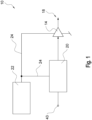
- the RF generator 10 comprises at least one power amplifier (PA) 14 amplifying an RF signal provided by a driver 20 to generate an amplified version of the RF signal at the output 18 as RF output.
- the connection 43 may be used to provide an RF modulated input signal to the driver 20.
- the driver 20 and the power amplifier 14 are supplied by a DC power supply 22, which is connected to the PA 14 and the driver 20 via a busbar 24.
- a DC voltage V busbar is applied to the PA 14 and the driver 20.
- the RF generator 10 according to the present invention is able to provide an amplified RF signal at output 18 with an output power of 2 kW or more, preferably 5 kW or more.
- the RF signal has a frequency of 0.3 - 300 MHz and in particular 13.56 MHz, 27.12 MHz, 40.68 MHz or 60 MHz.
- the envelope of the RF output signal is shaped by changes of the driver output power.
- typical pulse rates are in the range of 1 Hz to 100 kHz and might be up to 1 MHz.
- transients might occur on V busbar , which need to be suppressed.
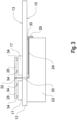
- the RF generator 10 comprises a cooling element 12 built as cold plate, which might be water cooled or cooled by another coolant flowing through channels within the cooling element 12.
- the cooling element 12 comprises an upper surface 13 and a lower surface 15.
- a driver 20 is arranged on the upper surface 13 of the cooling element 12 .
- each power stage 17 may comprise one or more PAs 14, wherein the signals of each PA 14 of one power stage 17 may be combined by a combiner (not shown).
- the output 29 of each power stage 17 is combined in a power combiner 16 and provided to the output coupler 18.
- two DC power supplies 22 are arranged at the lower surface 15 of the cooling element 12.
- the two DC power supplies 22 are connected via a bracket 26 to the busbar 24.
- there might be more or less DC power supplies and/or the one or more DC power supplies may be at least partially arranged at the upper surface 13 of the cooling element 12.
- the DC power supplies 22, the power stages 17, the power combiner 16, and the driver 20 share a common cooling element 12.
- the one or more DC power supplies may not be cooled by a cooling element and may, instead, be cooled by an airstream generated by a fan.
- the DC power supplies 22 are connected to the power stages 17 by a busbar 24.
- the busbar 24 is at least partially built as metal stripe or ribbon.
- the busbar 24 is arranged partially at the lower surface 15 of the cooling element 12 and partially above the upper surface 13 of the cooling element 12 wherein the busbar 24 is routed through an opening 35 in the cooling element from the lower to the upper side of the cooling element.
- the busbar 24 is partially arranged between the DC power supply 22 and the lower surface 15 of the cooling element 12.
- an insulating layer 30 may be arranged between the busbar 24 and the lower surface 15 of the cooling element 12.
- the cooling element 12 may comprise an opening 35 through which the busbar extends towards the upper surface 13 of the cooling element 12. Therein, a substantially vertical section 32 of the busbar 24 extends through the opening 35 and above the power stages 17.
- the busbar 24 is connected to the individual power stages 17 by a connecting PCB 28.
- the connecting PCB 28 is above the power stages 17 and separate therefrom.
- the connecting PCB 28 is connected to the power stages 17 by connectors 34, e. g. metallic bolts, spacers, or standoffs, to supply the V busbar voltage to the power stages 17, i.e the PAs 14.
- connectors 34 e. g. metallic bolts, spacers, or standoffs
- the busbar may be implemented without metallic stripe and only by the connecting PCB 28.
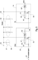
- connection 44 is connected to the one or more DC power supplies 22.
- the connection 43 may be connected to an RF signal source to provide an RF modulated signal to the driver 20.
- a damping network 42 Connected to the busbar 24 is a damping network 42.
- the damping network 42 may be arranged on the individual connecting PCBs 28.
- the damping network 42 is described in more detail with reference to Figure 4 .
- the damping network 42 may be integrated into the busbar 24 by connectors 36 and 37.
- the damping network 42 comprises a plurality of capacitors 40 having the capacitance C 1 , C 2 ,..., C i ,..., C n .
- the sum of the capacitance of all capacitors in the damping network 42, ⁇ i C i is less than 200 ⁇ F, preferably less than 100 ⁇ F and more preferably less than 50 ⁇ F.
- all capacitors 40 are built as ceramic capacitors.
- ceramic capacitors are more reliable and have an increased lifetime compared to electrolyte capacitors.
- such high capacitance could only be achieved with electrolyte capacitors or metal film capacitors, which suffer thermal stress and a reduced lifetime.
- the present invention it is suggested to implement a reduced capacitance of the damping network 42 and thereby enabling the use of more reliable ceramic capacitors without increase of the space of the RF generator 10.
- the time constant is reduced such that the resonances of the damping network 42 are above the operating frequencies of the RF generator 10.
- one or more of the capacitors 40 preferably all of the capacitors 40, are connected in series with damping resistors 38 as depicted in Figure 4 .
- the damping resistors 38 have the resistance R 1 , R 2 , ..., R n , respectively.
- the resistances of the resistors 38 and the capacitances of the capacitors 40 are selected with identical values as follows: R1 3,9 Ohm C1 330 nF R2 3,9 Ohm C2 330 nF R3 3,9 Ohm C3 330 nF R4 3,9 Ohm C4 330 nF R5 3,9 Ohm C5 330 nF R6 3,9 Ohm C6 330 nF R7 3,9 Ohm C7 330 nF R8 3,9 Ohm C8 330 nF
- the capacitances and the resistances of the capacitors 40 and the resistors 38 respectively, have two different values each.
- the resistances and the capacitances are selected as follows: R1 1 Ohm C1 14 nF R2 47 Ohm C2 680 nF R3 1 Ohm C3 14 nF R4 47 Ohm C4 680 nF R5 1 Ohm C5 14 nF R6 47 Ohm C6 680 nF R7 1 Ohm C7 14 nF R8 47 Ohm C8 680 nF
- every capacitor and every resistor may have a different value and may be selected as follows: R1 1 Ohm C1 14 nF R2 2.7 Ohm C2 33 nF R3 4.7 Ohm C3 120 nF R4 12 Ohm C4 270 nF R5 27 Ohm C5 390 nF R6 33 Ohm C6 470 nF R7 47 Ohm C7 680 nF R8 120 Ohm C8 820 nF
- Figures 4 and 5 show only one capacitor 40 and only one resistor 38 for each RC combination, however, the capacitance as well as the resistance of one RC combination can be composed by a combination of more than one capacitor and/or more than one resistor, respectively. Further, although the tables above indicate a specific number of resistors and their resistances as well as a specific number of capacitors and their capacitances, these are only examples and should not be construed in any limiting way.
- the RF generator can fit into a standardized 19/2-inch (241.3-mm) sized housing or into a 19-inch (482.6-mm) sized housing.
- the busbar 24 may be connected to an RF decoupling network 58 which is built as low pass filter which has at least one capacitor 57 connected to ground and which, additionally, may comprise a resistor.
- the capacitance of the capacitor 57 may be less than 1000 nF, preferably less than 500 nF and more preferably less than 250 nF.
- the driver 20 may comprise a MOSFET 52 comprising a drain-gate-feedback connection 46, where the drain-gate-feedback connection 46 comprises at least one capacitor 45.
- the capacitor 45 of the drain-gate-feedback connection 46 may have a capacitance of less than 2000 pF, preferably less than 1000 pF and more preferably less than 100 pF.
- the capacitor 45 may be combined with a resistor 47.
- the resistance of the resistor 47 may be less than 10 kOhm preferably less than 5 kOhm and more preferably 2 kOhm or less.
- the driver 20 is connected to a PA 14 of the power stage 17, wherein in the connection a DC blocking capacitor 48 is arranged.
- the DC blocking capacitor 48 may have a capacitance of less than 10 nF, preferably less than 5 nF, and more preferably less than 2 nF.
- the PA 14 comprises a MOSFET 56, preferably built as LDMOS.
- the MOSFET 56 comprises a drain-gate-feedback connection 51, wherein the drain gate feedback connection 51 may comprise a capacitor 49.
- the capacitor 49 of the drain-gate-feedback connection 51 may have a capacitance of less than 1000 nF, preferably less than 500 nF and more preferably equal to or less than 200 nF.
- the drain-gate-feedback connection 51 may comprise a resistor 50, wherein the resistor 50 may have a resistance of less than 1 kOhm, II preferably less than 800 Ohm and more preferably less than 600 Ohm.
- additional filters 60, 60' may be implemented in order to shape the RF signal.
- additional filters 60, 60' may be implemented in order to shape the RF signal.
- the total capacitance of the damping network 42 is reduced and still sufficiently suppressing transients on the busbar 24 and their effects on the RF output.
- Additional measures can be implemented to provide an undisturbed RF signal at the output of the RF generator. Therein, a deviation between the generated RF output signal and a set point corresponding to the intended RF signal power of less than +/- 5% can be achieved.
Landscapes
- Physics & Mathematics (AREA)
- Engineering & Computer Science (AREA)
- Plasma & Fusion (AREA)
- Chemical & Material Sciences (AREA)
- Analytical Chemistry (AREA)
- Amplifiers (AREA)
- Control Of Voltage And Current In General (AREA)
Description
- The present invention relates to a radio frequency (RF) generator in particular for a plasma application.
- Plasma processing is a very versatile and precise technique to modify the surfaces of materials, in particular in the manufacturing of semiconductor chips. In plasma processing systems, RF power signals are used to excite gaseous compounds such that free electrons and ions are formed. Depending on a variety of process parameters, the plasma composition, i. e. the amount of ions, electrons, neutrals, and various radicals can be controlled precisely. Such plasma processes are used multiple times in semiconductor production, preferably for the deposition of layers onto a semiconductor wafer or for etching the surface of a semiconductor wafer, both with high uniformity and very precisely over the entire surface.
- Plasma process tools are typically operated with RF power signals at frequencies in the range from 0.3 MHz to 300 MHz and at power levels of 50 W and higher, preferably 500 W and higher.
- The use of pulse-mode operation to modulate the envelope of the RF power signal has several advantages, in particular, the amount of power dissipated within the semiconductor wafer over a certain time period can be adjusted such that detrimental effects on the wafer or the involved materials are prevented. In addition, the ratio of the different active species can be varied by the power modulation such that, during the various pulsing stages, different reactive species are dominant. This allows to tailor the chemical processes which occur at the wafer surface.
- For an RF generator, pulse-mode operation is challenging. Typical pulse rates are in the range of 1 Hz to 100 kHz, but also up to 1 MHz. In consequence, the output of the RF generator has to be modulated accordingly, for example, a sequence of different power levels has to be adjusted in a repeating pattern. The rapid changes of output power can cause internal fluctuations which affect the stability of the DC power which is provided to all parts of the circuit.
- Ideally, the DC supply in an RF generator provides a stable settable voltage for an RF power amplifier (PA) input. In fast pulse-mode operation, the DC power supply is operated at a constant set point and provides power to the PA which generates the carrier signal. The modulation of the output power can be done via the driver circuit as a modulation of the gate voltage of the PA.
- The DC voltage (Vbusbar) is distributed via a rail ("busbar") and feeds the driver circuit and the PAs of the RF generator. Ideally, the output wave form of an RF generator in pulse-mode operation would be an amplified copy of the PA input, i. e. rectangular edges when the power level is changed with very fast rise and fall times.
- In reality, a stray impedance is present between the DC power supply and the PAs. When the required output current suddenly changes by the modulation, e. g. during RF turn-on and turn-off, when changing the power level, or periodically in pulse-mode operation, transient voltage excursions and oscillations occur on the DC voltage Vbusbar at the inputs of driver and PA, generating undesired additional signal modulation, for example reduced rise and fall times, over- and undershoots.
- The acceptable tolerances for over- and undershoots and the required rise and fall times for power level changes are typically given by the user of the RF generator. Additional boundary conditions and limits on components may be required to ensure reliable, stable, and safe operation of DC supply and PA.
- Therefore, an optimization of the components for stabilizing the RF generator's output to several boundary conditions is required to fulfill the output signal specifications.
- The standard solution to avoid Vbusbar transients on the busbar is the use of banks of electrolyte capacitors with large capacitance such that all voltage fluctuations are completely suppressed. Therein, a total capacitance of more than 1000 µP or even 2000 µP and higher is implemented usually by electrolyte capacitors. Therein, electrolyte capacitors are an easy way to provide such a high capacitance in a relatively compact way.
- However, electrolyte capacitors are very sensitive in terms of reliability. To operate them for several years without failure (as is required in semiconductor production) requires that their operating temperature be kept below specified limits which means that cooling is required. Due to the geometrical shape of such capacitors, they cannot be appropriately mounted on a cooling plate, and only air cooling via fans is possible.
- Power RF generators above 2 kW are typically water-cooled, and all circuit parts which require cooling are arranged on a cooling plate through which water circulates. For such power generators, the use of electrolyte capacitors would require additional air cooling which comes at additional cost and space consumption. Also, for power levels above 2 kW the required number of electrolyte capacitors can typically only be fit into a full 19-inch (482.6-mm) wide housing, but not into a 19/2-inch (241.3-mm) wide housing, since efficient air cooling requires a certain spacing of the capacitors.
- Due to their particularly large capacitance values, electrolyte capacitors can only be replaced by a much larger number of alternative capacitors. Such alternatives have smaller capacitances. However, due to the required large number, they need much more space than electrolyte capacitors of a similar capacitance.
- There is therefore a need to avoid the use of electrolyte capacitors banks in RF generators, but at the same time to fit the power RF generator with high output powers into a 19/2-inch (241.3-mm) wide housing.
-
US 2014/232483 A1 describes a combiner for an RF amplifier comprising wiring and a transmission line transformer. -
EP 3 745 835 A1 describes a generator that includes a housing, a high-power circuit including a power amplifier, and a low-power circuit. An air flow guidance plate divides the housing into at least two compartments including a high-power compartment and a low-power compartment. The high-power circuit is disposed within the high-power compartment and the low-power circuit is disposed within the low-power compartment. -
US 2020/395901 A1 describes a multi-stage system of a radio frequency (RF) power amplifier. Fluid cooling is incorporated directly into the power amplifier (PA) module design. Therein, a PA module includes a circuit board, RF circuit components, a ground plane, and a cooling plate having one or more cooling channels to receive a cooling fluid. The cooling channels are positioned to dissipate heat from the RF circuit components through the ground plane. The PA module may also include RF bias and power electronics within a housing for the PA module without requiring an external control board or power conversion electronics. -
US 5 332 979 A describes a compact RF generator system.US 2003/142513 A1 discloses the use of a a damping circuit, comprising a damping resistor and a damping capacitor, to reduce or eliminate the oscillatory ringing and overshoot that may develop in an output voltage. - Thus, it is an objective of the present invention to provide an RF generator, which overcomes the drawbacks of the prior art.
- The problem is solved by a radio frequency (RF) generator according to claim 1.
- The present invention provides an RF generator, in particular for plasma applications. The RF generator generates an RF output and comprises at least one cooling element having an upper surface and a lower surface. Therein, the cooling element may be built as cold plate including one or more channels or pipes through which a coolant can flow in order to cool the cold plate. Alternatively, the cooling element may be built as heat sink, which may be cooled by an airstream. Further, the RF generator comprises at least one DC power supply. Preferably the RF generator comprises two or more DC power supplies. Therein, the one or more DC power supplies can be connected to the cooling element and cooled via the cooling element. Alternatively, the DC power supplies may be separated from the cooling element and may be cooled by an independent cooling element, e.g. cooled by an airstream generated by an independent fan.
- The RF generator comprises at least one power stage to amplify an RF signal, wherein the power stage is connected to an upper surface of the at least one cooling element. The power stage comprises one or more power amplifiers (PAs). If there is more than one power stage, the RF generator may comprise a power combiner in order to combine the amplified RF signal of the more than one power stages. In addition, or alternatively, each power stage may comprise more than one PA, wherein the amplified RF signal of each PA is combined by a combiner, which may be part of the power stage or an individual component. Therein, due to connecting the at least one power stage to the cooling element the at least one power stage is efficiently cooled by the cooling element.
- The RF generator further comprises a driver to supply the PA of the at least one power stage, wherein the driver is connected to the upper surface of the at least one cooling element for cooling the driver.
- Therein, the at least one DC power supply is connected by a busbar with the PA and the driver, wherein a DC voltage Vbusbar is supplied to the PA and the driver via the busbar. The busbar comprises a damping network comprising a plurality of capacitors connected between ground and the busbar and configured to shape transients on Vbusbar. Thus, by the damping network, transient voltage excursions and oscillations on Vbusbar can be reduced in order to provide a reliable, stable and safe operation of the DC power supply, PA, and any other component. At the same time, it is possible to meet the requirements with respect to acceptable tolerances for the required rise and fall times for power level changes Preferably, the busbar is at least partially built as PCB connecting the DC power supply with the PA and the driver. More preferably, the busbar is completely provided by a PCB.
- Preferably, the busbar is at least partially built as metal bar or stripe. Thus, the busbar may be built as a combination of a PCB and the metal bar or stripe. Therein, the metal bar or stripe may have a width larger than the height of the stripe, preferably by a factor of 10 and more preferably by a factor of 20. In particular, the metal stripe may have a height or thickness of between 0.5 mm and 3 mm and a width of between 15 and 30 mm.
- Preferably, the busbar comprises an inductance of 50nH or less and, preferably, 40 nH or less. By these values, the effect of transient voltage excursions and oscillations occurring on the DC voltage Vbusbar at the inputs of driver and PA can be reduced.
- Preferably, the damping network capacitors are built as ceramic capacitors. Ceramic capacitors have the advantage of an increased lifetime compared to electrolyte capacitors or metal film capacitors, thereby also increasing the lifetime of the RF generator and the reliability of operation. In addition, less cooling or no additional cooling may be required for ceramic capacitors due to their thermal endurance.
- Preferably, the ceramic capacitors are connected to the cooling element for cooling. Thus, efficient cooling is possible due to use of the ceramic capacitors. Alternatively, if the ceramic capacitors cannot be connected directly to the cooling element, an indirect connection to the cooling element can be implemented. This indirect connection may include an array of vias connecting the solder pads of the ceramic resistors to similar areas on the bottom side of the PCB to which the ceramic capacitors are attached. Thus, thermal losses are spread over a larger area of the PCB. In addition, thermally conductive metal standoffs, spacers, or bolts to which the PCB is screwed may thermally connect specific areas for cooling on the bottom side of the PCB to the cooling element. Alternatively or additionally, convection air cooling might be used to provide cooling.
- Preferably, the sum or total capacitance of all capacitors in the damping network is less than 200 µF, preferably less than 100 µF, more preferably less than 50 µF, even more preferably less than 10 µF and most preferably less than 5 µF. In order to provide a compact size of the RF generator and, in particular, to fit the RF generator in a 19/2-inch (241.3-mm) sized housing, it is desirable to reduce the space required by the capacitors of the damping network. At the same time, by reducing the capacitance of the damping network, the current provided by the DC supply can be limited when loading the capacitors of the damping network.
- Due to the reduced capacitance of the damping network, the time constant of the LC network of busbar inductance and capacitance of the damping network may be below 10 µs.
- Thus, the resonance is shifted to above the pulsing frequency of the RF generator, wherein in the prior art when using capacitors with a total capacitance of 1000 µF or more, the resonance frequency was within the range of the pulsing frequency of the RF generator. For example, for a busbar inductance in the range of 20 nH to 50 nH, and a state-of-the-art damping network with electrolyte capacitors of a total capacitance of 1 to 5 mF, the resonance frequency would be in the range of 10 to 35 kHz, which is within the range of typically used pulse rates of 1 Hz to 100 kHz. In contrast, for the much smaller capacitances in the damping network according to this invention, e. g. 2 to 10 µF, the resonance frequency would be between 220 kHz and 800 kHz, which is much higher than the usual pulse rates.
- When the RF power is suddenly changed from one level to another in pulse-mode operation, the time constant for over- and undershoots is derived from the resonance frequency of the busbar inductance and the damping network capacitance. In consequence, for the example above, the state-of-the-art damping network with electrolyte capacitors would have a time constant in the range of 30 to 100 microseconds, whereas the solution according to this invention would have a time constant of 1 to 4 microseconds.
- For the electrolyte capacitor solution, such over- and undershoots with long time constant can be compensated by the regulation loop which controls the RF output power. However, this is not possible in all cases depending on the required speed of the regulation. In addition, if the electrolyte capacitors are operated with pulse frequencies in the range of the resonances described above, an increased ripple current results which causes thermal losses and severely impacts the lifetime of the electrolyte capacitors. This is a particular disadvantage of the state-of-the-art solution in an RF generator which is operated in pulse mode compared to the damping network with much smaller capacitances according to this invention.
- In the solution according to this invention with strongly reduced capacitance which can be realized by ceramic capacitors, the lifetime issue of electrolyte capacitors is avoided. Due to the short time constant of over- and undershoots, they are always much shorter than the pulse length and in the vicinity of the rising and falling edges of the pulse pattern. The combination of resistances and capacitances of the RC damping network is specifically designed to keep the excursions of over- and undershoots within the specified deviations from the power set value.
- Due to the reduced total capacitance of the damping network, the damping network can be realized solely by ceramic capacitors increasing the reliability and lifetime of the RF generator.
- Preferably, the one or more capacitors in the damping network comprise a damping resistor or are connected to a damping resistor in series to create an RC combination. Thus, by the damping resistor, damping of transients on Vbusbar is achieved.
- Preferably, two or more damping resistors have different resistance values. Preferably, all damping resistors have different resistance values. Alternatively, all damping resistors have the same resistance value.
- Preferably, the capacitors of the damping network comprise different capacitances. Therein, at least two capacitors of the damping network may have a different capacitance or each of the capacitors of the damping network has a different capacitance. Thus, transients on different time scales can be efficiently damped.
- Preferably, the damping network comprises RC combinations with different time constants. Thus, the time constants by the combination of the capacitor and the damping resistor are different for at least two RC combinations or are different for each of the RC combination of the damping network. Therein, the RC combinations with decreased capacitance comprise a decreased resistance. In other words, the smaller the capacitance of the capacitor of the RC combination the smaller the resistance of the resistor of the RC combination.
- Preferably, the damping network is arranged on a separate PCB, wherein preferably the damping network comprises one PCB for each power stage. Therein, the PCB may be separate from the driver PCB and/or the power stage. Thus, by use of a separate PCB, arrangement of the damping network within the housing of the RF generator is facilitated in order to provide a compact RF generator. In particular, stacking of two or more PCBs in a three-dimensional arrangement, may be used to achieve a compact arrangement which is compatible with a 19/2-inch (241.3-mm) wide housing of the RF generator.
- Preferably, the PCB of the damping network is arranged above the power stage. The PCB is thus placed relative to the power stage opposite to the cooling element. In particular, the PCB is placed in a distance from the power stage and connected to the power stage by one or more connectors such as metallic bolts, spacers, or standoffs. Thereby, a compact arrangement of the damping network is achieved and connection with the power stage is facilitated.
- Preferably, the DC power supply is connected to the same cooling element as the power stage and/or the driver. Thus, a compact RF generator is built, and the required number of cooling elements may be reduced. Alternatively, the DC power supply is arranged on a separate cooling element. Alternatively, the DC power supply is not connected to any cooling element of the RF generator and may be cooled by an air stream generated by a fan of the DC power supply. Preferably, the DC power supply is arranged at the lower surface of the at least one cooling element.
- Preferably, the at least one cooling element comprises an opening to feed the busbar from the lower surface to the upper surface of the cooling element. Preferably, the busbar is connected to the lower surface of the cooling element, wherein an insulating layer is arranged between the busbar and the at least one cooling element. By using an electrically insulating, but thermally conducting layer between the busbar and the at least one cooling element, cooling of the busbar is facilitated.
- Preferably, the RF generator comprises more than one DC power supply, wherein all DC power supplies are connected to the same busbar. Thus, by using more than one DC power supply the available output power of the RF generator can be increased.
- Preferably, the RF generator generates more than 2 kW RF output and preferably more than 5 kW.
- Preferably, the RF generator is arranged inside a housing, wherein the housing has preferably a standardized 19/2-inch (241.3-mm) size or a 19-inch (482.6-mm) size. Thus, a compact built RF generator is provided.
- Preferably, the busbar comprises an RF decoupling network, wherein the RF decoupling network comprises one or more capacitors. Therein, the decoupling network acts as a low pass filter. In particular, the capacitors are connected to ground. Preferably, the capacitors have a total, i e. combined, capacitance of less than 1000 nF, preferably less than 500 nF and more preferably less than 250 nF.
- Preferably, the driver comprises a MOSFET having a drain-gate-feedback connection, wherein the drain-gate-feedback connection comprises a capacitor in order to suppress or reduce transients of Vbusbar to the gate. Preferably, the capacitor comprises a capacitance of less than 2000 pF, preferably less than 1000 pF and more preferably less than 100 pF.
- Preferably, the PA comprises a MOSFET, in particular built as LDMOS (laterally diffused metal oxide semiconductor) having a drain-gate-feedback connection, wherein the drain-gate-feedback connection comprises a capacitor to reduce transients of Vbusbar to the gate. In particular, the capacitor has a capacitance of less than 2000 nF, preferably less than 500 nF and more preferably equal to or less than 200 nF.
- Preferably, the driver comprises an output network comprising a DC blocking capacitor having a capacitance of preferably less than 10 nF, preferably less than 5 nF and more preferably less than 2 nF.
- Therein, the output network may be arranged between the driver and the PA, in particular the gate of the PA MOSFET.
- Preferably, the output network of the driver comprises a series RC circuit parallel to the DC blocking capacitor. Therein, the series RC circuit comprises a resistor and a capacitor connected in series. Preferably, the resistor has a resistance between 0.5 kOhm and 1.5 kOhm and the capacitor of the RC circuit has a capacitance between 0.5 nF and 2 nF.
- Preferably, the RF output comprises a rise- and fall-time of less than 1.5 µs and preferably less than 1 µs.
- Therein, the rise and fall times are defined by a 10% to 90% change of full power up or a 90% to 10% change of full power down, e. g. for a 1000 W to 100 W power change, the time period for going from 910 W to 190 W is below 1.5 µs and preferably below 1 µs.
- Preferably, the output RF power deviates from a setpoint within +/- 5%. This means that transient output power over- and undershoots stay within +/- 5% of the set power.
- Thus, by the RF generator of the present invention a damping network is used in order to reduce transients on the Vbusbar voltage provided by the DC power supply due to a stray impedance of the busbar. Therein, the damping network only comprises ceramic capacitors increasing the lifetime of the RF generator.
- However, in order to further compensate for the reduced capacitance of the ceramic capacitors, compared for example to electrolyte capacitors, additional measures may be implemented in the RF generator to avoid/reduce transients and their effects on the amplified RF output. Such measures may include one or more of an optimized RF decoupling network, optimized drain-gate-feedback connections in the driver and/or the PA, or an optimized DC blocking capacitor between the driver and the PA. Thus, acceptable tolerances for over- and undershoots and the required rise and fall times for power level changes of the RF generator can be met. Additional boundary conditions and limits on components may be fulfillable to ensure reliable, stable, and safe operation of DC supply and PA.
- In the following the present invention is described in more detail with reference to the accompanying figures.
- The figures show:
- Figure 1
- a schematic representation of an RF generator,
- Figure 2
- a detailed representation of an RF generator according to the present invention in top view,
- Figure 3
- a side view of the RF generator according to
Figure 2 , - Figure 4
- a detailed representation of the damping network and
- Figure 5
- a schematic RF generator circuit according to the present invention.
- Referring to
Figure 1 showing aschematic RF generator 10. TheRF generator 10 comprises at least one power amplifier (PA) 14 amplifying an RF signal provided by adriver 20 to generate an amplified version of the RF signal at theoutput 18 as RF output. Theconnection 43 may be used to provide an RF modulated input signal to thedriver 20. Therein, thedriver 20 and thepower amplifier 14 are supplied by aDC power supply 22, which is connected to thePA 14 and thedriver 20 via abusbar 24. By the busbar 24 a DC voltage Vbusbar is applied to thePA 14 and thedriver 20. Therein, theRF generator 10 according to the present invention is able to provide an amplified RF signal atoutput 18 with an output power of 2 kW or more, preferably 5 kW or more. The RF signal has a frequency of 0.3 - 300 MHz and in particular 13.56 MHz, 27.12 MHz, 40.68 MHz or 60 MHz. Therein, in pulse-mode operation of theRF generator 10, the envelope of the RF output signal is shaped by changes of the driver output power. Therein, typical pulse rates are in the range of 1 Hz to 100 kHz and might be up to 1 MHz. By this pulse-mode operation, internal fluctuations may occur, which affect the stability of the DC power supply and/or other components of the RF generator. In particular, transients might occur on Vbusbar, which need to be suppressed. - Referring to
Figures 2 and3 showing anRF generator 10 in top view and side view, respectively. InFig. 2 , modules and components with solid-line boundaries are located on or above the upper side of thecooling element 12, whereas modules and components with dashed-line boundaries are located on or below the lower side of thecooling element 12. In the example ofFigure 2 theRF generator 10 comprises acooling element 12 built as cold plate, which might be water cooled or cooled by another coolant flowing through channels within thecooling element 12. As indicated inFig. 2 and3 , thecooling element 12 comprises anupper surface 13 and alower surface 15. On theupper surface 13 of the cooling element 12 adriver 20 is arranged. In addition, in the example ofFigures 2 and3 , twopower stages 17 are arranged to amplify the RF signal from thedriver 20. Therein, eachpower stage 17 may comprise one ormore PAs 14, wherein the signals of eachPA 14 of onepower stage 17 may be combined by a combiner (not shown). Theoutput 29 of eachpower stage 17 is combined in apower combiner 16 and provided to theoutput coupler 18. - In the example of
Figures 2 and3 , two DC power supplies 22 are arranged at thelower surface 15 of thecooling element 12. The two DC power supplies 22 are connected via abracket 26 to thebusbar 24. Alternatively, in another embodiment there might be more or less DC power supplies and/or the one or more DC power supplies may be at least partially arranged at theupper surface 13 of thecooling element 12. Thus, in the example ofFigures 2 and3 , the DC power supplies 22, the power stages 17, thepower combiner 16, and thedriver 20 share acommon cooling element 12. Alternatively, there might be more than onecooling element 12, wherein for example the DC power supplies 22 may be arranged on a separate cooling element. Alternatively, the one or more DC power supplies may not be cooled by a cooling element and may, instead, be cooled by an airstream generated by a fan. - The DC power supplies 22 are connected to the power stages 17 by a
busbar 24. In the example ofFigures 2 and3 , thebusbar 24 is at least partially built as metal stripe or ribbon. Thebusbar 24 is arranged partially at thelower surface 15 of thecooling element 12 and partially above theupper surface 13 of thecooling element 12 wherein thebusbar 24 is routed through anopening 35 in the cooling element from the lower to the upper side of the cooling element. In particular, thebusbar 24 is partially arranged between theDC power supply 22 and thelower surface 15 of thecooling element 12. In order to avoid short circuits between thebusbar 24 and thecooling element 12, an insulatinglayer 30 may be arranged between thebusbar 24 and thelower surface 15 of thecooling element 12. In order to route thebusbar 24 from thelower surface 15 to theupper surface 13 of thecooling element 12, thecooling element 12 may comprise anopening 35 through which the busbar extends towards theupper surface 13 of thecooling element 12. Therein, a substantiallyvertical section 32 of thebusbar 24 extends through theopening 35 and above the power stages 17. - Preferably, the
busbar 24 is connected to the individual power stages 17 by a connectingPCB 28. Therein, the connectingPCB 28 is above the power stages 17 and separate therefrom. The connectingPCB 28 is connected to the power stages 17 byconnectors 34, e. g. metallic bolts, spacers, or standoffs, to supply the Vbusbar voltage to the power stages 17, i.e thePAs 14. Therein, in particular for eachpower stage 17 anindividual connecting PCB 28 is implemented. - In an embodiment where the
DC power supply 22 is arranged on theupper side 13 of thecooling element 12 or laterally side by side to theupper side 13 of the cooling element 12 (i. e. with the DC output at the same side as the power stages 17, but may be arranged on different cooling elements or without cooling element), the busbar may be implemented without metallic stripe and only by the connectingPCB 28. - Referring to
Figure 5 showing a simplified representation of the circuit of theRF generator 10. Therein, theconnection 44 is connected to the one or more DC power supplies 22. Theconnection 43 may be connected to an RF signal source to provide an RF modulated signal to thedriver 20. Connected to thebusbar 24 is a dampingnetwork 42. The dampingnetwork 42 may be arranged on theindividual connecting PCBs 28. The dampingnetwork 42 is described in more detail with reference toFigure 4 . The dampingnetwork 42 may be integrated into thebusbar 24 byconnectors network 42 comprises a plurality ofcapacitors 40 having the capacitance C1, C2,..., Ci,..., Cn. Therein, the sum of the capacitance of all capacitors in the dampingnetwork 42, Σ i C i , is less than 200 µF, preferably less than 100 µF and more preferably less than 50 µF. - In particular, all
capacitors 40 are built as ceramic capacitors. Therein, ceramic capacitors are more reliable and have an increased lifetime compared to electrolyte capacitors. Usually, it would be intended to increase the capacitance of the dampingnetwork 42 in order to suppress transients on the Vbusbar voltage. With higher capacitance, the required loss to suppress resonances can be decreased. Therefore, the maximum possible capacitance within the available space would be used to keep the heat generated as low as possible. However, such high capacitance could only be achieved with electrolyte capacitors or metal film capacitors, which suffer thermal stress and a reduced lifetime. Thus, by the present invention, it is suggested to implement a reduced capacitance of the dampingnetwork 42 and thereby enabling the use of more reliable ceramic capacitors without increase of the space of theRF generator 10. By the reduced capacitance of thecapacitors 40 of the dampingnetwork 42, the time constant is reduced such that the resonances of the dampingnetwork 42 are above the operating frequencies of theRF generator 10. In order to damp transients on the Vbusbar voltage and suppress over- and undershoots, one or more of thecapacitors 40, preferably all of thecapacitors 40, are connected in series with dampingresistors 38 as depicted inFigure 4 . Therein, the dampingresistors 38 have the resistance R1, R2, ..., Rn, respectively. - Therein, for example all capacitances C1, ..., Cn might be the same or different. Similar, all resistances R1, ..., Rn might be the same or different.
- In a first example the resistances of the
resistors 38 and the capacitances of thecapacitors 40 are selected with identical values as follows:R1 3,9 Ohm C1 330 nF R2 3,9 Ohm C2 330 nF R3 3,9 Ohm C3 330 nF R4 3,9 Ohm C4 330 nF R5 3,9 Ohm C5 330 nF R6 3,9 Ohm C6 330 nF R7 3,9 Ohm C7 330 nF R8 3,9 Ohm C8 330 nF - In another example, the capacitances and the resistances of the
capacitors 40 and theresistors 38, respectively, have two different values each. In one example, the resistances and the capacitances are selected as follows:R1 1 Ohm C1 14 nF R2 47 Ohm C2 680 nF R3 1 Ohm C3 14 nF R4 47 Ohm C4 680 nF R5 1 Ohm C5 14 nF R6 47 Ohm C6 680 nF R7 1 Ohm C7 14 nF R8 47 Ohm C8 680 nF - Thereby, by the different RC combinations, transients on different time scales can be efficiently damped. Therein, in particular the smaller the capacitance of the
capacitor 40 of an RC combination, the smaller the resistance of the dampingresistor 38 can be selected. In another example, every capacitor and every resistor may have a different value and may be selected as follows:R1 1 Ohm C1 14 nF R2 2.7 Ohm C2 33 nF R3 4.7 Ohm C3 120 nF R4 12 Ohm C4 270 nF R5 27 Ohm C5 390 nF R6 33 Ohm C6 470 nF R7 47 Ohm C7 680 nF R8 120 Ohm C8 820 nF - Although
Figures 4 and5 show only onecapacitor 40 and only oneresistor 38 for each RC combination, however, the capacitance as well as the resistance of one RC combination can be composed by a combination of more than one capacitor and/or more than one resistor, respectively. Further, although the tables above indicate a specific number of resistors and their resistances as well as a specific number of capacitors and their capacitances, these are only examples and should not be construed in any limiting way. - Due to implementing the damping
network 42 according toFigure 4 , efficient damping of transients of the Vbusbar voltage is feasible with one or more time constants. - By reducing the capacitance of the damping
network 42, the required space for the ceramic capacitors is maintained or even reduced in comparison to the use of electrolyte capacitors. Thus, the RF generator can fit into a standardized 19/2-inch (241.3-mm) sized housing or into a 19-inch (482.6-mm) sized housing. - In order to be able to further reduce the effects of transients onto the RF output, the
busbar 24 may be connected to anRF decoupling network 58 which is built as low pass filter which has at least onecapacitor 57 connected to ground and which, additionally, may comprise a resistor. Therein, the capacitance of thecapacitor 57 may be less than 1000 nF, preferably less than 500 nF and more preferably less than 250 nF. - The
driver 20 may comprise aMOSFET 52 comprising a drain-gate-feedback connection 46, where the drain-gate-feedback connection 46 comprises at least onecapacitor 45. Therein, thecapacitor 45 of the drain-gate-feedback connection 46 may have a capacitance of less than 2000 pF, preferably less than 1000 pF and more preferably less than 100 pF. - The
capacitor 45 may be combined with aresistor 47. The resistance of theresistor 47 may be less than 10 kOhm preferably less than 5 kOhm and more preferably 2 kOhm or less. - The
driver 20 is connected to aPA 14 of thepower stage 17, wherein in the connection aDC blocking capacitor 48 is arranged. Therein, theDC blocking capacitor 48 may have a capacitance of less than 10 nF, preferably less than 5 nF, and more preferably less than 2 nF. - The
PA 14 comprises aMOSFET 56, preferably built as LDMOS. TheMOSFET 56 comprises a drain-gate-feedback connection 51, wherein the draingate feedback connection 51 may comprise acapacitor 49. Therein, thecapacitor 49 of the drain-gate-feedback connection 51 may have a capacitance of less than 1000 nF, preferably less than 500 nF and more preferably equal to or less than 200 nF. - Further, the drain-gate-
feedback connection 51 may comprise aresistor 50, wherein theresistor 50 may have a resistance of less than 1 kOhm, II preferably less than 800 Ohm and more preferably less than 600 Ohm. - In the output of the
power stage 14 as well as in the output of thedriver 20additional filters 60, 60' may be implemented in order to shape the RF signal. Thus, according to the present invention, in order to useceramic capacitors 40 in the dampingnetwork 42 without increase of the required space, the total capacitance of the dampingnetwork 42 is reduced and still sufficiently suppressing transients on thebusbar 24 and their effects on the RF output. Additional measures can be implemented to provide an undisturbed RF signal at the output of the RF generator. Therein, a deviation between the generated RF output signal and a set point corresponding to the intended RF signal power of less than +/- 5% can be achieved. - By the solution of the present invention, reliable and more stable operation over a longer lifetime of the RF generator can be achieved. Transient overvoltages at the included MOSFETs are kept within safe operational limits and driver as well as PAs can be operated in a stable operating window.
Claims (17)
- Radiofrequency, RF, generator (10), arranged to generate an RF output in particular for a plasma application, comprising:at least one cooling element (12) having an upper surface (13) and a lower surface (15);at least one DC power supply (22);at least one power stage (17) arranged to amplify an RF signal and connected to the upper surface (13) of the at least one cooling element (12), wherein the power stage (17) comprises one or more power amplifiers (14);a driver (20) arranged to supply the power amplifier (14) of the at least one power stage (17), wherein the driver (20) is connected to the upper surface (13) of the at least one cooling element (12); andwherein the at least one DC power supply (22) is connected by a busbar (24) with the power amplifier (14) and the driver (20), wherein the at least one DC power supply (22) is arranged to supply a DC voltage Vbusbar to the power amplifier (14) and the driver (20) via the busbar (24);characterized in thatthe busbar (24) comprises a damping network (42) comprising a plurality of capacitors (40) connected between ground and the busbar (24) and configured to shape transients on Vbusbar.
- RF generator according to claim 1, further characterized in that the damping network capacitors (40) are built as ceramic capacitors.
- RF generator according to any of claims 1 or 2, further characterized in that the sum of the capacitances of all capacitors (40) in the damping network (42) is less than 200 pF, preferably less than 100 µF and more preferably less than 50 µF.
- RF generator according to any of claims 1 to 3, further characterized in that one or more of the capacitors (40) in the damping network (42) comprise a damping resistor (38) or are connected to a damping resistor (38) in series to create an RC combination.
- RF generator according to claim 4, further characterized in that two or more damping resistors (38) have different resistance values.
- RF generator according to claim 4 or 5, further characterized in that the damping network (42) comprises RC combinations with different time constants.
- RF generator according to any of claims 1 to 6, further characterized in that the damping network (42) is arranged on a separate PCB (28), wherein preferably the damping network (42) comprises one PCB (28) for each power stage (17).
- RF generator according to claim 7, further characterized in that the PCB (28) of the damping network (42) is arranged above the power stage (17).
- RF generator according to any of claims 1 to 8, further characterized in that the DC power supply (22) is arranged at the lower surface (15) of the at least one cooling element (12).
- RF generator according to claim 9, wherein the at least one cooling element (12) comprises an opening (35) to feed the busbar (24) from the lower surface (15) to the upper surface (13).
- RF generator according to claim 9 or 10, further characterized in that the busbar (24) is connected to the lower surface (15) of the at least one cooling element (12), wherein an insulating layer (30) is arranged between the busbar (24) and the at least one cooling element (12).
- RF generator according to any of claims 1 to 11, arrangeable inside a housing, wherein the housing has preferably a standardized 19/2-inch (241.3-mm) size or a 19-inch (482.6-mm) size.
- RF generator according to any of claims 1 to 12, further characterized in that the busbar (24) comprises an RF decoupling network (58), wherein the RF decoupling network comprises one or more capacitors (57) having a total capacitance of less than 1000 nF, preferably less than 500 nF, and more preferably less than 250 nF.
- RF generator according to any of claims 1 to 13, further characterized in that the driver (20) comprises a MOSFET (52) having a drain-gate-feedback connection (46), wherein the drain-gate-feedback connection (46) comprises a capacitor (45) having a capacitance of less than 2000 pF, preferably less than 1000 pF and more preferably less than 100 PF.
- RF generator according to any of claims 1 to 14, further characterized in that the power amplifier (14) comprises a MOSFET (56), preferably an LDMOS, having a drain-gate-feedback connection (51), wherein the drain-gate-feedback connection (51) comprises a capacitor (49) having a capacitance of less than 1000 nF, preferably less than 500 nF and more preferably equal to or less than 200 nF.
- RF generator according to any of claims 1 to 15, further characterized in that the driver (20) comprises an output network comprising a DC blocking capacitor (48) having a capacitance of less than 10 nF, preferably less than 5 nF and more preferably less than 2 nF.
- RF generator according to claim 16, further characterized in that the output network comprises a series RC circuit in parallel to the DC blocking capacitor (48), wherein preferably the resistor has a resistance between 0.5 kOhm and 1.5 kOhm and the capacitor of the RC circuit has a capacitance between 0.5 nF and 2 nF.
Priority Applications (6)
| Application Number | Priority Date | Filing Date | Title |
|---|---|---|---|
| EP22206909.8A EP4369377B1 (en) | 2022-11-11 | 2022-11-11 | Radio frequency generator |
| TW112130639A TW202420393A (en) | 2022-11-11 | 2023-08-15 | Radio frequency generator |
| KR1020257015332A KR20250105383A (en) | 2022-11-11 | 2023-09-11 | radio frequency generator |
| JP2025522251A JP2025537088A (en) | 2022-11-11 | 2023-09-11 | High Frequency Generator |
| PCT/EP2023/074896 WO2024099613A1 (en) | 2022-11-11 | 2023-09-11 | Radio frequency generator |
| CN202380077955.4A CN120167077A (en) | 2022-11-11 | 2023-09-11 | RF Generator |
Applications Claiming Priority (1)
| Application Number | Priority Date | Filing Date | Title |
|---|---|---|---|
| EP22206909.8A EP4369377B1 (en) | 2022-11-11 | 2022-11-11 | Radio frequency generator |
Publications (2)
| Publication Number | Publication Date |
|---|---|
| EP4369377A1 EP4369377A1 (en) | 2024-05-15 |
| EP4369377B1 true EP4369377B1 (en) | 2024-12-25 |
Family
ID=84358744
Family Applications (1)
| Application Number | Title | Priority Date | Filing Date |
|---|---|---|---|
| EP22206909.8A Active EP4369377B1 (en) | 2022-11-11 | 2022-11-11 | Radio frequency generator |
Country Status (6)
| Country | Link |
|---|---|
| EP (1) | EP4369377B1 (en) |
| JP (1) | JP2025537088A (en) |
| KR (1) | KR20250105383A (en) |
| CN (1) | CN120167077A (en) |
| TW (1) | TW202420393A (en) |
| WO (1) | WO2024099613A1 (en) |
Families Citing this family (1)
| Publication number | Priority date | Publication date | Assignee | Title |
|---|---|---|---|---|
| EP4307338B1 (en) * | 2022-07-12 | 2024-11-27 | Comet AG | Radio frequency generator |
Family Cites Families (5)
| Publication number | Priority date | Publication date | Assignee | Title |
|---|---|---|---|---|
| DE4104064A1 (en) * | 1991-02-11 | 1992-08-13 | Elektronische Anlagen Gmbh | High power LC filter e.g. for Rf generator - has coils surrounded by magnetic cores with large surface contacts to filter housing |
| US6930893B2 (en) * | 2002-01-31 | 2005-08-16 | Vlt, Inc. | Factorized power architecture with point of load sine amplitude converters |
| US9093731B2 (en) * | 2013-02-21 | 2015-07-28 | Empower RF Systems, Inc. | Combiner for an RF power amplifier |
| GB2584117A (en) * | 2019-05-22 | 2020-11-25 | Comet Ag | Generator |
| US11050394B2 (en) * | 2019-06-14 | 2021-06-29 | Tokyo Electron Limited | Modules, multi-stage systems, and related methods for radio frequency power amplifiers |
-
2022
- 2022-11-11 EP EP22206909.8A patent/EP4369377B1/en active Active
-
2023
- 2023-08-15 TW TW112130639A patent/TW202420393A/en unknown
- 2023-09-11 CN CN202380077955.4A patent/CN120167077A/en active Pending
- 2023-09-11 JP JP2025522251A patent/JP2025537088A/en active Pending
- 2023-09-11 WO PCT/EP2023/074896 patent/WO2024099613A1/en not_active Ceased
- 2023-09-11 KR KR1020257015332A patent/KR20250105383A/en active Pending
Also Published As
| Publication number | Publication date |
|---|---|
| TW202420393A (en) | 2024-05-16 |
| EP4369377A1 (en) | 2024-05-15 |
| WO2024099613A1 (en) | 2024-05-16 |
| KR20250105383A (en) | 2025-07-08 |
| JP2025537088A (en) | 2025-11-14 |
| CN120167077A (en) | 2025-06-17 |
Similar Documents
| Publication | Publication Date | Title |
|---|---|---|
| US10354839B2 (en) | Power supply systems and methods for generating power with multiple amplifier paths | |
| US11017983B2 (en) | RF power amplifier | |
| KR100766162B1 (en) | Method and apparatus for vhf plasma processing with load mismatch reliability and stability | |
| KR100796475B1 (en) | Vacuum plasma generator | |
| EP1601097A1 (en) | RF generator with reduced size and weight | |
| EP1389899B1 (en) | Portable power amplifier | |
| KR20250103788A (en) | Rf grounding configuration for pedestals | |
| CN1346536A (en) | Predistortion generator coupled with RF amplifier | |
| US12119206B2 (en) | Switching circuit | |
| KR20180021884A (en) | High-frequency amplifier device | |
| US10325895B2 (en) | Semiconductor module | |
| JP2023505240A (en) | Inverter with compact design | |
| US20140110380A1 (en) | Plasma Torch Power Circuit and Cooling System | |
| EP4369377A1 (en) | Radio frequency generator | |
| US20260066230A1 (en) | Power combiner for coupling rf signals for a plasma process supply system and a plasma process system | |
| US20250391642A1 (en) | Impedance matching circuit, plasma process supply system and plasma process system | |
| US20070230526A1 (en) | Semiconductor laser module driven in shunt-driving configuration | |
| CN1123070C (en) | Grid unit of turn-off SCR for hard exciting grating | |
| US11240912B2 (en) | Multilayer wiring substrate | |
| US20250364214A1 (en) | Radio Frequency Generator | |
| EP4683435A1 (en) | Electrical circuit with a bypass component for reducing electromagnetic emission | |
| US7423881B2 (en) | Arrangement and method for cooling a power semiconductor | |
| JP7435416B2 (en) | Series connected devices | |
| KR102786961B1 (en) | Plasma processing apparatus and high speed impedance control and overcurrent protection circuit used therein | |
| CN222736123U (en) | Power amplifier unit, and radio frequency power supply system and plasma process supply system using the same |
Legal Events
| Date | Code | Title | Description |
|---|---|---|---|
| PUAI | Public reference made under article 153(3) epc to a published international application that has entered the european phase |
Free format text: ORIGINAL CODE: 0009012 |
|
| STAA | Information on the status of an ep patent application or granted ep patent |
Free format text: STATUS: REQUEST FOR EXAMINATION WAS MADE |
|
| 17P | Request for examination filed |
Effective date: 20230613 |
|
| AK | Designated contracting states |
Kind code of ref document: A1 Designated state(s): AL AT BE BG CH CY CZ DE DK EE ES FI FR GB GR HR HU IE IS IT LI LT LU LV MC ME MK MT NL NO PL PT RO RS SE SI SK SM TR |
|
| GRAP | Despatch of communication of intention to grant a patent |
Free format text: ORIGINAL CODE: EPIDOSNIGR1 |
|
| STAA | Information on the status of an ep patent application or granted ep patent |
Free format text: STATUS: GRANT OF PATENT IS INTENDED |
|
| INTG | Intention to grant announced |
Effective date: 20240618 |
|
| P01 | Opt-out of the competence of the unified patent court (upc) registered |
Free format text: CASE NUMBER: APP_39842/2024 Effective date: 20240704 |
|
| GRAS | Grant fee paid |
Free format text: ORIGINAL CODE: EPIDOSNIGR3 |
|
| GRAA | (expected) grant |
Free format text: ORIGINAL CODE: 0009210 |
|
| STAA | Information on the status of an ep patent application or granted ep patent |
Free format text: STATUS: THE PATENT HAS BEEN GRANTED |
|
| RIN1 | Information on inventor provided before grant (corrected) |
Inventor name: VOGEL, SAMUEL Inventor name: SISTEMICH, ROLAND Inventor name: LABANC, ANTON Inventor name: GUINNARD, CYRIL Inventor name: GRUNER, DANIEL Inventor name: GREDE, ANDRE Inventor name: DENNLER, PHILIPPE |
|
| AK | Designated contracting states |
Kind code of ref document: B1 Designated state(s): AL AT BE BG CH CY CZ DE DK EE ES FI FR GB GR HR HU IE IS IT LI LT LU LV MC ME MK MT NL NO PL PT RO RS SE SI SK SM TR |
|
| REG | Reference to a national code |
Ref country code: GB Ref legal event code: FG4D |
|
| REG | Reference to a national code |
Ref country code: CH Ref legal event code: EP |
|
| REG | Reference to a national code |
Ref country code: DE Ref legal event code: R096 Ref document number: 602022009073 Country of ref document: DE |
|
| REG | Reference to a national code |
Ref country code: IE Ref legal event code: FG4D |
|
| REG | Reference to a national code |
Ref country code: LT Ref legal event code: MG9D |
|
| PG25 | Lapsed in a contracting state [announced via postgrant information from national office to epo] |
Ref country code: FI Free format text: LAPSE BECAUSE OF FAILURE TO SUBMIT A TRANSLATION OF THE DESCRIPTION OR TO PAY THE FEE WITHIN THE PRESCRIBED TIME-LIMIT Effective date: 20241225 |
|
| PG25 | Lapsed in a contracting state [announced via postgrant information from national office to epo] |
Ref country code: BG Free format text: LAPSE BECAUSE OF FAILURE TO SUBMIT A TRANSLATION OF THE DESCRIPTION OR TO PAY THE FEE WITHIN THE PRESCRIBED TIME-LIMIT Effective date: 20241225 |
|
| PG25 | Lapsed in a contracting state [announced via postgrant information from national office to epo] |
Ref country code: NO Free format text: LAPSE BECAUSE OF FAILURE TO SUBMIT A TRANSLATION OF THE DESCRIPTION OR TO PAY THE FEE WITHIN THE PRESCRIBED TIME-LIMIT Effective date: 20250325 |
|
| PG25 | Lapsed in a contracting state [announced via postgrant information from national office to epo] |
Ref country code: GR Free format text: LAPSE BECAUSE OF FAILURE TO SUBMIT A TRANSLATION OF THE DESCRIPTION OR TO PAY THE FEE WITHIN THE PRESCRIBED TIME-LIMIT Effective date: 20250326 Ref country code: LV Free format text: LAPSE BECAUSE OF FAILURE TO SUBMIT A TRANSLATION OF THE DESCRIPTION OR TO PAY THE FEE WITHIN THE PRESCRIBED TIME-LIMIT Effective date: 20241225 |
|
| PG25 | Lapsed in a contracting state [announced via postgrant information from national office to epo] |
Ref country code: RS Free format text: LAPSE BECAUSE OF FAILURE TO SUBMIT A TRANSLATION OF THE DESCRIPTION OR TO PAY THE FEE WITHIN THE PRESCRIBED TIME-LIMIT Effective date: 20250325 |
|
| REG | Reference to a national code |
Ref country code: NL Ref legal event code: MP Effective date: 20241225 |
|
| PG25 | Lapsed in a contracting state [announced via postgrant information from national office to epo] |
Ref country code: NL Free format text: LAPSE BECAUSE OF FAILURE TO SUBMIT A TRANSLATION OF THE DESCRIPTION OR TO PAY THE FEE WITHIN THE PRESCRIBED TIME-LIMIT Effective date: 20241225 |
|
| REG | Reference to a national code |
Ref country code: AT Ref legal event code: MK05 Ref document number: 1754933 Country of ref document: AT Kind code of ref document: T Effective date: 20241225 |
|
| PG25 | Lapsed in a contracting state [announced via postgrant information from national office to epo] |
Ref country code: SM Free format text: LAPSE BECAUSE OF FAILURE TO SUBMIT A TRANSLATION OF THE DESCRIPTION OR TO PAY THE FEE WITHIN THE PRESCRIBED TIME-LIMIT Effective date: 20241225 |
|
| PG25 | Lapsed in a contracting state [announced via postgrant information from national office to epo] |
Ref country code: PL Free format text: LAPSE BECAUSE OF FAILURE TO SUBMIT A TRANSLATION OF THE DESCRIPTION OR TO PAY THE FEE WITHIN THE PRESCRIBED TIME-LIMIT Effective date: 20241225 |
|
| PG25 | Lapsed in a contracting state [announced via postgrant information from national office to epo] |
Ref country code: ES Free format text: LAPSE BECAUSE OF FAILURE TO SUBMIT A TRANSLATION OF THE DESCRIPTION OR TO PAY THE FEE WITHIN THE PRESCRIBED TIME-LIMIT Effective date: 20241225 |
|
| PG25 | Lapsed in a contracting state [announced via postgrant information from national office to epo] |
Ref country code: IS Free format text: LAPSE BECAUSE OF FAILURE TO SUBMIT A TRANSLATION OF THE DESCRIPTION OR TO PAY THE FEE WITHIN THE PRESCRIBED TIME-LIMIT Effective date: 20250425 |
|
| PG25 | Lapsed in a contracting state [announced via postgrant information from national office to epo] |
Ref country code: PT Free format text: LAPSE BECAUSE OF FAILURE TO SUBMIT A TRANSLATION OF THE DESCRIPTION OR TO PAY THE FEE WITHIN THE PRESCRIBED TIME-LIMIT Effective date: 20250428 |
|
| PG25 | Lapsed in a contracting state [announced via postgrant information from national office to epo] |
Ref country code: EE Free format text: LAPSE BECAUSE OF FAILURE TO SUBMIT A TRANSLATION OF THE DESCRIPTION OR TO PAY THE FEE WITHIN THE PRESCRIBED TIME-LIMIT Effective date: 20241225 |
|
| PG25 | Lapsed in a contracting state [announced via postgrant information from national office to epo] |
Ref country code: AT Free format text: LAPSE BECAUSE OF FAILURE TO SUBMIT A TRANSLATION OF THE DESCRIPTION OR TO PAY THE FEE WITHIN THE PRESCRIBED TIME-LIMIT Effective date: 20241225 Ref country code: RO Free format text: LAPSE BECAUSE OF FAILURE TO SUBMIT A TRANSLATION OF THE DESCRIPTION OR TO PAY THE FEE WITHIN THE PRESCRIBED TIME-LIMIT Effective date: 20241225 |
|
| PG25 | Lapsed in a contracting state [announced via postgrant information from national office to epo] |
Ref country code: SK Free format text: LAPSE BECAUSE OF FAILURE TO SUBMIT A TRANSLATION OF THE DESCRIPTION OR TO PAY THE FEE WITHIN THE PRESCRIBED TIME-LIMIT Effective date: 20241225 |
|
| PG25 | Lapsed in a contracting state [announced via postgrant information from national office to epo] |
Ref country code: CZ Free format text: LAPSE BECAUSE OF FAILURE TO SUBMIT A TRANSLATION OF THE DESCRIPTION OR TO PAY THE FEE WITHIN THE PRESCRIBED TIME-LIMIT Effective date: 20241225 |
|
| PG25 | Lapsed in a contracting state [announced via postgrant information from national office to epo] |
Ref country code: IT Free format text: LAPSE BECAUSE OF FAILURE TO SUBMIT A TRANSLATION OF THE DESCRIPTION OR TO PAY THE FEE WITHIN THE PRESCRIBED TIME-LIMIT Effective date: 20241225 |
|
| PG25 | Lapsed in a contracting state [announced via postgrant information from national office to epo] |
Ref country code: SE Free format text: LAPSE BECAUSE OF FAILURE TO SUBMIT A TRANSLATION OF THE DESCRIPTION OR TO PAY THE FEE WITHIN THE PRESCRIBED TIME-LIMIT Effective date: 20241225 |
|
| REG | Reference to a national code |
Ref country code: DE Ref legal event code: R097 Ref document number: 602022009073 Country of ref document: DE |
|
| PG25 | Lapsed in a contracting state [announced via postgrant information from national office to epo] |
Ref country code: DK Free format text: LAPSE BECAUSE OF FAILURE TO SUBMIT A TRANSLATION OF THE DESCRIPTION OR TO PAY THE FEE WITHIN THE PRESCRIBED TIME-LIMIT Effective date: 20241225 |
|
| PLBE | No opposition filed within time limit |
Free format text: ORIGINAL CODE: 0009261 |
|
| STAA | Information on the status of an ep patent application or granted ep patent |
Free format text: STATUS: NO OPPOSITION FILED WITHIN TIME LIMIT |
|
| REG | Reference to a national code |
Ref country code: CH Ref legal event code: L10 Free format text: ST27 STATUS EVENT CODE: U-0-0-L10-L00 (AS PROVIDED BY THE NATIONAL OFFICE) Effective date: 20251105 |
|
| REG | Reference to a national code |
Ref country code: CH Ref legal event code: U11 Free format text: ST27 STATUS EVENT CODE: U-0-0-U10-U11 (AS PROVIDED BY THE NATIONAL OFFICE) Effective date: 20251201 |
|
| 26N | No opposition filed |
Effective date: 20250926 |
|
| PGFP | Annual fee paid to national office [announced via postgrant information from national office to epo] |
Ref country code: DE Payment date: 20251117 Year of fee payment: 4 |
|
| PGFP | Annual fee paid to national office [announced via postgrant information from national office to epo] |
Ref country code: FR Payment date: 20251120 Year of fee payment: 4 |
|
| PGFP | Annual fee paid to national office [announced via postgrant information from national office to epo] |
Ref country code: CH Payment date: 20251201 Year of fee payment: 4 |
|
| PG25 | Lapsed in a contracting state [announced via postgrant information from national office to epo] |
Ref country code: HR Free format text: LAPSE BECAUSE OF FAILURE TO SUBMIT A TRANSLATION OF THE DESCRIPTION OR TO PAY THE FEE WITHIN THE PRESCRIBED TIME-LIMIT Effective date: 20241225 |