EP4365935A1 - Power semiconductor module arrangement - Google Patents
Power semiconductor module arrangement Download PDFInfo
- Publication number
- EP4365935A1 EP4365935A1 EP22205283.9A EP22205283A EP4365935A1 EP 4365935 A1 EP4365935 A1 EP 4365935A1 EP 22205283 A EP22205283 A EP 22205283A EP 4365935 A1 EP4365935 A1 EP 4365935A1
- Authority
- EP
- European Patent Office
- Prior art keywords
- holding
- substrate
- housing
- power semiconductor
- semiconductor module
- Prior art date
- Legal status (The legal status is an assumption and is not a legal conclusion. Google has not performed a legal analysis and makes no representation as to the accuracy of the status listed.)
- Pending
Links
Images



Classifications
-
- H—ELECTRICITY
- H10—SEMICONDUCTOR DEVICES; ELECTRIC SOLID-STATE DEVICES NOT OTHERWISE PROVIDED FOR
- H10W—GENERIC PACKAGES, INTERCONNECTIONS, CONNECTORS OR OTHER CONSTRUCTIONAL DETAILS OF DEVICES COVERED BY CLASS H10
- H10W76/00—Containers; Fillings or auxiliary members therefor; Seals
- H10W76/10—Containers or parts thereof
- H10W76/12—Containers or parts thereof characterised by their shape
- H10W76/15—Containers comprising an insulating or insulated base
-
- H—ELECTRICITY
- H10—SEMICONDUCTOR DEVICES; ELECTRIC SOLID-STATE DEVICES NOT OTHERWISE PROVIDED FOR
- H10W—GENERIC PACKAGES, INTERCONNECTIONS, CONNECTORS OR OTHER CONSTRUCTIONAL DETAILS OF DEVICES COVERED BY CLASS H10
- H10W40/00—Arrangements for thermal protection or thermal control
- H10W40/20—Arrangements for cooling
- H10W40/25—Arrangements for cooling characterised by their materials
- H10W40/255—Arrangements for cooling characterised by their materials having a laminate or multilayered structure, e.g. direct bond copper [DBC] ceramic substrates
-
- H—ELECTRICITY
- H10—SEMICONDUCTOR DEVICES; ELECTRIC SOLID-STATE DEVICES NOT OTHERWISE PROVIDED FOR
- H10W—GENERIC PACKAGES, INTERCONNECTIONS, CONNECTORS OR OTHER CONSTRUCTIONAL DETAILS OF DEVICES COVERED BY CLASS H10
- H10W70/00—Package substrates; Interposers; Redistribution layers [RDL]
- H10W70/60—Insulating or insulated package substrates; Interposers; Redistribution layers
- H10W70/62—Insulating or insulated package substrates; Interposers; Redistribution layers characterised by their interconnections
- H10W70/65—Shapes or dispositions of interconnections
- H10W70/658—Shapes or dispositions of interconnections for devices provided for in groups H10D8/00 - H10D48/00
-
- H—ELECTRICITY
- H10—SEMICONDUCTOR DEVICES; ELECTRIC SOLID-STATE DEVICES NOT OTHERWISE PROVIDED FOR
- H10W—GENERIC PACKAGES, INTERCONNECTIONS, CONNECTORS OR OTHER CONSTRUCTIONAL DETAILS OF DEVICES COVERED BY CLASS H10
- H10W72/00—Interconnections or connectors in packages
- H10W72/071—Connecting or disconnecting
-
- H—ELECTRICITY
- H10—SEMICONDUCTOR DEVICES; ELECTRIC SOLID-STATE DEVICES NOT OTHERWISE PROVIDED FOR
- H10W—GENERIC PACKAGES, INTERCONNECTIONS, CONNECTORS OR OTHER CONSTRUCTIONAL DETAILS OF DEVICES COVERED BY CLASS H10
- H10W76/00—Containers; Fillings or auxiliary members therefor; Seals
- H10W76/10—Containers or parts thereof
- H10W76/12—Containers or parts thereof characterised by their shape
-
- H—ELECTRICITY
- H10—SEMICONDUCTOR DEVICES; ELECTRIC SOLID-STATE DEVICES NOT OTHERWISE PROVIDED FOR
- H10W—GENERIC PACKAGES, INTERCONNECTIONS, CONNECTORS OR OTHER CONSTRUCTIONAL DETAILS OF DEVICES COVERED BY CLASS H10
- H10W76/00—Containers; Fillings or auxiliary members therefor; Seals
- H10W76/60—Seals
-
- H—ELECTRICITY
- H10—SEMICONDUCTOR DEVICES; ELECTRIC SOLID-STATE DEVICES NOT OTHERWISE PROVIDED FOR
- H10W—GENERIC PACKAGES, INTERCONNECTIONS, CONNECTORS OR OTHER CONSTRUCTIONAL DETAILS OF DEVICES COVERED BY CLASS H10
- H10W90/00—Package configurations
-
- H—ELECTRICITY
- H10—SEMICONDUCTOR DEVICES; ELECTRIC SOLID-STATE DEVICES NOT OTHERWISE PROVIDED FOR
- H10W—GENERIC PACKAGES, INTERCONNECTIONS, CONNECTORS OR OTHER CONSTRUCTIONAL DETAILS OF DEVICES COVERED BY CLASS H10
- H10W95/00—Packaging processes not covered by the other groups of this subclass
-
- H—ELECTRICITY
- H10—SEMICONDUCTOR DEVICES; ELECTRIC SOLID-STATE DEVICES NOT OTHERWISE PROVIDED FOR
- H10W—GENERIC PACKAGES, INTERCONNECTIONS, CONNECTORS OR OTHER CONSTRUCTIONAL DETAILS OF DEVICES COVERED BY CLASS H10
- H10W72/00—Interconnections or connectors in packages
- H10W72/071—Connecting or disconnecting
- H10W72/073—Connecting or disconnecting of die-attach connectors
- H10W72/07331—Connecting techniques
-
- H—ELECTRICITY
- H10—SEMICONDUCTOR DEVICES; ELECTRIC SOLID-STATE DEVICES NOT OTHERWISE PROVIDED FOR
- H10W—GENERIC PACKAGES, INTERCONNECTIONS, CONNECTORS OR OTHER CONSTRUCTIONAL DETAILS OF DEVICES COVERED BY CLASS H10
- H10W72/00—Interconnections or connectors in packages
- H10W72/071—Connecting or disconnecting
- H10W72/074—Connecting or disconnecting of anisotropic conductive adhesives
-
- H—ELECTRICITY
- H10—SEMICONDUCTOR DEVICES; ELECTRIC SOLID-STATE DEVICES NOT OTHERWISE PROVIDED FOR
- H10W—GENERIC PACKAGES, INTERCONNECTIONS, CONNECTORS OR OTHER CONSTRUCTIONAL DETAILS OF DEVICES COVERED BY CLASS H10
- H10W72/00—Interconnections or connectors in packages
- H10W72/30—Die-attach connectors
- H10W72/351—Materials of die-attach connectors
- H10W72/352—Materials of die-attach connectors comprising metals or metalloids, e.g. solders
-
- H—ELECTRICITY
- H10—SEMICONDUCTOR DEVICES; ELECTRIC SOLID-STATE DEVICES NOT OTHERWISE PROVIDED FOR
- H10W—GENERIC PACKAGES, INTERCONNECTIONS, CONNECTORS OR OTHER CONSTRUCTIONAL DETAILS OF DEVICES COVERED BY CLASS H10
- H10W72/00—Interconnections or connectors in packages
- H10W72/851—Dispositions of multiple connectors or interconnections
- H10W72/874—On different surfaces
- H10W72/884—Die-attach connectors and bond wires
-
- H—ELECTRICITY
- H10—SEMICONDUCTOR DEVICES; ELECTRIC SOLID-STATE DEVICES NOT OTHERWISE PROVIDED FOR
- H10W—GENERIC PACKAGES, INTERCONNECTIONS, CONNECTORS OR OTHER CONSTRUCTIONAL DETAILS OF DEVICES COVERED BY CLASS H10
- H10W90/00—Package configurations
- H10W90/701—Package configurations characterised by the relative positions of pads or connectors relative to package parts
-
- H—ELECTRICITY
- H10—SEMICONDUCTOR DEVICES; ELECTRIC SOLID-STATE DEVICES NOT OTHERWISE PROVIDED FOR
- H10W—GENERIC PACKAGES, INTERCONNECTIONS, CONNECTORS OR OTHER CONSTRUCTIONAL DETAILS OF DEVICES COVERED BY CLASS H10
- H10W90/00—Package configurations
- H10W90/701—Package configurations characterised by the relative positions of pads or connectors relative to package parts
- H10W90/731—Package configurations characterised by the relative positions of pads or connectors relative to package parts of die-attach connectors
- H10W90/734—Package configurations characterised by the relative positions of pads or connectors relative to package parts of die-attach connectors between a chip and a stacked insulating package substrate, interposer or RDL
-
- H—ELECTRICITY
- H10—SEMICONDUCTOR DEVICES; ELECTRIC SOLID-STATE DEVICES NOT OTHERWISE PROVIDED FOR
- H10W—GENERIC PACKAGES, INTERCONNECTIONS, CONNECTORS OR OTHER CONSTRUCTIONAL DETAILS OF DEVICES COVERED BY CLASS H10
- H10W90/00—Package configurations
- H10W90/701—Package configurations characterised by the relative positions of pads or connectors relative to package parts
- H10W90/751—Package configurations characterised by the relative positions of pads or connectors relative to package parts of bond wires
- H10W90/754—Package configurations characterised by the relative positions of pads or connectors relative to package parts of bond wires between a chip and a stacked insulating package substrate, interposer or RDL
Definitions
- the instant disclosure relates to a power semiconductor module arrangement, in particular to a power semiconductor module arrangement comprising a housing.
- Power semiconductor module arrangements often include a substrate within a housing.
- the substrate usually comprises a substrate layer (e.g., a ceramic layer), a first metallization layer deposited on a first side of the substrate layer and, optionally, a second metallization layer deposited on a second side of the substrate layer.
- a semiconductor arrangement including one or more controllable semiconductor elements e.g., two IGBTs in a half-bridge configuration
- One or more terminal elements which allow for contacting such a semiconductor arrangement from outside the housing, are usually provided.
- the housing may be glued to the substrate in order to remain in a desired position until the substrate is permanently attached to a base plate or heat sink by means of additional connecting elements.
- Gluing the housing to the substrate requires additional pretreatment steps (e.g., a plasma treatment of the substrate), a step in which the glue is applied to the substrate, as well as a hardening step in which the originally viscous glue is hardened, thereby attaching the housing to the substrate.
- additional pretreatment steps e.g., a plasma treatment of the substrate
- a hardening step in which the originally viscous glue is hardened, thereby attaching the housing to the substrate.
- a power semiconductor module arrangement includes a housing, a substrate forming a ground surface of the housing, one or more holding pins mechanically connected to the substrate, and one or more holding elements attached to or integrally formed with the housing, wherein a first end of each of the one or more holding pins is arranged inside the housing and connected to the substrate, each of the one or more holding elements includes a sleeve configured to receive a free end of one of the holding pins, and each of the one or more holding pins extends from the substrate in a vertical direction perpendicular to a top surface of the substrate towards a different one of the one or more holding elements such that the free end of each of the one or more holding pins is arranged inside the respective holding element in order to form a force-fitting connection.
- a method for assembling a power semiconductor module arrangement includes mechanically connecting one or more holding pins to a substrate, and arranging a housing on the substrate, wherein one or more holding elements are attached to or integrally formed with the housing, a first end of each of the one or more holding pins is arranged inside the housing and connected to the substrate, each of the one or more holding elements includes a sleeve configured to receive a free end of one of the one or more holding pins, and each of the one or more holding pins extends from the substrate in a vertical direction perpendicular to a top surface of the substrate towards a different one of the one or more holding elements, and arranging the housing on the substrate comprises pressing the free end of each of the one or more holding pins into a different one of the one or more holding elements in order to form a force-fitting connection.
- a semiconductor body as described herein may be made from (doped) semiconductor material and may be a semiconductor chip or may be included in a semiconductor chip.
- a semiconductor body has electrically connecting pads and includes at least one semiconductor element with electrodes.
- the power semiconductor module arrangement 100 includes a housing 7 and a substrate 10.
- the substrate 10 includes a dielectric insulation layer 11, a (structured) first metallization layer 111 attached to the dielectric insulation layer 11, and a (structured) second metallization layer 112 attached to the dielectric insulation layer 11.
- the dielectric insulation layer 11 is disposed between the first and second metallization layers 111, 112.
- Each of the first and second metallization layers 111, 112 may consist of or include one of the following materials: copper; a copper alloy; aluminum; an aluminum alloy; any other metal or alloy that remains solid during the operation of the power semiconductor module arrangement.
- the substrate 10 may be a ceramic substrate, that is, a substrate in which the dielectric insulation layer 11 is a ceramic, e.g., a thin ceramic layer.
- the ceramic may consist of or include one of the following materials: aluminum oxide; aluminum nitride; zirconium oxide; silicon nitride; boron nitride; or any other dielectric ceramic.
- the dielectric insulation layer 11 may consist of an organic compound and include one or more of the following materials: Al 2 O 3 , AIN, SiC, BeO, BN, or Si 3 N 4 .
- the substrate 10 may, e.g., be a Direct Copper Bonding (DCB) substrate, a Direct Aluminum Bonding (DAB) substrate, or an Active Metal Brazing (AMB) substrate.
- the substrate 10 may be an Insulated Metal Substrate (IMS).
- An Insulated Metal Substrate generally comprises a dielectric insulation layer 11 comprising (filled) materials such as epoxy resin or polyimide, for example.
- the material of the dielectric insulation layer 11 may be filled with ceramic particles, for example.
- Such particles may comprise, e.g., SiO 2 , Al 2 O 3 , AIN, SiN or BN and may have a diameter of between about 1 ⁇ m and about 50 ⁇ m.
- the substrate 10 may also be a conventional printed circuit board (PCB) having a non-ceramic dielectric insulation layer 11.
- a non-ceramic dielectric insulation layer 11 may consist of or include a cured resin.
- the substrate 10 is arranged in a housing 7.
- the substrate 10 forms a base surface of the housing 7, while the housing 7 itself solely comprises sidewalls and a cover.
- more than one substrate 10 is arranged within the same housing 7.
- One or more semiconductor bodies 20 may be arranged on the at least one substrate 10.
- Each of the semiconductor bodies 20 arranged on the at least one substrate 10 may include a diode, an IGBT (Insulated-Gate Bipolar Transistor), a MOSFET (Metal-Oxide-Semiconductor Field-Effect Transistor), a JFET (Junction Field-Effect Transistor), a HEMT (High-Electron-Mobility Transistor), or any other suitable semiconductor element.
- IGBT Insulated-Gate Bipolar Transistor
- MOSFET Metal-Oxide-Semiconductor Field-Effect Transistor
- JFET Joint Field-Effect Transistor
- HEMT High-Electron-Mobility Transistor
- the one or more semiconductor bodies 20 may form a semiconductor arrangement on the substrate 10.
- the second metallization layer 112 of the substrate 10 in Figure 1 is a continuous layer.
- the second metallization layer 112 may be a structured layer.
- the second metallization layer 112 may be omitted altogether.
- the first metallization layer 111 is a structured layer in the example illustrated in Figure 1 .
- "Structured layer" in this context means that the respective metallization layer is not a continuous layer, but includes recesses between different sections of the layer. Such recesses are schematically illustrated in Figure 1 .
- the first metallization layer 111 in this example includes three different sections.
- Different semiconductor bodies 20 may be mounted to the same or to different sections of the first metallization layer 111. Different sections of the first metallization layer may have no electrical connection or may be electrically connected to one or more other sections using electrical connections 3 such as, e.g., bonding wires. Semiconductor bodies 20 may be electrically connected to each other or to the first metallization layer 111 using electrical connections 3, for example. Electrical connections 3, instead of bonding wires, may also include bonding ribbons, connection plates or conductor rails, for example, to name just a few examples.
- the one or more semiconductor bodies 20 may be electrically and mechanically connected to the substrate 10 by an electrically conductive connection layer 60. Such an electrically conductive connection layer 60 may be a solder layer, a layer of an electrically conductive adhesive, or a layer of a sintered metal powder, e.g., a sintered silver (Ag) powder, for example.
- the power semiconductor module arrangement 100 illustrated in Figure 1 further includes terminal elements 4.
- the terminal elements 4 are mechanically and electrically connected to the substrate 10 (e.g., to the first metallization layer 111) and provide an electrical connection between the inside and the outside of the housing 7.
- the terminal elements 4 may be mechanically and electrically connected to the first metallization layer 111 with a first end 41, while a second end 42 of the terminal elements 4 protrudes out of the housing 7.
- the terminal elements 4 may be electrically contacted from the outside at their second end 42.
- the housing 7 i.e., the cover of the housing 7) comprises a plurality of through holes 72. Each of the plurality of terminal elements 4 protrudes vertically through a different one of the plurality of through holes 72.
- the components inside the housing 7 may also be electrically contacted from outside the housing 7 in any other suitable way.
- additional terminal elements 4 may be arranged closer to or adjacent to the sidewalls of the housing 7. It is also possible that terminal elements 4 protrude vertically or horizontally through the sidewalls of the housing 7.
- the first end 41 of a terminal element 4 may be electrically and mechanically connected to the substrate 10 by an electrically conductive connection layer, for example (not explicitly illustrated in Figure 1 ).
- an electrically conductive connection layer may be a solder layer, a layer of an electrically conductive adhesive, or a layer of a sintered metal powder, e.g., a sintered silver (Ag) powder, for example.
- the first end 41 of a terminal element 4 may also be electrically coupled to the substrate 10 via one or more electrical connections 3, for example.
- a power semiconductor module arrangement as has been exemplarily described with respect to Figure 1 above is usually assembled by a supplier of the power semiconductor arrangement and is subsequently shipped to a customer.
- the power semiconductor module arrangement is usually arranged on an additional base plate or heat sink, for example.
- the housing 7 is attached to such a base plate or heat sink by means of dedicated connection elements.
- the substrate 10 is then securely held between the housing 7 and the base plate or heat sink.
- the housing 7 also needs to remain in a desired position with regard to the substrate 10, i.e., the housing 7 has to be secured to the substrate 10 in order to not fall off the substrate 10.
- the power semiconductor module arrangement therefore, further comprises one or more holding pins 44 and one or more holding elements 74, wherein each of the one or more holding elements 74 forms a counterpart for one of the one or more holding pins 44.
- Each of the one or more holding pins 44 may be mechanically connected to the substrate 10 by means of a connection layer, for example (connection layer not explicitly illustrated in Figure 1 ).
- a connection layer may be any kind of electrically insulating adhesive layer, a solder layer, a layer of an electrically conductive adhesive, or a layer of a sintered metal powder, e.g., a sintered silver (Ag) powder, for example.
- a holding pin 44 is not required to provide an electrical connection and, therefore, may include any kind of electrically insulating or electrically conductive material.
- each of the one or more holding pins 44 may comprise a plastic material. It is, however, also possible that each of the one or more holding pins 44 comprises a metal.
- a holding pin 44 even if comprising an electrically conducting material, may not be electrically coupled to any of the components inside the housing 7, for example. Further, a free end of the holding pin 44 which faces away from the substrate 10 does not extend to the outside of the housing 7. Instead, the free end of the holding pin 44 extends to the holding element 74 and is arranged inside the holding element 74, forming a force-fitting connection with the holding element 74.
- Each of the one or more holding elements 74 is either integrally formed with the housing 7 (i.e., with a lid or cover of the housing 7), or is attached to the housing 7 (i.e., with the lid or cover of the housing 7) in any suitable way (e.g., glued to the housing 7).
- the one or more holding pins 44 when the power semiconductor module arrangement 100 is fully assembled for shipping, extend from the substrate 10 vertically through the housing 7 (perpendicular to a top surface of the substrate 10) and are firmly attached to a respective one of the holding elements 74 (each holding pin 44 forms a force-fitting connection with a different one of the holding elements 74), thereby holding the housing 7 in a desired position with regard to the substrate 10.
- Each holding pin 44 is pressed into one of the holding elements 74, resulting in a certain holding force. That is, a force that is greater than the holding force is needed in order to remove the holding pin 44 from the holding element 74.
- the principle may be similar to that of dowel pins inserted into respective counterparts (e.g., blind hole).
- FIG. 2 a housing 7 comprising two holding elements 74 is schematically illustrated.
- Figure 2 illustrates a schematic view of the inside of the housing 7.
- the housing 7 in this example has a rectangular shape and comprises four sidewalls and a cover or lid.
- one of the two holding elements 74 is arranged centrally along a first sidewall
- the other one of the two holding elements 74 is arranged centrally along a second sidewall, opposite the first sidewall.
- Providing two holding elements 74 on opposing sides of the housing and inserting the respective holding pins 44 into the holding elements 74 may be sufficient to hold the housing 7 in a desired position with regard to the substrate 10.
- the housing 7 may have any other suitable shape such as, e.g., a square shape.
- the at least one holding pin 44 may be a simple pin having a round cross-section, for example. Any other cross-section such as, e.g., oval, square, rectangular, or polygonal, however, is also possible. Generally, a holding pin 44 may also have an irregular cross-section.
- Each of the at least one holding element 74 comprises a sleeve, opening or mouth configured to receive the free end of one of the holding pins 44.
- the cross-section of a holding element 74 may essentially correspond to the cross-section of the respective holding pin 44. For example, if a holding pin 44 has a round cross-section, the respective holding element 74 may have an essentially round cross-section as well.
- a holding element 74 as a different cross-section as the respective holding pin 44.
- a holding element 74 may have a round or oval cross-section, while the respective holding pin 44 has a polygonal cross-section (e.g., square or rectangular cross-section), as is exemplarily illustrated in Figure 15 .
- a holding element 74 according to one embodiment of the disclosure is schematically illustrated in Figure 3 .
- the holding element 74 comprises a sleeve, having an inner diameter and defining an opening, and a plurality of ribs or protrusions extending from the inner diameter of the sleeve towards a center of the opening defined by the sleeve.
- the ribs reduce the inner diameter of the sleeve in defined sections.
- the holding element 74 in Figure 3 comprises four ribs arranged in regular intervals around the circumference of the sleeve. Any other number of ribs, however, is also possible.
- the holding element 74 comprises two ribs arranged on opposing sides of the sleeve, for example.
- the examples of Figures 3 and 4 are illustrated in further detail in Figures 5A and 5B .
- the inner diameter d742 of the sleeve 742 is reduced to a reduced diameter d744 by means of the ribs 744.
- the holding element 74 does not comprise any ribs 744 at all.
- the outer diameter of a round holding pin 44 may be equal to or slightly larger than the reduced diameter d744 and smaller than the inner diameter d742 of the sleeve 742, for example, if the holding element 74 comprises ribs 744. If the holding element 74 does not comprise any ribs 744, the outer diameter of a holding pin 44 may be equal to or slightly larger than the inner diameter d742 of the sleeve 742. That is, a certain force is required in order to insert the holding pin 44 into the holding element 74. A comparably large force is then required in order to remove the holding pin 44 from the respective holding element 74.
- the housing 7 is held in a desired position with regard to the substrate 10 and may not easily be detached from the substrate 10.
- the principles described with respect to round holding pins 44 and round holding elements 74 similarly apply to holding pins 44 and holding elements 74 having other shapes (e.g., rectangular, square, oval, polygonal, irregular shapes, etc.).
- the holding pins 44 may be solid pins, for example. It is, however, also possible that the holding pins 44 are hollow on the inside. It is even possible that a holding pin 44 is or comprises a sleeve. In the latter case, an outer diameter of the holding pin 44 (i.e., of the sleeve) may be larger than the reduced diameter d744 and smaller than the inner diameter d742 of the sleeve 742, for example, if the holding element 74 comprises ribs 744. If the holding element 74 does not comprise any ribs 744, the outer diameter of a holding pin 44 (i.e., of the sleeve) may be larger than the inner diameter d742 of the sleeve 742.
- an outer diameter of the holding pin 44 may be between 0 and 0.5 mm, or between 0 and 0.2 mm larger than the reduced diameter d744 or than the inner diameter d742 of the holding element 74. In this way, the holding pin 44 may still be inserted into (pressed into) the holding element 74 when applying a certain amount of force (similar to a dowel pin). Once inserted into the holding element 74, however, the holding pin 44 may not easily be detached again
- FIG. 6 schematically illustrates a cross-sectional view of a section of a power semiconductor module arrangement wherein a holding pin 44 implemented as a sleeve is inserted into a respective holding element 74.
- a holding pin 44 e.g., a sleeve 442
- the holding pin 44 comprises two collars 444, wherein each collar 444 is arranged at a different end of the holding pin 44.
- a first end of the holding pin 44 is attached to the substrate 10 (e.g., the first metallization layer 111) by means of a suitable connection layer 46.
- the holding pin 44 extends in a vertical direction y perpendicular to the substrate 10, and a second (free) end of the holding pin 44 faces away from the substrate 10.
- An outer diameter d442 of the holding pin 44 e.g., the sleeve 442 in this example is smaller than the smallest diameter d74 of the holding element 74 (either the inner diameter d742, or the reduced diameter d744).
- An outer diameter d444 of the collar 444 is larger than the smallest diameter d74 of the holding element 74 (either the inner diameter d742, or the reduced diameter d744).
- Figure 8 illustrates the holding pin 44 and the holding element 74 in an unmounted state.
- the collar 444 When the holding pin 44 is inserted into the holding element 74, the collar 444 is bent in a direction towards the substrate 10. That is, the holding pin 44 is pressed into the respective holding element 74 with a certain amount of force. After the collar 444 has been bent, it smoothly adapts to the inner contour of the holding element 74. That is, if the holding element 74 does not comprise any ribs 744, the collar 444 is bent along its entire circumference. If, however, the holding element 74 comprises ribs 744, the collar 44 may only be bent in certain sections defined by the ribs 744. In other sections, it may remain in its initial form, or may be bent only partly, for example.
- Deforming the collar 444 when pressing the holding pin 44 into the respective holding element 74 causes a force-fitting connection to be formed between the holding pin 44 and the respective holding element 74.
- a reliable connection between the housing 7 and the substrate 10 is formed which can withstand even comparably high press-out forces (e.g., press-out forces of 30N or even more).
- a housing 7 for an exemplary power semiconductor module arrangement 100 is schematically illustrated that comprises four holding elements 74, wherein each holding element 74 is arranged at a different corner of the rectangular housing 7.
- each holding element 74 comprises four ribs 744.
- Figure 11 illustrates a similar arrangement with four holding elements 74.
- the holding elements 74 in the example of Figure 11 do not comprise any ribs 744 at all, similar to what has been described with respect to Figure 5C above.
- the housing 7 in these examples can have a square shape instead.
- the holding pins 44 are only used to provide a mechanical connection between the substrate 10 and the housing 7.
- a holding pin 44 is implemented as a sleeve 442
- the holding pin 44 is used to accommodate a terminal element 4.
- a first end of a terminal element 4 may be inserted into the hollow holding pin 44 (sleeve), the holding pin 44 electrically and mechanically coupling the terminal element 4 to the substrate 10.
- the connection layer 46 may be an electrically conducting connection layer 46.
- the holding pin 44 in this example may also comprise an electrically conducting material, for example.
- a hollow holding pin 44 (sleeve) accommodating a terminal element 4 is exemplarily illustrated in the three-dimensional cross-sectional view of Figure 12 and in the cross-sectional view of Figure 13 .
- the second end of the terminal element 4 may be electrically contacted from outside of the housing 7, similar to what has been described with respect to the terminal elements 4 in Figure 1 above.
- the holding force exerted on the housing 7 (i.e., the holding elements 74) by means of a plurality of holding pins 44 may not be enough to permanently fix the housing 7 to the substrate 10 during the use of the power semiconductor module arrangement 100.
- the force applied by the holding pins 44 may not be sufficient to hold the housing 7 in a desired position with regard to the substrate 10.
- the force is generally sufficient to hold the housing 7 in a desired position with regard to the substrate 10 when shipping the power semiconductor module arrangement 100 to an end customer.
- the housing 7 is usually fixed to the base plate or heat sink permanently by means of additional holding elements, thereby also securing the substrate 10 in a desired position with regard to the housing 7 and the base plate or heat sink.
- the arrangement of the holding pins 44 on the substrate 10 is not restricted to specific positions.
- One or more holding pins 44 can be arranged in any suitable positions of the substrate 10. That is, they can either be arranged close to the edges of the substrate 10 or anywhere centrally on the substrate 10.
- the number of holding pins 44 can be chosen in order to provide sufficient mechanical stability of the housing 7.
- a power semiconductor module arrangement 100 comprises between 1 and 4, or between 1 and 8 holding pins 44.
- a housing 7 according to another example that comprises 14 holding elements 74 is schematically illustrated in Figure 14 .
- the holding elements 74 illustrated in Figure 14 are implemented in different ways (different designs).
- a first holding element 74i for example, has an oval shape with no ribs 744.
- a second and fourth holding element 74 2 , 74 4 have a round shape with four 744 ribs
- a third and sixth holding element 74 3 , 74 6 have a round shape with two ribs 744
- a fifth holding element 74s has a round shape with three ribs 744
- a seventh holding element 74 7 has a round shape with no ribs 744.
- the ribs 744 may generally be oriented in any direction.
- Holding elements 74 that are oriented in different directions are schematically illustrated at the top of Figure 14 (holding elements 74 arranged at the opposite side of the housing 7). Different designs of holding elements 74 may be combined in one housing 7, as is illustrated in Figure 14 .
- one housing 7 comprises a plurality of holding elements 74 that all have the same design. It is also possible to combine only two designs, or more than two designs in a single housing 7. As has been described above, alternatively or additionally to what is illustrated in Figure 14 , any other shape of the holding element 74 and/or any other number of holding elements 744 is also possible.
- each holding pin 44 that is arranged on the substrate 10 requires a certain amount of space. It is, however, generally desirable to keep the size of a substrate 10 as small as possible.
- the number of holding pins 44 may be chosen according to a minimum number of holding pins 44 that is required to hold the housing 7 in its desired position for shipping. This minimum number of holding pins 44 may depend on a size, material and weight of the substrate 10 and the housing 7, for example. Another important aspect, however, is the exact placement of the different components on the substrate 10.
- a housing 7 comprising more holding elements 74 than required (more holding elements 74 than holding pins 44), may be used for many different applications and designs, for example, as the exact placement of the holding pins 44 is not restricted to only few positions on the substrate 10.
- a power semiconductor module arrangement 100 can comprise holding elements 74 as described with respect to Figure 5A and/or holding elements 74 as described with respect to Figure 5B , and/or holding elements 74 as described with respect to Figure 5C .
- a power semiconductor module arrangement 100 may comprise holding elements 74 that are implemented in any other suitable way.
- one or more holding pins 44 may be implemented as solid pins, and/or one or more holding pins 44 may be implemented as hollow pins, and/or one or more holding pins 44 may be implemented as sleeves, for example.
- a power semiconductor module arrangement 100 may comprise holding pins 44 that are implemented in any other suitable way.
Landscapes
- Cooling Or The Like Of Semiconductors Or Solid State Devices (AREA)
Abstract
A power semiconductor module arrangement comprises a housing, a substrate forming a ground surface of the housing, one or more holding pins mechanically connected to the substrate, and one or more holding elements attached to or integrally formed with the housing, wherein a first end of each of the one or more holding pins is arranged inside the housing and connected to the substrate, each of the one or more holding elements comprises a sleeve configured to receive a free end of one of the holding pins, and each of the one or more holding pins extends from the substrate in a vertical direction perpendicular to a top surface of the substrate towards a different one of the one or more holding elements such that the free end of each of the one or more holding pins is arranged inside the respective holding element in order to form a force-fitting connection.
Description
- The instant disclosure relates to a power semiconductor module arrangement, in particular to a power semiconductor module arrangement comprising a housing.
- Power semiconductor module arrangements often include a substrate within a housing. The substrate usually comprises a substrate layer (e.g., a ceramic layer), a first metallization layer deposited on a first side of the substrate layer and, optionally, a second metallization layer deposited on a second side of the substrate layer. A semiconductor arrangement including one or more controllable semiconductor elements (e.g., two IGBTs in a half-bridge configuration) may be arranged on the substrate. One or more terminal elements (contact elements), which allow for contacting such a semiconductor arrangement from outside the housing, are usually provided. The housing may be glued to the substrate in order to remain in a desired position until the substrate is permanently attached to a base plate or heat sink by means of additional connecting elements. Gluing the housing to the substrate requires additional pretreatment steps (e.g., a plasma treatment of the substrate), a step in which the glue is applied to the substrate, as well as a hardening step in which the originally viscous glue is hardened, thereby attaching the housing to the substrate. Each additional step during the assembly process requires additional process time and increases the overall cost of the power semiconductor module arrangement.
- There is a need for a power semiconductor module arrangement that may be assembled in an effective and cost-efficient way.
- A power semiconductor module arrangement includes a housing, a substrate forming a ground surface of the housing, one or more holding pins mechanically connected to the substrate, and one or more holding elements attached to or integrally formed with the housing, wherein a first end of each of the one or more holding pins is arranged inside the housing and connected to the substrate, each of the one or more holding elements includes a sleeve configured to receive a free end of one of the holding pins, and each of the one or more holding pins extends from the substrate in a vertical direction perpendicular to a top surface of the substrate towards a different one of the one or more holding elements such that the free end of each of the one or more holding pins is arranged inside the respective holding element in order to form a force-fitting connection.
- A method for assembling a power semiconductor module arrangement includes mechanically connecting one or more holding pins to a substrate, and arranging a housing on the substrate, wherein one or more holding elements are attached to or integrally formed with the housing, a first end of each of the one or more holding pins is arranged inside the housing and connected to the substrate, each of the one or more holding elements includes a sleeve configured to receive a free end of one of the one or more holding pins, and each of the one or more holding pins extends from the substrate in a vertical direction perpendicular to a top surface of the substrate towards a different one of the one or more holding elements, and arranging the housing on the substrate comprises pressing the free end of each of the one or more holding pins into a different one of the one or more holding elements in order to form a force-fitting connection.
- The invention may be better understood with reference to the following drawings and the description. The components in the figures are not necessarily to scale, emphasis instead being placed upon illustrating the principles of the invention. Moreover, in the figures, like referenced numerals designate corresponding parts throughout the different views.
-
-
Figure 1 is a schematic cross-sectional view of a power semiconductor module arrangement. -
Figure 2 is a schematic three-dimensional view of a housing for a power semiconductor module arrangement according to one example. -
Figure 3 schematically illustrates a section of the housing ofFigure 2 including a holding element according to one example in further detail. -
Figure 4 schematically illustrates a holding element according to another example. -
Figure 5 , includingFigures 5A to 5C , schematically illustrates cross-sectional views of holding elements according to different examples. -
Figure 6 is a schematic three-dimensional view of a substrate according to one example with holding pins mounted thereon. -
Figure 7 is a schematic cross-sectional view of a section of a power semiconductor module arrangement according to one example. -
Figure 8 is a schematic cross-sectional view of a holding element and a holding pin in an unmounted state according to an example. -
Figure 9 is a schematic cross-sectional view of the holding element and holding pin ofFigure 8 in a mounted state. -
Figure 10 is a schematic three-dimensional view of a housing for a power semiconductor module arrangement according to another example. -
Figure 11 is a schematic three-dimensional view of a housing for a power semiconductor module arrangement according to an even further example. -
Figure 12 is a schematic three-dimensional cross-sectional view of a power semiconductor module arrangement according to an even further example. -
Figure 13 is a schematic cross-sectional view of a holding element and holding pin according to the example ofFigure 12 . -
Figure 14 schematically illustrates a housing for a power semiconductor module arrangement according to an even further example. -
Figure 15 schematically illustrates exemplary cross-sections of a holding pin and holding element according to an embodiment of the disclosure. - In the following detailed description, reference is made to the accompanying drawings. The drawings show specific examples in which the invention may be practiced. It is to be understood that the features and principles described with respect to the various examples may be combined with each other, unless specifically noted otherwise. In the description as well as in the claims, designations of certain elements as "first element", "second element", "third element" etc. are not to be understood as enumerative. Instead, such designations serve solely to address different "elements". That is, e.g., the existence of a "third element" does not require the existence of a "first element" and a "second element". A semiconductor body as described herein may be made from (doped) semiconductor material and may be a semiconductor chip or may be included in a semiconductor chip. A semiconductor body has electrically connecting pads and includes at least one semiconductor element with electrodes.
- Referring to
Figure 1 , a cross-sectional view of a powersemiconductor module arrangement 100 is illustrated. The powersemiconductor module arrangement 100 includes ahousing 7 and asubstrate 10. Thesubstrate 10 includes adielectric insulation layer 11, a (structured)first metallization layer 111 attached to thedielectric insulation layer 11, and a (structured)second metallization layer 112 attached to thedielectric insulation layer 11. Thedielectric insulation layer 11 is disposed between the first andsecond metallization layers - Each of the first and
second metallization layers substrate 10 may be a ceramic substrate, that is, a substrate in which thedielectric insulation layer 11 is a ceramic, e.g., a thin ceramic layer. The ceramic may consist of or include one of the following materials: aluminum oxide; aluminum nitride; zirconium oxide; silicon nitride; boron nitride; or any other dielectric ceramic. Alternatively, thedielectric insulation layer 11 may consist of an organic compound and include one or more of the following materials: Al2O3, AIN, SiC, BeO, BN, or Si3N4. For instance, thesubstrate 10 may, e.g., be a Direct Copper Bonding (DCB) substrate, a Direct Aluminum Bonding (DAB) substrate, or an Active Metal Brazing (AMB) substrate. Further, thesubstrate 10 may be an Insulated Metal Substrate (IMS). An Insulated Metal Substrate generally comprises adielectric insulation layer 11 comprising (filled) materials such as epoxy resin or polyimide, for example. The material of thedielectric insulation layer 11 may be filled with ceramic particles, for example. Such particles may comprise, e.g., SiO2, Al2O3, AIN, SiN or BN and may have a diameter of between about 1µm and about 50µm. Thesubstrate 10 may also be a conventional printed circuit board (PCB) having a non-ceramicdielectric insulation layer 11. For instance, a non-ceramicdielectric insulation layer 11 may consist of or include a cured resin. - The
substrate 10 is arranged in ahousing 7. In the example illustrated inFigure 1 , thesubstrate 10 forms a base surface of thehousing 7, while thehousing 7 itself solely comprises sidewalls and a cover. In some powersemiconductor module arrangements 100, more than onesubstrate 10 is arranged within thesame housing 7. - One or
more semiconductor bodies 20 may be arranged on the at least onesubstrate 10. Each of thesemiconductor bodies 20 arranged on the at least onesubstrate 10 may include a diode, an IGBT (Insulated-Gate Bipolar Transistor), a MOSFET (Metal-Oxide-Semiconductor Field-Effect Transistor), a JFET (Junction Field-Effect Transistor), a HEMT (High-Electron-Mobility Transistor), or any other suitable semiconductor element. - The one or
more semiconductor bodies 20 may form a semiconductor arrangement on thesubstrate 10. InFigure 1 , only twosemiconductor bodies 20 are exemplarily illustrated. Thesecond metallization layer 112 of thesubstrate 10 inFigure 1 is a continuous layer. According to another example, thesecond metallization layer 112 may be a structured layer. According to other examples, thesecond metallization layer 112 may be omitted altogether. Thefirst metallization layer 111 is a structured layer in the example illustrated inFigure 1 . "Structured layer" in this context means that the respective metallization layer is not a continuous layer, but includes recesses between different sections of the layer. Such recesses are schematically illustrated inFigure 1 . Thefirst metallization layer 111 in this example includes three different sections.Different semiconductor bodies 20 may be mounted to the same or to different sections of thefirst metallization layer 111. Different sections of the first metallization layer may have no electrical connection or may be electrically connected to one or more other sections usingelectrical connections 3 such as, e.g., bonding wires.Semiconductor bodies 20 may be electrically connected to each other or to thefirst metallization layer 111 usingelectrical connections 3, for example.Electrical connections 3, instead of bonding wires, may also include bonding ribbons, connection plates or conductor rails, for example, to name just a few examples. The one ormore semiconductor bodies 20 may be electrically and mechanically connected to thesubstrate 10 by an electricallyconductive connection layer 60. Such an electricallyconductive connection layer 60 may be a solder layer, a layer of an electrically conductive adhesive, or a layer of a sintered metal powder, e.g., a sintered silver (Ag) powder, for example. - The power
semiconductor module arrangement 100 illustrated inFigure 1 further includesterminal elements 4. Theterminal elements 4 are mechanically and electrically connected to the substrate 10 (e.g., to the first metallization layer 111) and provide an electrical connection between the inside and the outside of thehousing 7. Theterminal elements 4 may be mechanically and electrically connected to thefirst metallization layer 111 with afirst end 41, while asecond end 42 of theterminal elements 4 protrudes out of thehousing 7. Theterminal elements 4 may be electrically contacted from the outside at theirsecond end 42. The housing 7 (i.e., the cover of the housing 7) comprises a plurality of throughholes 72. Each of the plurality ofterminal elements 4 protrudes vertically through a different one of the plurality of throughholes 72. - In addition to the
terminal elements 4 described with respect toFigure 1 , the components inside thehousing 7 may also be electrically contacted from outside thehousing 7 in any other suitable way. For example, additionalterminal elements 4 may be arranged closer to or adjacent to the sidewalls of thehousing 7. It is also possible thatterminal elements 4 protrude vertically or horizontally through the sidewalls of thehousing 7. Thefirst end 41 of aterminal element 4 may be electrically and mechanically connected to thesubstrate 10 by an electrically conductive connection layer, for example (not explicitly illustrated inFigure 1 ). Such an electrically conductive connection layer may be a solder layer, a layer of an electrically conductive adhesive, or a layer of a sintered metal powder, e.g., a sintered silver (Ag) powder, for example. Thefirst end 41 of aterminal element 4 may also be electrically coupled to thesubstrate 10 via one or moreelectrical connections 3, for example. - A power semiconductor module arrangement as has been exemplarily described with respect to
Figure 1 above is usually assembled by a supplier of the power semiconductor arrangement and is subsequently shipped to a customer. At the customer, the power semiconductor module arrangement is usually arranged on an additional base plate or heat sink, for example. Thehousing 7 is attached to such a base plate or heat sink by means of dedicated connection elements. Thesubstrate 10 is then securely held between thehousing 7 and the base plate or heat sink. However, when shipping the assembled powersemiconductor module arrangement 100, thehousing 7 also needs to remain in a desired position with regard to thesubstrate 10, i.e., thehousing 7 has to be secured to thesubstrate 10 in order to not fall off thesubstrate 10. - The power semiconductor module arrangement, therefore, further comprises one or more holding pins 44 and one or
more holding elements 74, wherein each of the one ormore holding elements 74 forms a counterpart for one of the one or more holding pins 44. Each of the one or more holding pins 44 may be mechanically connected to thesubstrate 10 by means of a connection layer, for example (connection layer not explicitly illustrated inFigure 1 ). Such a connection layer may be any kind of electrically insulating adhesive layer, a solder layer, a layer of an electrically conductive adhesive, or a layer of a sintered metal powder, e.g., a sintered silver (Ag) powder, for example. A holdingpin 44 is not required to provide an electrical connection and, therefore, may include any kind of electrically insulating or electrically conductive material. For example, each of the one or more holding pins 44 may comprise a plastic material. It is, however, also possible that each of the one or more holding pins 44 comprises a metal. A holdingpin 44, even if comprising an electrically conducting material, may not be electrically coupled to any of the components inside thehousing 7, for example. Further, a free end of the holdingpin 44 which faces away from thesubstrate 10 does not extend to the outside of thehousing 7. Instead, the free end of the holdingpin 44 extends to the holdingelement 74 and is arranged inside the holdingelement 74, forming a force-fitting connection with the holdingelement 74. - Each of the one or
more holding elements 74 is either integrally formed with the housing 7 (i.e., with a lid or cover of the housing 7), or is attached to the housing 7 (i.e., with the lid or cover of the housing 7) in any suitable way (e.g., glued to the housing 7). The one or more holding pins 44, when the powersemiconductor module arrangement 100 is fully assembled for shipping, extend from thesubstrate 10 vertically through the housing 7 (perpendicular to a top surface of the substrate 10) and are firmly attached to a respective one of the holding elements 74 (each holdingpin 44 forms a force-fitting connection with a different one of the holding elements 74), thereby holding thehousing 7 in a desired position with regard to thesubstrate 10. Each holdingpin 44 is pressed into one of the holdingelements 74, resulting in a certain holding force. That is, a force that is greater than the holding force is needed in order to remove the holdingpin 44 from the holdingelement 74. The principle may be similar to that of dowel pins inserted into respective counterparts (e.g., blind hole). - Now referring to
Figure 2 , ahousing 7 comprising two holdingelements 74 is schematically illustrated.Figure 2 illustrates a schematic view of the inside of thehousing 7. Thehousing 7 in this example has a rectangular shape and comprises four sidewalls and a cover or lid. In this example, one of the two holdingelements 74 is arranged centrally along a first sidewall, and the other one of the two holdingelements 74 is arranged centrally along a second sidewall, opposite the first sidewall. Providing two holdingelements 74 on opposing sides of the housing and inserting the respective holding pins 44 into the holdingelements 74 may be sufficient to hold thehousing 7 in a desired position with regard to thesubstrate 10. In some cases, even asingle holding element 74 and holdingpin 44 may be sufficient, wherein asingle holding element 74 may be arranged in a central position of the cover or lid. Instead of rectangular, thehousing 7 may have any other suitable shape such as, e.g., a square shape. - The at least one holding
pin 44 may be a simple pin having a round cross-section, for example. Any other cross-section such as, e.g., oval, square, rectangular, or polygonal, however, is also possible. Generally, a holdingpin 44 may also have an irregular cross-section. Each of the at least one holdingelement 74 comprises a sleeve, opening or mouth configured to receive the free end of one of the holding pins 44. The cross-section of a holdingelement 74 may essentially correspond to the cross-section of therespective holding pin 44. For example, if a holdingpin 44 has a round cross-section, the respective holdingelement 74 may have an essentially round cross-section as well. It is, however, also possible that a holdingelement 74 as a different cross-section as therespective holding pin 44. For example, a holdingelement 74 may have a round or oval cross-section, while therespective holding pin 44 has a polygonal cross-section (e.g., square or rectangular cross-section), as is exemplarily illustrated inFigure 15 . - A holding
element 74 according to one embodiment of the disclosure is schematically illustrated inFigure 3 . In this example, the holdingelement 74 comprises a sleeve, having an inner diameter and defining an opening, and a plurality of ribs or protrusions extending from the inner diameter of the sleeve towards a center of the opening defined by the sleeve. The ribs reduce the inner diameter of the sleeve in defined sections. The holdingelement 74 inFigure 3 comprises four ribs arranged in regular intervals around the circumference of the sleeve. Any other number of ribs, however, is also possible. As is schematically illustrated inFigure 4 , it is also possible that the holdingelement 74 comprises two ribs arranged on opposing sides of the sleeve, for example. The examples ofFigures 3 and 4 are illustrated in further detail inFigures 5A and 5B . As can be seen inFigures 5A and 5B , the inner diameter d742 of thesleeve 742 is reduced to a reduced diameter d744 by means of theribs 744. As is schematically illustrated inFigure 5C , however, it is also possible that the holdingelement 74 does not comprise anyribs 744 at all. - The outer diameter of a
round holding pin 44 may be equal to or slightly larger than the reduced diameter d744 and smaller than the inner diameter d742 of thesleeve 742, for example, if the holdingelement 74 comprisesribs 744. If the holdingelement 74 does not comprise anyribs 744, the outer diameter of a holdingpin 44 may be equal to or slightly larger than the inner diameter d742 of thesleeve 742. That is, a certain force is required in order to insert the holdingpin 44 into the holdingelement 74. A comparably large force is then required in order to remove the holdingpin 44 from the respective holdingelement 74. Therefore, once the holding pins 44 are inserted into therespective holding elements 74, thehousing 7 is held in a desired position with regard to thesubstrate 10 and may not easily be detached from thesubstrate 10. The principles described with respect to round holdingpins 44 andround holding elements 74 similarly apply to holdingpins 44 and holdingelements 74 having other shapes (e.g., rectangular, square, oval, polygonal, irregular shapes, etc.). - The holding pins 44 may be solid pins, for example. It is, however, also possible that the holding pins 44 are hollow on the inside. It is even possible that a holding
pin 44 is or comprises a sleeve. In the latter case, an outer diameter of the holding pin 44 (i.e., of the sleeve) may be larger than the reduced diameter d744 and smaller than the inner diameter d742 of thesleeve 742, for example, if the holdingelement 74 comprisesribs 744. If the holdingelement 74 does not comprise anyribs 744, the outer diameter of a holding pin 44 (i.e., of the sleeve) may be larger than the inner diameter d742 of thesleeve 742. For example, an outer diameter of the holdingpin 44 may be between 0 and 0.5 mm, or between 0 and 0.2 mm larger than the reduced diameter d744 or than the inner diameter d742 of the holdingelement 74. In this way, the holdingpin 44 may still be inserted into (pressed into) the holdingelement 74 when applying a certain amount of force (similar to a dowel pin). Once inserted into the holdingelement 74, however, the holdingpin 44 may not easily be detached again - A
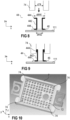
substrate 10 with two holdingpins 44 implemented as sleeves is exemplarily illustrated inFigure 6. Figure 7 schematically illustrates a cross-sectional view of a section of a power semiconductor module arrangement wherein a holdingpin 44 implemented as a sleeve is inserted into arespective holding element 74. As is illustrated inFigures 6 and 7 , and in further detail inFigures 8 and 9 , a holding pin 44 (e.g., a sleeve 442) may comprise at least onecollar 444 arranged at the free end of the holdingpin 44. In the example illustrated inFigures 8 and 9 , the holdingpin 44 comprises twocollars 444, wherein eachcollar 444 is arranged at a different end of the holdingpin 44. As has been described above, a first end of the holdingpin 44 is attached to the substrate 10 (e.g., the first metallization layer 111) by means of asuitable connection layer 46. The holdingpin 44 extends in a vertical direction y perpendicular to thesubstrate 10, and a second (free) end of the holdingpin 44 faces away from thesubstrate 10. An outer diameter d442 of the holding pin 44 (e.g., the sleeve 442) in this example is smaller than the smallest diameter d74 of the holding element 74 (either the inner diameter d742, or the reduced diameter d744). An outer diameter d444 of thecollar 444 is larger than the smallest diameter d74 of the holding element 74 (either the inner diameter d742, or the reduced diameter d744).Figure 8 illustrates the holdingpin 44 and the holdingelement 74 in an unmounted state. - When the holding
pin 44 is inserted into the holdingelement 74, thecollar 444 is bent in a direction towards thesubstrate 10. That is, the holdingpin 44 is pressed into the respective holdingelement 74 with a certain amount of force. After thecollar 444 has been bent, it smoothly adapts to the inner contour of the holdingelement 74. That is, if the holdingelement 74 does not comprise anyribs 744, thecollar 444 is bent along its entire circumference. If, however, the holdingelement 74 comprisesribs 744, thecollar 44 may only be bent in certain sections defined by theribs 744. In other sections, it may remain in its initial form, or may be bent only partly, for example. Deforming thecollar 444 when pressing the holdingpin 44 into the respective holdingelement 74 causes a force-fitting connection to be formed between the holdingpin 44 and the respective holdingelement 74. In this way, a reliable connection between thehousing 7 and thesubstrate 10 is formed which can withstand even comparably high press-out forces (e.g., press-out forces of 30N or even more). - Now referring to
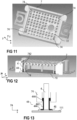
Figure 10 , ahousing 7 for an exemplary powersemiconductor module arrangement 100 is schematically illustrated that comprises four holdingelements 74, wherein each holdingelement 74 is arranged at a different corner of therectangular housing 7. In the example illustrated inFigure 10 , each holdingelement 74 comprises fourribs 744.Figure 11 illustrates a similar arrangement with four holdingelements 74. However, the holdingelements 74 in the example ofFigure 11 do not comprise anyribs 744 at all, similar to what has been described with respect toFigure 5C above. Instead of rectangular, thehousing 7 in these examples can have a square shape instead. - As has been described above, the holding pins 44 are only used to provide a mechanical connection between the
substrate 10 and thehousing 7. When a holdingpin 44 is implemented as asleeve 442, however, it is possible that, in addition to mounting thehousing 7 to thesubstrate 10, the holdingpin 44 is used to accommodate aterminal element 4. A first end of aterminal element 4 may be inserted into the hollow holding pin 44 (sleeve), the holdingpin 44 electrically and mechanically coupling theterminal element 4 to thesubstrate 10. In this example, theconnection layer 46 may be an electricallyconducting connection layer 46. The holdingpin 44 in this example may also comprise an electrically conducting material, for example. A hollow holding pin 44 (sleeve) accommodating aterminal element 4 is exemplarily illustrated in the three-dimensional cross-sectional view ofFigure 12 and in the cross-sectional view ofFigure 13 . The second end of theterminal element 4 may be electrically contacted from outside of thehousing 7, similar to what has been described with respect to theterminal elements 4 inFigure 1 above. - The holding force exerted on the housing 7 (i.e., the holding elements 74) by means of a plurality of holding
pins 44 may not be enough to permanently fix thehousing 7 to thesubstrate 10 during the use of the powersemiconductor module arrangement 100. When exposed to typical stress occurring during the use of the powersemiconductor module arrangement 100, the force applied by the holding pins 44 may not be sufficient to hold thehousing 7 in a desired position with regard to thesubstrate 10. The force, however, is generally sufficient to hold thehousing 7 in a desired position with regard to thesubstrate 10 when shipping the powersemiconductor module arrangement 100 to an end customer. When the powersemiconductor module arrangement 100 is arranged on an additional base plate or heat sink at the customer, which is usually the case, thehousing 7 is usually fixed to the base plate or heat sink permanently by means of additional holding elements, thereby also securing thesubstrate 10 in a desired position with regard to thehousing 7 and the base plate or heat sink. - The arrangement of the holding pins 44 on the
substrate 10 is not restricted to specific positions. One or more holding pins 44 can be arranged in any suitable positions of thesubstrate 10. That is, they can either be arranged close to the edges of thesubstrate 10 or anywhere centrally on thesubstrate 10. The number of holdingpins 44 can be chosen in order to provide sufficient mechanical stability of thehousing 7. According to one example, a powersemiconductor module arrangement 100 comprises between 1 and 4, or between 1 and 8 holding pins 44. Ahousing 7 according to another example that comprises 14 holdingelements 74 is schematically illustrated inFigure 14 . The holdingelements 74 illustrated inFigure 14 are implemented in different ways (different designs). A first holding element 74i, for example, has an oval shape with noribs 744. A second and fourth holdingelement element ribs 744, a fifth holding element 74s has a round shape with threeribs 744, and aseventh holding element 747 has a round shape with noribs 744. Theribs 744 may generally be oriented in any direction. Holdingelements 74 that are oriented in different directions are schematically illustrated at the top ofFigure 14 (holdingelements 74 arranged at the opposite side of the housing 7). Different designs of holdingelements 74 may be combined in onehousing 7, as is illustrated inFigure 14 . It is, however, also possible that onehousing 7 comprises a plurality of holdingelements 74 that all have the same design. It is also possible to combine only two designs, or more than two designs in asingle housing 7. As has been described above, alternatively or additionally to what is illustrated inFigure 14 , any other shape of the holdingelement 74 and/or any other number of holdingelements 744 is also possible. - Less than 14 or even more than 14 holding
elements 74 are generally possible. When thehousing 7 is mounted to thesubstrate 10, not every holdingelement 74 may accommodate arespective holding pin 44. Providing a large number of holdingelements 74 may provide an increased flexibility. Each holdingpin 44 that is arranged on thesubstrate 10 requires a certain amount of space. It is, however, generally desirable to keep the size of asubstrate 10 as small as possible. The number of holdingpins 44 may be chosen according to a minimum number of holdingpins 44 that is required to hold thehousing 7 in its desired position for shipping. This minimum number of holdingpins 44 may depend on a size, material and weight of thesubstrate 10 and thehousing 7, for example. Another important aspect, however, is the exact placement of the different components on thesubstrate 10. For different applications and designs there may be a different amount of space available for the holding pins 44 on thesubstrate 10. The exact placement of the holding pins 44 therefore may also depend on the application and the respective design. Ahousing 7 comprisingmore holding elements 74 than required (more holdingelements 74 than holding pins 44), may be used for many different applications and designs, for example, as the exact placement of the holding pins 44 is not restricted to only few positions on thesubstrate 10. - The holding pins 44 and holding
elements 74 described herein with regard to the different figures can be combined with each other in a single arrangement. That is, a powersemiconductor module arrangement 100 can comprise holdingelements 74 as described with respect toFigure 5A and/or holdingelements 74 as described with respect toFigure 5B , and/or holdingelements 74 as described with respect toFigure 5C . Alternatively or additionally, a powersemiconductor module arrangement 100 may comprise holdingelements 74 that are implemented in any other suitable way. Similarly, one or more holding pins 44 may be implemented as solid pins, and/or one or more holding pins 44 may be implemented as hollow pins, and/or one or more holding pins 44 may be implemented as sleeves, for example. Alternatively or additionally, a powersemiconductor module arrangement 100 may comprise holdingpins 44 that are implemented in any other suitable way.
Claims (14)
- A power semiconductor module arrangement (100) comprising:a housing (7);a substrate (10) forming a ground surface of the housing (7);one or more holding pins (44) mechanically connected to the substrate (10); andone or more holding elements (74) attached to or integrally formed with the housing (7), whereina first end of each of the one or more holding pins (44) is arranged inside the housing (7) and connected to the substrate (10),each of the one or more holding elements (74) comprises a sleeve configured to receive a free end of one of the holding pins (44), andeach of the one or more holding pins (44) extends from the substrate (10) in a vertical direction (y) perpendicular to a top surface of the substrate (10) towards a different one of the one or more holding elements (74) such that the free end (42) of each of the one or more holding pins (44) is arranged inside the respective holding element (74) in order to form a force-fitting connection.
- The power semiconductor module arrangement (100) of claim 1 comprising a single holding element (74) arranged in a central position of a cover of the housing (7).
- The power semiconductor module arrangement (100) of claim 1 comprising two holding elements (74) arranged on opposing sides of the housing (7).
- The power semiconductor module arrangement (100) of claim 1 comprising four holding elements (74), wherein the housing (7) has a rectangular or square cross-section, and each holding element (74) is arranged at a different corner of the housing (7).
- The power semiconductor module arrangement of claim 1 comprising more holding elements (74) than holding pins (44).
- The power semiconductor module arrangement (100) of any of claims 1 to 5, wherein at least one of the one or more the holding elements (74) comprises a sleeve (742) having an inner diameter (d742).
- The power semiconductor module arrangement (100) of claim 6, further comprising a plurality of ribs (744) extending from inner diameter (d742) of the sleeve (742) towards a center of an opening defined by the sleeve (742), the ribs (744) defining a reduced diameter (d744) in defined sections of the sleeve (742), wherein the reduced diameter (d744) is smaller than the inner diameter (d744).
- The power semiconductor module arrangement (100) of claim 6 or 7, whereinat least one of the one or more holding pins (44) comprises a collar (444) arranged at the free end of the respective holding pin (44),an outer diameter (d442) of the holding pin (44) is smaller than a smallest diameter (d74, d742, d744) of the holding element (74), andthe collar (444) is bent in a direction towards the substrate (10) and smoothly adapts to the inner contour of the holding element (74).
- The power semiconductor module arrangement (100) of claim 7, wherein an outer diameter of a holding pin (44) is equal to or larger than the reduced diameter (d744) defined by the ribs (744) and smaller than the inner diameter (d742) of the sleeve (742).
- The power semiconductor module arrangement (100) of any of the preceding claims, whereinat least one of the one or more holding pins (44) comprises a sleeve (442),the power semiconductor module arrangement (100) further comprises at least one terminal element (4), wherein a first end of a different one of the at least one terminal element (4) is arranged in one of the at least one sleeve (442),a second end of the at least one terminal element (4) extends vertically to the outside of the housing (7), andthe respective holding pin (44) electrically and mechanically couples the respective terminal element (4) to the substrate (10).
- The power semiconductor module arrangement of any of the preceding claims, further comprising a connection layer between each of the plurality of holding pins (44) and the substrate (10).
- The power semiconductor module arrangement of claim 11, wherein the connection layer comprises at least one ofa solder layer;an electrically conductive adhesive;an electrically insulating adhesive; anda layer of a sintered metal powder.
- A method for assembling a power semiconductor module arrangement (100), the method comprising:mechanically connecting one or more holding pins (44) to a substrate (10); andarranging a housing (7) on the substrate (10), whereinone or more holding elements (74) are attached to or integrally formed with the housing (7),a first end of each of the one or more holding pins (44) is arranged inside the housing (7) and connected to the substrate (10),each of the one or more holding elements (74) comprises a sleeve configured to receive a free end of one of the one or more holding pins (44), andeach of the one or more holding pins (44) extends from the substrate (10) in a vertical direction (y) perpendicular to a top surface of the substrate (10) towards a different one of the one or more holding elements (74), and arranging the housing (7) on the substrate (10) comprises pressing the free end of each of the one or more holding pins (44) into a different one of the one or more holding elements (74) in order to form a force-fitting connection.
- The method of claim 13, whereinat least one of the one or more holding pins (44) comprises a collar (444) arranged at the free end of the respective holding pin (44),an outer diameter (d442) of the holding pin (44) is smaller than a smallest diameter (d74, d742, d744) of the holding element 74, andwhen pressing the free end of each of the one or more holding pins (44) into one of the holding elements (74), the collar (444) of the respective one of the holding pins (44) is bent in a direction towards the substrate (10).
Priority Applications (3)
| Application Number | Priority Date | Filing Date | Title |
|---|---|---|---|
| EP22205283.9A EP4365935A1 (en) | 2022-11-03 | 2022-11-03 | Power semiconductor module arrangement |
| CN202311458826.8A CN117995830A (en) | 2022-11-03 | 2023-11-02 | Power semiconductor module device |
| US18/386,383 US20240153832A1 (en) | 2022-11-03 | 2023-11-02 | Power Semiconductor Module Arrangement |
Applications Claiming Priority (1)
| Application Number | Priority Date | Filing Date | Title |
|---|---|---|---|
| EP22205283.9A EP4365935A1 (en) | 2022-11-03 | 2022-11-03 | Power semiconductor module arrangement |
Publications (1)
| Publication Number | Publication Date |
|---|---|
| EP4365935A1 true EP4365935A1 (en) | 2024-05-08 |
Family
ID=84330188
Family Applications (1)
| Application Number | Title | Priority Date | Filing Date |
|---|---|---|---|
| EP22205283.9A Pending EP4365935A1 (en) | 2022-11-03 | 2022-11-03 | Power semiconductor module arrangement |
Country Status (3)
| Country | Link |
|---|---|
| US (1) | US20240153832A1 (en) |
| EP (1) | EP4365935A1 (en) |
| CN (1) | CN117995830A (en) |
Citations (2)
| Publication number | Priority date | Publication date | Assignee | Title |
|---|---|---|---|---|
| EP3460837A1 (en) * | 2017-09-26 | 2019-03-27 | Infineon Technologies AG | A housing for a power semiconductor module, a power semiconductor module and a method for producing the same |
| US20200091023A1 (en) * | 2018-09-19 | 2020-03-19 | Infineon Technologies Ag | Power Semiconductor Module Arrangement and Housing for a Power Semiconductor Arrangement |
-
2022
- 2022-11-03 EP EP22205283.9A patent/EP4365935A1/en active Pending
-
2023
- 2023-11-02 US US18/386,383 patent/US20240153832A1/en active Pending
- 2023-11-02 CN CN202311458826.8A patent/CN117995830A/en active Pending
Patent Citations (2)
| Publication number | Priority date | Publication date | Assignee | Title |
|---|---|---|---|---|
| EP3460837A1 (en) * | 2017-09-26 | 2019-03-27 | Infineon Technologies AG | A housing for a power semiconductor module, a power semiconductor module and a method for producing the same |
| US20200091023A1 (en) * | 2018-09-19 | 2020-03-19 | Infineon Technologies Ag | Power Semiconductor Module Arrangement and Housing for a Power Semiconductor Arrangement |
Also Published As
| Publication number | Publication date |
|---|---|
| CN117995830A (en) | 2024-05-07 |
| US20240153832A1 (en) | 2024-05-09 |
Similar Documents
| Publication | Publication Date | Title |
|---|---|---|
| EP3929973B1 (en) | A power semiconductor module and a method for producing a power semiconductor module | |
| US12500152B2 (en) | Power semiconductor module, method for assembling a power semiconductor module and housing for a power semiconductor module | |
| EP3499649B1 (en) | Power semiconductor module arrangement | |
| EP3913665B1 (en) | A power semiconductor module and a method for producing a power semiconductor module | |
| EP3627978B1 (en) | Power semiconductor module arrangement and housing for a power semiconductor arrangement | |
| EP3477694B1 (en) | Power semiconductor module with partially coated power terminals | |
| EP3863045B1 (en) | Power semiconductor module arrangement and method for producing the same | |
| US20240153832A1 (en) | Power Semiconductor Module Arrangement | |
| US11856718B2 (en) | Housing for a power semiconductor module arrangement | |
| EP3736854A1 (en) | Power semiconductor module arrangement | |
| US12456654B2 (en) | Power semiconductor modules | |
| EP4372801A1 (en) | Power semiconductor module arrangement and method for assembling the same | |
| US20250273520A1 (en) | Housing, semiconductor module having a housing, and method for assembling a semiconductor module | |
| CN114975288A (en) | Power semiconductor module device | |
| EP4513531B1 (en) | Housing, semiconductor module comprising a housing, and method for assembling a semiconductor module | |
| EP4270466A1 (en) | Power semiconductor module arrangements and methods for producing power semiconductor module arrangements | |
| US20260094986A1 (en) | Rivet for use in semiconductor module arrangement and method for producing the same | |
| US20260053056A1 (en) | Housing and semiconductor module having a housing | |
| CN120511235A (en) | Semiconductor module arrangement, electronic component carrier for a semiconductor module arrangement and method for producing a semiconductor module arrangement |
Legal Events
| Date | Code | Title | Description |
|---|---|---|---|
| PUAI | Public reference made under article 153(3) epc to a published international application that has entered the european phase |
Free format text: ORIGINAL CODE: 0009012 |
|
| STAA | Information on the status of an ep patent application or granted ep patent |
Free format text: STATUS: REQUEST FOR EXAMINATION WAS MADE |
|
| 17P | Request for examination filed |
Effective date: 20231030 |
|
| AK | Designated contracting states |
Kind code of ref document: A1 Designated state(s): AL AT BE BG CH CY CZ DE DK EE ES FI FR GB GR HR HU IE IS IT LI LT LU LV MC ME MK MT NL NO PL PT RO RS SE SI SK SM TR |