EP4365704A1 - Optical computation device and optical computation method - Google Patents
Optical computation device and optical computation method Download PDFInfo
- Publication number
- EP4365704A1 EP4365704A1 EP21948366.6A EP21948366A EP4365704A1 EP 4365704 A1 EP4365704 A1 EP 4365704A1 EP 21948366 A EP21948366 A EP 21948366A EP 4365704 A1 EP4365704 A1 EP 4365704A1
- Authority
- EP
- European Patent Office
- Prior art keywords
- light
- diffraction element
- light diffraction
- optical computing
- computing device
- Prior art date
- Legal status (The legal status is an assumption and is not a legal conclusion. Google has not performed a legal analysis and makes no representation as to the accuracy of the status listed.)
- Pending
Links
Images



Classifications
-
- G—PHYSICS
- G02—OPTICS
- G02B—OPTICAL ELEMENTS, SYSTEMS OR APPARATUS
- G02B5/00—Optical elements other than lenses
- G02B5/18—Diffraction gratings
-
- G—PHYSICS
- G02—OPTICS
- G02B—OPTICAL ELEMENTS, SYSTEMS OR APPARATUS
- G02B27/00—Optical systems or apparatus not provided for by any of the groups G02B1/00 - G02B26/00, G02B30/00
- G02B27/42—Diffraction optics, i.e. systems including a diffractive element being designed for providing a diffractive effect
- G02B27/4233—Diffraction optics, i.e. systems including a diffractive element being designed for providing a diffractive effect having a diffractive element [DOE] contributing to a non-imaging application
-
- G—PHYSICS
- G02—OPTICS
- G02B—OPTICAL ELEMENTS, SYSTEMS OR APPARATUS
- G02B27/00—Optical systems or apparatus not provided for by any of the groups G02B1/00 - G02B26/00, G02B30/00
- G02B27/42—Diffraction optics, i.e. systems including a diffractive element being designed for providing a diffractive effect
- G02B27/4272—Diffraction optics, i.e. systems including a diffractive element being designed for providing a diffractive effect having plural diffractive elements positioned sequentially along the optical path
-
- G—PHYSICS
- G02—OPTICS
- G02B—OPTICAL ELEMENTS, SYSTEMS OR APPARATUS
- G02B5/00—Optical elements other than lenses
- G02B5/005—Diaphragms
-
- G—PHYSICS
- G02—OPTICS
- G02B—OPTICAL ELEMENTS, SYSTEMS OR APPARATUS
- G02B5/00—Optical elements other than lenses
- G02B5/18—Diffraction gratings
- G02B5/1814—Diffraction gratings structurally combined with one or more further optical elements, e.g. lenses, mirrors, prisms or other diffraction gratings
-
- G—PHYSICS
- G02—OPTICS
- G02B—OPTICAL ELEMENTS, SYSTEMS OR APPARATUS
- G02B5/00—Optical elements other than lenses
- G02B5/18—Diffraction gratings
- G02B5/1866—Transmission gratings characterised by their structure, e.g. step profile, contours of substrate or grooves, pitch variations, materials
- G02B5/1871—Transmissive phase gratings
-
- G—PHYSICS
- G06—COMPUTING OR CALCULATING; COUNTING
- G06E—OPTICAL COMPUTING DEVICES
- G06E3/00—Devices not provided for in group G06E1/00, e.g. for processing analogue or hybrid data
-
- G—PHYSICS
- G06—COMPUTING OR CALCULATING; COUNTING
- G06N—COMPUTING ARRANGEMENTS BASED ON SPECIFIC COMPUTATIONAL MODELS
- G06N3/00—Computing arrangements based on biological models
- G06N3/02—Neural networks
- G06N3/06—Physical realisation, i.e. hardware implementation of neural networks, neurons or parts of neurons
- G06N3/067—Physical realisation, i.e. hardware implementation of neural networks, neurons or parts of neurons using optical means
Definitions
- the present invention relates to an optical computing device and an optical computing method for carrying out optical computing by using a light diffraction element.
- a light diffraction element including multiple cells is known. Such a light diffraction element is designed so that signal light waves that have passed through the cells are caused to interfere with each other to optically carry out predetermined computing. Such optical computing using such a light diffraction element has the advantages of high speed computing and low power consumption, as compared with electrical computing using a processor. Furthermore, it is possible to achieve multi-step optical computing (optical computing with two or more steps) by, in turn, causing two or more light diffraction elements arranged in a row to work on signal light.
- Patent Literature 1 discloses an optical neural network having an input layer, an intermediate layer, and an output layer.
- the abovementioned light diffraction element can be utilized as, for example, an intermediate layer for such an optical neural network.
- Patent Literature 1 Specification of US Patent No. 7847225
- a conventional optical computing device light emitted from a display that displays an image including an object as a photographic subject is input into a light diffraction element group, to have the light undergo optical computing of visual information of the object.
- a light diffraction element group to have the light undergo optical computing of visual information of the object.
- An aspect of the present invention has been made in view of such circumstances, and an object of the aspect is to provide an optical computing device or an optical computing method that are capable of carrying out optical computing at a high speed with a high degree of efficiency.
- an optical computing device in accordance with an aspect of the present invention is an optical computing device including a light diffraction element group including at least one light diffraction element having an optical computing function, wherein the light diffraction element group is arranged so as to allow light to pass through the at least one light diffraction element included in the light diffraction element group in turn, the light being light having been reflected or scattered from an object that is located outside the optical computing device, is other than a display, and is not an illuminant, or light having been emitted from an object that is located outside the optical computing device, is other than the display, and is an illuminant.
- an optical computing method in accordance with an aspect of the present invention is an optical computing method for carrying out optical computing by using an optical computing device including a light diffraction element group including at least one light diffraction element, including the step of allowing light to pass through the at least one light diffraction element included in the light diffraction element group in turn, the light being light having been reflected or scattered from an object that is located outside the optical computing device, is other than a display, and is not an illuminant, or light having been emitted from an object that is located outside the optical computing device, is other than the display, and is an illuminant.
- an optical computing device or an optical computing method that are capable of carrying out optical computing at a high speed with a high degree of efficiency.
- FIG. 1 A configuration of an optical computing device 1 in accordance with an embodiment of the present invention will be described with reference to Fig. 1.
- (a) of Fig. 1 is a perspective view of the optical computing device 1
- (b) of Fig. 1 is a plan view of the optical computing device 1.
- the optical computing device 1 includes a light diffraction element group 11 and a filter 12, as illustrated in Fig. 1 .
- the light diffraction element group 11 is a set of n light diffraction elements 11a1 to 11a n .
- n is any natural number of 1 or more.
- Each light diffraction element 11a i is an element that has an optical computing function, which is a function for converting a two-dimensional intensity distribution of signal light in accordance with a predetermined conversion rule.
- i is a natural number of 1 or more and n or less.
- Fig. 1 illustrates a set of three light diffraction elements 11a1 to 11a3 as the light diffraction element group 11. A specific example of each light diffraction element 11a i will be described later with reference to Fig. 3 .
- the light diffraction element group 11 is provided so that a first light diffraction element 11a1, a second light diffraction element 11a2, ..., and an n th light diffraction element 11a n are arranged in a straight line on an optical path of signal light.
- signal light input into the light diffraction element group 11 passes through the first light diffraction element 11a1, the second light diffraction element 11a2, ..., and the n th light diffraction element 11a n in this order.
- the signal light is subjected to first optical computing carried out by the first light diffraction element 11a1, second optical computing carried out by the second light diffraction element 11a2, ..., and n th optical computing carried out by the n th light diffraction element 11a n , in this order.
- the two-dimensional intensity distribution of signal light output from the light diffraction element group 11 indicates computation results of these computing processes.
- the filter 12 is located at a stage that precedes the light diffraction element group 11.
- the filter 12 is configured to selectively guide, to the light diffraction element group 11, light which travels in a direction that forms an angle ⁇ of less than or equal to a specific angle with an optical axis L1 of the first light diffraction element 11a1 on which signal light is incident first.
- a diaphragm having an aperture 12a is used as the filter 12.
- the specific angle is a maximum value ⁇ 1 of the angle formed between the optical axis L1 and an optical axis of a light beam that has passed through the aperture 12a of the filter 12, which is a diaphragm, and that is incident on the first light diffraction element 11a1.
- a light wave having an angle ⁇ that is formed between the travel direction thereof and the optical axis L1 and that is greater than the specific angle ⁇ 1 is absorbed by the filter 12.
- a conventional optical computing device In a conventional optical computing device, light emitted from a display that displays an image including an object S as a photographic subject is input into a light diffraction element group, to have the light undergo optical computing of visual information of the object S.
- light from the object S itself is input into the light diffraction element group 11, to have the light undergo optical computing of visual information of the object S.
- the light diffraction element group 11 is arranged so as to allow the light from the object S itself to pass through in turn the n light diffraction elements 11a1 to 11a included in the light diffraction element group 11.
- the "object S” refers to a physical object that is located outside the optical computing device 11 and is other than a display.
- the wording "light from the object S itself” refers to light having been reflected or scattered from the object S in a case in which the object S is not an illuminant, whereas it refers to light having been emitted from the object S in a case in which the object S is an illuminant.
- the optical computing device 1 may further include an additional image sensor that converts, to an electrical signal, the signal light output from the light diffraction element group 11.
- Examples of the additional image sensor may include a two-dimensional image sensor that includes multiple light receiving cells arranged in a matrix pattern.
- FIG. 2 are plan views each illustrating the filter 12 and the first light diffraction element 11a1 of the optical computing device 1.
- Light from point Pa that is close to the optical axis L1 of the first light diffraction element 11a1 forms an angle ⁇ of less than or equal to the abovementioned specific angle ⁇ 1 between the travel direction and the optical axis L1, as illustrated in (a) of Fig. 2 , and thus, the light can pass through the aperture 12a and be incident on the first light diffraction element 11a1.
- One possible example of such light may be light from the object S, that is, signal light.
- light from point Pb that is far from the optical axis L1 of the first light diffraction element 11a1 forms an angle ⁇ of greater than the abovementioned specific angle ⁇ 1 between the travel direction and the optical axis L1, as illustrated in (b) of Fig. 2 , and thus, the light cannot pass through the aperture 12a and cannot be incident on the first light diffraction element 11a1.
- One possible example of such light may be light other than light from the object S, that is, noise light.
- use of the filter 12 makes it possible to prevent noise light from being incident on the first light diffraction element 11a1, without preventing signal light from being incident on the first light diffraction element 11a1. Therefore, it is possible to prevent a decrease in computation accuracy due to noise light.
- FIG. 3 is a plan view of the light diffraction element 11a i in accordance with the present specific example.
- (b) of Fig. 3 is a partial enlarged perspective view of the light diffraction element 11a i in accordance with the present specific example (illustrating a portion indicated by the dotted line in (a) of Fig. 3 ).
- the light diffraction element 11a i is constituted by multiple microcells with thicknesses and refractive indexes set independently of each other.
- the resulting signal light waves diffracted by the microcells and having different phases interfere with each other.
- This achieves a predetermined optical computing (conversion of two-dimensional intensity distribution in accordance with a predetermined conversion rule).
- the "microcell” refers to a cell that may have a cell size of less than 10 pm, for example.
- the "cell size” refers to a square root of an area of a cell. For example, when a microcell has a square shape in a plan view, the cell size corresponds to the length of a side of the cell. A lower limit of the cell size may be, for example, 1 nm.
- the light diffraction element 11a i illustrated in Fig. 3 is constituted by 200 x 200 microcells arranged in a matrix pattern. Each microcell has a square shape with a size of 500 nm x 500 nm in a plan view, and the light diffraction element 11a i has a square shape with a size of 100 pm x 100 pm in a plan view.
- a phase shift amount of signal light passing through microcells can be independently set for each cell by (1) a method in which a thickness of a microcell is independently set for each cell, or (2) a method in which a refractive index of a microcell is independently set for each cell.
- the method (1) which can be carried out by nanoimprinting, is employed.
- each microcell is constituted by a quadrangular prism-shaped pillar having a square bottom surface with four sides that are all equal to the cell size, as illustrated in (b) of Fig. 3 .
- the phase shift amount of signal light transmitted through each microcell varies depending on the height of the pillar constituting the corresponding microcell. That is, as the height of the pillar constituting the microcell increases, the phase shift amount of signal light transmitted through the microcell increases, and as the height of the pillar constituting the microcell decreases, the phase shift amount of signal light transmitted through the microcell decreases.
- the thickness or refractive index of each microcell may be set by, for example, machine learning.
- a model used in this machine learning may be, for example, a model into which a two-dimensional intensity distribution of signal light input into the light diffraction element 11a i is input, and from which a two-dimensional intensity distribution of signal light output from the light diffraction element 11a i is output, and in which thicknesses or refractive indexes of the microcells are included as parameters.
- the "two-dimensional intensity distribution of signal light input into the light diffraction element 11a i " refers to a set of intensities of signal light waves input into microcells which constitute the light diffraction element 11a i .
- the "two-dimensional intensity distribution of signal light output from the light diffraction element 11a i " refers to a set of intensities of signal light waves each input into a microcell constituting light diffraction element 11a i +1, located at a stage that follows the light diffraction element 11a i , or a set of intensities of signal light waves input into cells which constitute a light receiving unit that is located at the stage that follows the light diffraction element 11a i .
- optical computing device 1A A first modification of the optical computing device 1 (hereinafter, referred to as "optical computing device 1A") will be described with reference to Fig. 4.
- (a) of Fig. 4 is a perspective view of the optical computing device 1A
- (b) of Fig. 4 is a plan view of the optical computing device 1A.
- a difference between the optical computing device 1A and the optical computing device 1 is that the optical computing device 1 uses a diaphragm as the filter 12, whereas the optical computing device 1A uses a block as a filter 12A.
- the block is constituted by a material having a refractive index greater than that of air and is disposed so that a surface 12A1 of the block on a side opposite to a side facing the first light diffraction element 11a1 is orthogonal to the optical axis L1.
- the filter 12A selectively guides, to the light diffraction element group 11, light which travels in a direction that forms an angle ⁇ of less than or equal to a specific angle with the optical axis L1 of the first light diffraction element 11a1.
- the specific angle is a critical angle ⁇ 2 at the surface 12A1 of the block constituting the filter 12A.
- a light wave having an angle ⁇ that is formed between the travel direction thereof and the optical axis L1 and that is greater than the specific angle ⁇ 2 is totally reflected by the filter 12A.
- FIG. 5 are plan views each illustrating the filter 12A and the first light diffraction element 11a1 of the optical computing device 1A.
- Light from point Pa that is close to the optical axis L1 of the first light diffraction element 11a1 forms an angle ⁇ of less than or equal to the abovementioned specific angle ⁇ 2 between the travel direction and the optical axis L1, as illustrated in (a) of Fig. 5 , and thus, the light can be incident on the first light diffraction element 11a1.
- One possible example of such light may be light from the object S, that is, signal light.
- light from point Pb that is far from the optical axis L1 of the first light diffraction element 11a1 forms an angle ⁇ of greater than the abovementioned specific angle ⁇ 2 between the travel direction and the optical axis L1, as illustrated in (b) of Fig. 5 , and thus, the light cannot be incident on the first light diffraction element 11a1.
- One possible example of such light may be light other than light from the object S, that is, noise light.
- the optical computing device 1A it is possible to prevent noise light from being incident on the first light diffraction element 11a1, without preventing signal light from being incident on the first light diffraction element 11a1. Therefore, it is possible to prevent a decrease in computation accuracy due to noise light.
- optical computing device 1B A first modification of the optical computing device 2 (hereinafter, referred to as "optical computing device 1B") will be described with reference to Fig. 6.
- (a) of Fig. 6 is a perspective view of the optical computing device 1B
- (b) of Fig. 6 is a plan view of the optical computing device 1B.
- a difference between the optical computing device 1B and the optical computing device 1 is that the optical computing device 1 uses a diaphragm as the filter 12, whereas the optical computing device 1B uses a lens as a filter 12B.
- the lens is constituted by a material having a refractive index greater than that of air, and is disposed so that the optical axis of this lens coincides with the optical axis of the first light diffraction element 11a1.
- the filter 12B selectively guides, to the light diffraction element group 11, light which travels in a direction that forms an angle ⁇ of less than or equal to a specific angle with the optical axis L1 of the first light diffraction element 11a1.
- the specific angle is a maximum value ⁇ 3 of the angle formed between the optical axis L1 and an optical axis of a light beam before incidence on the filter 12B, which is a lens, the light beam traveling in a direction that allows the light beam to pass through the filter 12B, which is a lens, and to be incident on the first light diffraction element 11a1.
- FIG. 7 are plan views each illustrating the filter 12B and the first light diffraction element 11a1 of the optical computing device 1B.
- Light from point Pa that is close to the optical axis L1 of the first light diffraction element 11a1 forms an angle ⁇ of less than or equal to the abovementioned specific angle ⁇ 3 between the travel direction and the optical axis L1, as illustrated in (a) of Fig. 7 , and thus, the light can be incident on the first light diffraction element 11a1.
- One possible example of such light may be light from the object S, that is, signal light.
- light from point Pb that is far from the optical axis L1 of the first light diffraction element 11a1 forms an angle ⁇ of greater than the abovementioned specific angle ⁇ 3 between the travel direction and the optical axis L1, as illustrated in (b) of Fig. 7 , and thus, the light cannot be incident on the first light diffraction element 11a1.
- One possible example of such light may be light other than light from the object S, that is, noise light.
- the optical computing device 1B it is possible to prevent noise light from being incident on the first light diffraction element 11a1, without preventing signal light from being incident on the first light diffraction element 11a1. Therefore, it is possible to prevent a decrease in computation accuracy due to noise light.
- FIG. 8 is a perspective view of the optical computing device 1C.
- the light source 13 is configured to emit light for illuminating the object S, to a limited specific area including the optical axis L1 of the first light diffraction element 11a1.
- the object S is a sheet of paper on which some numerals are depicted, and the light diffraction element group 11 is designed to determine which numeral from 0 to 9 is depicted on the sheet of paper.
- an area to be illuminated by the light source 13 is not limited, what might be incident on the light diffraction element group 11 is not only light (signal light) having been reflected or scattered at a region of interest in the object S (in the illustrated example, a region in which "4" is depicted), but also light (noise light) having been reflected or scattered at a region other than the region of interest in the object S (in the illustrated example, regions in which "3" and "5" are depicted) or having been reflected or scattered from a physical object other than the object S.
- an area to be illuminated by the light source 13 is limited to a specific area including the optical axis L1 of the first light diffraction element 11a1, only light having been reflected or scattered at a region of interest in the object S (in the illustrated example, the region in which "4" is depicted) is incident on the light diffraction element group 11.
- the optical computing device 1C it is possible to prevent noise light from being incident on the first light diffraction element 11a1, without preventing signal light from being incident on the first light diffraction element 11a1. Therefore, it is possible to prevent a decrease in computation accuracy due to noise light.
- An optical computing device including a light diffraction element group including at least one light diffraction element having an optical computing function, wherein the light diffraction element group is arranged so as to allow light to pass through the at least one light diffraction element included in the light diffraction element group in turn, the light being light having been reflected or scattered from an object that is located outside the optical computing device, is other than a display, and is not an illuminant, or light having been emitted from an object that is located outside the optical computing device, is other than the display, and is an illuminant.
- the optical computing device further including a filter located at a stage that precedes the light diffraction element group, wherein the filter selectively transmits light which travels in a direction that forms an angle of less than or equal to a specific angle with an optical axis of a first light diffraction element on which signal light is incident first among the at least one light diffraction element included in the light diffraction element group.
- the filter is a diaphragm
- the specific angle is a maximum value of the angle formed between the optical axis of the first light diffraction element and a light beam that has passed through an aperture of the diaphragm and is incident on the first light diffraction element.
- the optical computing device further including a light source that emits light for illuminating the object, to a limited specific area including an optical axis of the first light diffraction element.
- the light diffraction element group includes at least one light diffraction element including multiple microcells with thicknesses and refractive indexes set independently of each other.
- An optical computing method for carrying out optical computing by using an optical computing device including a light diffraction element group including at least one light diffraction element including the step of allowing light to pass through at least one light diffraction element included in the light diffraction element group in turn, the light being light having been reflected or scattered from an object that is located outside the optical computing device, is other than a display, and is not an illuminant, or light having been emitted from an object that is located outside the optical computing device, is other than the display, and is an illuminant.
- the present invention is not limited to the foregoing embodiments, but can be modified by a person skilled in the art within the scope of the claims.
- the present invention also encompasses, in its technical scope, any embodiment derived by combining technical means disclosed in the foregoing embodiments.
Landscapes
- Physics & Mathematics (AREA)
- General Physics & Mathematics (AREA)
- Optics & Photonics (AREA)
- Engineering & Computer Science (AREA)
- Theoretical Computer Science (AREA)
- Health & Medical Sciences (AREA)
- Life Sciences & Earth Sciences (AREA)
- Biomedical Technology (AREA)
- Biophysics (AREA)
- Artificial Intelligence (AREA)
- Neurology (AREA)
- Computational Linguistics (AREA)
- Data Mining & Analysis (AREA)
- Evolutionary Computation (AREA)
- General Health & Medical Sciences (AREA)
- Molecular Biology (AREA)
- Computing Systems (AREA)
- General Engineering & Computer Science (AREA)
- Mathematical Physics (AREA)
- Software Systems (AREA)
- Diffracting Gratings Or Hologram Optical Elements (AREA)
Abstract
Description
- The present invention relates to an optical computing device and an optical computing method for carrying out optical computing by using a light diffraction element.
- A light diffraction element including multiple cells is known. Such a light diffraction element is designed so that signal light waves that have passed through the cells are caused to interfere with each other to optically carry out predetermined computing. Such optical computing using such a light diffraction element has the advantages of high speed computing and low power consumption, as compared with electrical computing using a processor. Furthermore, it is possible to achieve multi-step optical computing (optical computing with two or more steps) by, in turn, causing two or more light diffraction elements arranged in a row to work on signal light.
-
Patent Literature 1 discloses an optical neural network having an input layer, an intermediate layer, and an output layer. The abovementioned light diffraction element can be utilized as, for example, an intermediate layer for such an optical neural network. - [Patent Literature 1]
Specification ofUS Patent No. 7847225 - However, in a conventional optical computing device, light emitted from a display that displays an image including an object as a photographic subject is input into a light diffraction element group, to have the light undergo optical computing of visual information of the object. Thus, in order to generate an image including the object as a photographic subject, it is necessary to convert an optical signal to an electrical signal by using an image sensor. In addition, in order to display the image including the object as a photographic subject, it is necessary to convert the electrical signal to an optical signal by using a display. Therefore, such a conventional optical computing device has room for improvement in both speed and efficiency.
- An aspect of the present invention has been made in view of such circumstances, and an object of the aspect is to provide an optical computing device or an optical computing method that are capable of carrying out optical computing at a high speed with a high degree of efficiency.
- To achieve the object, an optical computing device in accordance with an aspect of the present invention is an optical computing device including a light diffraction element group including at least one light diffraction element having an optical computing function, wherein the light diffraction element group is arranged so as to allow light to pass through the at least one light diffraction element included in the light diffraction element group in turn, the light being light having been reflected or scattered from an object that is located outside the optical computing device, is other than a display, and is not an illuminant, or light having been emitted from an object that is located outside the optical computing device, is other than the display, and is an illuminant.
- To achieve the object, an optical computing method in accordance with an aspect of the present invention is an optical computing method for carrying out optical computing by using an optical computing device including a light diffraction element group including at least one light diffraction element, including the step of allowing light to pass through the at least one light diffraction element included in the light diffraction element group in turn, the light being light having been reflected or scattered from an object that is located outside the optical computing device, is other than a display, and is not an illuminant, or light having been emitted from an object that is located outside the optical computing device, is other than the display, and is an illuminant.
- According to the aspects of the present invention, it is possible to provide an optical computing device or an optical computing method that are capable of carrying out optical computing at a high speed with a high degree of efficiency.
-
- (a) of
Fig. 1 is a perspective view of an optical computing device in accordance with an embodiment of the present invention. (b) ofFig. 1 is a plan view of the optical computing device. - (a) and (b) of
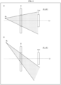
Fig. 2 are plan views each illustrating a first light diffraction element and a filter (diaphragm) that are provided in the optical computing device illustrated inFig. 1. (a) ofFig. 2 illustrates behavior of light (signal light) from a point that is close to an optical axis of the first light diffraction element, and (b) ofFig. 2 illustrates behavior of light (noise light) from a point that is far from the optical axis of the first light diffraction element. - (a) of
Fig. 3 is a plan view of a light diffraction element provided in the optical computing device illustrated inFig. 1. (b) ofFig. 3 is a partial enlarged perspective view of the light diffraction element. - (a) of
Fig. 4 is a perspective view of an optical computing device in accordance with a first modification of the optical computing device illustrated inFig. 1. (b) ofFig. 4 is a plan view of the optical computing device. - (a) and (b) of
Fig. 5 are plan views each illustrating a first light diffraction element and a filter (block) that are provided in the optical computing device illustrated inFig. 4. (a) ofFig. 5 illustrates behavior of light (signal light) from a point that is close to an optical axis of the first light diffraction element, and (b) ofFig. 5 illustrates behavior of light (noise light) from a point that is far from the optical axis of the first light diffraction element. - (a) of
Fig. 6 is a perspective view of an optical computing device in accordance with a second modification of the optical computing device illustrated inFig. 1. (b) ofFig. 6 is a plan view of the optical computing device. - (a) and (b) of
Fig. 7 are plan views each illustrating a first light diffraction element and a filter (lens) that are provided in the optical computing device illustrated inFig. 6. (a) ofFig. 7 illustrates behavior of light (signal light) from a point that is close to an optical axis of the first light diffraction element, and (b) ofFig. 7 illustrates behavior of light (noise light) from a point that is far from the optical axis of the first light diffraction element. -
Fig. 8 is a perspective view of an optical computing device in accordance with a third modification of the optical computing device illustrated inFig. 1 . - A configuration of an
optical computing device 1 in accordance with an embodiment of the present invention will be described with reference toFig. 1. (a) ofFig. 1 is a perspective view of theoptical computing device 1, and (b) ofFig. 1 is a plan view of theoptical computing device 1. - The
optical computing device 1 includes a lightdiffraction element group 11 and afilter 12, as illustrated inFig. 1 . - The light
diffraction element group 11 is a set of n light diffraction elements 11a1 to 11an. Here, n is any natural number of 1 or more. Each light diffraction element 11ai is an element that has an optical computing function, which is a function for converting a two-dimensional intensity distribution of signal light in accordance with a predetermined conversion rule. Here, i is a natural number of 1 or more and n or less.Fig. 1 illustrates a set of three light diffraction elements 11a1 to 11a3 as the lightdiffraction element group 11. A specific example of each light diffraction element 11ai will be described later with reference toFig. 3 . - The light
diffraction element group 11 is provided so that a first light diffraction element 11a1, a second light diffraction element 11a2, ..., and an nth light diffraction element 11an are arranged in a straight line on an optical path of signal light. Thus, signal light input into the lightdiffraction element group 11 passes through the first light diffraction element 11a1, the second light diffraction element 11a2, ..., and the nth light diffraction element 11an in this order. Therefore, in the lightdiffraction element group 11, the signal light is subjected to first optical computing carried out by the first light diffraction element 11a1, second optical computing carried out by the second light diffraction element 11a2, ..., and nth optical computing carried out by the nth light diffraction element 11an, in this order. The two-dimensional intensity distribution of signal light output from the lightdiffraction element group 11 indicates computation results of these computing processes. - The
filter 12 is located at a stage that precedes the lightdiffraction element group 11. Thefilter 12 is configured to selectively guide, to the lightdiffraction element group 11, light which travels in a direction that forms an angle θ of less than or equal to a specific angle with an optical axis L1 of the first light diffraction element 11a1 on which signal light is incident first. According to the present embodiment, a diaphragm having anaperture 12a is used as thefilter 12. Thus, the specific angle is a maximum value θ1 of the angle formed between the optical axis L1 and an optical axis of a light beam that has passed through theaperture 12a of thefilter 12, which is a diaphragm, and that is incident on the first light diffraction element 11a1. Among light waves that have been incident on thefilter 12, a light wave having an angle θ that is formed between the travel direction thereof and the optical axis L1 and that is greater than the specific angle θ1, is absorbed by thefilter 12. - In a conventional optical computing device, light emitted from a display that displays an image including an object S as a photographic subject is input into a light diffraction element group, to have the light undergo optical computing of visual information of the object S. In contrast, in the
optical computing device 1 in accordance with the present embodiment, light from the object S itself is input into the lightdiffraction element group 11, to have the light undergo optical computing of visual information of the object S. To achieve this, the lightdiffraction element group 11 is arranged so as to allow the light from the object S itself to pass through in turn the n light diffraction elements 11a1 to 11a included in the lightdiffraction element group 11. Herein, the "object S" refers to a physical object that is located outside theoptical computing device 11 and is other than a display. The wording "light from the object S itself" refers to light having been reflected or scattered from the object S in a case in which the object S is not an illuminant, whereas it refers to light having been emitted from the object S in a case in which the object S is an illuminant. With this, there is no need, in theoptical computing device 1 in accordance with the present embodiment, to convert an optical signal to an electrical signal to generate an image including the object S as a photographic subject. In addition, there is no need to convert an electrical signal to an optical signal to display the image including the object S as a photographic subject. Thus, according to theoptical computing device 1 in accordance with the present embodiment, it is possible to carry out high-speed and efficient optical computing of visual information of the object S, compared with a conventional optical computing device. - The
optical computing device 1 may further include an additional image sensor that converts, to an electrical signal, the signal light output from the lightdiffraction element group 11. Examples of the additional image sensor may include a two-dimensional image sensor that includes multiple light receiving cells arranged in a matrix pattern. - Effects achieved by the
filter 12 of theoptical computing device 1 will be described with reference toFig. 2. (a) and (b) ofFig. 2 are plan views each illustrating thefilter 12 and the first light diffraction element 11a1 of theoptical computing device 1. - Light from point Pa that is close to the optical axis L1 of the first light diffraction element 11a1 forms an angle θ of less than or equal to the abovementioned specific angle θ1 between the travel direction and the optical axis L1, as illustrated in (a) of
Fig. 2 , and thus, the light can pass through theaperture 12a and be incident on the first light diffraction element 11a1. One possible example of such light may be light from the object S, that is, signal light. - On the other hand, light from point Pb that is far from the optical axis L1 of the first light diffraction element 11a1 forms an angle θ of greater than the abovementioned specific angle θ1 between the travel direction and the optical axis L1, as illustrated in (b) of
Fig. 2 , and thus, the light cannot pass through theaperture 12a and cannot be incident on the first light diffraction element 11a1. One possible example of such light may be light other than light from the object S, that is, noise light. - Thus, use of the
filter 12 makes it possible to prevent noise light from being incident on the first light diffraction element 11a1, without preventing signal light from being incident on the first light diffraction element 11a1. Therefore, it is possible to prevent a decrease in computation accuracy due to noise light. - The following description will describe a specific example of the light diffraction element 11ai with reference to
Fig. 3. (a) ofFig. 3 is a plan view of the light diffraction element 11ai in accordance with the present specific example. (b) ofFig. 3 is a partial enlarged perspective view of the light diffraction element 11ai in accordance with the present specific example (illustrating a portion indicated by the dotted line in (a) ofFig. 3 ). - The light diffraction element 11ai is constituted by multiple microcells with thicknesses and refractive indexes set independently of each other. When signal light is incident on the light diffraction element 11ai, the resulting signal light waves diffracted by the microcells and having different phases interfere with each other. This achieves a predetermined optical computing (conversion of two-dimensional intensity distribution in accordance with a predetermined conversion rule). As used herein, the "microcell" refers to a cell that may have a cell size of less than 10 pm, for example. As used herein, the "cell size" refers to a square root of an area of a cell. For example, when a microcell has a square shape in a plan view, the cell size corresponds to the length of a side of the cell. A lower limit of the cell size may be, for example, 1 nm.
- The light diffraction element 11ai illustrated in
Fig. 3 is constituted by 200 x 200 microcells arranged in a matrix pattern. Each microcell has a square shape with a size of 500 nm x 500 nm in a plan view, and the light diffraction element 11ai has a square shape with a size of 100 pm x 100 pm in a plan view. - A phase shift amount of signal light passing through microcells can be independently set for each cell by (1) a method in which a thickness of a microcell is independently set for each cell, or (2) a method in which a refractive index of a microcell is independently set for each cell. In the present embodiment, the method (1), which can be carried out by nanoimprinting, is employed. In this case, each microcell is constituted by a quadrangular prism-shaped pillar having a square bottom surface with four sides that are all equal to the cell size, as illustrated in (b) of
Fig. 3 . Furthermore, in this case, the phase shift amount of signal light transmitted through each microcell varies depending on the height of the pillar constituting the corresponding microcell. That is, as the height of the pillar constituting the microcell increases, the phase shift amount of signal light transmitted through the microcell increases, and as the height of the pillar constituting the microcell decreases, the phase shift amount of signal light transmitted through the microcell decreases. - Note that the thickness or refractive index of each microcell may be set by, for example, machine learning. A model used in this machine learning may be, for example, a model into which a two-dimensional intensity distribution of signal light input into the light diffraction element 11ai is input, and from which a two-dimensional intensity distribution of signal light output from the light diffraction element 11ai is output, and in which thicknesses or refractive indexes of the microcells are included as parameters. Here, the "two-dimensional intensity distribution of signal light input into the light diffraction element 11ai" refers to a set of intensities of signal light waves input into microcells which constitute the light diffraction element 11ai. Further, the "two-dimensional intensity distribution of signal light output from the light diffraction element 11ai" refers to a set of intensities of signal light waves each input into a microcell constituting light diffraction
element 11ai+ 1, located at a stage that follows the light diffraction element 11ai, or a set of intensities of signal light waves input into cells which constitute a light receiving unit that is located at the stage that follows the light diffraction element 11ai. - A first modification of the optical computing device 1 (hereinafter, referred to as "
optical computing device 1A") will be described with reference toFig. 4. (a) ofFig. 4 is a perspective view of theoptical computing device 1A, and (b) ofFig. 4 is a plan view of theoptical computing device 1A. - A difference between the
optical computing device 1A and theoptical computing device 1 is that theoptical computing device 1 uses a diaphragm as thefilter 12, whereas theoptical computing device 1A uses a block as afilter 12A. The block is constituted by a material having a refractive index greater than that of air and is disposed so that a surface 12A1 of the block on a side opposite to a side facing the first light diffraction element 11a1 is orthogonal to the optical axis L1. - Similarly to the
filter 12, thefilter 12A selectively guides, to the lightdiffraction element group 11, light which travels in a direction that forms an angle θ of less than or equal to a specific angle with the optical axis L1 of the first light diffraction element 11a1. In the present modification, the specific angle is a critical angle Θ2 at the surface 12A1 of the block constituting thefilter 12A. Among light waves that have been incident on thefilter 12A, a light wave having an angle θ that is formed between the travel direction thereof and the optical axis L1 and that is greater than the specific angle Θ2, is totally reflected by thefilter 12A. - Effects achieved by the
optical computing device 1A will be described with reference toFig. 5. (a) and (b) ofFig. 5 are plan views each illustrating thefilter 12A and the first light diffraction element 11a1 of theoptical computing device 1A. - Light from point Pa that is close to the optical axis L1 of the first light diffraction element 11a1 forms an angle θ of less than or equal to the abovementioned specific angle Θ2 between the travel direction and the optical axis L1, as illustrated in (a) of
Fig. 5 , and thus, the light can be incident on the first light diffraction element 11a1. One possible example of such light may be light from the object S, that is, signal light. - On the other hand, light from point Pb that is far from the optical axis L1 of the first light diffraction element 11a1 forms an angle θ of greater than the abovementioned specific angle Θ2 between the travel direction and the optical axis L1, as illustrated in (b) of
Fig. 5 , and thus, the light cannot be incident on the first light diffraction element 11a1. One possible example of such light may be light other than light from the object S, that is, noise light. - Thus, according to the
optical computing device 1A, it is possible to prevent noise light from being incident on the first light diffraction element 11a1, without preventing signal light from being incident on the first light diffraction element 11a1. Therefore, it is possible to prevent a decrease in computation accuracy due to noise light. - A first modification of the optical computing device 2 (hereinafter, referred to as "
optical computing device 1B") will be described with reference toFig. 6. (a) ofFig. 6 is a perspective view of theoptical computing device 1B, and (b) ofFig. 6 is a plan view of theoptical computing device 1B. - A difference between the
optical computing device 1B and theoptical computing device 1 is that theoptical computing device 1 uses a diaphragm as thefilter 12, whereas theoptical computing device 1B uses a lens as afilter 12B. The lens is constituted by a material having a refractive index greater than that of air, and is disposed so that the optical axis of this lens coincides with the optical axis of the first light diffraction element 11a1. - Similarly to the
filter 12, thefilter 12B selectively guides, to the lightdiffraction element group 11, light which travels in a direction that forms an angle θ of less than or equal to a specific angle with the optical axis L1 of the first light diffraction element 11a1. In the present modification, the specific angle is a maximum value θ3 of the angle formed between the optical axis L1 and an optical axis of a light beam before incidence on thefilter 12B, which is a lens, the light beam traveling in a direction that allows the light beam to pass through thefilter 12B, which is a lens, and to be incident on the first light diffraction element 11a1. - Effects achieved by the
optical computing device 1B will be described with reference toFig. 7. (a) and (b) ofFig. 7 are plan views each illustrating thefilter 12B and the first light diffraction element 11a1 of theoptical computing device 1B. - Light from point Pa that is close to the optical axis L1 of the first light diffraction element 11a1 forms an angle θ of less than or equal to the abovementioned specific angle θ3 between the travel direction and the optical axis L1, as illustrated in (a) of
Fig. 7 , and thus, the light can be incident on the first light diffraction element 11a1. One possible example of such light may be light from the object S, that is, signal light. - On the other hand, light from point Pb that is far from the optical axis L1 of the first light diffraction element 11a1 forms an angle θ of greater than the abovementioned specific angle θ3 between the travel direction and the optical axis L1, as illustrated in (b) of
Fig. 7 , and thus, the light cannot be incident on the first light diffraction element 11a1. One possible example of such light may be light other than light from the object S, that is, noise light. - Thus, according to the
optical computing device 1B, it is possible to prevent noise light from being incident on the first light diffraction element 11a1, without preventing signal light from being incident on the first light diffraction element 11a1. Therefore, it is possible to prevent a decrease in computation accuracy due to noise light. - A first modification of the optical computing device 1 (hereinafter, referred to as "optical computing device 1C") will be described with reference to
Fig. 8. Fig. 8 is a perspective view of the optical computing device 1C. - Differences between the optical computing device 1C and the
optical computing device 1 are that thefilter 12 is omitted and alight source 13 is added in the optical computing device 1C. Thelight source 13 is configured to emit light for illuminating the object S, to a limited specific area including the optical axis L1 of the first light diffraction element 11a1. In the illustrated configuration, the object S is a sheet of paper on which some numerals are depicted, and the lightdiffraction element group 11 is designed to determine which numeral from 0 to 9 is depicted on the sheet of paper. - If an area to be illuminated by the
light source 13 is not limited, what might be incident on the lightdiffraction element group 11 is not only light (signal light) having been reflected or scattered at a region of interest in the object S (in the illustrated example, a region in which "4" is depicted), but also light (noise light) having been reflected or scattered at a region other than the region of interest in the object S (in the illustrated example, regions in which "3" and "5" are depicted) or having been reflected or scattered from a physical object other than the object S. In contrast, if an area to be illuminated by thelight source 13 is limited to a specific area including the optical axis L1 of the first light diffraction element 11a1, only light having been reflected or scattered at a region of interest in the object S (in the illustrated example, the region in which "4" is depicted) is incident on the lightdiffraction element group 11. - Thus, according to the optical computing device 1C, it is possible to prevent noise light from being incident on the first light diffraction element 11a1, without preventing signal light from being incident on the first light diffraction element 11a1. Therefore, it is possible to prevent a decrease in computation accuracy due to noise light.
- The present specification discloses the following aspects.
- An optical computing device including a light diffraction element group including at least one light diffraction element having an optical computing function,
wherein the light diffraction element group is arranged so as to allow light to pass through the at least one light diffraction element included in the light diffraction element group in turn, the light being light having been reflected or scattered from an object that is located outside the optical computing device, is other than a display, and is not an illuminant, or light having been emitted from an object that is located outside the optical computing device, is other than the display, and is an illuminant. - The optical computing device according to
Aspect 1, further including a filter located at a stage that precedes the light diffraction element group,
wherein the filter selectively transmits light which travels in a direction that forms an angle of less than or equal to a specific angle with an optical axis of a first light diffraction element on which signal light is incident first among the at least one light diffraction element included in the light diffraction element group. - The optical computing device according to Aspect 2, wherein the filter is a diaphragm,
wherein the specific angle is a maximum value of the angle formed between the optical axis of the first light diffraction element and a light beam that has passed through an aperture of the diaphragm and is incident on the first light diffraction element. - The optical computing device according to Aspect 2,
- wherein the filter is a block that is constituted by a material having a refractive index greater than that of air and that is disposed so that a surface of the block on a side opposite to a side facing the first light diffraction element is orthogonal to the optical axis,
- wherein the specific angle is a critical angle at the surface of the block.
- The optical computing device according to Aspect 2,
- wherein the filter is a lens,
- wherein the specific angle is a maximum value of the angle formed between the optical axis of the first light diffraction element and a light beam that has passed through the lens and is incident on the first light diffraction element.
- The optical computing device according to
Aspect 1, further including a light source that emits light for illuminating the object, to a limited specific area including an optical axis of the first light diffraction element. - The optical computing device according to any one of
Aspects 1 to 6,
wherein the light diffraction element group includes at least one light diffraction element including multiple microcells with thicknesses and refractive indexes set independently of each other. - An optical computing method for carrying out optical computing by using an optical computing device including a light diffraction element group including at least one light diffraction element, including the step of
allowing light to pass through at least one light diffraction element included in the light diffraction element group in turn, the light being light having been reflected or scattered from an object that is located outside the optical computing device, is other than a display, and is not an illuminant, or light having been emitted from an object that is located outside the optical computing device, is other than the display, and is an illuminant. - The present invention is not limited to the foregoing embodiments, but can be modified by a person skilled in the art within the scope of the claims. The present invention also encompasses, in its technical scope, any embodiment derived by combining technical means disclosed in the foregoing embodiments.
-
- 1, 1A, 1B, 1C
- Optical computing devices
- 11
- Light diffraction element group
- 11a1 to 11an
- Light diffraction elements
- 12
- Filter (diaphragm)
- 12A
- Filter (block)
- 12B
- Filter (lens)
- 13
- Light source
Claims (8)
- An optical computing device comprising a light diffraction element group including at least one light diffraction element having an optical computing function,
wherein the light diffraction element group is arranged so as to allow light to pass through the at least one light diffraction element included in the light diffraction element group in turn, the light being light having been reflected or scattered from an object that is located outside the optical computing device, is other than a display, and is not an illuminant, or light having been emitted from an object that is located outside the optical computing device, is other than the display, and is an illuminant. - The optical computing device according to claim 1, further comprising a filter located at a stage that precedes the light diffraction element group,
wherein the filter selectively transmits light which travels in a direction that forms an angle of less than or equal to a specific angle with an optical axis of a first light diffraction element on which signal light is incident first among the at least one light diffraction element included in the light diffraction element group. - The optical computing device according to claim 2,wherein the filter is a diaphragm,wherein the specific angle is a maximum value of the angle formed between the optical axis of the first light diffraction element and a light beam that has passed through an aperture of the diaphragm and is incident on the first light diffraction element.
- The optical computing device according to claim 2,wherein the filter is a block that is constituted by a material having a refractive index greater than that of air and that is disposed so that a surface of the block on a side opposite to a side facing the first light diffraction element is orthogonal to the optical axis,wherein the specific angle is a critical angle at the surface of the block.
- The optical computing device according to claim 2,wherein the filter is a lens,wherein the specific angle is a maximum value of the angle formed between the optical axis of the first light diffraction element and a light beam that has passed through the lens and is incident on the first light diffraction element.
- The optical computing device according to claim 1, further comprising a light source that emits light for illuminating the object, to a limited specific area including an optical axis of a first light diffraction element on which signal light is incident first among the at least one light diffraction element included in the light diffraction element group.
- The optical computing device according to any one of claims 1 to 6,
wherein the light diffraction element group includes at least one light diffraction element including multiple microcells with thicknesses and refractive indexes set independently of each other. - An optical computing method for carrying out optical computing by using an optical computing device comprising a light diffraction element group including at least one light diffraction element, comprising the step of
allowing light to pass through the at least one light diffraction element included in the light diffraction element group in turn, the light being light having been reflected or scattered from an object that is located outside the optical computing device, is other than a display, and is not an illuminant, or light having been emitted from an object that is located outside the optical computing device, is other than the display, and is an illuminant.
Applications Claiming Priority (1)
| Application Number | Priority Date | Filing Date | Title |
|---|---|---|---|
| PCT/JP2021/024814 WO2023276061A1 (en) | 2021-06-30 | 2021-06-30 | Optical computation device and optical computation method |
Publications (2)
| Publication Number | Publication Date |
|---|---|
| EP4365704A1 true EP4365704A1 (en) | 2024-05-08 |
| EP4365704A4 EP4365704A4 (en) | 2024-08-07 |
Family
ID=84691672
Family Applications (1)
| Application Number | Title | Priority Date | Filing Date |
|---|---|---|---|
| EP21948366.6A Pending EP4365704A4 (en) | 2021-06-30 | 2021-06-30 | OPTICAL CALCULATION DEVICE AND OPTICAL CALCULATION METHOD |
Country Status (5)
| Country | Link |
|---|---|
| US (1) | US20240103207A1 (en) |
| EP (1) | EP4365704A4 (en) |
| JP (1) | JP7522858B2 (en) |
| CN (1) | CN115836266A (en) |
| WO (1) | WO2023276061A1 (en) |
Family Cites Families (14)
| Publication number | Priority date | Publication date | Assignee | Title |
|---|---|---|---|---|
| JP3096819B2 (en) * | 1991-03-08 | 2000-10-10 | 住友大阪セメント株式会社 | Neural network |
| CA2193960C (en) * | 1994-06-28 | 2007-08-28 | Matthias Budil | Holographic neurochip |
| JPH08263161A (en) * | 1995-03-27 | 1996-10-11 | Olympus Optical Co Ltd | Image arithmetic unit |
| KR100243652B1 (en) * | 1996-12-21 | 2000-02-01 | 정선종 | Optically parallel computer using hologram array |
| JPH1196140A (en) * | 1997-09-19 | 1999-04-09 | Olympus Optical Co Ltd | Inner product arithmetic unit |
| US20020105725A1 (en) * | 2000-12-18 | 2002-08-08 | Sweatt William C. | Electrically-programmable optical processor with enhanced resolution |
| JP3733293B2 (en) | 2001-02-02 | 2006-01-11 | 三菱電機株式会社 | Stellar sensor |
| JP3804579B2 (en) | 2002-06-19 | 2006-08-02 | 三菱電機株式会社 | Stellar sensor |
| US20060050391A1 (en) * | 2004-08-10 | 2006-03-09 | Johan Backlund | Structured-groove diffraction granting and method for control and optimization of spectral efficiency |
| WO2008072709A1 (en) * | 2006-12-14 | 2008-06-19 | Panasonic Corporation | Method for measuring optical characteristics of diffraction optical element and apparatus for measuring optical characteristics of diffraction optical element |
| US7847225B2 (en) | 2008-05-02 | 2010-12-07 | Hiroshima University | Optical neural network |
| EP3067672B1 (en) * | 2013-12-13 | 2018-08-22 | Konica Minolta, Inc. | Spectroscopic unit and spectroscopic device using same |
| US10551614B2 (en) * | 2017-08-14 | 2020-02-04 | Facebook Technologies, Llc | Camera assembly with programmable diffractive optical element for depth sensing |
| WO2019200289A1 (en) * | 2018-04-13 | 2019-10-17 | The Regents Of The University Of California | Devices and methods employing optical-based machine learning using diffractive deep neural networks |
-
2021
- 2021-06-30 WO PCT/JP2021/024814 patent/WO2023276061A1/en not_active Ceased
- 2021-06-30 US US18/009,513 patent/US20240103207A1/en active Pending
- 2021-06-30 JP JP2022568392A patent/JP7522858B2/en active Active
- 2021-06-30 CN CN202180041073.3A patent/CN115836266A/en active Pending
- 2021-06-30 EP EP21948366.6A patent/EP4365704A4/en active Pending
Also Published As
| Publication number | Publication date |
|---|---|
| CN115836266A (en) | 2023-03-21 |
| EP4365704A4 (en) | 2024-08-07 |
| US20240103207A1 (en) | 2024-03-28 |
| JP7522858B2 (en) | 2024-07-25 |
| JPWO2023276061A1 (en) | 2023-01-05 |
| WO2023276061A1 (en) | 2023-01-05 |
Similar Documents
| Publication | Publication Date | Title |
|---|---|---|
| CN105899983B (en) | Guided Mode Resonance Equipment | |
| US6246522B1 (en) | Optical system comprising a diffractive optical element, and method of designing the same | |
| JP5856727B2 (en) | Method, phase grating and apparatus for analyzing the wavefront of a light beam | |
| EP3795889A1 (en) | Lighting unit and lighting apparatus | |
| JP6158853B2 (en) | Apparatus, system and method for encoding the position of an object | |
| US7840106B1 (en) | Etched surface gratings fabricated using computed interference between simulated optical signals and reduction lithography | |
| US20100265575A1 (en) | Microscope | |
| CN112630969A (en) | Grating waveguide display device | |
| US7330614B1 (en) | Integrated optical spectrometer incorporating sets of diffractive elements | |
| CN109239940B (en) | A spectroscopic device and its manufacturing method, light dispersion method and spectrometer | |
| US20090285529A1 (en) | Transmission gratings designed by computed interference between simulated optical signals and fabricated by reduction lithography | |
| JP2003255113A (en) | Optical separation element and optical device using the same | |
| US10488820B2 (en) | Digital holographic image-taking apparatus | |
| CN109540807B (en) | Spectrometers and Micrototal Analysis Systems | |
| EP4365704A1 (en) | Optical computation device and optical computation method | |
| JPWO2006006342A1 (en) | Optical encoder | |
| CN113218627A (en) | Grating diffraction efficiency testing device and method | |
| JP7320124B2 (en) | Optical computing system | |
| Bramhavar et al. | A visible-light integrated photonic platform for atomic systems | |
| EP4365703A1 (en) | Optical arithmetic device and optical arithmetic method | |
| US12607785B2 (en) | Optical computation system | |
| WO2021044979A1 (en) | Spectrometry device | |
| US12242079B2 (en) | Light diffraction element and optical computing system | |
| JP2011203325A (en) | Misalignment inspection mark | |
| WO2025229789A1 (en) | Optical computation device |
Legal Events
| Date | Code | Title | Description |
|---|---|---|---|
| STAA | Information on the status of an ep patent application or granted ep patent |
Free format text: STATUS: THE INTERNATIONAL PUBLICATION HAS BEEN MADE |
|
| PUAI | Public reference made under article 153(3) epc to a published international application that has entered the european phase |
Free format text: ORIGINAL CODE: 0009012 |
|
| STAA | Information on the status of an ep patent application or granted ep patent |
Free format text: STATUS: REQUEST FOR EXAMINATION WAS MADE |
|
| 17P | Request for examination filed |
Effective date: 20230202 |
|
| AK | Designated contracting states |
Kind code of ref document: A1 Designated state(s): AL AT BE BG CH CY CZ DE DK EE ES FI FR GB GR HR HU IE IS IT LI LT LU LV MC MK MT NL NO PL PT RO RS SE SI SK SM TR |
|
| A4 | Supplementary search report drawn up and despatched |
Effective date: 20240705 |
|
| RIC1 | Information provided on ipc code assigned before grant |
Ipc: G06N 3/067 20060101ALI20240701BHEP Ipc: G02B 27/42 20060101ALI20240701BHEP Ipc: G02B 5/18 20060101ALI20240701BHEP Ipc: G06E 3/00 20060101AFI20240701BHEP |
|
| DAV | Request for validation of the european patent (deleted) | ||
| DAX | Request for extension of the european patent (deleted) | ||
| STAA | Information on the status of an ep patent application or granted ep patent |
Free format text: STATUS: EXAMINATION IS IN PROGRESS |
|
| 17Q | First examination report despatched |
Effective date: 20250905 |