EP4362305A1 - Power conversion device - Google Patents
Power conversion device Download PDFInfo
- Publication number
- EP4362305A1 EP4362305A1 EP21946953.3A EP21946953A EP4362305A1 EP 4362305 A1 EP4362305 A1 EP 4362305A1 EP 21946953 A EP21946953 A EP 21946953A EP 4362305 A1 EP4362305 A1 EP 4362305A1
- Authority
- EP
- European Patent Office
- Prior art keywords
- leg
- circuit
- power supply
- conversion device
- power conversion
- Prior art date
- Legal status (The legal status is an assumption and is not a legal conclusion. Google has not performed a legal analysis and makes no representation as to the accuracy of the status listed.)
- Pending
Links
Images











Classifications
-
- H—ELECTRICITY
- H02—GENERATION; CONVERSION OR DISTRIBUTION OF ELECTRIC POWER
- H02M—APPARATUS FOR CONVERSION BETWEEN AC AND AC, BETWEEN AC AND DC, OR BETWEEN DC AND DC, AND FOR USE WITH MAINS OR SIMILAR POWER SUPPLY SYSTEMS; CONVERSION OF DC OR AC INPUT POWER INTO SURGE OUTPUT POWER; CONTROL OR REGULATION THEREOF
- H02M7/00—Conversion of AC power input into DC power output; Conversion of DC power input into AC power output
- H02M7/02—Conversion of AC power input into DC power output without possibility of reversal
- H02M7/04—Conversion of AC power input into DC power output without possibility of reversal by static converters
- H02M7/12—Conversion of AC power input into DC power output without possibility of reversal by static converters using discharge tubes with control electrode or semiconductor devices with control electrode
- H02M7/21—Conversion of AC power input into DC power output without possibility of reversal by static converters using discharge tubes with control electrode or semiconductor devices with control electrode using devices of a triode or transistor type requiring continuous application of a control signal
- H02M7/217—Conversion of AC power input into DC power output without possibility of reversal by static converters using discharge tubes with control electrode or semiconductor devices with control electrode using devices of a triode or transistor type requiring continuous application of a control signal using semiconductor devices only
- H02M7/219—Conversion of AC power input into DC power output without possibility of reversal by static converters using discharge tubes with control electrode or semiconductor devices with control electrode using devices of a triode or transistor type requiring continuous application of a control signal using semiconductor devices only in a bridge configuration
-
- H—ELECTRICITY
- H02—GENERATION; CONVERSION OR DISTRIBUTION OF ELECTRIC POWER
- H02M—APPARATUS FOR CONVERSION BETWEEN AC AND AC, BETWEEN AC AND DC, OR BETWEEN DC AND DC, AND FOR USE WITH MAINS OR SIMILAR POWER SUPPLY SYSTEMS; CONVERSION OF DC OR AC INPUT POWER INTO SURGE OUTPUT POWER; CONTROL OR REGULATION THEREOF
- H02M1/00—Details of apparatus for conversion
- H02M1/0048—Circuits or arrangements for reducing losses
- H02M1/0054—Transistor switching losses
-
- H—ELECTRICITY
- H02—GENERATION; CONVERSION OR DISTRIBUTION OF ELECTRIC POWER
- H02M—APPARATUS FOR CONVERSION BETWEEN AC AND AC, BETWEEN AC AND DC, OR BETWEEN DC AND DC, AND FOR USE WITH MAINS OR SIMILAR POWER SUPPLY SYSTEMS; CONVERSION OF DC OR AC INPUT POWER INTO SURGE OUTPUT POWER; CONTROL OR REGULATION THEREOF
- H02M1/00—Details of apparatus for conversion
- H02M1/0083—Converters characterised by their input or output configuration
- H02M1/0085—Partially controlled bridges
-
- H—ELECTRICITY
- H02—GENERATION; CONVERSION OR DISTRIBUTION OF ELECTRIC POWER
- H02M—APPARATUS FOR CONVERSION BETWEEN AC AND AC, BETWEEN AC AND DC, OR BETWEEN DC AND DC, AND FOR USE WITH MAINS OR SIMILAR POWER SUPPLY SYSTEMS; CONVERSION OF DC OR AC INPUT POWER INTO SURGE OUTPUT POWER; CONTROL OR REGULATION THEREOF
- H02M1/00—Details of apparatus for conversion
- H02M1/32—Means for protecting converters other than automatic disconnection
-
- H—ELECTRICITY
- H02—GENERATION; CONVERSION OR DISTRIBUTION OF ELECTRIC POWER
- H02M—APPARATUS FOR CONVERSION BETWEEN AC AND AC, BETWEEN AC AND DC, OR BETWEEN DC AND DC, AND FOR USE WITH MAINS OR SIMILAR POWER SUPPLY SYSTEMS; CONVERSION OF DC OR AC INPUT POWER INTO SURGE OUTPUT POWER; CONTROL OR REGULATION THEREOF
- H02M1/00—Details of apparatus for conversion
- H02M1/36—Means for starting or stopping converters
-
- H—ELECTRICITY
- H02—GENERATION; CONVERSION OR DISTRIBUTION OF ELECTRIC POWER
- H02M—APPARATUS FOR CONVERSION BETWEEN AC AND AC, BETWEEN AC AND DC, OR BETWEEN DC AND DC, AND FOR USE WITH MAINS OR SIMILAR POWER SUPPLY SYSTEMS; CONVERSION OF DC OR AC INPUT POWER INTO SURGE OUTPUT POWER; CONTROL OR REGULATION THEREOF
- H02M7/00—Conversion of AC power input into DC power output; Conversion of DC power input into AC power output
- H02M7/02—Conversion of AC power input into DC power output without possibility of reversal
- H02M7/04—Conversion of AC power input into DC power output without possibility of reversal by static converters
- H02M7/06—Conversion of AC power input into DC power output without possibility of reversal by static converters using discharge tubes without control electrode or semiconductor devices without control electrode
- H02M7/062—Avoiding or suppressing excessive transient voltages or currents
-
- H—ELECTRICITY
- H02—GENERATION; CONVERSION OR DISTRIBUTION OF ELECTRIC POWER
- H02M—APPARATUS FOR CONVERSION BETWEEN AC AND AC, BETWEEN AC AND DC, OR BETWEEN DC AND DC, AND FOR USE WITH MAINS OR SIMILAR POWER SUPPLY SYSTEMS; CONVERSION OF DC OR AC INPUT POWER INTO SURGE OUTPUT POWER; CONTROL OR REGULATION THEREOF
- H02M7/00—Conversion of AC power input into DC power output; Conversion of DC power input into AC power output
- H02M7/02—Conversion of AC power input into DC power output without possibility of reversal
- H02M7/04—Conversion of AC power input into DC power output without possibility of reversal by static converters
- H02M7/12—Conversion of AC power input into DC power output without possibility of reversal by static converters using discharge tubes with control electrode or semiconductor devices with control electrode
- H02M7/125—Avoiding or suppressing excessive transient voltages or currents
-
- H—ELECTRICITY
- H02—GENERATION; CONVERSION OR DISTRIBUTION OF ELECTRIC POWER
- H02M—APPARATUS FOR CONVERSION BETWEEN AC AND AC, BETWEEN AC AND DC, OR BETWEEN DC AND DC, AND FOR USE WITH MAINS OR SIMILAR POWER SUPPLY SYSTEMS; CONVERSION OF DC OR AC INPUT POWER INTO SURGE OUTPUT POWER; CONTROL OR REGULATION THEREOF
- H02M1/00—Details of apparatus for conversion
- H02M1/42—Circuits or arrangements for compensating for or adjusting power factor in converters or inverters
- H02M1/4208—Arrangements for improving power factor of AC input
- H02M1/4216—Arrangements for improving power factor of AC input operating from a three-phase input voltage
-
- H—ELECTRICITY
- H02—GENERATION; CONVERSION OR DISTRIBUTION OF ELECTRIC POWER
- H02M—APPARATUS FOR CONVERSION BETWEEN AC AND AC, BETWEEN AC AND DC, OR BETWEEN DC AND DC, AND FOR USE WITH MAINS OR SIMILAR POWER SUPPLY SYSTEMS; CONVERSION OF DC OR AC INPUT POWER INTO SURGE OUTPUT POWER; CONTROL OR REGULATION THEREOF
- H02M1/00—Details of apparatus for conversion
- H02M1/42—Circuits or arrangements for compensating for or adjusting power factor in converters or inverters
- H02M1/4208—Arrangements for improving power factor of AC input
- H02M1/4225—Arrangements for improving power factor of AC input using a non-isolated boost converter
-
- H—ELECTRICITY
- H02—GENERATION; CONVERSION OR DISTRIBUTION OF ELECTRIC POWER
- H02M—APPARATUS FOR CONVERSION BETWEEN AC AND AC, BETWEEN AC AND DC, OR BETWEEN DC AND DC, AND FOR USE WITH MAINS OR SIMILAR POWER SUPPLY SYSTEMS; CONVERSION OF DC OR AC INPUT POWER INTO SURGE OUTPUT POWER; CONTROL OR REGULATION THEREOF
- H02M1/00—Details of apparatus for conversion
- H02M1/42—Circuits or arrangements for compensating for or adjusting power factor in converters or inverters
- H02M1/4208—Arrangements for improving power factor of AC input
- H02M1/4233—Arrangements for improving power factor of AC input using a bridge converter comprising active switches
-
- H—ELECTRICITY
- H02—GENERATION; CONVERSION OR DISTRIBUTION OF ELECTRIC POWER
- H02M—APPARATUS FOR CONVERSION BETWEEN AC AND AC, BETWEEN AC AND DC, OR BETWEEN DC AND DC, AND FOR USE WITH MAINS OR SIMILAR POWER SUPPLY SYSTEMS; CONVERSION OF DC OR AC INPUT POWER INTO SURGE OUTPUT POWER; CONTROL OR REGULATION THEREOF
- H02M3/00—Conversion of DC power input into DC power output
- H02M3/02—Conversion of DC power input into DC power output without intermediate conversion into AC
- H02M3/04—Conversion of DC power input into DC power output without intermediate conversion into AC by static converters
- H02M3/06—Conversion of DC power input into DC power output without intermediate conversion into AC by static converters using resistors or capacitors, e.g. potential divider
-
- H—ELECTRICITY
- H02—GENERATION; CONVERSION OR DISTRIBUTION OF ELECTRIC POWER
- H02M—APPARATUS FOR CONVERSION BETWEEN AC AND AC, BETWEEN AC AND DC, OR BETWEEN DC AND DC, AND FOR USE WITH MAINS OR SIMILAR POWER SUPPLY SYSTEMS; CONVERSION OF DC OR AC INPUT POWER INTO SURGE OUTPUT POWER; CONTROL OR REGULATION THEREOF
- H02M3/00—Conversion of DC power input into DC power output
- H02M3/02—Conversion of DC power input into DC power output without intermediate conversion into AC
- H02M3/04—Conversion of DC power input into DC power output without intermediate conversion into AC by static converters
- H02M3/06—Conversion of DC power input into DC power output without intermediate conversion into AC by static converters using resistors or capacitors, e.g. potential divider
- H02M3/07—Conversion of DC power input into DC power output without intermediate conversion into AC by static converters using resistors or capacitors, e.g. potential divider using capacitors charged and discharged alternately by semiconductor devices with control electrode, e.g. charge pumps
-
- H—ELECTRICITY
- H02—GENERATION; CONVERSION OR DISTRIBUTION OF ELECTRIC POWER
- H02M—APPARATUS FOR CONVERSION BETWEEN AC AND AC, BETWEEN AC AND DC, OR BETWEEN DC AND DC, AND FOR USE WITH MAINS OR SIMILAR POWER SUPPLY SYSTEMS; CONVERSION OF DC OR AC INPUT POWER INTO SURGE OUTPUT POWER; CONTROL OR REGULATION THEREOF
- H02M7/00—Conversion of AC power input into DC power output; Conversion of DC power input into AC power output
- H02M7/42—Conversion of DC power input into AC power output without possibility of reversal
- H02M7/44—Conversion of DC power input into AC power output without possibility of reversal by static converters
- H02M7/48—Conversion of DC power input into AC power output without possibility of reversal by static converters using discharge tubes with control electrode or semiconductor devices with control electrode
- H02M7/483—Converters with outputs that each can have more than two voltages levels
- H02M7/4837—Flying capacitor converters
Definitions
- the present disclosure relates to a power conversion device.
- a power conversion device that outputs multilevel DC power using charging/discharging of a charge/discharge capacitor is known.
- voltage applied to each semiconductor element in a non-steady state does not become half of DC bus voltage, and therefore there is a problem that a low-withstanding-voltage element cannot be applied.
- a power conversion device that includes a reactor connected to a DC power supply on the input side, switching elements, a charge/discharge capacitor to be charged/discharged through ON/OFF operation of the switching elements, diodes for providing a charge/discharge path, balance resistors connected in parallel to the switching elements and the diodes, and an output voltage smoothing capacitor (for example, Patent Document 1).
- Patent Document 1 Japanese Laid-Open Patent Publication JP 2014- 33 553 A
- the present invention has been made to solve the above problem, and an object of the present invention is to provide a power conversion device that can suppress overvoltage during initial charging when a power supply is turned on, during operation, and in a stopped state.
- a power conversion device includes a rectification circuit which is connected to an AC power supply and rectifies input voltage from the AC power supply; a leg circuit connected to the rectification circuit and having an upper leg composed of a plurality of semiconductor elements connected in series and a lower leg composed of a plurality of semiconductor elements connected in series, the upper leg and the lower leg being connected in series, at least the plurality of semiconductor elements in the lower leg being switching elements; a balance resistor connected in parallel to the semiconductor elements of the leg circuit; at least one charge/discharge capacitor connected between a connection point of the semiconductor elements in the upper leg and a connection point of the semiconductor elements in the lower leg; a smoothing capacitor connected to an output of the leg circuit; and an inrush preventing circuit provided between the AC power supply and the leg circuit, and including a current limiting resistor.
- the power conversion device can suppress overvoltage during initial charging when a power supply is turned on, during operation, and in a stopped state.
- Embodiment 1 relates to a power conversion device including a diode rectification circuit with only one arm which rectifies input voltage from a single-phase AC power supply, a leg circuit including an upper leg and a lower leg each formed by two semiconductor switching elements connected in series, balance resistors connected in parallel to the respective semiconductor switching elements of the leg circuit, a charge/discharge capacitor connected between a connection point of the semiconductor switching elements in the upper leg and a connection point of the semiconductor switching elements in the lower leg, a smoothing capacitor connected to the output of the leg circuit, an inrush preventing circuit including a current limiting resistor between the single-phase AC power supply and the diode rectification circuit with only one arm, and a reactor.
- FIG. 1 is a basic configuration diagram of the power conversion device
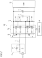
- FIG. 2 which is a circuit configuration diagram of the power conversion device
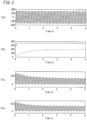
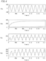
- FIG. 3 and FIG. 4 which show operation waveforms during initial charging in a comparative example
- FIG. 5 which shows voltage waveforms during initial charging of the smoothing capacitor with respect to change of the current limiting resistor
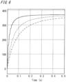
- FIG. 6 which shows voltage waveforms during initial charging of the smoothing capacitor with respect to change in the capacitance of the smoothing capacitor
- FIG. 7 which shows voltage waveforms during the initial charging of the smoothing capacitor with respect to change of the balance resistor
- FIG. 1 is a basic configuration diagram of the power conversion device
- FIG. 2 which is a circuit configuration diagram of the power conversion device
- FIG. 3 and FIG. 4 which show operation waveforms during initial charging in a comparative example
- FIG. 5 which shows voltage waveforms during initial charging of the smoothing capacitor with respect to change of the current limiting resistor
- FIG. 6 which shows voltage waveforms during initial charging of the smoothing capacitor with
- FIG. 8 which shows voltage waveforms during initial charging of the smoothing capacitor with respect to change in the capacitance of the charge/discharge capacitor
- FIG. 9 to FIG. 12 which show operation waveforms during initial charging with respect to change in an overvoltage degree index
- FIG. 13 which is a graph in which maximum voltage applied to the semiconductor switching element is plotted with respect to change in the overvoltage degree index.
- a power conversion device 1000 receives an input from an AC power supply 1, includes an inrush preventing circuit 2 including a current limiting resistor, a rectification circuit 4, a leg circuit 5, a balance resistor 6, a charge/discharge capacitor 7, and a smoothing capacitor 8, and has an output to which a load 10 is connected.
- an inrush preventing circuit 2 including a current limiting resistor, a rectification circuit 4, a leg circuit 5, a balance resistor 6, a charge/discharge capacitor 7, and a smoothing capacitor 8, and has an output to which a load 10 is connected.
- the rectification circuit 4 converts AC power from the AC power supply 1 to DC power.
- the leg circuit 5 includes an upper leg and a lower leg each formed by a series circuit of semiconductor elements.
- the balance resistor 6 is connected in parallel to the semiconductor elements of the leg circuit 5. Specific connection methods will be described in the embodiments. At least one charge/discharge capacitor 7 is connected between a connection point of the semiconductor elements in the upper leg and a connection point of the semiconductor elements in the lower leg.
- the smoothing capacitor 8 is connected to the output of the leg circuit 5, and the load 10 is connected to the smoothing capacitor 8.
- each semiconductor element includes a semiconductor switching element and a diode.
- the inrush preventing circuit 2 is located at a position after the rectification circuit 4.
- a reactor is provided on the input side and a controller for driving the leg circuit is needed.
- these are not directly relevant to the object of the present invention "to provide a power conversion device that can suppress overvoltage during initial charging when a power supply is turned on, during operation, and in a stopped state of a power converter", and therefore are omitted in the basic configuration in FIG. 1 .
- the AC power supply 1 and the load 10 are not components of the power conversion device 1000, but they are closely related and therefore are described without being separated.
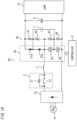
- the power conversion device 100 receives an input from a single-phase AC power supply 1a, includes the inrush preventing circuit 2 including a current limiting resistor 21 and a switch 22, the reactor 3, a diode rectification circuit 4a with only one arm including diodes 41, 42, a leg circuit 5a including a series circuit of semiconductor switching elements 51, 52 in an upper leg and a series circuit of semiconductor switching elements 53, 54 in a lower leg, a balance resistor 6a including resistors 61, 62, 63, 64, the charge/discharge capacitor 7, and the smoothing capacitor 8, and has an output to which the load 10 is connected. Further, the power conversion device 100 includes a controller 9 for driving the leg circuit 5a.
- the rectification circuit with only one arm (only one end of the single-phase AC) formed by two diodes 41, 42 as shown in FIG. 2 is described as the diode rectification circuit 4a with only one arm.
- the rectification circuit is described as a bridge rectification circuit 4b formed by four diodes, and for a three-phase AC, the rectification circuit is described as a bridge rectification circuit 4c formed by six diodes, for the purpose of discrimination.
- balance resistors When the balance resistors are collectively mentioned, they are described as the balance resistor 6a, and when each balance resistor is individually mentioned, the balance resistor is described as, for example, the balance resistor 61.
- a connection point of the anode of the diode 41 and the cathode of the diode 42 of the diode rectification circuit 4a with only one arm is connected to one end of the single-phase AC power supply 1a via the reactor 3.
- a connection point of the upper leg and the lower leg of the leg circuit 5a is connected to another end of the single-phase AC power supply 1a.
- the cathode of the diode 41 of the diode rectification circuit 4a with only one arm is connected to a positive-side DC bus of the leg circuit 5a and the anode of the diode 42 is connected to a negative-side DC bus of the leg circuit 5a.
- the balance resistors 61 to 64 are respectively connected in parallel to the semiconductor switching elements 51 to 54.
- the charge/discharge capacitor 7 is connected in parallel to a series circuit of the semiconductor switching elements 52, 53, that is, in parallel to a series circuit of the balance resistors 62, 63.
- the smoothing capacitor 8 is connected to the output of the leg circuit 5a, and the load 10 is connected to the output thereof.
- the current limiting resistor 21 can be replaced with a positive temperature coefficient (PTC) thermistor and a negative temperature coefficient (NTC) thermistor.
- PTC positive temperature coefficient
- NTC negative temperature coefficient
- the semiconductor switching elements 51 to 54 are described as metal-oxide-semiconductor field-effect transistors (MOSFET), but can be replaced with insulated-gate-bipolar-transistors (IGBT). Alternatively, semiconductor switching elements made of a new material such as SiC or GaN may be used.
- the switch 22 is turned off during initial charging operation.
- the switch 22 is turned on so that the current limiting resistor 21 is bypassed.
- the semiconductor switching elements 51 to 54 are operated by driving signals from the controller 9.
- power supply current can be made into a sinewave state and the power supply power factor can be controlled to be almost 1. Further, the charge/discharge capacitor 7 and the smoothing capacitor 8 can be controlled at desired voltage values.
- the voltage value of the charge/discharge capacitor 7 is set to 1/2 of the voltage value of the smoothing capacitor 8
- 3-level outputs can be obtained.
- the inductance value of the reactor 3 can be reduced and loss in switching of the semiconductor switching elements 51 to 54 can be reduced, as compared to a general 2-level power converter.
- the overvoltage suppression effect is high.
- the average value of the resistances of the balance resistors 61, 62, 63, 64 is denoted by Rf.
- the resistance value of the current limiting resistor 21 is denoted by R0
- the capacitance of the charge/discharge capacitor 7 is denoted by Cf
- the capacitance of the smoothing capacitor 8 is denoted by C0.
- the "average value Rf of the resistances of the balance resistors 61, 62, 63, 64" is described as a “resistance value Rf of a balance resistor", unless they particularly need to be discriminated.
- the unit of a resistance is denoted by ⁇
- the unit of a capacitance is denoted by ⁇ F
- calculation is performed using these units.
- Operation in a normal case is not limited to the above-described one.
- FIG. 3 and FIG. 4 show initial charging operation waveforms when the power supply is turned on. Operation waveforms when the power supply is turned on at time 0 are shown.
- FIG. 3 shows entire waveforms, in which F3a indicates power supply voltage of the AC power supply 1, F3b indicates voltage (solid line) of the smoothing capacitor 8 and voltage (dotted line) of the charge/discharge capacitor 7, F3c indicates voltage across the semiconductor switching element 51, and F3d indicates voltage across the semiconductor switching element 54.
- FIG. 4 shows enlarged waveforms and thus operation just after the power supply is turned on is illustrated in an enlarged manner.
- These waveforms correspond to F3a to F3d in FIG. 3 .
- F4a indicates power supply voltage of the AC power supply 1
- F4b indicates voltage (solid line) of the smoothing capacitor 8 and voltage (dotted line) of the charge/discharge capacitor 7
- F4c indicates voltage across the semiconductor switching element 51
- F4d indicates voltage across the semiconductor switching element 54.
- the smoothing capacitor 8 After the power supply is turned on, the smoothing capacitor 8 is immediately charged but the charge/discharge capacitor 7 is not immediately charged. Difference voltage between the smoothing capacitor 8 and the charge/discharge capacitor 7 is applied to the semiconductor switching element 51 and the semiconductor switching element 54.
- the charging speed of the smoothing capacitor 8 can be represented as a factor K0 by Expression (1) which is a product of R0 and C0.
- K 0 R 0 * C 0
- FIG. 5 shows comparison of charging waveforms of the smoothing capacitor 8 when the resistance value R0 of the current limiting resistor is 10 S2 (solid line), R0 is 30 S2 (dotted line), and R0 is 50 S2 (dotted-dashed line).
- the circuit constants other than the resistance value R0 of the current limiting resistor are the same among the above three conditions, that is, the resistance value Rf of the balance resistor is 100 k ⁇ , the capacitance C0 of the smoothing capacitor 8 is 1000 ⁇ F, and the capacitance Cf of the charge/discharge capacitor 7 is 10 ⁇ F.
- FIG. 6 shows comparison of charging waveforms of the smoothing capacitor 8 when the capacitance C0 of the smoothing capacitor 8 is 1000 ⁇ F (solid line), C0 is 3000 ⁇ F (dotted line), and C0 is 5000 ⁇ F (dotted-dashed line).
- the circuit constants other than the capacitance C0 of the smoothing capacitor 8 are the same among the above three conditions, that is, the resistance value R0 of the current limiting resistor is 10 ⁇ , the resistance value Rf of the balance resistor is 100 kQ, and the capacitance Cf of the charge/discharge capacitor 7 is 10 ⁇ F. Also when the capacitance C0 of the smoothing capacitor 8 is increased, the factor K0 increases and thus it is found that the charging time of the smoothing capacitor 8 is prolonged.
- the charging time is the same even if the resistance value R0 of the current limiting resistor and the capacitance C0 of the smoothing capacitor 8 are changed.
- the charging speed of the charge/discharge capacitor 7 can be represented as a factor Kf by Expression (2) which is a product of the resistance value Rf of the balance resistor and the capacitance Cf of the charge/discharge capacitor 7.
- Kf Rf * Cf
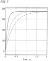
- FIG. 7 shows comparison of charging waveforms of the charge/discharge capacitor 7 when the resistance value Rf of the balance resistor is 10 k ⁇ (solid line), Rf is 30 k ⁇ (dotted line), and Rf is 50 k ⁇ (dotted-dashed line).
- the circuit constants other than the resistance value of the balance resistor are the same among the above three conditions, that is, the resistance value R0 of the current limiting resistor is 10 ⁇ , the capacitance C0 of the smoothing capacitor 8 is 1000 ⁇ F, and the capacitance Cf of the charge/discharge capacitor 7 is 10 ⁇ F.
- FIG. 8 shows comparison of charging waveforms of the charge/discharge capacitor 7 when the capacitance Cf of the charge/discharge capacitor 7 is 10 ⁇ F, Cf is 30 ⁇ F, and Cf is 50 ⁇ F.
- the circuit constants other than the capacitance of the charge/discharge capacitor 7 are the same among the above three conditions, that is, the resistance value R0 of the current limiting resistor is 10 ⁇ , the resistance value Rf of the balance resistor is 10 kQ, and the capacitance C0 of the smoothing capacitor 8 is 1000 ⁇ F.
- the charging time is the same even if the resistance value Rf of the balance resistor and the capacitance Cf of the charge/discharge capacitor 7 are changed.
- the charging speed of the smoothing capacitor 8 can be controlled by increasing/decreasing the factor K0, and the charging speed of the charge/discharge capacitor 7 can be controlled by increasing/decreasing the factor Kf.
- the overvoltage degree index can be represented as a factor Km by Expression (3).
- Km Kf / K 0
- the balance between the charging times of the smoothing capacitor 8 and the charge/discharge capacitor 7 can be expressed by the factor Km which is the overvoltage degree index. As the factor Km decreases, overshoot in initial charging of the charge/discharge capacitor 7 can be more suppressed.
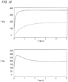
- FIG. 9 to FIG. 12 show charging characteristics of the smoothing capacitor 8 and the charge/discharge capacitor 7 when the factor Km is 100 (comparative example), Km is 20, Km is 7.5, and Km is 3.
- a solid line in F9a indicates voltage of the smoothing capacitor 8 and a dotted line indicates voltage of the charge/discharge capacitor 7.
- F9b indicates difference voltage between voltage of the smoothing capacitor 8 and voltage of the charge/discharge capacitor 7. The difference voltage is applied to the semiconductor switching elements 51, 54.
- the resistance value R0 of the current limiting resistor is increased in order to decrease the factor Km, whereby the charging speed of the smoothing capacitor 8 is made slow and thus overshoot of the semiconductor switching element applied voltage is suppressed.
- the horizontal axis indicates the factor Km and the vertical axis indicates maximum voltage [V] across the semiconductor switching element.
- the semiconductor switching elements can be formed by lower-withstanding-voltage elements. Thus, cost increase is suppressed, high-efficiency semiconductor switching elements can be selected, and a higher-efficiency power converter can be obtained.
- the power conversion device of Embodiment 1 includes the diode rectification circuit with only one arm which rectifies input voltage from the single-phase AC power supply, the leg circuit including the upper leg and the lower leg each formed by two semiconductor switching elements connected in series, the balance resistors connected in parallel to the respective semiconductor switching elements of the leg circuit, the charge/discharge capacitor connected between the connection point of the semiconductor switching elements in the upper leg and the connection point of the semiconductor switching elements in the lower leg, the smoothing capacitor connected to the output of the leg circuit, the inrush preventing circuit including the current limiting resistor between the single-phase AC power supply and the diode rectification circuit with only one arm, and the reactor.
- the power conversion device of Embodiment 1 can suppress overvoltage during initial charging when the power supply is turned on, during operation, and in a stopped state.
- a power conversion device of Embodiment 2 includes a bridge rectification circuit instead of the diode rectification circuit with only one arm.
- Embodiment 2 The configuration and operation of the power conversion device according to Embodiment 2 will be described focusing on difference from Embodiment 1, with reference to FIG. 14 which is a configuration diagram of the power conversion device and FIG. 15 and FIG. 16 which are circuit configuration diagrams in other configurations.
- the power conversion device is denoted by 200, 201, and 202.
- Embodiment 2 The difference between Embodiment 2 and Embodiment 1 is that the diode rectification circuit 4a with only one arm including two diodes is replaced with a bridge rectification circuit 4b including four diodes. Power is converted from AC to DC using the bridge rectification circuit 4b. Therefore, connection among the single-phase AC power supply 1a, the bridge rectification circuit 4b, and the leg circuit 5a is changed.
- the power conversion device 200 receives an input from the single-phase AC power supply 1a, includes the inrush preventing circuit 2 including the current limiting resistor 21 and the switch 22, the reactor 3, the bridge rectification circuit 4b, the leg circuit 5a including a series circuit of the semiconductor switching elements 51, 52 in the upper leg and a series circuit of the semiconductor switching elements 53, 54 in the lower leg, the balance resistor 6a including the resistors 61, 62, 63, 64, the charge/discharge capacitor 7, and the smoothing capacitor 8, and has an output to which the load 10 is connected. Further, the power conversion device 200 includes the controller 9 for driving the leg circuit 5a.
- the single-phase AC power supply 1a is connected to the input of the bridge rectification circuit 4b via the reactor 3.
- the output of the bridge rectification circuit 4b is connected in parallel to the lower leg formed by the series circuit of the semiconductor switching elements 53, 54 in the leg circuit 5a.
- the charging characteristics of the smoothing capacitor 8 and the charge/discharge capacitor 7 are the same as those in Embodiment 1, and therefore the function and the operation described in Embodiment 1 can be applied.
- circuit configurations shown in FIG. 15 and FIG. 16 which are modifications of the circuit configuration in FIG. 14 , also have the same function and operation as those of the power conversion device 200 in Embodiment 2.
- the power conversion device 201 has a configuration in which the semiconductor switching elements 51, 52 are replaced with diodes 51a, 52a.
- Embodiment 2 since the bridge rectification circuit 4b is used, the same operation as in the power conversion device 200 in FIG. 14 can be performed even if the semiconductor switching elements 51, 52 are replaced with elements other than semiconductor switching elements.
- Using the diodes 51a, 52a has an advantage that the cost is lower than in a case of using the semiconductor switching elements 51, 52.
- the inrush preventing circuit 2 and the reactor 3 are transferred to the output side of the bridge rectification circuit 4b. Also in this circuit configuration, the function and the operation are the same as those of the power conversion devices 200, 201.
- the semiconductor switching elements can be formed by lower-withstand-voltage elements.
- cost increase is suppressed, high-efficiency elements can be selected, and a higher-efficiency power converter can be obtained.
- the power conversion device of Embodiment 2 includes the bridge rectification circuit instead of the diode rectification circuit with only one arm.
- the power conversion device of Embodiment 2 can suppress overvoltage during initial charging when the power supply is turned on, during operation, and in a stopped state.
- a power conversion device of Embodiment 3 uses, as the AC power supply, a three-phase AC power supply.
- FIG. 17 which is a circuit configuration diagram of the power conversion device
- FIG. 18 which is a circuit configuration diagram in another configuration
- FIG. 19 to FIG. 22 which show operation waveforms during initial charging with respect to change in the overvoltage degree index
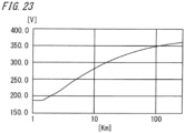
- FIG. 23 which is a graph in which maximum voltage applied to the semiconductor switching element is plotted with respect to change in the overvoltage degree index.
- the power conversion device is denoted by 300 and 301.
- Embodiment 3 The difference between Embodiment 3 and Embodiment 2 is that the single-phase AC power supply is replaced with the three-phase AC power supply. Power is converted from three-phase AC to DC using a bridge rectification circuit 4c including six diodes. Thus, connection among the three-phase AC power supply 1b, the inrush preventing circuit 2, the reactor 3, the bridge rectification circuit 4c, and the leg circuit 5a is changed.
- the power conversion device 300 receives an input from the three-phase AC power supply 1b, includes the bridge rectification circuit 4c, the inrush preventing circuit 2 including the current limiting resistor 21 and the switch 22, the reactor 3, the leg circuit 5a including a series circuit of the semiconductor switching elements 51, 52 in the upper leg and a series circuit of the semiconductor switching elements 53, 54 in the lower leg, the balance resistor 6a including the resistors 61, 62, 63, 64, the charge/discharge capacitor 7, and the smoothing capacitor 8, and has an output to which the load 10 is connected. Further, the power conversion device 300 includes the controller 9 for driving the leg circuit 5a.
- the three-phase AC power of the three-phase AC power supply 1b is converted to DC power by the bridge rectification circuit 4c which is connected, via the inrush preventing circuit 2 and the reactor 3, in parallel to the lower leg formed by the series circuit of the semiconductor switching elements 53, 54 in the leg circuit 5a.
- FIG. 18 shows a circuit configuration of the power conversion device 301 which is another configuration of the power conversion device 300. Since power is converted from AC to DC using the bridge rectification circuit 4c as described in Embodiment 2, the semiconductor switching elements 51, 51 of the upper leg of the leg circuit 5a can be replaced with the diodes 51a, 52a. Even in the case of using a leg circuit 5b, the function and the operation of the power conversion device 301 are the same as those of the power conversion device 300.
- Embodiment 3 since the power supply is changed from the single-phase AC power supply to the three-phase AC power supply, the charging speeds of the smoothing capacitor 8 and the charge/discharge capacitor 7 are changed.
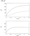
- FIG. 19 to FIG. 22 show charging characteristics of the smoothing capacitor 8 and the charge/discharge capacitor 7 when the factor Km is 100 (comparative example), Km is 10, Km is 3.7, and Km is 1.5.
- a solid line in F19a indicates voltage of the smoothing capacitor 8 and a dotted line indicates voltage of the charge/discharge capacitor 7.
- F19b indicates difference voltage between voltage of the smoothing capacitor 8 and voltage of the charge/discharge capacitor 7.
- the difference voltage is applied to the semiconductor switching element 51 (diode 51a) and the semiconductor switching element 54.
- the horizontal axis indicates the factor Km and the vertical axis indicates maximum voltage [V] across the semiconductor switching element.
- the semiconductor switching elements can be formed by lower-withstanding-voltage elements.
- cost increase is suppressed, high-efficiency elements can be selected, and a higher-efficiency power converter can be obtained.
- the power conversion device of Embodiment 3 uses, as the AC power supply, the three-phase AC power supply.
- the power conversion device of Embodiment 3 can suppress overvoltage during initial charging when the power supply is turned on, during operation, and in a stopped state.
- the balance resistor is changed to a three-resistor configuration.
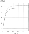
- Embodiment 4 The configuration and operation of the power conversion device according to Embodiment 4 will be described focusing on difference from Embodiment 1, with reference to FIG. 24 which is a circuit configuration diagram of the power conversion device and FIG. 25 which shows comparison of the initial charging characteristic of the charge/discharge capacitor between the three-resistor configuration and the four-resistor configuration of the power conversion device.
- the power conversion device is denoted by 400.
- Embodiment 4 difference from Embodiment 1 is that the balance resistor is changed from a four-resistor configuration to a three-resistor configuration. Specifically, four balance resistors 61 to 64 are replaced with three balance resistors 61, 64, 65.
- the power conversion device 400 receives an input from the single-phase AC power supply 1a, includes the inrush preventing circuit 2 including the current limiting resistor 21 and the switch 22, the reactor 3, the diode rectification circuit 4a with only one arm, the leg circuit 5a including a series circuit of the semiconductor switching elements 51, 52 in the upper leg and a series circuit of the semiconductor switching elements 53, 54 in the lower leg, the balance resistor 6b including the balance resistors 61, 64, 65, the charge/discharge capacitor 7, and the smoothing capacitor 8, and has an output to which the load 10 is connected. Further, the power conversion device 400 includes the controller 9 for driving the leg circuit 5a.
- the balance resistor 61 is connected in parallel to the semiconductor switching element 51, and the balance resistor 64 is connected in parallel to the semiconductor switching element 54.
- the balance resistor 65 is connected in parallel to a series circuit of the semiconductor switching elements 52, 53.
- the charge/discharge capacitor 7 is connected in parallel to the balance resistor 65 and the series circuit of the semiconductor switching elements 52, 53.
- the balance resistors 61, 64 and the balance resistor 65 need to be discriminated, the balance resistors 61, 64 are described as individual balance resistors, and the balance resistor 65 is described as a common balance resistor.
- the difference between voltage of the charge/discharge capacitor 7 and voltage of the smoothing capacitor 8 changes.
- FIG. 25 shows a result of measurement of a converged value of voltage of the charge/discharge capacitor 7 in a case where the resistance value R0 of the current limiting resistor is set at 10 ⁇ , the resistance value Rf of the balance resistor is set at 10 kQ, the capacitance Cf of the charge/discharge capacitor 7 is set at 10 ⁇ F, and the capacitance C0 of the smoothing capacitor 8 is set at 1000 ⁇ F.
- a solid line corresponds to the four-resistor configuration
- a dotted line corresponds to the three-resistor configuration.
- the converged value of voltage of the charge/discharge capacitor 7 is 187 V, but in the case where the balance resistor has the three-resistor configuration, the converged value increases to 210 V.
- a curve (solid line) in the four-resistor configuration in FIG. 25 is the same as the curve for 10 ⁇ F (solid line) in FIG. 8 .
- the value of the balance resistor 65 is set to be about 1.5 times the values of the balance resistors 61, 64.
- voltage of the charge/discharge capacitor 7 becomes 1/2 of voltage of the smoothing capacitor 8.
- the balance resistor can be changed from the four-resistor configuration to the three-resistor configuration.
- the value of the balance resistor 65 is set to be two times the values of the balance resistors 61, 64, whereby, as compared to the power conversion device of Embodiment 1 having the four-resistor configuration, the effect of reducing peak voltages applied to the semiconductor switching elements 51, 54 becomes small but the peak voltages can be reduced. Thus, overvoltage of the semiconductor switching elements 51, 54 in initial charging can be suppressed.
- the semiconductor switching elements can be formed by lower-withstand-voltage elements.
- cost increase is suppressed, high-efficiency elements can be selected, and a higher-efficiency power converter can be obtained.
- the power conversion device 400 of Embodiment 4 can be configured with three balance resistors, the power conversion device can be obtained at lower cost.
- the balance resistor is changed to the three-resistor configuration.
- the power conversion device of Embodiment 4 can suppress overvoltage during initial charging when the power supply is turned on, during operation, and in a stopped state.
- Embodiment 5 The configuration and operation of the power conversion device according to Embodiment 5 will be described focusing on difference from Embodiment 1, with reference to FIG. 26 which is a configuration diagram of the power conversion device and FIG. 27 which is a graph in which maximum voltage applied to the semiconductor switching element is plotted with respect to change in the overvoltage degree index.
- the power conversion device is denoted by 500.
- Embodiment 5 difference from Embodiment 1 is that the number of semiconductor switching elements connected in series in each of the upper leg and the lower leg of a leg circuit 5c is three. Along with this configuration change, the numbers of the balance resistors and the charge/discharge capacitors are also increased.
- the power conversion device 500 receives an input from the single-phase AC power supply 1a, includes the inrush preventing circuit 2 including the current limiting resistor 21 and the switch 22, the reactor 3, the diode rectification circuit 4a with only one arm, the leg circuit 5c including a series circuit of semiconductor switching elements 56, 51, 52 in an upper leg and a series circuit of semiconductor switching elements 53, 54, 57 in a lower leg, a balance resistor 6c including resistors 66, 61, 62, 63, 64, 67, charge/discharge capacitors 7, 7a, and the smoothing capacitor 8, and has an output to which the load 10 is connected. Further, the power conversion device 500 includes the controller 9 for driving the leg circuit 5c.
- the balance resistors 66, 61, 62 are connected in parallel to the respective semiconductor switching elements 56, 51, 52.
- the balance resistors 63, 64, 67 are connected in parallel to the respective semiconductor switching elements 53, 54, 57.
- the charge/discharge capacitor 7 is connected in parallel to a series circuit of the semiconductor switching elements 52, 53, that is, in parallel to a series circuit of the balance resistors 62, 63.
- the charge/discharge capacitor 7a is connected in parallel to a series circuit of the semiconductor switching elements 51, 52, 53, 54, that is, in parallel to a series circuit of the balance resistors 61, 62, 63, 64.
- connection among the single-phase AC power supply 1a, the inrush preventing circuit 2, the reactor 3, the diode rectification circuit 4a with only one arm, and the leg circuit 5c is basically the same as in Embodiment 1 and therefore description thereof is omitted.
- the semiconductor switching elements to which overvoltage is particularly likely to be applied are the uppermost semiconductor switching element 56 in the upper leg and the lowermost semiconductor switching element 57 in the lower leg. Difference voltage between the smoothing capacitor 8 and the charge/discharge capacitor 7a is applied to the semiconductor switching elements 56, 57. Overshoot of this voltage needs to be suppressed.
- the overvoltage suppression effect is high.
- the average value of the resistances of the balance resistors 66, 61, 62, 63, 64, 67 is denoted by Rf.
- the capacitances of the charge/discharge capacitor 7 and the charge/discharge capacitor 7a can be set at different values, but here, they are set at the same value and denoted by Cf. Further, the resistance value of the current limiting resistor 21 is denoted by R0 and the capacitance of the smoothing capacitor is denoted by C0.
- the factors Kf, K0, Km can be defined in the same manner as in Embodiment 1.
- FIG. 27 shows a graph in which the factor Km which is the overvoltage degree index and maximum voltage applied to the semiconductor switching elements 56, 57 are plotted.
- the horizontal axis indicates the factor Km and the vertical axis indicates maximum voltage [V] across the semiconductor switching element.
- a solid line shows a case where three semiconductor switching elements are connected in series in each of the upper leg and the lower leg in the power conversion device 500 of Embodiment 5.
- a dotted line shows a case where two semiconductor switching elements are connected in series in each of the upper leg and the lower leg in the power conversion device 100 of Embodiment 1.
- the semiconductor switching elements in the upper leg can be replaced with diodes as in the power conversion devices 201 ( FIG. 15 ) and 202 ( FIG. 16 ) of Embodiment 2 and the power conversion device 301 ( FIG. 18 ) of Embodiment 3.
- the number of balance resistors is decreased as in Embodiment 4, the number of semiconductor switching elements connected in series can be increased.
- the balance resistors 62, 63 may be replaced with one balance resistor, whereby the number of the balance resistors can be decreased to five.
- Embodiment 5 the case where three semiconductor switching elements connected in series in each of the upper leg and the lower leg has been described. However, a configuration of connecting four or five semiconductor switching elements in series in each of the upper leg and the lower leg may be adopted.
- the semiconductor switching elements can be formed by lower-withstand-voltage elements. Thus, cost increase is suppressed, high-efficiency semiconductor switching elements can be selected, and a higher-efficiency power converter can be obtained.
- the power conversion device of Embodiment 5 can suppress overvoltage during initial charging when the power supply is turned on, during operation, and in a stopped state.
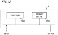
- FIG. 28 shows an example of hardware of the controller 9 of the power conversion device.
- the controller 9 is composed of a processor 2000 and a storage device 2001.
- the storage device is provided with a volatile storage device such as a random access memory and a nonvolatile auxiliary storage device such as a flash memory.
- An auxiliary storage device of a hard disk may be provided instead of the flash memory.
- the processor 2000 executes a program inputted from the storage device 2001.
- the program is inputted from the auxiliary storage device to the processor 2000 via the volatile storage device.
- the processor 2000 may output data such as a calculation result to the volatile storage device of the storage device 2001, or may store such data into the auxiliary storage device via the volatile storage device.
Landscapes
- Engineering & Computer Science (AREA)
- Power Engineering (AREA)
- Rectifiers (AREA)
- Dc-Dc Converters (AREA)
Abstract
Description
- The present disclosure relates to a power conversion device.
- As a high-efficiency circuit configuration of a power converter, a power conversion device that outputs multilevel DC power using charging/discharging of a charge/discharge capacitor is known. In the multilevel converter, voltage applied to each semiconductor element in a non-steady state does not become half of DC bus voltage, and therefore there is a problem that a low-withstanding-voltage element cannot be applied.
- For this problem, disclosed is a power conversion device that includes a reactor connected to a DC power supply on the input side, switching elements, a charge/discharge capacitor to be charged/discharged through ON/OFF operation of the switching elements, diodes for providing a charge/discharge path, balance resistors connected in parallel to the switching elements and the diodes, and an output voltage smoothing capacitor (for example, Patent Document 1).
- Patent Document 1: Japanese Laid-Open Patent Publication
JP 2014- 33 553 A - In the power conversion device in
Patent Document 1, overvoltage can be suppressed in a stopped state, but there is a problem that overvoltage is applied to the semiconductor element during initial charging when the power supply is turned on. - The present invention has been made to solve the above problem, and an object of the present invention is to provide a power conversion device that can suppress overvoltage during initial charging when a power supply is turned on, during operation, and in a stopped state.
- A power conversion device according to the present invention includes a rectification circuit which is connected to an AC power supply and rectifies input voltage from the AC power supply; a leg circuit connected to the rectification circuit and having an upper leg composed of a plurality of semiconductor elements connected in series and a lower leg composed of a plurality of semiconductor elements connected in series, the upper leg and the lower leg being connected in series, at least the plurality of semiconductor elements in the lower leg being switching elements; a balance resistor connected in parallel to the semiconductor elements of the leg circuit; at least one charge/discharge capacitor connected between a connection point of the semiconductor elements in the upper leg and a connection point of the semiconductor elements in the lower leg; a smoothing capacitor connected to an output of the leg circuit; and an inrush preventing circuit provided between the AC power supply and the leg circuit, and including a current limiting resistor.
- The power conversion device according to the present invention can suppress overvoltage during initial charging when a power supply is turned on, during operation, and in a stopped state.
-
-
FIG. 1 is a basic configuration diagram of a power conversion device according toEmbodiment 1. -
FIG. 2 is a circuit configuration diagram of the power conversion device according toEmbodiment 1. -
FIG. 3 shows operation waveforms during initial charging in a comparative example of a power conversion device according toEmbodiment 1. -
FIG. 4 shows operation waveforms during initial charging in the comparative example of the power conversion device according toEmbodiment 1. -
FIG. 5 shows voltage waveforms during initial charging of a smoothing capacitor with respect to change of a current limiting resistor in the power conversion device according toEmbodiment 1. -
FIG. 6 shows voltage waveforms during initial charging of the smoothing capacitor with respect to change in the capacitance of the smoothing capacitor in the power conversion device according toEmbodiment 1. -
FIG. 7 shows voltage waveforms during initial charging of the smoothing capacitor with respect to change of a balance resistor in the power conversion device according toEmbodiment 1. -
FIG. 8 shows voltage waveforms during initial charging of the smoothing capacitor with respect to change in the capacitance of a charge/discharge capacitor in the power conversion device according toEmbodiment 1. -
FIG. 9 shows operation waveforms during initial charging with respect to change in an overvoltage degree index in the power conversion device according toEmbodiment 1. -
FIG. 10 shows operation waveforms during initial charging with respect to change in the overvoltage degree index in the power conversion device according toEmbodiment 1. -
FIG. 11 shows operation waveforms during initial charging with respect to change in the overvoltage degree index in the power conversion device according toEmbodiment 1. -
FIG. 12 shows operation waveforms during initial charging with respect to change in the overvoltage degree index in the power conversion device according toEmbodiment 1. -
FIG. 13 is a graph in which maximum voltage applied to a semiconductor switching element is plotted with respect to change in the overvoltage degree index in the power conversion device according toEmbodiment 1. -
FIG. 14 is a circuit configuration diagram of a power conversion device according toEmbodiment 2. -
FIG. 15 is a circuit configuration diagram inanother configuration 1 of the power conversion device according toEmbodiment 2. -
FIG. 16 is a circuit configuration diagram inanother configuration 2 of the power conversion device according toEmbodiment 2. -
FIG. 17 is a circuit configuration diagram of a power conversion device according toEmbodiment 3. -
FIG. 18 is a circuit configuration diagram in another configuration of the power conversion device according toEmbodiment 3. -
FIG. 19 shows operation waveforms during initial charging with respect to change in the overvoltage degree index in the power conversion device according toEmbodiment 3. -
FIG. 20 shows operation waveforms during initial charging with respect to change in the overvoltage degree index in the power conversion device according toEmbodiment 3. -
FIG. 21 shows operation waveforms during initial charging with respect to change in the overvoltage degree index in the power conversion device according toEmbodiment 3. -
FIG. 22 shows operation waveforms during initial charging with respect to change in the overvoltage degree index in the power conversion device according toEmbodiment 3. -
FIG. 23 is a graph in which maximum voltage applied to the semiconductor switching element is plotted with respect to change in the overvoltage degree index in the power conversion device according toEmbodiment 3. -
FIG. 24 is a circuit configuration diagram of a power conversion device according toEmbodiment 4. -
FIG. 25 shows comparison of the initial charging characteristic of the charge/discharge capacitor between a three-resistor configuration and a four-resistor configuration in the power conversion device according toEmbodiment 4. -
FIG. 26 is a circuit configuration diagram of a power conversion device according toEmbodiment 5. -
FIG. 27 is a graph in which maximum voltage applied to the semiconductor switching element is plotted with respect to change in the overvoltage degree index in the power conversion device according toEmbodiment 5. -
FIG. 28 is a block diagram showing a hardware configuration example of a controller of the power conversion device. -
Embodiment 1 relates to a power conversion device including a diode rectification circuit with only one arm which rectifies input voltage from a single-phase AC power supply, a leg circuit including an upper leg and a lower leg each formed by two semiconductor switching elements connected in series, balance resistors connected in parallel to the respective semiconductor switching elements of the leg circuit, a charge/discharge capacitor connected between a connection point of the semiconductor switching elements in the upper leg and a connection point of the semiconductor switching elements in the lower leg, a smoothing capacitor connected to the output of the leg circuit, an inrush preventing circuit including a current limiting resistor between the single-phase AC power supply and the diode rectification circuit with only one arm, and a reactor. - Hereinafter, the configuration and operation of the power conversion device according to
Embodiment 1 will be described with reference toFIG. 1 which is a basic configuration diagram of the power conversion device,FIG. 2 which is a circuit configuration diagram of the power conversion device,FIG. 3 andFIG. 4 which show operation waveforms during initial charging in a comparative example,FIG. 5 which shows voltage waveforms during initial charging of the smoothing capacitor with respect to change of the current limiting resistor,FIG. 6 which shows voltage waveforms during initial charging of the smoothing capacitor with respect to change in the capacitance of the smoothing capacitor,FIG. 7 which shows voltage waveforms during the initial charging of the smoothing capacitor with respect to change of the balance resistor,FIG. 8 which shows voltage waveforms during initial charging of the smoothing capacitor with respect to change in the capacitance of the charge/discharge capacitor,FIG. 9 to FIG. 12 which show operation waveforms during initial charging with respect to change in an overvoltage degree index, andFIG. 13 which is a graph in which maximum voltage applied to the semiconductor switching element is plotted with respect to change in the overvoltage degree index. - Before describing the configuration of a
power conversion device 100 ofEmbodiment 1 with reference toFIG. 2 , the basic configuration thereof which is common among the power conversion devices ofEmbodiment 1 and thesubsequent embodiments 2, and so forth, will be described with reference toFIG. 1 . - A
power conversion device 1000 receives an input from anAC power supply 1, includes aninrush preventing circuit 2 including a current limiting resistor, arectification circuit 4, aleg circuit 5, a balance resistor 6, a charge/discharge capacitor 7, and asmoothing capacitor 8, and has an output to which aload 10 is connected. - Here, the
rectification circuit 4 converts AC power from theAC power supply 1 to DC power. Theleg circuit 5 includes an upper leg and a lower leg each formed by a series circuit of semiconductor elements. - The balance resistor 6 is connected in parallel to the semiconductor elements of the
leg circuit 5. Specific connection methods will be described in the embodiments. At least one charge/discharge capacitor 7 is connected between a connection point of the semiconductor elements in the upper leg and a connection point of the semiconductor elements in the lower leg. - The
smoothing capacitor 8 is connected to the output of theleg circuit 5, and theload 10 is connected to thesmoothing capacitor 8. - Here, each semiconductor element includes a semiconductor switching element and a diode.
- In a case where the
AC power supply 1 is a three-phase AC power supply, theinrush preventing circuit 2 is located at a position after therectification circuit 4. - Generally, in the power conversion device, a reactor is provided on the input side and a controller for driving the leg circuit is needed. However, these are not directly relevant to the object of the present invention "to provide a power conversion device that can suppress overvoltage during initial charging when a power supply is turned on, during operation, and in a stopped state of a power converter", and therefore are omitted in the basic configuration in
FIG. 1 . - The
AC power supply 1 and theload 10 are not components of thepower conversion device 1000, but they are closely related and therefore are described without being separated. - Next, the configuration of a
power conversion device 100 shown inFIG. 2 will be described. - The
power conversion device 100 receives an input from a single-phaseAC power supply 1a, includes theinrush preventing circuit 2 including a current limitingresistor 21 and aswitch 22, thereactor 3, adiode rectification circuit 4a with only onearm including diodes leg circuit 5a including a series circuit ofsemiconductor switching elements semiconductor switching elements balance resistor 6a including resistors discharge capacitor 7, and thesmoothing capacitor 8, and has an output to which theload 10 is connected. Further, thepower conversion device 100 includes acontroller 9 for driving theleg circuit 5a. - The rectification circuit with only one arm (only one end of the single-phase AC) formed by two
diodes FIG. 2 is described as thediode rectification circuit 4a with only one arm. For a single-phase AC described in other embodiments, the rectification circuit is described as abridge rectification circuit 4b formed by four diodes, and for a three-phase AC, the rectification circuit is described as abridge rectification circuit 4c formed by six diodes, for the purpose of discrimination. - When the balance resistors are collectively mentioned, they are described as the
balance resistor 6a, and when each balance resistor is individually mentioned, the balance resistor is described as, for example, thebalance resistor 61. - A connection point of the anode of the
diode 41 and the cathode of thediode 42 of thediode rectification circuit 4a with only one arm is connected to one end of the single-phaseAC power supply 1a via thereactor 3. A connection point of the upper leg and the lower leg of theleg circuit 5a is connected to another end of the single-phaseAC power supply 1a. The cathode of thediode 41 of thediode rectification circuit 4a with only one arm is connected to a positive-side DC bus of theleg circuit 5a and the anode of thediode 42 is connected to a negative-side DC bus of theleg circuit 5a. - The
balance resistors 61 to 64 are respectively connected in parallel to thesemiconductor switching elements 51 to 54. The charge/discharge capacitor 7 is connected in parallel to a series circuit of thesemiconductor switching elements balance resistors capacitor 8 is connected to the output of theleg circuit 5a, and theload 10 is connected to the output thereof. - The current limiting
resistor 21 can be replaced with a positive temperature coefficient (PTC) thermistor and a negative temperature coefficient (NTC) thermistor. Thesemiconductor switching elements 51 to 54 are described as metal-oxide-semiconductor field-effect transistors (MOSFET), but can be replaced with insulated-gate-bipolar-transistors (IGBT). Alternatively, semiconductor switching elements made of a new material such as SiC or GaN may be used. - In the
power conversion device 100, theswitch 22 is turned off during initial charging operation. When the initial charging operation described later in detail is completed, theswitch 22 is turned on so that the current limitingresistor 21 is bypassed. Then, thesemiconductor switching elements 51 to 54 are operated by driving signals from thecontroller 9. - With the
semiconductor switching elements 51 to 54 subjected to appropriate switching control by driving signals from thecontroller 9, power supply current can be made into a sinewave state and the power supply power factor can be controlled to be almost 1. Further, the charge/discharge capacitor 7 and the smoothingcapacitor 8 can be controlled at desired voltage values. - In particular, when the voltage value of the charge/
discharge capacitor 7 is set to 1/2 of the voltage value of the smoothingcapacitor 8, 3-level outputs can be obtained. In the case of 3-level outputs, the inductance value of thereactor 3 can be reduced and loss in switching of thesemiconductor switching elements 51 to 54 can be reduced, as compared to a general 2-level power converter. - If the
balance resistors balance resistors - Further, the resistance value of the current limiting
resistor 21 is denoted by R0, the capacitance of the charge/discharge capacitor 7 is denoted by Cf, and the capacitance of the smoothingcapacitor 8 is denoted by C0. - In the following description, the "average value Rf of the resistances of the
balance resistors - The unit of a resistance is denoted by Ω, the unit of a capacitance is denoted by µF, and calculation is performed using these units.
- Here, operation of the
power conversion device 100 shown inFIG. 2 in a normal case will be described. In thepower conversion device 100 shown inFIG. 2 , operation is switched in accordance with whether AC voltage outputted from theAC power supply 1 is positive or negative. - When AC voltage outputted from the
AC power supply 1 is positive, thesemiconductor switching elements discharge capacitor 7 so as to charge the charge/discharge capacitor 7, a path for discharging the charge/discharge capacitor 7, and a path on which current does not flow through the charge/discharge capacitor 7. Through the above switching, input voltage from theAC power supply 1 is boosted and the boosted voltage is outputted to the smoothingcapacitor 8 side. - When AC voltage outputted from the
AC power supply 1 is negative, thesemiconductor switching elements AC power supply 1 is boosted and the boosted voltage is outputted to the smoothingcapacitor 8 side. - Operation in a normal case is not limited to the above-described one.
- Next, initial charging operation for the charge/
discharge capacitor 7 and the smoothingcapacitor 8 when the power supply is turned on will be described with reference toFIG. 3 to FIG. 13 . - First, initial charging operation in a comparative example will be described. Circuit constants are set as follows: the resistance value R0 of the current limiting resistor = 10 Ω, the resistance value Rf of the balance resistor = 100 kQ, the capacitance C0 of the smoothing
capacitor 8 = 1000 µF, and the capacitance Cf of the charge/discharge capacitor 7 = 10 µF. -
FIG. 3 andFIG. 4 show initial charging operation waveforms when the power supply is turned on. Operation waveforms when the power supply is turned on attime 0 are shown. -
FIG. 3 shows entire waveforms, in which F3a indicates power supply voltage of theAC power supply 1, F3b indicates voltage (solid line) of the smoothingcapacitor 8 and voltage (dotted line) of the charge/discharge capacitor 7, F3c indicates voltage across thesemiconductor switching element 51, and F3d indicates voltage across thesemiconductor switching element 54. - Actual waveforms of F3a, F3c, F3d in
FIG. 3 are denser and thus cannot be recognized as sine waveforms, but waveforms inFIG. 3 are shown coarsely for facilitating the understanding. -
FIG. 4 shows enlarged waveforms and thus operation just after the power supply is turned on is illustrated in an enlarged manner. These waveforms correspond to F3a to F3d inFIG. 3 . Specifically, F4a indicates power supply voltage of theAC power supply 1, F4b indicates voltage (solid line) of the smoothingcapacitor 8 and voltage (dotted line) of the charge/discharge capacitor 7, F4c indicates voltage across thesemiconductor switching element 51, and F4d indicates voltage across thesemiconductor switching element 54. - After the power supply is turned on, the smoothing
capacitor 8 is immediately charged but the charge/discharge capacitor 7 is not immediately charged. Difference voltage between the smoothingcapacitor 8 and the charge/discharge capacitor 7 is applied to thesemiconductor switching element 51 and thesemiconductor switching element 54. - Voltage applied at the time of power supply turn-on operation causes overshoot and thus an overvoltage period arises. In a case where this state arises, the semiconductor switching element cannot be formed by a low-withstanding-voltage element, and this is disadvantageous in terms of efficiency improvement and cost reduction.
- In order to prevent such an overvoltage phenomenon, it is necessary to make a charging time of the smoothing
capacitor 8 slow or make a charging time of the charge/discharge capacitor 7 fast, so as to suppress voltage overshoot. - Here, a method for suppressing overvoltage in initial charging will be described.
- The charging speed of the smoothing
capacitor 8 can be represented as a factor K0 by Expression (1) which is a product of R0 and C0.
- As the factor K0 increases, the charging time is prolonged, and as the factor K0 decreases, the charging time is shortened.
FIG. 5 shows comparison of charging waveforms of the smoothingcapacitor 8 when the resistance value R0 of the current limiting resistor is 10 S2 (solid line), R0 is 30 S2 (dotted line), and R0 is 50 S2 (dotted-dashed line). - The circuit constants other than the resistance value R0 of the current limiting resistor are the same among the above three conditions, that is, the resistance value Rf of the balance resistor is 100 kΩ, the capacitance C0 of the smoothing
capacitor 8 is 1000 µF, and the capacitance Cf of the charge/discharge capacitor 7 is 10 µF. - When the resistance value R0 of the current limiting resistor is increased, K0 increases and thus it is found that the charging time of the smoothing
capacitor 8 is prolonged. - Increasing the capacitance C0 of the smoothing
capacitor 8 can also make the charging time slow.FIG. 6 shows comparison of charging waveforms of the smoothingcapacitor 8 when the capacitance C0 of the smoothingcapacitor 8 is 1000 µF (solid line), C0 is 3000 µF (dotted line), and C0 is 5000 µF (dotted-dashed line). - The circuit constants other than the capacitance C0 of the smoothing
capacitor 8 are the same among the above three conditions, that is, the resistance value R0 of the current limiting resistor is 10 Ω, the resistance value Rf of the balance resistor is 100 kQ, and the capacitance Cf of the charge/discharge capacitor 7 is 10 µF. Also when the capacitance C0 of the smoothingcapacitor 8 is increased, the factor K0 increases and thus it is found that the charging time of the smoothingcapacitor 8 is prolonged. - When the factor K0 is the same value, the charging time is the same even if the resistance value R0 of the current limiting resistor and the capacitance C0 of the smoothing
capacitor 8 are changed. - The charging speed of the charge/
discharge capacitor 7 can be represented as a factor Kf by Expression (2) which is a product of the resistance value Rf of the balance resistor and the capacitance Cf of the charge/discharge capacitor 7.
- As the factor Kf increases, the charging time is prolonged, and as the factor Kf decreases, the charging time is shortened.
-
FIG. 7 shows comparison of charging waveforms of the charge/discharge capacitor 7 when the resistance value Rf of the balance resistor is 10 kΩ (solid line), Rf is 30 kΩ (dotted line), and Rf is 50 kΩ (dotted-dashed line). - The circuit constants other than the resistance value of the balance resistor are the same among the above three conditions, that is, the resistance value R0 of the current limiting resistor is 10 Ω, the capacitance C0 of the smoothing
capacitor 8 is 1000 µF, and the capacitance Cf of the charge/discharge capacitor 7 is 10 µF. - When the resistance value Rf of the balance resistor is increased, the factor Kf increases and thus it is found that the charging time is prolonged.
- It should be noted that, if the resistance value Rf of the balance resistor is excessively decreased, loss in the balance resistor increases, though the charging time is shortened.
- Increasing the capacitance Cf of the charge/
discharge capacitor 7 can also make the charging time slow.FIG. 8 shows comparison of charging waveforms of the charge/discharge capacitor 7 when the capacitance Cf of the charge/discharge capacitor 7 is 10 µF, Cf is 30 µF, and Cf is 50 µF. - The circuit constants other than the capacitance of the charge/
discharge capacitor 7 are the same among the above three conditions, that is, the resistance value R0 of the current limiting resistor is 10 Ω, the resistance value Rf of the balance resistor is 10 kQ, and the capacitance C0 of the smoothingcapacitor 8 is 1000 µF. - Also when the capacitance Cf of the charge/
discharge capacitor 7 is increased, the factor Kf increases and thus it is found that the charging time is prolonged. - When the factor Kf is the same value, the charging time is the same even if the resistance value Rf of the balance resistor and the capacitance Cf of the charge/
discharge capacitor 7 are changed. - The charging speed of the smoothing
capacitor 8 can be controlled by increasing/decreasing the factor K0, and the charging speed of the charge/discharge capacitor 7 can be controlled by increasing/decreasing the factor Kf. - As described above, in the circuit configuration of the
power conversion device 100 ofEmbodiment 1, decreasing the factor Kf and increasing the factor K0 is effective for suppressing overvoltage applied to thesemiconductor switching elements 51 to 54 in initial charging. - Here, the overvoltage degree index can be represented as a factor Km by Expression (3).

- The balance between the charging times of the smoothing
capacitor 8 and the charge/discharge capacitor 7 can be expressed by the factor Km which is the overvoltage degree index. As the factor Km decreases, overshoot in initial charging of the charge/discharge capacitor 7 can be more suppressed. -
FIG. 9 to FIG. 12 show charging characteristics of the smoothingcapacitor 8 and the charge/discharge capacitor 7 when the factor Km is 100 (comparative example), Km is 20, Km is 7.5, and Km is 3. -
FIG. 9 corresponds to the case of the factor Km = 100,FIG. 10 corresponds to the case of the factor Km = 20,FIG. 11 corresponds to the case of the factor Km = 7.5, andFIG. 12 corresponds to the case of the factor Km = 3. - In
FIG. 9 to FIG. 12 , a solid line in F9a (F10a, F11a, F12a) indicates voltage of the smoothingcapacitor 8 and a dotted line indicates voltage of the charge/discharge capacitor 7. - In
FIG. 9 to FIG. 12 , F9b (F10b, F11b, F12b) indicates difference voltage between voltage of the smoothingcapacitor 8 and voltage of the charge/discharge capacitor 7. The difference voltage is applied to thesemiconductor switching elements - The voltage exceeds 300 V in the case of the factor Km = 100 in the comparative example, but it is found that, when the factor Km is decreased, the overshoot voltage is suppressed.
- Since the peak value of AC voltage of the single-phase
AC power supply 1a inEmbodiment 1 is 374 V, a converged value of voltage of the smoothingcapacitor 8 is 374 V and a converged value of voltage of the charge/discharge capacitor 7 is 187 V. - In the condition of the factor Km = 20, the peak value of the semiconductor switching element applied voltage is 280 V and overshoot of the semiconductor switching element applied voltage decreases to 280/187 = 1.5 times. It can be confirmed that the peak value of the semiconductor switching element applied voltage is suppressed and thus the effect of the
power conversion device 100 ofEmbodiment 1 is exhibited. - Further, when the factor Km is decreased to 7.5, the peak value of the semiconductor switching element applied voltage becomes 234 V and the overshoot decreases to
234/187 = 1.25 times. Thus, it can be confirmed that the effect of thepower conversion device 100 ofEmbodiment 1 is further exhibited. - Further, when the factor Km is decreased to 3, overshoot of the semiconductor switching element applied voltage almost disappears. Thus, the effect of the
power conversion device 100 ofEmbodiment 1 can be maximally exhibited. - In the above analysis, the resistance value R0 of the current limiting resistor is increased in order to decrease the factor Km, whereby the charging speed of the smoothing
capacitor 8 is made slow and thus overshoot of the semiconductor switching element applied voltage is suppressed. - However, it is also possible to suppress overshoot of the semiconductor switching element applied voltage by decreasing the resistance value Rf of the balance resistor and making the charging speed of the charge/
discharge capacitor 7 fast. - In addition, it is also possible to adjust the charging time by adjusting the capacitance C0 of the smoothing
capacitor 8 and the capacitance Cf of the charge/discharge capacitor 7. However, the capacitances of the capacitors influence operation of the converter and the capacitors are more expensive components than the resistors. Therefore, the degree of freedom in selecting the capacitors is small as compared to the resistors. - When the factor Km and the peak value of the semiconductor switching element applied voltage are represented as a graph, a relationship shown in
FIG. 13 is obtained. - In
FIG. 13 , the horizontal axis indicates the factor Km and the vertical axis indicates maximum voltage [V] across the semiconductor switching element. - It is clear that, as the factor Km decreases, the peak voltage can be more suppressed.
- When the
balance resistors power conversion device 100 ofEmbodiment 1 increases. However, even if the resistance values of the balance resistors vary by about 10% to 20%, the effect is sufficiently obtained. - In the power conversion device of
Embodiment 1, overvoltage of thesemiconductor switching elements - In the
power conversion device 100 ofEmbodiment 1, since overvoltage can be suppressed in initial charging, the semiconductor switching elements can be formed by lower-withstanding-voltage elements. Thus, cost increase is suppressed, high-efficiency semiconductor switching elements can be selected, and a higher-efficiency power converter can be obtained. - As described above, the power conversion device of
Embodiment 1 includes the diode rectification circuit with only one arm which rectifies input voltage from the single-phase AC power supply, the leg circuit including the upper leg and the lower leg each formed by two semiconductor switching elements connected in series, the balance resistors connected in parallel to the respective semiconductor switching elements of the leg circuit, the charge/discharge capacitor connected between the connection point of the semiconductor switching elements in the upper leg and the connection point of the semiconductor switching elements in the lower leg, the smoothing capacitor connected to the output of the leg circuit, the inrush preventing circuit including the current limiting resistor between the single-phase AC power supply and the diode rectification circuit with only one arm, and the reactor. - Thus, the power conversion device of
Embodiment 1 can suppress overvoltage during initial charging when the power supply is turned on, during operation, and in a stopped state. - A power conversion device of
Embodiment 2 includes a bridge rectification circuit instead of the diode rectification circuit with only one arm. - The configuration and operation of the power conversion device according to
Embodiment 2 will be described focusing on difference fromEmbodiment 1, with reference toFIG. 14 which is a configuration diagram of the power conversion device andFIG. 15 andFIG. 16 which are circuit configuration diagrams in other configurations. - In
FIG. 14 to FIG. 16 inEmbodiment 2, the same or corresponding parts as those inEmbodiment 1 are denoted by the same reference characters. - For discrimination from
Embodiment 1, the power conversion device is denoted by 200, 201, and 202. - The difference between
Embodiment 2 andEmbodiment 1 is that thediode rectification circuit 4a with only one arm including two diodes is replaced with abridge rectification circuit 4b including four diodes. Power is converted from AC to DC using thebridge rectification circuit 4b. Therefore, connection among the single-phaseAC power supply 1a, thebridge rectification circuit 4b, and theleg circuit 5a is changed. - The
power conversion device 200 receives an input from the single-phaseAC power supply 1a, includes theinrush preventing circuit 2 including the current limitingresistor 21 and theswitch 22, thereactor 3, thebridge rectification circuit 4b, theleg circuit 5a including a series circuit of thesemiconductor switching elements semiconductor switching elements balance resistor 6a including theresistors discharge capacitor 7, and the smoothingcapacitor 8, and has an output to which theload 10 is connected. Further, thepower conversion device 200 includes thecontroller 9 for driving theleg circuit 5a. - The single-phase
AC power supply 1a is connected to the input of thebridge rectification circuit 4b via thereactor 3. The output of thebridge rectification circuit 4b is connected in parallel to the lower leg formed by the series circuit of thesemiconductor switching elements leg circuit 5a. - Connection between the
leg circuit 5a, and thebalance resistors 61 to 64, the charge/discharge capacitor 7, and the smoothingcapacitor 8, is the same as inEmbodiment 1, and therefore description thereof is omitted. - Also in the configuration in
FIG. 14 inEmbodiment 2, the charging characteristics of the smoothingcapacitor 8 and the charge/discharge capacitor 7 are the same as those inEmbodiment 1, and therefore the function and the operation described inEmbodiment 1 can be applied. - In addition, the circuit configurations shown in
FIG. 15 andFIG. 16 , which are modifications of the circuit configuration inFIG. 14 , also have the same function and operation as those of thepower conversion device 200 inEmbodiment 2. - As shown in
FIG. 15 , thepower conversion device 201 has a configuration in which thesemiconductor switching elements diodes - In
Embodiment 2, since thebridge rectification circuit 4b is used, the same operation as in thepower conversion device 200 inFIG. 14 can be performed even if thesemiconductor switching elements - Using the
diodes semiconductor switching elements - In the
power conversion device 202, as shown inFIG. 16 , theinrush preventing circuit 2 and thereactor 3 are transferred to the output side of thebridge rectification circuit 4b. Also in this circuit configuration, the function and the operation are the same as those of thepower conversion devices - In the
power conversion device 200 ofEmbodiment 2, overvoltage of the semiconductor switching element 51 (diode 51a) and thesemiconductor switching element 54 in initial charging can be suppressed. - In the
power conversion device 200 ofEmbodiment 2, since overvoltage can be suppressed in initial charging, the semiconductor switching elements can be formed by lower-withstand-voltage elements. Thus, cost increase is suppressed, high-efficiency elements can be selected, and a higher-efficiency power converter can be obtained. - As described above, the power conversion device of
Embodiment 2 includes the bridge rectification circuit instead of the diode rectification circuit with only one arm. - Thus, the power conversion device of
Embodiment 2 can suppress overvoltage during initial charging when the power supply is turned on, during operation, and in a stopped state. - A power conversion device of
Embodiment 3 uses, as the AC power supply, a three-phase AC power supply. - The configuration and operation of the power conversion device according to
Embodiment 3 will be described focusing on difference fromembodiments FIG. 17 which is a circuit configuration diagram of the power conversion device,FIG. 18 which is a circuit configuration diagram in another configuration,FIG. 19 to FIG. 22 which show operation waveforms during initial charging with respect to change in the overvoltage degree index, andFIG. 23 which is a graph in which maximum voltage applied to the semiconductor switching element is plotted with respect to change in the overvoltage degree index. - In
FIG. 17 andFIG. 18 inEmbodiment 3, the same or corresponding parts as those inembodiments - For discrimination from
embodiments - The difference between
Embodiment 3 andEmbodiment 2 is that the single-phase AC power supply is replaced with the three-phase AC power supply. Power is converted from three-phase AC to DC using abridge rectification circuit 4c including six diodes. Thus, connection among the three-phaseAC power supply 1b, theinrush preventing circuit 2, thereactor 3, thebridge rectification circuit 4c, and theleg circuit 5a is changed. - The
power conversion device 300 receives an input from the three-phaseAC power supply 1b, includes thebridge rectification circuit 4c, theinrush preventing circuit 2 including the current limitingresistor 21 and theswitch 22, thereactor 3, theleg circuit 5a including a series circuit of thesemiconductor switching elements semiconductor switching elements balance resistor 6a including theresistors discharge capacitor 7, and the smoothingcapacitor 8, and has an output to which theload 10 is connected. Further, thepower conversion device 300 includes thecontroller 9 for driving theleg circuit 5a. - The three-phase AC power of the three-phase
AC power supply 1b is converted to DC power by thebridge rectification circuit 4c which is connected, via theinrush preventing circuit 2 and thereactor 3, in parallel to the lower leg formed by the series circuit of thesemiconductor switching elements leg circuit 5a. - Connection between the
leg circuit 5a, and thebalance resistors 61 to 64, the charge/discharge capacitor 7, and the smoothingcapacitor 8, is the same as inembodiments -
FIG. 18 shows a circuit configuration of thepower conversion device 301 which is another configuration of thepower conversion device 300. Since power is converted from AC to DC using thebridge rectification circuit 4c as described inEmbodiment 2, thesemiconductor switching elements leg circuit 5a can be replaced with thediodes leg circuit 5b, the function and the operation of thepower conversion device 301 are the same as those of thepower conversion device 300. - In
Embodiment 3, since the power supply is changed from the single-phase AC power supply to the three-phase AC power supply, the charging speeds of the smoothingcapacitor 8 and the charge/discharge capacitor 7 are changed. - In the case of the three-phase AC power supply, DC voltage at the output of the
bridge rectification circuit 4c has a greater average value than in the case of the single-phase AC power supply. Therefore, the charging time of the smoothingcapacitor 8 becomes fast. Thus, an effective value of the factor Km is different from those in
Embodiments 1 and 2. -
FIG. 19 to FIG. 22 show charging characteristics of the smoothingcapacitor 8 and the charge/discharge capacitor 7 when the factor Km is 100 (comparative example), Km is 10, Km is 3.7, and Km is 1.5. -
FIG. 19 corresponds to the case of the factor Km = 100,FIG. 20 corresponds to the case of the factor Km = 10,FIG. 21 corresponds to the case of the factor Km = 3.7, andFIG. 22 corresponds to the case of the factor Km = 1.5. - In
FIG. 19 to FIG. 22 , a solid line in F19a (F20a, F21a, F22a) indicates voltage of the smoothingcapacitor 8 and a dotted line indicates voltage of the charge/discharge capacitor 7. - In
FIG. 19 to FIG. 22 , F19b (F20b, F21b, F22b) indicates difference voltage between voltage of the smoothingcapacitor 8 and voltage of the charge/discharge capacitor 7. The difference voltage is applied to the semiconductor switching element 51 (diode 51a) and thesemiconductor switching element 54. - The voltage exceeds 300 V in the case of the factor Km = 100 in the comparative example, but it is found that, when the factor Km is decreased, the overshoot voltage is suppressed.
- Since the peak value of AC voltage of the three-phase AC power supply in
Embodiment 3 is 374 V, a converged value of voltage of the smoothingcapacitor 8 is 374 V and a converged value of voltage of the charge/discharge capacitor 7 is 187 V. - In the condition of the factor Km = 10, the peak value of voltage of the charge/
discharge capacitor 7 is 280 V and overshoot of the semiconductor switching element applied voltage decreases to 280/187 = 1.5 times. It can be confirmed that the peak value of the semiconductor switching element applied voltage is suppressed and thus the effect of thepower conversion device 300 ofEmbodiment 3 is exhibited. - Further, when the factor Km is decreased to 3.7, the peak value of the semiconductor switching element applied voltage becomes 234 V and the overshoot of voltage decreases to 234/187 = 1.25 times. Thus, it can be confirmed that the effect of the
power conversion device 300 ofEmbodiment 3 is further exhibited. - Further, when the factor Km is decreased to 1.5, overshoot of the semiconductor switching element applied voltage almost disappears. Thus, the effect of the
power conversion device 300 ofEmbodiment 3 can be maximally exhibited. - When the factor Km and the peak value of the semiconductor switching element applied voltage are represented as a graph, a relationship shown in
FIG. 23 is obtained. - In
FIG. 23 , the horizontal axis indicates the factor Km and the vertical axis indicates maximum voltage [V] across the semiconductor switching element. - It is clear that, as the factor Km decreases, the peak voltage can be more suppressed. It is found that, when the factor Km is set to be 1/2 as compared to
Embodiment 1, the same effect as inEmbodiment 1 can be obtained. - In the power conversion device of
Embodiment 3, overvoltage of the semiconductor switching element 51 (diode 51a) and thesemiconductor switching element 54 in initial charging is suppressed. - In the
power conversion device 300 ofEmbodiment 3, since overvoltage can be suppressed in initial charging, the semiconductor switching elements can be formed by lower-withstanding-voltage elements. Thus, cost increase is suppressed, high-efficiency elements can be selected, and a higher-efficiency power converter can be obtained. - As described above, the power conversion device of
Embodiment 3 uses, as the AC power supply, the three-phase AC power supply. - Thus, the power conversion device of
Embodiment 3 can suppress overvoltage during initial charging when the power supply is turned on, during operation, and in a stopped state. - In a power conversion device of
Embodiment 4, the balance resistor is changed to a three-resistor configuration. - The configuration and operation of the power conversion device according to
Embodiment 4 will be described focusing on difference fromEmbodiment 1, with reference toFIG. 24 which is a circuit configuration diagram of the power conversion device andFIG. 25 which shows comparison of the initial charging characteristic of the charge/discharge capacitor between the three-resistor configuration and the four-resistor configuration of the power conversion device. - In
FIG. 24 inEmbodiment 4, the same or corresponding parts as those inEmbodiment 1 are denoted by the same reference characters. - For discrimination from
Embodiment 1, the power conversion device is denoted by 400. - In
Embodiment 4, difference fromEmbodiment 1 is that the balance resistor is changed from a four-resistor configuration to a three-resistor configuration. Specifically, fourbalance resistors 61 to 64 are replaced with threebalance resistors - The
power conversion device 400 receives an input from the single-phaseAC power supply 1a, includes theinrush preventing circuit 2 including the current limitingresistor 21 and theswitch 22, thereactor 3, thediode rectification circuit 4a with only one arm, theleg circuit 5a including a series circuit of thesemiconductor switching elements semiconductor switching elements balance resistor 6b including thebalance resistors discharge capacitor 7, and the smoothingcapacitor 8, and has an output to which theload 10 is connected. Further, thepower conversion device 400 includes thecontroller 9 for driving theleg circuit 5a. - Connection among the
leg circuit 5a, thebalance resistor 6b, and the charge/discharge capacitor 7 will be described. - The
balance resistor 61 is connected in parallel to thesemiconductor switching element 51, and thebalance resistor 64 is connected in parallel to thesemiconductor switching element 54. Thebalance resistor 65 is connected in parallel to a series circuit of thesemiconductor switching elements - The charge/
discharge capacitor 7 is connected in parallel to thebalance resistor 65 and the series circuit of thesemiconductor switching elements - Connection among the single-phase
AC power supply 1a, theinrush preventing circuit 2, thereactor 3, thediode rectification circuit 4a with only one arm, and theleg circuit 5a is the same as inEmbodiment 1 and therefore description thereof is omitted. - When the
balance resistors balance resistor 65 need to be discriminated, thebalance resistors balance resistor 65 is described as a common balance resistor. - Also in the
power conversion device 400 ofEmbodiment 4 in which the balance resistor is changed to the three-resistor configuration, it is possible to suppress overshoot of the semiconductor switching element applied voltage by setting the factor Km to be small. - Depending on the relationship of the values of the
balance resistors balance resistor 65, the difference between voltage of the charge/discharge capacitor 7 and voltage of the smoothingcapacitor 8 changes. - It is inferred that, when the value of the
balance resistor 65 is set to be two times the values of thebalance resistors discharge capacitor 7 becomes 1/2 of voltage of the smoothingcapacitor 8. -
FIG. 25 shows a result of measurement of a converged value of voltage of the charge/discharge capacitor 7 in a case where the resistance value R0 of the current limiting resistor is set at 10 Ω, the resistance value Rf of the balance resistor is set at 10 kQ, the capacitance Cf of the charge/discharge capacitor 7 is set at 10 µF, and the capacitance C0 of the smoothingcapacitor 8 is set at 1000 µF. - In
FIG. 25 , a solid line corresponds to the four-resistor configuration, and a dotted line corresponds to the three-resistor configuration. - In the case where the balance resistor has the four-resistor configuration, the converged value of voltage of the charge/
discharge capacitor 7 is 187 V, but in the case where the balance resistor has the three-resistor configuration, the converged value increases to 210 V. This is relevant to a configuration in which the charge/discharge capacitor 7 is charged from the AC power supply side. A curve (solid line) in the four-resistor configuration inFIG. 25 is the same as the curve for 10 µF (solid line) inFIG. 8 . - In a case of desiring to make voltage of the charge/
discharge capacitor 7 be 1/2 of voltage of the smoothing capacitor, the value of thebalance resistor 65 is set to be about 1.5 times the values of thebalance resistors discharge capacitor 7 becomes 1/2 of voltage of the smoothingcapacitor 8. - However, in the case where the above setting is made, there is a problem that voltage of the charge/
discharge capacitor 7 does not become 1/2 of voltage of the smoothingcapacitor 8 when the AC power supply side is interrupted by a circuit breaker or the like. - Therefore, in usage where both conditions at the time of turning on the power supply and at the time of interrupting the power supply need to be considered, adopting the four-resistor configuration having four balance resistors as in
embodiments 1 to 3 provides a higher effect of suppressing overvoltage. - Also in the configurations of the power conversion devices according to
embodiments - In a case of applying the three-phase AC power supply in
Embodiment 3, if voltage of the charge/discharge capacitor 7 is desired to be 1/2 of voltage of the smoothingcapacitor 8, the value of thebalance resistor 65 is set to be about 1.1 times the values of thebalance resistors discharge capacitor 7 becomes 1/2 of voltage of the smoothingcapacitor 8. - In the
power conversion device 400 ofEmbodiment 4, the value of thebalance resistor 65 is set to be two times the values of thebalance resistors Embodiment 1 having the four-resistor configuration, the effect of reducing peak voltages applied to thesemiconductor switching elements semiconductor switching elements - In the
power conversion device 400 ofEmbodiment 4, since overvoltage can be suppressed in initial charging, the semiconductor switching elements can be formed by lower-withstand-voltage elements. Thus, cost increase is suppressed, high-efficiency elements can be selected, and a higher-efficiency power converter can be obtained. - Further, since the
power conversion device 400 ofEmbodiment 4 can be configured with three balance resistors, the power conversion device can be obtained at lower cost. - As described above, in the power conversion device of
Embodiment 4, the balance resistor is changed to the three-resistor configuration. - Thus, the power conversion device of
Embodiment 4 can suppress overvoltage during initial charging when the power supply is turned on, during operation, and in a stopped state. - In a power conversion device of
Embodiment 5, three semiconductor switching elements are connected in series in each of the upper leg and the lower leg of the leg circuit. - The configuration and operation of the power conversion device according to
Embodiment 5 will be described focusing on difference fromEmbodiment 1, with reference toFIG. 26 which is a configuration diagram of the power conversion device andFIG. 27 which is a graph in which maximum voltage applied to the semiconductor switching element is plotted with respect to change in the overvoltage degree index. - In
FIG. 26 inEmbodiment 5, the same or corresponding parts as those inEmbodiment 1 are denoted by the same reference characters. - For discrimination from
Embodiment 1, the power conversion device is denoted by 500. - In
Embodiment 5, difference fromEmbodiment 1 is that the number of semiconductor switching elements connected in series in each of the upper leg and the lower leg of a leg circuit 5c is three. Along with this configuration change, the numbers of the balance resistors and the charge/discharge capacitors are also increased. - The
power conversion device 500 receives an input from the single-phaseAC power supply 1a, includes theinrush preventing circuit 2 including the current limitingresistor 21 and theswitch 22, thereactor 3, thediode rectification circuit 4a with only one arm, the leg circuit 5c including a series circuit ofsemiconductor switching elements semiconductor switching elements balance resistor 6c includingresistors discharge capacitors capacitor 8, and has an output to which theload 10 is connected. Further, thepower conversion device 500 includes thecontroller 9 for driving the leg circuit 5c. - Connection among the leg circuit 5c, the
balance resistor 6c, and the charge/discharge capacitors - Regarding the upper leg, the
balance resistors semiconductor switching elements balance resistors semiconductor switching elements - The charge/
discharge capacitor 7 is connected in parallel to a series circuit of thesemiconductor switching elements balance resistors - The charge/
discharge capacitor 7a is connected in parallel to a series circuit of thesemiconductor switching elements balance resistors - Connection among the single-phase
AC power supply 1a, theinrush preventing circuit 2, thereactor 3, thediode rectification circuit 4a with only one arm, and the leg circuit 5c is basically the same as inEmbodiment 1 and therefore description thereof is omitted. - In the
power conversion device 500 ofEmbodiment 5, when the balance of the charging times of the smoothingcapacitor 8 and the charge/discharge capacitors - When the balance is lost, the semiconductor switching elements to which overvoltage is particularly likely to be applied are the uppermost
semiconductor switching element 56 in the upper leg and the lowermostsemiconductor switching element 57 in the lower leg. Difference voltage between the smoothingcapacitor 8 and the charge/discharge capacitor 7a is applied to thesemiconductor switching elements - When the
balance resistors balance resistors - The capacitances of the charge/
discharge capacitor 7 and the charge/discharge capacitor 7a can be set at different values, but here, they are set at the same value and denoted by Cf. Further, the resistance value of the current limitingresistor 21 is denoted by R0 and the capacitance of the smoothing capacitor is denoted by C0. - The factors Kf, K0, Km can be defined in the same manner as in
Embodiment 1. -
FIG. 27 shows a graph in which the factor Km which is the overvoltage degree index and maximum voltage applied to thesemiconductor switching elements - In
FIG. 27 , the horizontal axis indicates the factor Km and the vertical axis indicates maximum voltage [V] across the semiconductor switching element. - In
FIG. 27 , a solid line shows a case where three semiconductor switching elements are connected in series in each of the upper leg and the lower leg in thepower conversion device 500 ofEmbodiment 5. A dotted line shows a case where two semiconductor switching elements are connected in series in each of the upper leg and the lower leg in thepower conversion device 100 ofEmbodiment 1. - Both cases exhibit similar values in a range where the factor Km is not less than about 3, but in the case where three semiconductor switching elements are connected in series, voltage applied to the switching element is 1/3 of voltage of the smoothing
capacitor 8, and therefore, when the factor Km is further decreased, overshoot of voltage is suppressed. - In the above description, the case where three semiconductor switching elements are connected in series in each of the upper leg and the lower leg in the circuit configuration in
FIG. 1 inEmbodiment 1, has been described. Also in the circuit configurations inFIG. 14 to FIG. 16 ,FIG. 17 , andFIG. 18 which are the circuit configurations inembodiments - In a case where the
bridge rectification circuit rectification circuit 4, the semiconductor switching elements in the upper leg can be replaced with diodes as in the power conversion devices 201 (FIG. 15 ) and 202 (FIG. 16 ) ofEmbodiment 2 and the power conversion device 301 (FIG. 18 ) ofEmbodiment 3. - Even in a case where the number of balance resistors is decreased as in
Embodiment 4, the number of semiconductor switching elements connected in series can be increased. In this case, inFIG. 26 , thebalance resistors - In
Embodiment 5, the case where three semiconductor switching elements connected in series in each of the upper leg and the lower leg has been described. However, a configuration of connecting four or five semiconductor switching elements in series in each of the upper leg and the lower leg may be adopted. - In the
power conversion device 500 ofEmbodiment 5, also in the case where the number of the semiconductor switching elements connected in series in each of the upper leg and the lower leg is increased, application of overvoltage to the semiconductor switching elements in initial charging is suppressed. - In the
power conversion device 500 ofEmbodiment 5, since overvoltage can be suppressed in initial charging, the semiconductor switching elements can be formed by lower-withstand-voltage elements. Thus, cost increase is suppressed, high-efficiency semiconductor switching elements can be selected, and a higher-efficiency power converter can be obtained. - As described above, in the power conversion device of
Embodiment 5, three semiconductor switching elements are connected in series in each of the upper leg and the lower leg of the leg circuit. - Thus, the power conversion device of
Embodiment 5 can suppress overvoltage during initial charging when the power supply is turned on, during operation, and in a stopped state. - Here,
FIG. 28 shows an example of hardware of thecontroller 9 of the power conversion device. As shown inFIG. 28 , thecontroller 9 is composed of aprocessor 2000 and astorage device 2001. Although not shown, the storage device is provided with a volatile storage device such as a random access memory and a nonvolatile auxiliary storage device such as a flash memory. - An auxiliary storage device of a hard disk may be provided instead of the flash memory. The
processor 2000 executes a program inputted from thestorage device 2001. In this case, the program is inputted from the auxiliary storage device to theprocessor 2000 via the volatile storage device. Theprocessor 2000 may output data such as a calculation result to the volatile storage device of thestorage device 2001, or may store such data into the auxiliary storage device via the volatile storage device. - Although the invention is described above in terms of various exemplary embodiments and implementations, it should be understood that the various features, aspects, and functionality described in one or more of the individual embodiments are not limited in their applicability to the particular Embodiment with which they are described, but instead can be applied, alone or in various combinations to one or more of the embodiments of the invention.
- It is therefore understood that numerous modifications which have not been exemplified can be devised without departing from the scope of the present invention. For example, at least one of the constituent components may be modified, added, or eliminated. At least one of the constituent components mentioned in at least one of the preferred embodiments may be selected and combined with the constituent components mentioned in another preferred embodiment.
-
- 1
- AC power supply
- 1a
- single-phase AC power supply
- 1b
- three-phase AC power supply
- 2
- inrush preventing circuit
- 21
- current limiting resistor
- 22
- switch
- 3
- reactor
- 4
- rectification circuit
- 4a
- diode rectification circuit with only one arm
- 4b, 4c
- bridge rectification circuit
- 41, 42
- diode
- 5, 5a, 5b, 5c leg
- circuit
- 51, 52, 53, 54, 56, 57
- semiconductor switching element
- 51a, 52a
- diode
- 6, 6a, 6b, 6c
- balance resistor
- 61, 62, 63, 64, 65, 66, 67
- balance resistor
- 7, 7a
- charge/discharge capacitor
- 8
- smoothing capacitor
- 9
- controller
- 10
- load
- 100, 200, 201, 202, 300, 301, 400, 500, 1000
- power conversion device
- 2000
- processor
- 2001
- storage device
Claims (10)
- A power conversion device comprising:a rectification circuit which is connected to an AC power supply and rectifies input voltage from the AC power supply;a leg circuit connected to the rectification circuit and having an upper leg composed of a plurality of semiconductor elements connected in series and a lower leg composed of a plurality of semiconductor elements connected in series, the upper leg and the lower leg being connected in series, at least the plurality of semiconductor elements in the lower leg being switching elements;a balance resistor connected in parallel to the semiconductor elements of the leg circuit;at least one charge/discharge capacitor connected between a connection point of the semiconductor elements in the upper leg and a connection point of the semiconductor elements in the lower leg;a smoothing capacitor connected to an output of the leg circuit; andan inrush preventing circuit provided between the AC power supply and the leg circuit, and including a current limiting resistor.
- The power conversion device according to claim 1, whereinthe AC power supply is a single-phase AC power supply,the rectification circuit is a diode rectification circuit with only one arm, andthe balance resistors are connected in parallel to the respective semiconductor elements of the leg circuit.
- The power conversion device according to claim 1, whereinthe AC power supply is a single-phase AC power supply,the rectification circuit is a bridge rectification circuit, andthe balance resistors are connected in parallel to the respective semiconductor elements of the leg circuit.
- The power conversion device according to claim 1, whereinthe AC power supply is a single-phase AC power supply,the rectification circuit is a diode rectification circuit with only one arm, andthe balance resistor is composed ofone common balance resistor connected in parallel to the semiconductor element at a lowermost position in the upper leg and the semiconductor element at an uppermost position in the lower leg, andindividual balance resistors connected in parallel to each semiconductor element of the upper leg and each semiconductor element of the lower leg other than the semiconductor elements to which the common balance resistor is connected.
- The power conversion device according to claim 1, whereinthe AC power supply is a single-phase AC power supply,the rectification circuit is a bridge rectification circuit, andthe balance resistor is composed ofone common balance resistor connected in parallel to the semiconductor element at a lowermost position in the upper leg and the semiconductor element at an uppermost position in the lower leg, andindividual balance resistors connected in parallel to each semiconductor element of the upper leg and each semiconductor element of the lower leg other than the semiconductor elements to which the common balance resistor is connected.
- The power conversion device according to claim 1, whereinthe AC power supply is a three-phase AC power supply,the rectification circuit is a bridge rectification circuit, andthe balance resistors are connected in parallel to the respective semiconductor elements of the leg circuit.
- The power conversion device according to claim 1, whereinthe AC power supply is a three-phase AC power supply,the rectification circuit is a bridge rectification circuit, andthe balance resistor is composed ofone common balance resistor connected in parallel to the semiconductor element at a lowermost position in the upper leg and the semiconductor element at an uppermost position in the lower leg, andindividual balance resistors connected in parallel to each semiconductor element of the upper leg and each semiconductor element of the lower leg other than the semiconductor elements to which the common balance resistor is connected.
- The power conversion device according to claim 2 or 3, wherein
a product of an average value of resistance values of the balance resistors and a capacitance value of the charge/discharge capacitor is set to be a constant not greater than twenty times a product of a resistance value of the current limiting resistor and a capacitance value of the smoothing capacitor. - The power conversion device according to claim 6, wherein
a product of an average value of resistance values of the balance resistors and a capacitance value of the charge/discharge capacitor is set to be a constant not greater than ten times a product of a resistance value of the current limiting resistor and a capacitance value of the smoothing capacitor. - The power conversion device according to claim 1, whereinthe AC power supply is a single-phase AC power supply,the rectification circuit is a diode rectification circuit in which two diodes are connected in series,one end of the single-phase AC power supply is connected to a connection point of the two diodes, andanother end of the single-phase AC power supply is connected to a connection point of the upper leg and the lower leg of the leg circuit.
Applications Claiming Priority (1)
| Application Number | Priority Date | Filing Date | Title |
|---|---|---|---|
| PCT/JP2021/023333 WO2022269662A1 (en) | 2021-06-21 | 2021-06-21 | Power conversion device |
Publications (2)
| Publication Number | Publication Date |
|---|---|
| EP4362305A1 true EP4362305A1 (en) | 2024-05-01 |
| EP4362305A4 EP4362305A4 (en) | 2024-08-14 |
Family
ID=82257941
Family Applications (1)
| Application Number | Title | Priority Date | Filing Date |
|---|---|---|---|
| EP21946953.3A Pending EP4362305A4 (en) | 2021-06-21 | 2021-06-21 | POWER CONVERTER |
Country Status (5)
| Country | Link |
|---|---|
| US (1) | US20240283372A1 (en) |
| EP (1) | EP4362305A4 (en) |
| JP (1) | JP7094469B1 (en) |
| CN (1) | CN117616683A (en) |
| WO (1) | WO2022269662A1 (en) |
Cited By (1)
| Publication number | Priority date | Publication date | Assignee | Title |
|---|---|---|---|---|
| WO2025228640A1 (en) * | 2024-05-03 | 2025-11-06 | Siemens Aktiengesellschaft | Multi-output dc/dc boost converter with floating capacitor and voltage stabilization |
Families Citing this family (1)
| Publication number | Priority date | Publication date | Assignee | Title |
|---|---|---|---|---|
| TWI815783B (en) * | 2023-04-21 | 2023-09-11 | 應能科技股份有限公司 | AC/DC converters and frequency converters |
Family Cites Families (8)
| Publication number | Priority date | Publication date | Assignee | Title |
|---|---|---|---|---|
| US6169444B1 (en) * | 1999-07-15 | 2001-01-02 | Maxim Integrated Products, Inc. | Pulse frequency operation of regulated charge pumps |
| DE112007001787T5 (en) * | 2006-07-31 | 2009-09-10 | Mitsubishi Electric Corp. | Power supply device and sequencer system |
| JP2014033553A (en) | 2012-08-03 | 2014-02-20 | Mitsubishi Electric Corp | Dc-dc power conversion device and power conditioner for photovoltaic power generation system |
| US9998060B2 (en) * | 2016-08-26 | 2018-06-12 | Eaton Corporation | System and method for capacitor fault energy interruption in adjustable speed drives |
| JP6755415B2 (en) * | 2017-12-18 | 2020-09-16 | 三菱電機株式会社 | Power converter |
| CN112154598B (en) * | 2018-05-21 | 2024-04-16 | 三菱电机株式会社 | Power conversion device |
| JP6529707B1 (en) * | 2018-12-13 | 2019-06-12 | 三菱電機株式会社 | Power converter |
| CN110474550B (en) * | 2019-08-21 | 2020-11-10 | 阳光电源股份有限公司 | A Flying Capacitor NPC Three-Level Topology |
-
2021
- 2021-06-21 US US18/570,075 patent/US20240283372A1/en active Pending
- 2021-06-21 WO PCT/JP2021/023333 patent/WO2022269662A1/en not_active Ceased
- 2021-06-21 JP JP2022505624A patent/JP7094469B1/en active Active
- 2021-06-21 EP EP21946953.3A patent/EP4362305A4/en active Pending
- 2021-06-21 CN CN202180099477.8A patent/CN117616683A/en active Pending
Cited By (1)
| Publication number | Priority date | Publication date | Assignee | Title |
|---|---|---|---|---|
| WO2025228640A1 (en) * | 2024-05-03 | 2025-11-06 | Siemens Aktiengesellschaft | Multi-output dc/dc boost converter with floating capacitor and voltage stabilization |
Also Published As
| Publication number | Publication date |
|---|---|
| US20240283372A1 (en) | 2024-08-22 |
| JP7094469B1 (en) | 2022-07-01 |
| CN117616683A (en) | 2024-02-27 |
| JPWO2022269662A1 (en) | 2022-12-29 |
| WO2022269662A1 (en) | 2022-12-29 |
| EP4362305A4 (en) | 2024-08-14 |
Similar Documents
| Publication | Publication Date | Title |
|---|---|---|
| EP3514941B1 (en) | Power conversion apparatus and power system | |
| US10110110B2 (en) | Power conversion device | |
| US9270127B2 (en) | Method and system for balancing electrical cells | |
| EP3285380B1 (en) | Voltage balancing of voltage source converters | |
| US12040707B2 (en) | Step-up circuit and step-up circuit control method | |
| JP6208803B2 (en) | Modular multilevel converter and voltage balancing control method for modular multilevel converter | |
| KR100337035B1 (en) | Passive auxiliary circuit for series connection of IGBTs | |
| JP2000253572A (en) | Connection switching control capacitor power supply unit | |
| JP2002208850A (en) | Semiconductor switch device | |
| EP4362305A1 (en) | Power conversion device | |
| US20150131349A1 (en) | System and method for balancing multilevel power converters | |
| JP5569249B2 (en) | Uninterruptible power system | |
| JP2019161856A (en) | Switch drive circuit | |
| US12368316B2 (en) | Power supply device | |
| EP3391543B1 (en) | Voltage balancing of voltage source converters | |
| JP5185563B2 (en) | Power converter | |
| EP4012916A1 (en) | Power conversion apparatus | |
| US11949341B2 (en) | Power converter and electric motor braking method | |
| JP2019140857A (en) | Step-up converter and method of measuring capacitance value of output capacitor of the same | |
| CN121285915A (en) | Pre-charging circuit for DC bus transient voltage protection | |
| CN116961069A (en) | On/off valve | |
| WO2026088286A1 (en) | Uninterruptible power supply device | |
| WO2015114823A1 (en) | Power conversion device and method for controlling power conversion device |
Legal Events
| Date | Code | Title | Description |
|---|---|---|---|
| STAA | Information on the status of an ep patent application or granted ep patent |
Free format text: STATUS: THE INTERNATIONAL PUBLICATION HAS BEEN MADE |
|
| PUAI | Public reference made under article 153(3) epc to a published international application that has entered the european phase |
Free format text: ORIGINAL CODE: 0009012 |
|
| STAA | Information on the status of an ep patent application or granted ep patent |
Free format text: STATUS: REQUEST FOR EXAMINATION WAS MADE |
|
| 17P | Request for examination filed |
Effective date: 20231213 |
|
| AK | Designated contracting states |
Kind code of ref document: A1 Designated state(s): AL AT BE BG CH CY CZ DE DK EE ES FI FR GB GR HR HU IE IS IT LI LT LU LV MC MK MT NL NO PL PT RO RS SE SI SK SM TR |
|
| A4 | Supplementary search report drawn up and despatched |
Effective date: 20240717 |
|
| RIC1 | Information provided on ipc code assigned before grant |
Ipc: H02M 3/06 20060101ALI20240711BHEP Ipc: H02M 7/06 20060101ALI20240711BHEP Ipc: H02M 3/07 20060101ALI20240711BHEP Ipc: H02M 1/42 20070101ALI20240711BHEP Ipc: H02M 1/36 20070101ALI20240711BHEP Ipc: H02M 7/219 20060101ALI20240711BHEP Ipc: H02M 1/32 20070101ALI20240711BHEP Ipc: H02M 1/00 20060101ALI20240711BHEP Ipc: H02M 7/12 20060101AFI20240711BHEP |
|
| DAV | Request for validation of the european patent (deleted) | ||
| DAX | Request for extension of the european patent (deleted) |