EP4362051A1 - Printed circuit board, power transformer, and manufacturing method thereof - Google Patents
Printed circuit board, power transformer, and manufacturing method thereof Download PDFInfo
- Publication number
- EP4362051A1 EP4362051A1 EP23204030.3A EP23204030A EP4362051A1 EP 4362051 A1 EP4362051 A1 EP 4362051A1 EP 23204030 A EP23204030 A EP 23204030A EP 4362051 A1 EP4362051 A1 EP 4362051A1
- Authority
- EP
- European Patent Office
- Prior art keywords
- pcb
- primary
- coil
- coupling coil
- windings
- Prior art date
- Legal status (The legal status is an assumption and is not a legal conclusion. Google has not performed a legal analysis and makes no representation as to the accuracy of the status listed.)
- Pending
Links
Images




Classifications
-
- H—ELECTRICITY
- H01—ELECTRIC ELEMENTS
- H01F—MAGNETS; INDUCTANCES; TRANSFORMERS; SELECTION OF MATERIALS FOR THEIR MAGNETIC PROPERTIES
- H01F41/00—Apparatus or processes specially adapted for manufacturing or assembling magnets, inductances or transformers; Apparatus or processes specially adapted for manufacturing materials characterised by their magnetic properties
- H01F41/005—Impregnating or encapsulating
-
- H—ELECTRICITY
- H01—ELECTRIC ELEMENTS
- H01F—MAGNETS; INDUCTANCES; TRANSFORMERS; SELECTION OF MATERIALS FOR THEIR MAGNETIC PROPERTIES
- H01F27/00—Details of transformers or inductances, in general
- H01F27/34—Special means for preventing or reducing unwanted electric or magnetic effects, e.g. no-load losses, reactive currents, harmonics, oscillations, leakage fields
-
- H—ELECTRICITY
- H01—ELECTRIC ELEMENTS
- H01F—MAGNETS; INDUCTANCES; TRANSFORMERS; SELECTION OF MATERIALS FOR THEIR MAGNETIC PROPERTIES
- H01F27/00—Details of transformers or inductances, in general
- H01F27/02—Casings
- H01F27/022—Encapsulation
-
- H—ELECTRICITY
- H01—ELECTRIC ELEMENTS
- H01F—MAGNETS; INDUCTANCES; TRANSFORMERS; SELECTION OF MATERIALS FOR THEIR MAGNETIC PROPERTIES
- H01F27/00—Details of transformers or inductances, in general
- H01F27/24—Magnetic cores
- H01F27/26—Fastening parts of the core together; Fastening or mounting the core on casing or support
-
- H—ELECTRICITY
- H01—ELECTRIC ELEMENTS
- H01F—MAGNETS; INDUCTANCES; TRANSFORMERS; SELECTION OF MATERIALS FOR THEIR MAGNETIC PROPERTIES
- H01F27/00—Details of transformers or inductances, in general
- H01F27/28—Coils; Windings; Conductive connections
- H01F27/2804—Printed windings
-
- H—ELECTRICITY
- H01—ELECTRIC ELEMENTS
- H01F—MAGNETS; INDUCTANCES; TRANSFORMERS; SELECTION OF MATERIALS FOR THEIR MAGNETIC PROPERTIES
- H01F27/00—Details of transformers or inductances, in general
- H01F27/28—Coils; Windings; Conductive connections
- H01F27/30—Fastening or clamping coils, windings, or parts thereof together; Fastening or mounting coils or windings on core, casing, or other support
- H01F27/306—Fastening or mounting coils or windings on core, casing or other support
-
- H—ELECTRICITY
- H01—ELECTRIC ELEMENTS
- H01F—MAGNETS; INDUCTANCES; TRANSFORMERS; SELECTION OF MATERIALS FOR THEIR MAGNETIC PROPERTIES
- H01F27/00—Details of transformers or inductances, in general
- H01F27/34—Special means for preventing or reducing unwanted electric or magnetic effects, e.g. no-load losses, reactive currents, harmonics, oscillations, leakage fields
- H01F27/38—Auxiliary core members; Auxiliary coils or windings
-
- H—ELECTRICITY
- H01—ELECTRIC ELEMENTS
- H01F—MAGNETS; INDUCTANCES; TRANSFORMERS; SELECTION OF MATERIALS FOR THEIR MAGNETIC PROPERTIES
- H01F41/00—Apparatus or processes specially adapted for manufacturing or assembling magnets, inductances or transformers; Apparatus or processes specially adapted for manufacturing materials characterised by their magnetic properties
-
- H—ELECTRICITY
- H05—ELECTRIC TECHNIQUES NOT OTHERWISE PROVIDED FOR
- H05K—PRINTED CIRCUITS; CASINGS OR CONSTRUCTIONAL DETAILS OF ELECTRIC APPARATUS; MANUFACTURE OF ASSEMBLAGES OF ELECTRICAL COMPONENTS
- H05K1/00—Printed circuits
- H05K1/16—Printed circuits incorporating printed electric components, e.g. printed resistors, capacitors or inductors
-
- H—ELECTRICITY
- H05—ELECTRIC TECHNIQUES NOT OTHERWISE PROVIDED FOR
- H05K—PRINTED CIRCUITS; CASINGS OR CONSTRUCTIONAL DETAILS OF ELECTRIC APPARATUS; MANUFACTURE OF ASSEMBLAGES OF ELECTRICAL COMPONENTS
- H05K1/00—Printed circuits
- H05K1/16—Printed circuits incorporating printed electric components, e.g. printed resistors, capacitors or inductors
- H05K1/165—Printed circuits incorporating printed electric components, e.g. printed resistors, capacitors or inductors incorporating printed inductors
-
- H—ELECTRICITY
- H01—ELECTRIC ELEMENTS
- H01F—MAGNETS; INDUCTANCES; TRANSFORMERS; SELECTION OF MATERIALS FOR THEIR MAGNETIC PROPERTIES
- H01F27/00—Details of transformers or inductances, in general
- H01F27/28—Coils; Windings; Conductive connections
- H01F27/2804—Printed windings
- H01F2027/2809—Printed windings on stacked layers
-
- H—ELECTRICITY
- H02—GENERATION; CONVERSION OR DISTRIBUTION OF ELECTRIC POWER
- H02M—APPARATUS FOR CONVERSION BETWEEN AC AND AC, BETWEEN AC AND DC, OR BETWEEN DC AND DC, AND FOR USE WITH MAINS OR SIMILAR POWER SUPPLY SYSTEMS; CONVERSION OF DC OR AC INPUT POWER INTO SURGE OUTPUT POWER; CONTROL OR REGULATION THEREOF
- H02M3/00—Conversion of DC power input into DC power output
- H02M3/22—Conversion of DC power input into DC power output with intermediate conversion into AC
- H02M3/24—Conversion of DC power input into DC power output with intermediate conversion into AC by static converters
- H02M3/28—Conversion of DC power input into DC power output with intermediate conversion into AC by static converters using discharge tubes with control electrode or semiconductor devices with control electrode to produce the intermediate AC
- H02M3/325—Conversion of DC power input into DC power output with intermediate conversion into AC by static converters using discharge tubes with control electrode or semiconductor devices with control electrode to produce the intermediate AC using devices of a triode or a transistor type requiring continuous application of a control signal
- H02M3/335—Conversion of DC power input into DC power output with intermediate conversion into AC by static converters using discharge tubes with control electrode or semiconductor devices with control electrode to produce the intermediate AC using devices of a triode or a transistor type requiring continuous application of a control signal using semiconductor devices only
Definitions
- the present disclosure relates to a printed circuit board (PCB) for a power supply. More specifically, the present disclosure relates to a power transformer for the power supply and a manufacturing method thereof.
- PCB printed circuit board
- SiC MOSFETs Silicon Carbide metal-oxide-field-effect transistors
- SiC IGBTs Silicon Carbide insulated-gate-bipolar-transistors
- GaN FETs Gallium Nitride Field Effect Transistors
- the isolation is typically obtained by a conventional transformer using a magnetic core.
- This solution has been widely used in the industry as well as the academia for both silicon and silicon carbide devices, especially when the blocking voltage of each device is less than 3.3 kV This solution is also used for silicon devices with higher blocking voltage ( ⁇ 6.5 kV).
- a small parasitic capacitance is imperative for driving fast switching SiC devices.
- FIG. 1 shows a conventional isolated power supply with a series-series resonant converter.
- both resonant and non-resonant topologies can be used to form the primary side of the isolated power supply.
- the diodes in the secondary side can also be replaced by active devices under certain conditions.
- Using this structure for driving medium voltage SiC devices requires certain changes in the structure of the conventional transformer core, to account for the high voltage blocking capacity and the requirement of low parasitic capacitance.
- references disclose conventional transformer structures that provide the required MV (medium voltage) isolation for the gate drivers, and have been demonstrated for MV SiC power devices. Nevertheless, while the techniques disclosed in the references can achieve a high isolation along with a reduction in parasitic capacitance, they result in a high device volume and thus are difficult to manufacture.
- Kadavelugu's design a toroidal magnetic core is used with copper wires wound across the same with Kapton tape in between to achieve the required insulation. This, however, gives a high parasitic capacitance and the Kapton tape does not provide a reliable insulation for the MV isolation.
- Anurag's solution and Zhang's solution the copper wire used in Kadavelugu's solution was replaced with PCB (printed circuit board) winding and the toroidal shaped core is changed to two connected C-cores. Zhang enclosed the whole power supply in a potting material. This increases the reliability of the isolated power supply, but due to the presence of two C-cores leads to difficulty in manufacturing.
- Rothmund achieves the required MV isolation of the transformer by separating the cores and placing an air gap between them. The winding is realized using litz wire and the entire isolated power supply was enclosed in a potting material.
- the present disclosure provides a power transformer including: a primary winding and a secondary winding; a primary magnetic core wound by the primary winding; a secondary magnetic core wound by the secondary winding; and an electrically conductive coupling coil wound about the primary and secondary magnetic cores.
- the primary winding includes a first top coil and a first bottom coil electrically connected to the first top coil
- the secondary winding includes a second top coil and a bottom coil electrically connected to the second top coil
- the coupling coil is a closed loop disposed between the first and second top coils and the first and second bottom coils.
- the power transformer further includes a printed circuit board (PCB) having a first hole and a second hole, wherein the first and second top coils are disposed on a top surface of the PCB, wherein the first and second bottom coils are disposed on a bottom surface of the PCB, and wherein the coupling coil is embedded in a central layer of the PCB.
- PCB printed circuit board
- the primary magnetic core is inserted in the first hole and the secondary magnetic core is inserted in the second hole.
- the power transformer further includes a printed circuit board (PCB) having a first hole and a second hole, wherein the primary and secondary windings are embedded in a central layer of the PCB, and wherein the coupling coil is disposed on a surface of the PCB.
- PCB printed circuit board
- the coupling coil includes a first closed loop and a second closed loop.
- the primary and secondary windings are disposed between the first and second closed loops.
- the power transformer further includes a printed circuit board (PCB) having a first hole and a second hole, wherein the primary and secondary windings are embedded in a central layer of the PCB, wherein the first closed loop is disposed on a top surface of the PCB, and wherein the second closed loop is disposed on a bottom surface of the PCB.
- PCB printed circuit board
- the primary magnetic core is inserted in the first hole and the secondary magnetic core is inserted in the second hole.
- the present disclosure provides a printed circuit board (PCB), including: a primary winding wound about a first hole of the PCB; a secondary winding wound about a second hole of the PCB; and a coupling coil forming a closed loop surrounding the first and second holes of the PCB.
- PCB printed circuit board
- the coupling coil is embedded in a central layer of the PCB.
- the coupling coil includes a plurality of conductive loops that are electrically insulated from each other.
- the primary winding includes a top layer on a top surface of the PCB and a bottom layer on a bottom surface of the PCB, the top and bottom layers of the primary winding being electrically connected.
- the secondary winding includes a top layer on a top surface of the PCB and a bottom layer on a bottom surface of the PCB, the top and bottom layers of the secondary winding being electrically connected.
- the primary and secondary windings are embedded in a central layer of the PCB.
- the coupling coil is disposed on a top surface of the PCB
- the coupling coil includes a first coupling coil and a second coupling coil, wherein the first coupling coil is disposed on a top surface of the PCB and the second coupling coil is disposed on a bottom surface of the PCB.
- the PCB further includes primary terminals to receive an input voltage applied to the primary winding.
- the PCB further includes secondary terminals to provide an output voltage induced by the secondary winding.
- the present disclosure provides a method for manufacturing a transformer, including: providing a container having an opening; inserting a plurality of PCB-based windings in the container through the opening, each of the plurality of PCB-based windings having one or more terminals, such that all the terminals of the plurality of PCB-based windings are arranged at a same side of the container; and encapsulating the transformer by filling an encapsulant in the container through the opening, with each of the terminals of the plurality of PCB-based windings being connected to an electric wire leading exterior to the encapsulant.
- the method for manufacturing a transformer further includes: prior to inserting the plurality of PCB-based windings in the container, inserting a magnetic core through a central through hole of each of the plurality of PCB-based windings.
- One embodiment of the present disclosure is aimed at an isolated power supply for a gate driver using a coupled transformer capable of being reliably utilized in medium voltage converter systems.
- the isolated power supply includes a coupled transformer and a resonant converter.
- the coupled transformer is coupled using two magnetic cores and coupling coils.
- the structure helps in achieving a low parasitic capacitance between the primary and secondary windings, while maintaining a high voltage insulation, which is necessary for operating medium voltage converter systems.
- the low parasitic capacitance between the primary and the secondary winding reduces the effect of the fast-switching transients (dv/dt) of the device.
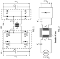
- FIG. 1 shows a schematic diagram of a series-series resonant converter 100 as an isolated power supply for a gate driver.
- a resonant converter is typically used over non-resonant counterparts to reduce the effect of the leakage inductance on the output voltage regulation of the converter.
- a full-bridge inverter 102 is used to generate a high frequency AC signal from the DC voltage (v dc,in ).
- the resonant tank includes capacitors C 1 and C 2 connected in series with the transformer on both the primary and the secondary side.
- a diode bridge rectifier 104 is connected on the secondary side to convert the high frequency AC signal to an isolated DC voltage.
- FIG. 2 shows a schematic diagram of a conventional isolated power supply based on a transformer.
- the series-series compensated topology, as well as the diode bridge rectifier is shown in a simplified version in the figure.
- a conventional transformer having a complete closed magnetic core is used as the isolation structure for the isolated power supply.
- these types of transformers are used for providing electrical insulation.
- the major advantage of using such a structure is that this structure offers a very high magnetizing inductance and low leakage inductance which is preferred in certain applications since the core does not have any air gap and the windings are placed closed to the core. Since these structures offer a low leakage inductance, a non-resonant topology can also be used to drive these transformers.
- the windings may also be made on a PCB based structure.
- this generally increases the leakage inductance of the transformer.
- the insulation needs to be achieved between the windings and the core, which might not always be preferred.
- FIG. 3 is a schematic diagram of a conventional isolated power supply based on a transformer with air gap and insulation.
- the isolated power supply as shown in FIG. 3 is a design variation of that shown in FIG. 2 .
- a small air gap is introduced between the cores, and an insulation layer is provided.
- This structure offers a lower magnetizing inductance as compared to FIG. 2 .
- this design proves to be advantageous when a medium/high voltage isolation is required between the primary side and the secondary side winding.
- the insulation requirement transfers from the winding-to-core to the insulation between the air gap, and it is easier to achieve this insulation.
- FIG. 4 is a schematic diagram of a power supply based on air core with an interlink coil.
- an air core transformer is introduced, which includes the primary winding and the secondary winding, without any magnetic coupling between them.
- the structure does not contain any magnetic material.
- An interlink wire 410 is used to improve the coupling between the primary and the secondary winding structure.
- FIG. 5 illustrates a schematic diagram of an isolated power supply 500 including coupling coils and ferrite cores to improve the coupling between primary and secondary windings, in accordance with an embodiment of the present disclosure.
- each isolated power supply 500 for gate driver includes a primary winding 510 with a magnetic material (e.g., a ferrite core), a secondary winding 520 with a magnetic material (e.g., a ferrite core) and a coupling coil 530, along with additional power electronic converter systems.
- the presence of the magnetic materials between the individual windings helps in increasing the magnetic coupling between primary and secondary windings 510 and 520.
- Coupling coil 530 is added to further improve the magnetic coupling between primary and secondary windings 510 and 520.
- Primary winding 510, secondary winding 520, coupling coil 530, and the magnetic cores are arranged in such a way that it provides an acceptable magnetic coupling, while maintaining a high voltage insulation between primary and secondary windings 510 and 530. This maintains the electric field in the structure to be less than 10 kV/mm. Further, the arrangement is made in such a manner that the capacitance between primary and secondary windings 510 and 520 is low.
- the coupled transformer is connected to a power electronics converter which converts DC to high frequency AC.
- the output side of this coupled transformer is connected to a rectifier which converts the high frequency AC to DC which can be connected to the load.
- inductor Li could be realized as the self-inductance of primary winding 510 of the coupled transformer and inductor L 2 may be realized as the self-inductance of secondary winding 520 of the coupled transformer.
- the coupled transformer is assumed to have a coupling factor k, which may be in range of 0.2-0.5 (loosely coupled).
- Capacitor Ci is connected with primary winding 510 of the coupled transformer and capacitor C 2 is connected with secondary winding 520 of the coupled transformer.
- capacitors are designed in such a way that it compensates for the low coupling factor of the coupled transformer.
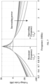
- FIG. 7 illustrates a graphical representation of the gain curve of the series-series resonant converter of FIG. 6 , and the choice for the operating frequency of the converter to achieve a load independent operation.
- the gain of the converter does not change, which gives a load independent output voltage.
- the phase angle of the operating point, as seen by the primary side converter is positive which guarantees soft-switching behavior of the MOSFETs, thus minimizing losses in the converter system.
- a linear voltage regulator may be connected before the output DC port to compensate for small variations in the voltage due to practical considerations.
- FIGs. 8 and 9 show two possible rectifier circuits that may be used in this isolated gate driver system.
- FIG. 8 illustrates a schematic diagram of a rectifier having a diode bridge.
- FIG. 9 illustrates a schematic diagram of a rectifier having a voltage doubler. A capacitor is connected at the output of the diode bridge to filter out any ripples in the voltage. The load is connected across the capacitor.
- FIG. 10 illustrates an isolated gate driver transformer 1000 for a gate driver, in accordance with an embodiment of the present disclosure.
- the isolated gate driver transformer 1000 includes two windings, namely, a primary winding 1010 and a secondary winding 1020. Magnetic cores 1040A and 1040B are inserted between individual windings to increase the inductive coupling between them.
- a coupling coil 1030 is also provided to further increase the inductive coupling between primary and secondary windings 1010 and 1020. The position of coupling coil 1030 determines the inductive coupling.
- input voltage can be applied to primary winding 1010 via primary terminals 1012, while, output voltage can be harvested from secondary winding 1020 via secondary terminals 1022.
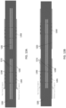
- FIGs. 11A and 11B are sectional views of a PCB-based transformer of FIG. 10 , demonstrating the placement of the coupling coil with respect to the primary and secondary windings.
- FIGs. 11A and 11B show two different options for the placement of coupling coil 1030. It should be noted that in the embodiment the placement of coupling coil 1030 needs to be carried out based on the maximum electric field as well as the inductive coupling. Generally, when the coupling coil is placed between individual coils of the primary/secondary windings, as shown in FIG. 11A , a higher coupling is observed, along with a high electric field. Moving the coupling coil to either the top side or the bottom side of the windings, as shown in FIG. 11B , reduces the maximum electric field, but also reduces the coupling.
- primary winding 1010 includes a top coil layer (made of copper) on a top surface of PCB 1005, and a bottom coil layer (made of copper) on a bottom surface of PCB 1005. Top and bottom coil layers of primary winding 1010 are electrically connected in series.
- secondary winding 1020 includes a top coil layer (made of copper) on a top surface of PCB 1005, and a bottom coil layer (made of copper) on a bottom surface of PCB 1005. Top and bottom coil layers of secondary winding 1020 are electrically connected in series.
- Primary winding 1010 is wound about a primary hole 1001 on PCB 1005, and a first magnetic core can be inserted therein.
- Secondary winding 1020 is wound about a secondary hole 1002 on PCB 1005, and a second magnetic core can be inserted therein. It is appreciated that the first and second magnetic cores may be a single piece or two isolated pieces as shown in FIG. 10 .
- Coupling coil 1030 is embedded in the middle (central layer) of PCB 1005 to form a closed loop that surrounds both primary and secondary holes 1001 and 1002. It is appreciated that multiple loops of coupling coil 1030 could be embedded in PCB 1005 depending on design choices.
- Coupling coil 1030 may be made of any suitable material (e.g., copper or aluminum) that enhances magnetic coupling between primary and secondary windings 1010 and 1020.
- primary winding 1010 includes one or more series-connected coil layers embedded in PCB 1005, and secondary winding 1020 includes one or more series-connected coil layers embedded in PCB 1005.
- Primary winding 1010 is wound about a primary hole 1001 on PCB 1005, and a first magnetic core can be inserted therein.
- Secondary winding 1020 is wound about a secondary hole 1002 on PCB 1005, and a second magnetic core may be inserted therein.
- Coupling coil 1030 may be formed on the top surface of PCB 1005 to form a closed loop that surrounds primary and secondary holes 1001 and 1002. It is appreciated that one or more additional coupling coils can be formed on a bottom surface of PCB 1005 or embedded in PCB 1005 depending on design choices.
- FIG. 12 illustrates an isolated gate driver transformer 1200 for a gate driver having increased coupling between primary and secondary windings 1210 and 1220, in accordance with another embodiment of the present disclosure.
- two coupling coils 1230 are included to the isolation stage to further increase the inductive coupling coefficient between primary and the secondary windings 1210 and 1220.
- FIGs. 13A and 13B are sectional views of a PCB-based transformer of FIG. 12 , demonstrating the placement of the coupling coil with respect to the primary and secondary windings.
- FIGs. 13A and 13B show two different placement options for coupling coils 1230.
- input voltage can be applied to primary winding 1210 via primary terminals 1212, while, output voltage can be harvested from secondary winding 1220 via secondary terminals 1222.
- first and second coupling coils 1230 are respectively formed on top and bottom surfaces of PCB 1205, while primary and secondary windings 1210 and 1220 are disposed in the middle of PCB 1205.
- Primary winding 1210 is wound about a primary hole 1201 on PCB 1205, and a first magnetic core may be inserted therein.
- Secondary winding 1220 is wound about a secondary hole 1202 on PCB 1205, and a second magnetic core may be inserted therein. It is appreciated that the first and second magnetic cores may be a single piece or two isolated pieces as shown in FIG. 12 .
- Coupling coils 1230 are respectively formed on top and bottom surfaces of PCB 1205 to form closed loops that surround both primary and secondary holes 1201 and 1202.
- first and second coupling coils 1230 are disposed in the middle of PCB 1205, while primary and secondary windings 1210 and 1220 are formed on top and bottom surfaces of PCB 1205.
- Coupling coils 1230 form closed loops that surround both primary and secondary holes 1201 and 1202, and are electrically insulated between each other. It is appreciated that variations to the quantity of coupling coils 1230 and the placement thereof can be carried out by one of ordinary skill in the art.
- FIG. 14 illustrates a schematic diagram of a coupled transformer with primary and secondary windings and a coupling coil using copper wires and plastic (or any non-conductive material) bobbins and housing magnetic cores (made of, e.g., ferrite), in accordance with a further embodiment of the present disclosure.
- primary winding 1410 is wound about first bobbin 1450
- secondary wining 1420 is would about second bobbin 1460.
- Each of first and second bobbins 1450 and 1460 includes a magnetic core 1440 inserted therein.
- Coupling coil 1430 forms a closed loop around both primary and secondary windings 1410 and 1420 with magnetic cores 1440 inserted in first and second bobbins 1450 and 1460, on which primary and secondary windings 1410 and 1420 are respectively wound.
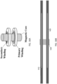
- FIGs. 15A and 15B illustrate a variation of the coupled transformer of FIG. 14 , with the windings and the coupling coil wound about a single magnetic core structure.
- primary and the secondary windings 1510 and 1520 are placed around the same magnetic core 1540.
- the structure may be realized using two different PCBs 1502 and 1504 with one placed on top of the other, with or without a gap between the PCBs.
- coupling coil 1530 is realized using a conductive copper wire placed around the primary winding and the secondary winding to improve the magnetic coupling.
- coupling coil 1530 includes a first semicircular wire 1531 proximate primary winding 1510, a second semicircular wire 1532 proximate secondary winding 1520, and two side wires 1533 connecting the first and second semicircular wires 1531 and 1532, thereby forming a closed loop.
- coupling coil 1530 may not be required, and the required inductive coupling may be established by the ferrite core itself as shown in FIGs. 16A and 16B . Similar to the case in FIGs. 15A and 15B , the design in FIGs. 16A and 16B may be realized using PCB or with plastic (or any non-conductive material) based bobbin structure.
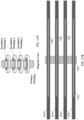
- FIGs. 17A and 17B illustrate another variation of the coupled transformer of FIG. 14 , with a primary winding and multiple secondary windings wound about a single magnetic core structure, without the coupling coil.
- one PCB-based primary winding 1710 and multiple PCB-based secondary windings 1720 are coupled together through a magnetic core 1740.
- Each of PCB-based primary and second windings 1710 and 1720 has a central hole, such that magnetic core 1740 can be inserted therein.
- PCB-based primary and second windings 1710 and 1720 are stacked on top of each other and separated by an equal distance.
- the multiple PCB-based secondary windings 1720 can be electrically connected in series to form a coil of more turns, or electrically separated to harvest electric power independently. In one embodiment, it is appreciated that any suitable quantity of PCB-based primary and second windings 1710 and 1720 can be used in accordance with design choices.
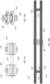
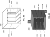
- FIG. 18 illustrates a container 1800 for housing a PCB-based transformer, in accordance with an embodiment of the present disclosure.
- container 1800 includes a bottom plate 1810 and four side plates 1820, so as to form a hollow rectangular cuboid having with an opening.
- Bottom plate 1810 and side plates 1820 may be manufactured as an integrated piece using a suitable additive manufacturing process, such as, 3D printing.
- a plurality of slots 1830 may be formed on opposing side plates 1820 to guide PCB-based windings into and out of container 1800.
- Additional slots 1840 may be formed on bottom plate 1810 to enhance the mechanical stability of the PCB-based windings when inserted in container 1800.
- Slots 1830 and 1840 may be spatially separated with each other by a predetermined distance to ensure that PCB-based windings are properly separated when inserted.
- PCB-based primary and secondary windings can be inserted into or pulled out from container 1800 from different sides of container 1800.
- a first opening is formed on a first side of container 1800 for insertion of the PCB-based primary windings
- a second opening is formed on a second side of container 1800 opposing the first side for insertion of the PCB-based secondary windings.
- FIG. 19 illustrates a container 1900 in which a PCB-based transformer is housed, in accordance with an embodiment of the present disclosure.
- a PCB-based transformer in accordance with an embodiment of the present disclosure.
- four PCB-based windings 1910 are inserted in container 1900. It is appreciated that some of PCB-based windings 1910 can serve as a primary winding, while the other ones of PCB-based windings 1910 can serve as a secondary winding.
- Each of PCB-based windings 1910 includes a central through hole 1912 for a magnetic core 1916 (having a suitable size that fits in container 1900) to penetrate therethrough, as shown in FIG.
- PCB-based windings 1910 can be encapsulated by filling a resin material in container 1900.
- Terminals 1914 of all PCB windings 1910 can be arranged at the same side of container 1900.
- each of terminals 1914 is electrically coupled to an electric wire, leading to the outside of the encapsulant (after terminals 1914 are buried by the encapsulant), so as to be exposed exterior to the encapsulant and allow easy electrical connection after the encapsulation process.
- the present disclosure also provides a method for manufacturing a transformer, which includes the following steps. First, a container having an opening is provided. Then, a plurality of PCB-based windings are inserted in the container through the opening, and each PCB-based winding has one or more terminals such that all the terminals of the PCB-based windings are arranged at a same side of the container. Then, the transformer is encapsulated by filling an encapsulant in the container through the opening, with each PCB-based winding being connected to an electric wire leading exterior to the encapsulant. In an embodiment, prior to inserting the PCB-based windings in the container, the method further includes a step of inserting a magnetic core through a central through hole of each PCB-based winding.
- the method for manufacturing a transformer of one embodiment of the present disclosure includes:
Landscapes
- Engineering & Computer Science (AREA)
- Power Engineering (AREA)
- Microelectronics & Electronic Packaging (AREA)
- Manufacturing & Machinery (AREA)
- Coils Or Transformers For Communication (AREA)
- Coils Of Transformers For General Uses (AREA)
Abstract
Description
- The present disclosure relates to a printed circuit board (PCB) for a power supply. More specifically, the present disclosure relates to a power transformer for the power supply and a manufacturing method thereof.
- The advancement of wide bandgap semiconductor devices such as Silicon Carbide metal-oxide-field-effect transistors (SiC MOSFETs), Silicon Carbide insulated-gate-bipolar-transistors (SiC IGBTs) and Gallium Nitride Field Effect Transistors (GaN FETs) requires certain advanced design considerations from the perspective of driving the power semiconductor devices. Nowadays, power semiconductor devices are available for blocking voltages of more than 15 kV and an isolated power supply for the gate driver is required for driving these devices. Due to the high switching speed (dv/dt) and the high voltage isolation requirement for the medium voltage devices, it is necessary to have an isolated power supply for the gate driver which can handle the high voltage while having a low parasitic capacitance across the isolation barrier.
- For the isolated power supply, the isolation is typically obtained by a conventional transformer using a magnetic core. This solution has been widely used in the industry as well as the academia for both silicon and silicon carbide devices, especially when the blocking voltage of each device is less than 3.3 kV This solution is also used for silicon devices with higher blocking voltage (~6.5 kV). However, for medium voltage SiC power devices, owing to its fast-switching transients, special considerations are taken while designing this isolated power supply. Along with the high isolation capability of the isolated power supply, a small parasitic capacitance is imperative for driving fast switching SiC devices.
-
FIG. 1 shows a conventional isolated power supply with a series-series resonant converter. However, both resonant and non-resonant topologies can be used to form the primary side of the isolated power supply. Similarly, the diodes in the secondary side can also be replaced by active devices under certain conditions. Using this structure for driving medium voltage SiC devices requires certain changes in the structure of the conventional transformer core, to account for the high voltage blocking capacity and the requirement of low parasitic capacitance. - The following references disclose conventional transformer structures that provide the required MV (medium voltage) isolation for the gate drivers, and have been demonstrated for MV SiC power devices. Nevertheless, while the techniques disclosed in the references can achieve a high isolation along with a reduction in parasitic capacitance, they result in a high device volume and thus are difficult to manufacture.
- [Ref. 1] A. Kadavelugu and S. Bhattacharya, "Design considerations and development of gate driver for 15 kV SiC IGBT," 2014 IEEE Applied Power Electronics Conference and Exposition - APEC 2014, 2014, pp. 1494-1501, doi: 10.1109/APEC.2014.6803505 ("Kadavelugu").
- [Ref. 2] A. Anurag, S. Acharya, Y. Prabowo, G. Gohil and S. Bhattacharya, "Design Considerations and Development of an Innovative Gate Driver for Medium-Voltage Power Devices With High dv/dt," in IEEE Transactions on Power Electronics, vol. 34, no. 6, pp. 5256-5267, June 2019, doi: 10.1109/TPEL.2018.2870084 ("Anurag").
- [Ref. 3] L. Zhang et al., "Design Considerations for High-Voltage Insulated Gate Drive Power Supply for 10-kV SiC MOSFET Applied in Medium-Voltage Converter," in IEEE Transactions on Industrial Electronics, vol. 68, no. 7, pp. 5712-5724, July 2021, doi: 10.1109/TIE.2020.3000131 ("Zhang").
- In Kadavelugu's design, a toroidal magnetic core is used with copper wires wound across the same with Kapton tape in between to achieve the required insulation. This, however, gives a high parasitic capacitance and the Kapton tape does not provide a reliable insulation for the MV isolation. In Anurag's solution and Zhang's solution, the copper wire used in Kadavelugu's solution was replaced with PCB (printed circuit board) winding and the toroidal shaped core is changed to two connected C-cores. Zhang enclosed the whole power supply in a potting material. This increases the reliability of the isolated power supply, but due to the presence of two C-cores leads to difficulty in manufacturing.
- Another solution is proposed in an article titled "Highly Compact Isolated Gate Driver With Ultrafast Overcurrent Protection for 10 kV SiC MOSFETs" by Rothmund et al., published in CPSS Transactions on Power Electronics and Applications, vol. 3, no. 4, pp. 278-291, Dec. 2018 ("Rothmund") [Ref. 4]. Rothmund achieves the required MV isolation of the transformer by separating the cores and placing an air gap between them. The winding is realized using litz wire and the entire isolated power supply was enclosed in a potting material.
- An article titled "Current-Transformer Based Gate-Drive Power Supply with Reinforced Isolation", by Hu et al. published in 2018 IEEE Energy Conversion Congress and Exposition (ECCE), 2018 [Ref. 5], takes a different approach and uses a current transformer based gate driver power supply. The required MV isolation is achieved by using a MV insulated wire on the primary side of the isolated power supply. A similar approach is also reported in "A galvanically isolated gate driver with low coupling capacitance for medium voltage SiC MOSFETs" by Gottschlich et al. in 2016 18th European Conference on Power Electronics and Applications (EPE'16 ECCE Europe).
- In another article titled "Design of Gate Drive Power Supply with Air Core Transformer for High dv/dt Switching", by Mainali et al. published in 2018 IEEE Energy Conversion Congress and Exposition (ECCE), 2018 [Ref. 6], the authors have demonstrated the operation of an air core transformer with low coupling capacitance. The design does not contain any magnetic material and uses an interlink coil to increase the coupling between the primary and secondary side winding. This concept is also patented in a patent titled "Gate Driver" (
Wang R. et al., "Gate Driver", US Patent No. 10,809,326 B2, issued Oct. 20, 2020 - While the existing methods are capable of achieving the required MV isolation along with having a low parasitic capacitance, there is a need to provide a more comprehensive solution which provides good performance and can be manufactured easily.
- In one aspect, the present disclosure provides a power transformer including: a primary winding and a secondary winding; a primary magnetic core wound by the primary winding; a secondary magnetic core wound by the secondary winding; and an electrically conductive coupling coil wound about the primary and secondary magnetic cores.
- In one embodiment, the primary winding includes a first top coil and a first bottom coil electrically connected to the first top coil, and wherein the secondary winding includes a second top coil and a bottom coil electrically connected to the second top coil.
- In one embodiment, the coupling coil is a closed loop disposed between the first and second top coils and the first and second bottom coils.
- In one embodiment, the power transformer further includes a printed circuit board (PCB) having a first hole and a second hole, wherein the first and second top coils are disposed on a top surface of the PCB, wherein the first and second bottom coils are disposed on a bottom surface of the PCB, and wherein the coupling coil is embedded in a central layer of the PCB.
- In one embodiment, the primary magnetic core is inserted in the first hole and the secondary magnetic core is inserted in the second hole.
- In one embodiment, the power transformer further includes a printed circuit board (PCB) having a first hole and a second hole, wherein the primary and secondary windings are embedded in a central layer of the PCB, and wherein the coupling coil is disposed on a surface of the PCB.
- In one embodiment, the coupling coil includes a first closed loop and a second closed loop.
- In one embodiment, the primary and secondary windings are disposed between the first and second closed loops.
- In one embodiment, the power transformer further includes a printed circuit board (PCB) having a first hole and a second hole, wherein the primary and secondary windings are embedded in a central layer of the PCB, wherein the first closed loop is disposed on a top surface of the PCB, and wherein the second closed loop is disposed on a bottom surface of the PCB.
- In one embodiment, the primary magnetic core is inserted in the first hole and the secondary magnetic core is inserted in the second hole.
- In another aspect, the present disclosure provides a printed circuit board (PCB), including: a primary winding wound about a first hole of the PCB; a secondary winding wound about a second hole of the PCB; and a coupling coil forming a closed loop surrounding the first and second holes of the PCB.
- In one embodiment, the coupling coil is embedded in a central layer of the PCB.
- In one embodiment, the coupling coil includes a plurality of conductive loops that are electrically insulated from each other.
- In one embodiment, the primary winding includes a top layer on a top surface of the PCB and a bottom layer on a bottom surface of the PCB, the top and bottom layers of the primary winding being electrically connected.
- In one embodiment, the secondary winding includes a top layer on a top surface of the PCB and a bottom layer on a bottom surface of the PCB, the top and bottom layers of the secondary winding being electrically connected.
- In one embodiment, the primary and secondary windings are embedded in a central layer of the PCB.
- In one embodiment, the coupling coil is disposed on a top surface of the PCB
- In one embodiment, the coupling coil includes a first coupling coil and a second coupling coil, wherein the first coupling coil is disposed on a top surface of the PCB and the second coupling coil is disposed on a bottom surface of the PCB.
- In one embodiment, the PCB further includes primary terminals to receive an input voltage applied to the primary winding.
- In one embodiment, the PCB further includes secondary terminals to provide an output voltage induced by the secondary winding.
- In another aspect, the present disclosure provides a method for manufacturing a transformer, including: providing a container having an opening; inserting a plurality of PCB-based windings in the container through the opening, each of the plurality of PCB-based windings having one or more terminals, such that all the terminals of the plurality of PCB-based windings are arranged at a same side of the container; and encapsulating the transformer by filling an encapsulant in the container through the opening, with each of the terminals of the plurality of PCB-based windings being connected to an electric wire leading exterior to the encapsulant.
- In one embodiment, the method for manufacturing a transformer further includes: prior to inserting the plurality of PCB-based windings in the container, inserting a magnetic core through a central through hole of each of the plurality of PCB-based windings.
-
-
FIG. 1 illustrates a schematic diagram of a series-series resonant converter as an isolated power supply for a gate driver. -
FIG. 2 illustrates a schematic diagram of a conventional isolated power supply based on a transformer. -
FIG. 3 illustrates a schematic diagram of a conventional isolated power supply based on a transformer with air gap and insulation. -
FIG. 4 illustrates a schematic diagram of a power supply based on air core with an interlink coil. -
FIG. 5 illustrates a schematic diagram of an isolated power supply including coupling coils and ferrite cores to improve the coupling between primary and secondary winding, in accordance with an embodiment of the present disclosure. -
FIG. 6 illustrates the schematic diagram of the circuit model for a series-series resonant converter, with a small coupling coefficient, in accordance with an embodiment of the present disclosure. -
FIG. 7 illustrates a graphical representation of the gain curve of the series-series resonant converter ofFIG. 6 , and the choice for the operating frequency of the converter to achieve a load independent operation. -
FIG. 8 illustrates a schematic diagram of a rectifier having a diode bridge. -
FIG. 9 illustrates a schematic diagram of a rectifier having a voltage doubler. -
FIG. 10 illustrates an isolated gate driver transformer for a gate driver, in accordance with an embodiment of the present disclosure. -
FIGs. 11A and 11B are sectional views of a PCB-based transformer ofFIG. 10 , demonstrating the placement of the coupling coil with respect to the primary and secondary windings. -
FIG. 12 illustrates an isolated gate driver transformer for a gate driver having increased coupling between primary and secondary windings, in accordance with another embodiment of the present disclosure. -
FIGs. 13A and 13B are sectional views of a PCB-based transformer ofFIG. 12 , demonstrating the placement of the coupling coil with respect to the primary and secondary windings. -
FIG. 14 illustrates a schematic diagram of a coupled transformer with primary and secondary windings and a coupling coil using copper wires and plastic (or any non-conductive material) bobbins housing magnetic cores (made of, e.g., ferrite), in accordance with a further embodiment of the present disclosure. -
FIGs. 15A and 15B illustrate a variation of the coupled transformer ofFIG. 14 , with the windings and the coupling coil wound about a single magnetic core structure. -
FIGs. 16A and 16B illustrate a variation of the coupled transformer ofFIG. 14 , with the windings wound about a single magnetic core structure, without the coupling coil. -
FIGs. 17A and 17B illustrate another variation of the coupled transformer ofFIG. 14 , with a primary winding and multiple secondary windings wound about a single magnetic core structure, without the coupling coil. -
FIG. 18 illustrates a container for housing a PCB-based transformer, in accordance with an embodiment of the present disclosure. -
FIG. 19 illustrates a container in which a PCB-based transformer is housed, in accordance with an embodiment of the present disclosure. - The present disclosure will now be described more specifically with reference to the accompanying drawings. It is to be noted that the following detailed descriptions are presented herein for purpose of illustration and description only. It is not intended to be exhaustive or to be limited to the precise form disclosed.
- One embodiment of the present disclosure is aimed at an isolated power supply for a gate driver using a coupled transformer capable of being reliably utilized in medium voltage converter systems. The isolated power supply includes a coupled transformer and a resonant converter. The coupled transformer is coupled using two magnetic cores and coupling coils. In the embodiment, the structure helps in achieving a low parasitic capacitance between the primary and secondary windings, while maintaining a high voltage insulation, which is necessary for operating medium voltage converter systems. The low parasitic capacitance between the primary and the secondary winding reduces the effect of the fast-switching transients (dv/dt) of the device.
-
FIG. 1 shows a schematic diagram of a series-seriesresonant converter 100 as an isolated power supply for a gate driver. A resonant converter is typically used over non-resonant counterparts to reduce the effect of the leakage inductance on the output voltage regulation of the converter. As shown inFIG. 1 , a full-bridge inverter 102 is used to generate a high frequency AC signal from the DC voltage (vdc,in). The resonant tank includes capacitors C1 and C2 connected in series with the transformer on both the primary and the secondary side. Adiode bridge rectifier 104 is connected on the secondary side to convert the high frequency AC signal to an isolated DC voltage. -
FIG. 2 shows a schematic diagram of a conventional isolated power supply based on a transformer. The series-series compensated topology, as well as the diode bridge rectifier is shown in a simplified version in the figure. As seen, a conventional transformer having a complete closed magnetic core is used as the isolation structure for the isolated power supply. Conventionally, these types of transformers are used for providing electrical insulation. The major advantage of using such a structure is that this structure offers a very high magnetizing inductance and low leakage inductance which is preferred in certain applications since the core does not have any air gap and the windings are placed closed to the core. Since these structures offer a low leakage inductance, a non-resonant topology can also be used to drive these transformers. With some variations, the windings may also be made on a PCB based structure. However, this generally increases the leakage inductance of the transformer. In case a medium/high voltage is required between the primary and the secondary side, the insulation needs to be achieved between the windings and the core, which might not always be preferred. -
FIG. 3 is a schematic diagram of a conventional isolated power supply based on a transformer with air gap and insulation. The isolated power supply as shown inFIG. 3 is a design variation of that shown inFIG. 2 . As shown inFIG. 3 , a small air gap is introduced between the cores, and an insulation layer is provided. This structure offers a lower magnetizing inductance as compared toFIG. 2 . However, this design proves to be advantageous when a medium/high voltage isolation is required between the primary side and the secondary side winding. The insulation requirement transfers from the winding-to-core to the insulation between the air gap, and it is easier to achieve this insulation. -
FIG. 4 is a schematic diagram of a power supply based on air core with an interlink coil. As shown inFIG. 4 , an air core transformer is introduced, which includes the primary winding and the secondary winding, without any magnetic coupling between them. The structure does not contain any magnetic material. Aninterlink wire 410 is used to improve the coupling between the primary and the secondary winding structure. -
FIG. 5 illustrates a schematic diagram of anisolated power supply 500 including coupling coils and ferrite cores to improve the coupling between primary and secondary windings, in accordance with an embodiment of the present disclosure. As depicted inFIG. 5 , eachisolated power supply 500 for gate driver includes a primary winding 510 with a magnetic material (e.g., a ferrite core), a secondary winding 520 with a magnetic material (e.g., a ferrite core) and acoupling coil 530, along with additional power electronic converter systems. The presence of the magnetic materials between the individual windings helps in increasing the magnetic coupling between primary andsecondary windings 510 and 520.Coupling coil 530 is added to further improve the magnetic coupling between primary andsecondary windings 510 and 520. Primary winding 510, secondary winding 520,coupling coil 530, and the magnetic cores are arranged in such a way that it provides an acceptable magnetic coupling, while maintaining a high voltage insulation between primary andsecondary windings 510 and 530. This maintains the electric field in the structure to be less than 10 kV/mm. Further, the arrangement is made in such a manner that the capacitance between primary andsecondary windings 510 and 520 is low. As shown, the coupled transformer is connected to a power electronics converter which converts DC to high frequency AC. The output side of this coupled transformer is connected to a rectifier which converts the high frequency AC to DC which can be connected to the load. - When the coupled transformer has a low inductive coupling coefficient, as in this embodiment, a resonant converter is necessary to achieve voltage regulation on the output. A series-series resonant converter as shown in
FIG. 6 could be used to achieve the required voltage regulation. Here, inductor Li could be realized as the self-inductance of primary winding 510 of the coupled transformer and inductor L2 may be realized as the self-inductance of secondary winding 520 of the coupled transformer. The coupled transformer is assumed to have a coupling factor k, which may be in range of 0.2-0.5 (loosely coupled). Capacitor Ci is connected with primary winding 510 of the coupled transformer and capacitor C2 is connected with secondary winding 520 of the coupled transformer. These capacitors are designed in such a way that it compensates for the low coupling factor of the coupled transformer. The design stems from the fact that the resonant converter is operated at a frequency which gives the best voltage regulation. This is achieved by designing the capacitance and operating frequency according to:
-
FIG. 7 illustrates a graphical representation of the gain curve of the series-series resonant converter ofFIG. 6 , and the choice for the operating frequency of the converter to achieve a load independent operation. As shown inFIG. 7 , at the operating frequency f op, the gain of the converter does not change, which gives a load independent output voltage. Further, because the operation is carried out slightly above the resonant frequency f res, the phase angle of the operating point, as seen by the primary side converter, is positive which guarantees soft-switching behavior of the MOSFETs, thus minimizing losses in the converter system. A linear voltage regulator may be connected before the output DC port to compensate for small variations in the voltage due to practical considerations. - In all isolated power supplies, a rectifier is included to convert the high frequency AC that is seen at the secondary winding of the transformer.
FIGs. 8 and 9 show two possible rectifier circuits that may be used in this isolated gate driver system.FIG. 8 illustrates a schematic diagram of a rectifier having a diode bridge.FIG. 9 illustrates a schematic diagram of a rectifier having a voltage doubler. A capacitor is connected at the output of the diode bridge to filter out any ripples in the voltage. The load is connected across the capacitor. -
FIG. 10 illustrates an isolatedgate driver transformer 1000 for a gate driver, in accordance with an embodiment of the present disclosure. The isolatedgate driver transformer 1000 includes two windings, namely, a primary winding 1010 and a secondary winding 1020.Magnetic cores coupling coil 1030 is also provided to further increase the inductive coupling between primary andsecondary windings coupling coil 1030 determines the inductive coupling. In operation, input voltage can be applied to primary winding 1010 viaprimary terminals 1012, while, output voltage can be harvested from secondary winding 1020 viasecondary terminals 1022. -
FIGs. 11A and 11B are sectional views of a PCB-based transformer ofFIG. 10 , demonstrating the placement of the coupling coil with respect to the primary and secondary windings.FIGs. 11A and 11B show two different options for the placement ofcoupling coil 1030. It should be noted that in the embodiment the placement ofcoupling coil 1030 needs to be carried out based on the maximum electric field as well as the inductive coupling. Generally, when the coupling coil is placed between individual coils of the primary/secondary windings, as shown inFIG. 11A , a higher coupling is observed, along with a high electric field. Moving the coupling coil to either the top side or the bottom side of the windings, as shown inFIG. 11B , reduces the maximum electric field, but also reduces the coupling. - As shown in
FIG. 11A , primary winding 1010 includes a top coil layer (made of copper) on a top surface ofPCB 1005, and a bottom coil layer (made of copper) on a bottom surface ofPCB 1005. Top and bottom coil layers of primary winding 1010 are electrically connected in series. Likewise, secondary winding 1020 includes a top coil layer (made of copper) on a top surface ofPCB 1005, and a bottom coil layer (made of copper) on a bottom surface ofPCB 1005. Top and bottom coil layers of secondary winding 1020 are electrically connected in series. Primary winding 1010 is wound about aprimary hole 1001 onPCB 1005, and a first magnetic core can be inserted therein. Secondary winding 1020 is wound about asecondary hole 1002 onPCB 1005, and a second magnetic core can be inserted therein. It is appreciated that the first and second magnetic cores may be a single piece or two isolated pieces as shown inFIG. 10 .Coupling coil 1030 is embedded in the middle (central layer) ofPCB 1005 to form a closed loop that surrounds both primary andsecondary holes coupling coil 1030 could be embedded inPCB 1005 depending on design choices.Coupling coil 1030 may be made of any suitable material (e.g., copper or aluminum) that enhances magnetic coupling between primary andsecondary windings - Alternatively, as shown in
FIG. 11B , primary winding 1010 includes one or more series-connected coil layers embedded inPCB 1005, and secondary winding 1020 includes one or more series-connected coil layers embedded inPCB 1005. Primary winding 1010 is wound about aprimary hole 1001 onPCB 1005, and a first magnetic core can be inserted therein. Secondary winding 1020 is wound about asecondary hole 1002 onPCB 1005, and a second magnetic core may be inserted therein.Coupling coil 1030 may be formed on the top surface ofPCB 1005 to form a closed loop that surrounds primary andsecondary holes PCB 1005 or embedded inPCB 1005 depending on design choices. -
FIG. 12 illustrates an isolatedgate driver transformer 1200 for a gate driver having increased coupling between primary andsecondary windings FIG. 12 , twocoupling coils 1230 are included to the isolation stage to further increase the inductive coupling coefficient between primary and thesecondary windings FIGs. 13A and 13B are sectional views of a PCB-based transformer ofFIG. 12 , demonstrating the placement of the coupling coil with respect to the primary and secondary windings.FIGs. 13A and 13B show two different placement options forcoupling coils 1230. In operation, input voltage can be applied to primary winding 1210 viaprimary terminals 1212, while, output voltage can be harvested from secondary winding 1220 viasecondary terminals 1222. - As shown in
FIG. 13A , first andsecond coupling coils 1230 are respectively formed on top and bottom surfaces ofPCB 1205, while primary andsecondary windings PCB 1205. Primary winding 1210 is wound about aprimary hole 1201 onPCB 1205, and a first magnetic core may be inserted therein. Secondary winding 1220 is wound about asecondary hole 1202 onPCB 1205, and a second magnetic core may be inserted therein. It is appreciated that the first and second magnetic cores may be a single piece or two isolated pieces as shown inFIG. 12 . Coupling coils 1230 are respectively formed on top and bottom surfaces ofPCB 1205 to form closed loops that surround both primary andsecondary holes - In contrast, as shown in
FIG. 13B , first andsecond coupling coils 1230 are disposed in the middle ofPCB 1205, while primary andsecondary windings PCB 1205. Coupling coils 1230 form closed loops that surround both primary andsecondary holes coupling coils 1230 and the placement thereof can be carried out by one of ordinary skill in the art. -
FIG. 14 illustrates a schematic diagram of a coupled transformer with primary and secondary windings and a coupling coil using copper wires and plastic (or any non-conductive material) bobbins and housing magnetic cores (made of, e.g., ferrite), in accordance with a further embodiment of the present disclosure. As shown inFIG. 14 , primary winding 1410 is wound aboutfirst bobbin 1450, whilesecondary wining 1420 is would aboutsecond bobbin 1460. Each of first andsecond bobbins magnetic core 1440 inserted therein.Coupling coil 1430 forms a closed loop around both primary andsecondary windings magnetic cores 1440 inserted in first andsecond bobbins secondary windings -
FIGs. 15A and 15B illustrate a variation of the coupled transformer ofFIG. 14 , with the windings and the coupling coil wound about a single magnetic core structure. As shown, primary and thesecondary windings magnetic core 1540. The structure may be realized using twodifferent PCBs FIGs. 15A and 15B ,coupling coil 1530 is realized using a conductive copper wire placed around the primary winding and the secondary winding to improve the magnetic coupling. In one embodiment,coupling coil 1530 includes a firstsemicircular wire 1531 proximate primary winding 1510, a secondsemicircular wire 1532 proximate secondary winding 1520, and twoside wires 1533 connecting the first and secondsemicircular wires coupling coil 1530 may not be required, and the required inductive coupling may be established by the ferrite core itself as shown inFIGs. 16A and 16B . Similar to the case inFIGs. 15A and 15B , the design inFIGs. 16A and 16B may be realized using PCB or with plastic (or any non-conductive material) based bobbin structure. -
FIGs. 17A and 17B illustrate another variation of the coupled transformer ofFIG. 14 , with a primary winding and multiple secondary windings wound about a single magnetic core structure, without the coupling coil. As shown inFIGs. 17A and 17B , one PCB-based primary winding 1710 and multiple PCB-basedsecondary windings 1720 are coupled together through amagnetic core 1740. Each of PCB-based primary andsecond windings magnetic core 1740 can be inserted therein. In one embodiment, PCB-based primary andsecond windings secondary windings 1720 can be electrically connected in series to form a coil of more turns, or electrically separated to harvest electric power independently. In one embodiment, it is appreciated that any suitable quantity of PCB-based primary andsecond windings -
FIG. 18 illustrates acontainer 1800 for housing a PCB-based transformer, in accordance with an embodiment of the present disclosure. As shown inFIG. 18 ,container 1800 includes abottom plate 1810 and fourside plates 1820, so as to form a hollow rectangular cuboid having with an opening.Bottom plate 1810 andside plates 1820 may be manufactured as an integrated piece using a suitable additive manufacturing process, such as, 3D printing. A plurality ofslots 1830 may be formed on opposingside plates 1820 to guide PCB-based windings into and out ofcontainer 1800.Additional slots 1840 may be formed onbottom plate 1810 to enhance the mechanical stability of the PCB-based windings when inserted incontainer 1800.Slots - It is appreciated that, in an alternative embodiment, PCB-based primary and secondary windings can be inserted into or pulled out from
container 1800 from different sides ofcontainer 1800. In this embodiment, a first opening is formed on a first side ofcontainer 1800 for insertion of the PCB-based primary windings, while a second opening is formed on a second side ofcontainer 1800 opposing the first side for insertion of the PCB-based secondary windings. -
FIG. 19 illustrates acontainer 1900 in which a PCB-based transformer is housed, in accordance with an embodiment of the present disclosure. As shown inFIG. 19 , in this embodiment, four PCB-basedwindings 1910 are inserted incontainer 1900. It is appreciated that some of PCB-basedwindings 1910 can serve as a primary winding, while the other ones of PCB-basedwindings 1910 can serve as a secondary winding. Each of PCB-basedwindings 1910 includes a central throughhole 1912 for a magnetic core 1916 (having a suitable size that fits in container 1900) to penetrate therethrough, as shown inFIG. 17A , and twoterminals 1914 for electrically coupling PCB-basedwindings 1910 to other circuits, e.g., a rectifier, a power source, a load, etc. In one embodiment, the entire structure can be potted using an encapsulant of relatively high dielectric strength. For example, PCB-basedwindings 1910 can be encapsulated by filling a resin material incontainer 1900.Terminals 1914 of allPCB windings 1910 can be arranged at the same side ofcontainer 1900. In one embodiment, each ofterminals 1914 is electrically coupled to an electric wire, leading to the outside of the encapsulant (afterterminals 1914 are buried by the encapsulant), so as to be exposed exterior to the encapsulant and allow easy electrical connection after the encapsulation process. - In addition, the present disclosure also provides a method for manufacturing a transformer, which includes the following steps. First, a container having an opening is provided. Then, a plurality of PCB-based windings are inserted in the container through the opening, and each PCB-based winding has one or more terminals such that all the terminals of the PCB-based windings are arranged at a same side of the container. Then, the transformer is encapsulated by filling an encapsulant in the container through the opening, with each PCB-based winding being connected to an electric wire leading exterior to the encapsulant. In an embodiment, prior to inserting the PCB-based windings in the container, the method further includes a step of inserting a magnetic core through a central through hole of each PCB-based winding.
- As shown in
FIG. 18 and FIG. 19 , the method for manufacturing a transformer of one embodiment of the present disclosure includes: - providing
container 1900 having an opening; - inserting a plurality of PCB-based
windings 1910 in thecontainer 1900 through the opening, wherein one or more of the PCB-basedwindings 1910 having one ormore terminals 1914, such that theterminals 1914 of the PCB-basedwindings 1910 may be arranged at a same side of thecontainer 1900; and - encapsulating the transformer by filling an encapsulant in the
container 1900 through the opening, with each of theterminals 1914 of the PCB-basedwindings 1910 being connected to an electric wire leading exterior to the encapsulant. In one embodiment, the method further includes a step of inserting a magnetic core through a central through hole of the PCB-based winding before the step of inserting the PCB-basedwindings 1910 in thecontainer 1900. - For the purposes of describing and defining the present disclosure, it is noted that terms of degree (e.g., "substantially," "slightly," "about," "comparable," etc.) may be utilized herein to represent the inherent degree of uncertainty that may be attributed to any quantitative comparison, value, measurement, or other representation. Such terms of degree may also be utilized herein to represent the degree by which a quantitative representation may vary from a stated reference (e.g., about 10% or less) without resulting in a change in the basic function of the subject matter at issue. Unless otherwise stated herein, any numerical value appearing in the present disclosure are deemed modified by a term of degree (e.g., "about"), thereby reflecting its intrinsic uncertainty.
Claims (19)
- A power transformer (1000), characterized by comprising:a primary winding (1010) and a secondary winding (1020);a primary magnetic core (1040A) wound by the primary winding (1010);a secondary magnetic core (1040B) wound by the secondary winding (1020); andan electrically conductive coupling coil (1030) wound about the primary and secondary magnetic cores (1040A, 1040B).
- The power transformer (1000 - FIG. 11A) of claim 1, wherein the primary winding (1010) comprises a first top coil and a first bottom coil electrically connected to the first top coil, and wherein the secondary winding (1020) comprises a second top coil and a bottom coil electrically connected to the second top coil.
- The power transformer (1000) of claim 1 or 2, wherein the coupling coil (1030) is a closed loop disposed between the first and second top coils and the first and second bottom coils.
- The power transformer (1000) of according to any one of the above claims, further comprising a printed circuit board (PCB) (1005) having a first hole (1001) and a second hole (1002), wherein the first top coil of the primary winding (1010) and the second top coil of the secondary winding (1020) are disposed on a top surface of the PCB (1005), wherein the first bottom coil of the primary winding (1010) and the second bottom coil of the secondary winding (1020) are disposed on a bottom surface of the PCB (1005), and wherein the coupling coil (1030) is embedded in the PCB (1005).
- The power transformer (1000 - FIG. 11B) of claim 1, further comprising a printed circuit board (PCB) (1005) having a first hole (1001) and a second hole (1002), wherein the primary and secondary windings (1010, 1020) are embedded in the PCB (1005), and wherein the coupling coil (1030) is disposed on a surface of the PCB (1005).
- The power transformer (1200) of claim 1, wherein the coupling coil (1230) comprises a first closed loop and a second closed loop.
- The power transformer (1200 - FIG. 13A) of claim 6, wherein the primary and secondary windings (1210, 1220) are disposed between the first and second closed loops of the coupling coil (1230).
- The power transformer (1200) of claim 6 or 7, further comprising a printed circuit board (PCB) (1205) having a first hole (1201) and a second hole (1202), wherein the primary and secondary windings (1210, 1220) are embedded in the PCB (1205), wherein the first closed loop of the coupling coil (1230) is disposed on a top surface of the PCB (1205), and wherein the second closed loop of the coupling coil (1230) is disposed on a bottom surface of the PCB (1205).
- The power transformer according to any one of the above claims, wherein the primary magnetic core (1040A, 1240) is inserted in the first hole (1001, 1201), and the secondary magnetic core (1040B, 1240) is inserted in the second hole (1002, 1202).
- A printed circuit board (PCB) (1005), characterized by comprising:a primary winding (1010) wound about a first hole (1001) of the PCB (1005);a secondary winding (1020) wound about a second hole (1002) of the PCB (1005); anda coupling coil (1030) forming a closed loop that surrounds the first and second holes (1001, 1002) of the PCB (1005).
- The PCB (1005) of claim 10, wherein the coupling coil (1030) is embedded in the PCB (1005).
- The PCB (1205) of claim 10 or 11, wherein the coupling coil (1230) comprises a plurality of conductive loops that are electrically insulated from each other.
- The PCB (1005 - FIG. 11A) according to any one of claims 10 to 12, wherein the primary winding (1010) comprises a top layer on a top surface of the PCB (1005) and a bottom layer on a bottom surface of the PCB (1005), the top and bottom layers of the primary winding (1010) being electrically connected; and/or
wherein the secondary winding (1020) comprises a top layer on a top surface of the PCB (1005) and a bottom layer on a bottom surface of the PCB (1005), the top and bottom layers of the secondary winding (1020) being electrically connected. - The PCB (1005 - FIG. 11B) of claim 10, wherein the primary and secondary windings (1010, 1020) are embedded in the PCB (1005).
- The PCB (1005 - FIG. 11B) of claim 10, wherein the coupling coil (1030) is disposed on a top surface of the PCB (1005).
- The PCB (1205 - FIG. 13A) of claim 10, wherein the coupling coil (1230) comprises a first coupling coil and a second coupling coil, wherein the first coupling coil is disposed on a top surface of the PCB (1205) and the second coupling coil is disposed on a bottom surface of the PCB (1205).
- The PCB (1205) according to any of claims 10 to 16, further comprising at least one of primary terminals (1212) to receive an input voltage applied to the primary winding (1210) and secondary terminals (1222) to provide an output voltage induced by the secondary winding (1220).
- A method for manufacturing the transformer according to any of the previous claims, characterized by comprising:providing a container (1900) having an opening;inserting a plurality of PCB-based windings (1910) in the container (1900) through the opening, each of the plurality of PCB-based windings (1910) having one or more terminals (1914), such that all the terminals (1914) of the plurality of PCB-based windings (1910) are arranged at a same side of the container (1900); andfilling an encapsulant in the container (1900) through the opening, with each of the terminals (1914) of the plurality of PCB-based windings (1910) being connected to an electric wire leading exterior to the encapsulant.
- The method of claim 18, further comprising:
prior to inserting the plurality of PCB-based windings (1910) in the container (1900), inserting a magnetic core (1916) through a central through hole (1912) of each of the plurality of PCB-based windings (1910).
Applications Claiming Priority (1)
| Application Number | Priority Date | Filing Date | Title |
|---|---|---|---|
| US18/049,491 US20240186054A1 (en) | 2022-10-25 | 2022-10-25 | Isolated power supply for gate driver |
Publications (1)
| Publication Number | Publication Date |
|---|---|
| EP4362051A1 true EP4362051A1 (en) | 2024-05-01 |
Family
ID=88417496
Family Applications (1)
| Application Number | Title | Priority Date | Filing Date |
|---|---|---|---|
| EP23204030.3A Pending EP4362051A1 (en) | 2022-10-25 | 2023-10-17 | Printed circuit board, power transformer, and manufacturing method thereof |
Country Status (4)
| Country | Link |
|---|---|
| US (1) | US20240186054A1 (en) |
| EP (1) | EP4362051A1 (en) |
| CN (1) | CN118553519A (en) |
| TW (1) | TWI894659B (en) |
Citations (4)
| Publication number | Priority date | Publication date | Assignee | Title |
|---|---|---|---|---|
| EP1536436A1 (en) * | 2002-06-26 | 2005-06-01 | Premo, S.A. | Method of producing planar transformers and planar transformer thus produced |
| EP2144070A1 (en) * | 2008-07-11 | 2010-01-13 | Liaisons Electroniques-Mecaniques Lem S.A. | Sensor for high voltage environment |
| US20150332838A1 (en) * | 2012-11-16 | 2015-11-19 | Phoenix Contact Gmbh & Co.Kg | Planar Transformer |
| US10809326B2 (en) | 2018-01-29 | 2020-10-20 | GE Precision Healthcare LLC | Gate driver |
Family Cites Families (8)
| Publication number | Priority date | Publication date | Assignee | Title |
|---|---|---|---|---|
| US4425511A (en) * | 1981-02-09 | 1984-01-10 | Amnon Brosh | Planar coil apparatus employing a stationary and a movable board |
| US8593244B2 (en) * | 2008-09-18 | 2013-11-26 | The Boeing Company | Control of leakage inductance |
| DE102010049668A1 (en) * | 2010-10-26 | 2012-04-26 | Minebea Co., Ltd. | transformer |
| US8971072B2 (en) * | 2011-12-30 | 2015-03-03 | Bedrock Automation Platforms Inc. | Electromagnetic connector for an industrial control system |
| EP3048618B1 (en) * | 2015-01-20 | 2019-05-29 | Nexperia B.V. | Common mode choke |
| TWI630628B (en) * | 2017-10-19 | 2018-07-21 | 光壽科技有限公司 | Capacitive resistance voltage conversion device |
| CN109712785A (en) * | 2017-10-26 | 2019-05-03 | 通用电气公司 | Potential device, switch driving circuit and pulse power system is isolated |
| US11916490B2 (en) * | 2021-02-10 | 2024-02-27 | Innoscience (Suzhou) Technology Co., Ltd. | Multi-functional PCB for assembling GaN-based power converter |
-
2022
- 2022-10-25 US US18/049,491 patent/US20240186054A1/en active Pending
-
2023
- 2023-10-17 EP EP23204030.3A patent/EP4362051A1/en active Pending
- 2023-10-20 CN CN202311368438.0A patent/CN118553519A/en active Pending
- 2023-10-20 TW TW112140189A patent/TWI894659B/en active
Patent Citations (4)
| Publication number | Priority date | Publication date | Assignee | Title |
|---|---|---|---|---|
| EP1536436A1 (en) * | 2002-06-26 | 2005-06-01 | Premo, S.A. | Method of producing planar transformers and planar transformer thus produced |
| EP2144070A1 (en) * | 2008-07-11 | 2010-01-13 | Liaisons Electroniques-Mecaniques Lem S.A. | Sensor for high voltage environment |
| US20150332838A1 (en) * | 2012-11-16 | 2015-11-19 | Phoenix Contact Gmbh & Co.Kg | Planar Transformer |
| US10809326B2 (en) | 2018-01-29 | 2020-10-20 | GE Precision Healthcare LLC | Gate driver |
Non-Patent Citations (8)
| Title |
|---|
| A. ANURAGS. ACHARYAY. PRABOWOG. GOHILS. BHATTACHARYA: "Design Considerations and Development of an Innovative Gate Driver for Medium-Voltage Power Devices With High dv/dt", IEEE TRANSACTIONS ON POWER ELECTRONICS, vol. 34, no. 6, June 2019 (2019-06-01), pages 5256 - 5267, XP011721425, DOI: 10.1109/TPEL.2018.2870084 |
| A. KADAVELUGUS. BHATTACHARYA: "Design considerations and development of gate driver for 15 kV SiC IGBT", IEEE APPLIED POWER ELECTRONICS CONFERENCE AND EXPOSITION - APEC 2014, vol. 2014, 2014, pages 1494 - 1501, XP032591081, DOI: 10.1109/APEC.2014.6803505 |
| GOTTSCHLICH ET AL.: "A galvanically isolated gate driver with low coupling capacitance for medium voltage SiC MOSFETs", 2016 18TH EUROPEAN CONFERENCE ON POWER ELECTRONICS AND APPLICATIONS (EPE'16 ECCE EUROPE |
| HU ET AL.: "Current-Transformer Based Gate-Drive Power Supply with Reinforced Isolation", 2018 IEEE ENERGY CONVERSION CONGRESS AND EXPOSITION (ECCE, 2018 |
| L. ZHANG ET AL.: "Design Considerations for High-Voltage Insulated Gate Drive Power Supply for 10-kV SiC MOSFET Applied in Medium-Voltage Converter", IEEE TRANSACTIONS ON INDUSTRIAL ELECTRONICS, vol. 68, no. 7, July 2021 (2021-07-01), pages 5712 - 5724, XP011845427, DOI: 10.1109/TIE.2020.3000131 |
| MAINALI ET AL.: "Design of Gate Drive Power Supply with Air Core Transformer for High dv/dt Switching", 2018 IEEE ENERGY CONVERSION CONGRESS AND EXPOSITION (ECCE, 2018 |
| ROTHMUND ET AL.: "Highly Compact Isolated Gate Driver With Ultrafast Overcurrent Protection for 10 kV SiC MOSFETs", CPSS TRANSACTIONS ON POWER ELECTRONICS AND APPLICATIONS, vol. 3, no. 4, December 2018 (2018-12-01), pages 278 - 291 |
| WANG R. ET AL., GATE DRIVER |
Also Published As
| Publication number | Publication date |
|---|---|
| CN118553519A (en) | 2024-08-27 |
| US20240186054A1 (en) | 2024-06-06 |
| TW202418316A (en) | 2024-05-01 |
| TWI894659B (en) | 2025-08-21 |
Similar Documents
| Publication | Publication Date | Title |
|---|---|---|
| Bortis et al. | Design procedure for compact pulse transformers with rectangular pulse shape and fast rise times | |
| US10819247B2 (en) | Direct-current power supply device with primary and secondary magnetic cores | |
| US10748697B2 (en) | Embedded solenoid transformer for power conversion | |
| US10381914B2 (en) | Integrated transformer | |
| KR101604325B1 (en) | A transformer and high voltage power supply apparatus having the same | |
| CA2540705A1 (en) | Ripple-current reduction for transformers | |
| US20220037080A1 (en) | Shielding arrangements for transformer structures | |
| CN110634655A (en) | Magnetic integrated devices, power conversion circuits, chargers and electric vehicles | |
| Anurag et al. | High-voltage isolated power supply structure for gate drivers of medium-voltage SiC devices | |
| US11336184B2 (en) | Power converter | |
| CN114424304A (en) | Winding arrangement as part of an integrated structure for an intermediate frequency transformer | |
| US20130258720A1 (en) | Resonant power supply with an integrated inductor | |
| Liu et al. | Compact MV-insulated MHZ transformer-coupled gate driver with staged turn-off scheme for series-connected power devices in DC circuit breaker applications | |
| US20200286668A1 (en) | Transformer and power converter | |
| Anurag et al. | A gate driver design for medium voltage silicon carbide power devices with high dv/dt | |
| Soni et al. | 18 kV Partial Discharge Free Medium Voltage Insulated Gate Driver Power Supply for SiC-Based Power Conversion System | |
| US20240186054A1 (en) | Isolated power supply for gate driver | |
| Yan et al. | Construction of a planar transformer with low common-mode capacitance for medium-voltage isolated gate-driver power supply | |
| CN109891731A (en) | Power conversion device | |
| Li et al. | Design and optimization of high performance gate driver for medium-voltage SiC power modules | |
| Andrioli et al. | Exploiting the depth: Design, analysis, and implementation of high-power-density high-frequency transformers for one rack unit cllc dcx converters | |
| Sabate et al. | Gate driver power supply for medium voltage SiC MOSFETs with air core transformer | |
| Soni et al. | GaN-Based Multi-Channel Gate-Driver Power Supply System with MHz PCB-Based Current Transformer (CT) for MV Power Conversion | |
| US20260019000A1 (en) | Transformer and power supply device | |
| Lee et al. | Design of Low-Profile Integrated Transformer and Inductor for Substrate-Embedding in 1-5kW Isolated GaN DC-DC Converters |
Legal Events
| Date | Code | Title | Description |
|---|---|---|---|
| PUAI | Public reference made under article 153(3) epc to a published international application that has entered the european phase |
Free format text: ORIGINAL CODE: 0009012 |
|
| STAA | Information on the status of an ep patent application or granted ep patent |
Free format text: STATUS: THE APPLICATION HAS BEEN PUBLISHED |
|
| AK | Designated contracting states |
Kind code of ref document: A1 Designated state(s): AL AT BE BG CH CY CZ DE DK EE ES FI FR GB GR HR HU IE IS IT LI LT LU LV MC ME MK MT NL NO PL PT RO RS SE SI SK SM TR |
|
| STAA | Information on the status of an ep patent application or granted ep patent |
Free format text: STATUS: REQUEST FOR EXAMINATION WAS MADE |
|
| 17P | Request for examination filed |
Effective date: 20241029 |
|
| RBV | Designated contracting states (corrected) |
Designated state(s): AL AT BE BG CH CY CZ DE DK EE ES FI FR GB GR HR HU IE IS IT LI LT LU LV MC ME MK MT NL NO PL PT RO RS SE SI SK SM TR |