EP4361831A1 - System and method of controlling communication interface to avoid power distribution resonance conflict - Google Patents
System and method of controlling communication interface to avoid power distribution resonance conflict Download PDFInfo
- Publication number
- EP4361831A1 EP4361831A1 EP23202114.7A EP23202114A EP4361831A1 EP 4361831 A1 EP4361831 A1 EP 4361831A1 EP 23202114 A EP23202114 A EP 23202114A EP 4361831 A1 EP4361831 A1 EP 4361831A1
- Authority
- EP
- European Patent Office
- Prior art keywords
- resonance
- period
- transactions
- power distribution
- delay
- Prior art date
- Legal status (The legal status is an assumption and is not a legal conclusion. Google has not performed a legal analysis and makes no representation as to the accuracy of the status listed.)
- Withdrawn
Links
Images

Classifications
-
- H—ELECTRICITY
- H02—GENERATION; CONVERSION OR DISTRIBUTION OF ELECTRIC POWER
- H02J—ELECTRIC POWER NETWORKS; CIRCUIT ARRANGEMENTS OR SYSTEMS FOR SUPPLYING OR DISTRIBUTING ELECTRIC POWER; SYSTEMS FOR STORING ELECTRIC ENERGY
- H02J3/00—Circuit arrangements for AC mains or AC distribution networks
- H02J3/001—Arrangements for handling faults or abnormalities, e.g. emergencies or contingencies
-
- G—PHYSICS
- G06—COMPUTING OR CALCULATING; COUNTING
- G06F—ELECTRIC DIGITAL DATA PROCESSING
- G06F13/00—Interconnection of, or transfer of information or other signals between, memories, input/output devices or central processing units
- G06F13/38—Information transfer, e.g. on bus
- G06F13/42—Bus transfer protocol, e.g. handshake; Synchronisation
- G06F13/4265—Bus transfer protocol, e.g. handshake; Synchronisation on a point to point bus
- G06F13/4273—Bus transfer protocol, e.g. handshake; Synchronisation on a point to point bus using a clocked protocol
-
- H—ELECTRICITY
- H02—GENERATION; CONVERSION OR DISTRIBUTION OF ELECTRIC POWER
- H02J—ELECTRIC POWER NETWORKS; CIRCUIT ARRANGEMENTS OR SYSTEMS FOR SUPPLYING OR DISTRIBUTING ELECTRIC POWER; SYSTEMS FOR STORING ELECTRIC ENERGY
- H02J3/00—Circuit arrangements for AC mains or AC distribution networks
- H02J3/001—Arrangements for handling faults or abnormalities, e.g. emergencies or contingencies
- H02J3/0014—Arrangements for handling faults or abnormalities, e.g. emergencies or contingencies for preventing or reducing power oscillations in networks
- H02J3/00142—Oscillations concerning frequency
-
- G—PHYSICS
- G05—CONTROLLING; REGULATING
- G05B—CONTROL OR REGULATING SYSTEMS IN GENERAL; FUNCTIONAL ELEMENTS OF SUCH SYSTEMS; MONITORING OR TESTING ARRANGEMENTS FOR SUCH SYSTEMS OR ELEMENTS
- G05B15/00—Systems controlled by a computer
- G05B15/02—Systems controlled by a computer electric
-
- H—ELECTRICITY
- H04—ELECTRIC COMMUNICATION TECHNIQUE
- H04B—TRANSMISSION
- H04B15/00—Suppression or limitation of noise or interference
-
- H—ELECTRICITY
- H04—ELECTRIC COMMUNICATION TECHNIQUE
- H04L—TRANSMISSION OF DIGITAL INFORMATION, e.g. TELEGRAPHIC COMMUNICATION
- H04L12/00—Data switching networks
- H04L12/02—Details
-
- H—ELECTRICITY
- H02—GENERATION; CONVERSION OR DISTRIBUTION OF ELECTRIC POWER
- H02J—ELECTRIC POWER NETWORKS; CIRCUIT ARRANGEMENTS OR SYSTEMS FOR SUPPLYING OR DISTRIBUTING ELECTRIC POWER; SYSTEMS FOR STORING ELECTRIC ENERGY
- H02J2103/00—Details of circuit arrangements for mains or AC distribution networks
- H02J2103/30—Simulating, planning, modelling, reliability check or computer assisted design [CAD] of electric power networks
Definitions
- the present invention relates in general to a communication systems, and more particularly to a system and method of controlling a communication interface to avoid a conflict with power distribution resonance.
- Certain combinations of communication activity on a communication interface may stimulate the system power distribution network (PDN) at its resonant frequency, causing an impact on the supply voltage provided to on-die circuitry driving the communication interface and potentially causing substantial degradation in the quality of the signalling on the communication interface.
- the power distribution network resonance stimulation may cause interference on the communication interface, which may cause the interface to suffer single bit errors or multibit errors or may even cause the communication interface to fail altogether.
- a "resonance conflict" occurs when an effective frequency of an event in circuitry is sufficiently close to the resonant frequency of the power distribution network (PDN) to cause stimulation of the PDN resonance.
- PDN power distribution network
- Such resonance conflict is particularly disadvantageous on a communication interface, since stimulation of the PDN resonance may cause interference on the communication interface that causes the communication interface to suffer single bit errors or multibit errors or may even cause the communication interface to fail altogether.
- Conventional methods have been used to resolve the PDN resonance stimulation issue. Such conventional methods, however, are costly, complex, or generally undesirable for a variety of reasons.
- One conventional approach is to increase the amount of on-die power supply decoupling capacitance, which increases die area and cost.
- Another conventional approach is improving parasitic power supply inductance of the semiconductor package, which often results in changing to a higher cost package or appropriating resources from other power supplies.
- Another conventional approach is adding package decoupling capacitors, which adds significant cost to the customer bill of materials (BOM) or is often not feasible depending on the ball-grid array pitch of the configuration.
- Another conventional approach is improving the board level parasitic power supply inductance, which means, in practice, either increasing layer count or reorganizing the stack-up with additional cost and complexity.
- Another conventional approach is slowing down the communication interface altogether to shift away from resonant frequency stimulation of the PDN, which negatively impacts performance.
- a system and method of controlling a communication interface to avoid the PDN resonance conflict as described herein prevents errors or failures otherwise caused by stimulation of PDN resonance by intentionally avoiding the combination of activation and inactivation on the communication interface that has an effective frequency that is at or near the resonant frequency of the power distribution network.
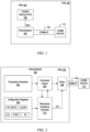
- FIG. 1 is a simplified block diagram of a communication interface (COMM I/F) 102 provided on a printed circuit board (PCB) 100 configured with a power distribution network (PDN) 104.
- a power regulator 106 is provided on the PCB 100 to provide power to various components and devices also provided on or within the PCB 100. As shown, for example, the power regulator 106 generates a supply voltage VDD provided to a supply input of a processor 108.
- the communication interface 102 is coupled between the processor 108 and a communication device 110 also mounted on the PCB 100 to enable communications between the processor 108 and the communication device 110.
- the processor 108 may be configured in any suitable manner depending upon the application and corresponding implementation, such as a multiprocessor, a microprocessor, a micro-processing unit (MPU), a microcontroller, a central processing unit (CPU), etc., or any other type of processing circuitry that may be known or further developed.
- the communication device 110 may be any type of device, such as a bus controller, a peripheral device, a memory system, a bridge interface, etc.
- a memory system may be implemented according to any type of random-access memory (RAM), which may include a double data rate (DDR) memory such as a DDR synchronous dynamic RAM (SDRAM) class of memory or the like.
- DDR double data rate
- SDRAM DDR synchronous dynamic RAM
- the communication device 110 may also receive power from the power regulator 106, it is not shown within the PDN 104 and thus may be powered separately by other power circuitry (not shown).
- the PDN 104 is depicted as a shaded area which generally represents distribution of power on the PCB 100 by the power regulator 106.
- the PDN 104 incorporates the conductive traces on one or more layers of the PCB 100 along with conductive vias and the like for distributing supply voltage and current on the PCB 100.
- the PDN 104 also represents the physical and electrical characteristics of power distribution, such as physical or inherent resistances, capacitances, and inductances that have either or both electrical influence and electromagnetic interference on power distribution and the devices receiving power.
- the processor 108 for example, is also depicted with shading to illustrate that the PDN 104 is distributed throughout and thus effectively permeates the processor 108 and its circuitry.
- the communication interface 102 is depicted with shading to illustrate impact of the PDN 104 on communications that occur on the communication interface 102.
- the PDN 104 has a resonant frequency F PDN .
- communications on the communication interface 102 between the processor 108 and the communication device 110 that operate at or sufficiently near F PDN may stimulate the PDN 104, which may cause substantial degradation in the supply voltage to the on-die circuitry of the processor 108 and thereby on the quality of the signalling on the communication interface 102.
- Such stimulation and interference can cause the communication interface 102 to suffer single bit errors, multibit errors, or to fail altogether.
- a system and method of controlling a communication interface to avoid stimulating power distribution resonance as described herein prevents these errors or failures by intentionally avoiding the combination of activation and inactivation at or sufficiently near the resonant frequency F PDN of the PDN 104.
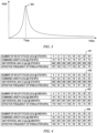
- FIG. 2 is a simplified block diagram of the processor 108 coupled to the communication interface 102 according to one embodiment, in which the communication interface 102 is coupled to the communication device 110.
- the illustrated processor 108 includes a transaction scheduler 202, a command queue 204, a driver 206 (which may further include arbitration circuitry), a set of configuration registers 208, and a resonance avoidance controller 210.
- the illustrated processor 108 is also shown shaded to represent distribution of the PDN 104 throughout the integrated or semiconductor chip structure of the processor 108 including its attachment method to the PCB 100 (e.g., ball-grid array or the like).
- the command queue 204 may include a first-in, first-out (FIFO) buffer or the like (not shown) filled with commands and any other information to be asserted on the communication interface 102.
- the transaction scheduler 202 monitors operation of the processor 108 and fills the command queue 204 with the commands and other information for carrying out the functions of the processor 108 as it relates to the communication device 110.
- the commands may include write operations along with address and data information for storing data or for retrieving stored data.
- the driver 206 retrieves commands and other information from the command queue 204 and asserts the retrieved information onto the communication interface 102.
- a system and method of controlling a communication interface as described herein is not limited to communications with a memory system but may be applied to any type communication interface with many other types of communication devices.
- the configuration registers 208 store parameters associated with operation of the processor 108 including timing parameters.
- the timing parameters may include an operating rate (OP_RATE) of the processor 108 and the communication interface 102 expressed in units based on the particular configuration.
- OP_RATE is expressed terms of mega-transfers per second per bit (MT/s).
- the OP_RATE value may be related to the operating speed or clock frequency dictating transfer operations on the communication interface 102.
- Example values of OP_RATE include 2800 and 3733, although any other suitable value may be used depending upon the particular configuration.
- the timing parameters may include a unit-interval (UI) value which may be the reciprocal of the OP_RATE with corresponding suitable units.
- UI unit-interval
- UI may be expressed in appropriate time units such as, for example, picoseconds (ps).
- ps picoseconds
- UI may have a value of 1/3733e6 ⁇ 286ps.
- UI may have a value of 1/2800e6 ⁇ 357ps.
- the timing parameters may include a command length (CLEN) of the commands expressed in UI units, such as 16 UIs or 32 UIs or the like.
- the timing parameters may include a resonant frequency period value FPER indicative of a period of the resonant frequency F PDN of the PDN 104.
- the timing parameters may include a separation time (ST) value relative to the period of the resonant frequency F PDN that may be used to determine the amount of delay to be inserted to ensure avoidance of resonance conflict.
- the resonance avoidance controller 210 may use one or more of the timing parameters to identify a resonance conflict condition with the resonant frequency F PDN of the PDN 104.
- a resonance conflict condition occurs when a time interval between sequential transactions of a communication interface separated by a period of inactivity presents an effective frequency between the sequential transactions that is equal to or sufficiently close to the resonant frequency F PDN of the PDN 104.
- the time interval between the sequential transactions separated by inactivity is at or near the period of the resonant frequency F PDN of the PDN 104.
- a resonance conflict condition occurs when a time interval between sequential commands asserted on the communication interface 102 separated by one or more inactive cycles, or no operation (no-op) commands, presents an effective frequency between the sequential commands that is equal to or sufficiently close to the resonant frequency F PDN of the PDN 104.
- the resonance avoidance controller 210 monitors the command queue 204 to identify potential resonance conflicts based on the identified resonance conflict condition.
- the effective frequency between the sequential transactions may have an effective period EP.
- FPER represents a period of the resonant frequency F PDN of the PDN 104 and if ST represents a separation time relative to FPER
- a resonance conflict occurs when the difference between EP and FPER is less than ST, or when (FPER - ST) ⁇ EP ⁇ (FPER + ST).
- FPER has a value of 10 representing a period of 10 nanoseconds (ns) of a resonant frequency F PDN of the PDN 104 equal to 100 megahertz (MHz).
- OP_RATE is 3733 MT/s so that UI is about 268ps and that the command length is 16 UIs.
- the resonance avoidance controller 210 When the resonance avoidance controller 210 identifies potential resonance conflicts in the command queue 204, it may take remedial action to avoid the conflict. In the general case, the resonance avoidance controller 210 inserts a delay between sequential activity to increase the inactive period to avoid an effective frequency at or near the resonant frequency of the PDN 104.
- the ST value may be used to determine the amount of delay that may be needed to increase the period of the effective frequency to avoid the resonance conflict.
- the ST may represent a worst-case condition when the time interval between sequential transactions separated by inactivity exactly matches the period of F PDN .
- the ST value may be determined experimentally or empirically for a given configuration to adjust the period of the effective frequency by a sufficient amount to ensure that stimulation of the PDN 104 avoids errors of the communication interface 102.
- the resonance avoidance controller 210 revises the entries in the FIFO of the command queue 204, such as by inserting one or more additional no-ops between the resonance conflicting sequential commands.
- the resonance avoidance controller 210 determines a difference in time between the period of the effective frequency of the potentially conflicting transactions or commands and the period of F PDN as indicated by or otherwise determined from FPER.
- the resonance avoidance controller 210 compares the time difference with ST to determine a minimum time differential representing the minimum amount of adjustment to avoid conflict.
- the resonance avoidance controller 210 selects a number of no-ops that equals or exceeds the minimum time differential and inserts the requisite number of no-ops between the sequential transactions.
- the resonance avoidance controller 210 may insert an additional 8 no-ops for a total of 28 no-ops to achieve a period of 12ns corresponding with an effective frequency of about 85MHz, which is sufficiently separated from the resonant frequency of 100MHz to minimize or otherwise substantially reduce the potential resonance interference.
- the resonance avoidance controller 210 may directly control the driver 206 to insert a delay between sequential commands to avoid resonance conflict.
- the resonance avoidance controller 210 may still monitor the command queue 204 to identify when commands are output to be driven onto the communication interface 102 by the driver 206.
- the resonance avoidance controller 210 may assert a delay (DLY) signal to the driver 206, causing the driver 206 to pause between successive commands to avoid a resonance conflict.
- DLY delay
- the amount of delay to insert may be determined based on ST in a similar manner previously described. In this case, however, the time differential may be inserted directly rather than first converting to a corresponding number of no-ops.
- the driver 206 may pause for an indicated amount of time, such as while the DLY signal is asserted, to implement the delay.
- the resonance avoidance controller 210 may assert the DLY signal after completion of the first command and before completion of the second command for an amount of time determined by the resonance avoidance controller 210 to minimize the potential resonance interference.
- FIG. 3 is a graphic diagram plotting impedance of the PDN 104 (IPDN) versus frequency (FREQ). Frequency is measured in an applicable factor of Hertz, such as MHz or the like.
- a frequency F PDN occurs when IPDN reaches a peak value as shown at 302.
- F PDN may be determined by simulation, experimentally or empirically during testing of the PCB 100. Once known, the FPER value is determined and stored for copying into a corresponding one of the configuration registers 208 during operation.
- the resonance avoidance controller 210 accesses and uses this value as previously described to avoid resonance conflicts with the PDN 104.
- FIG. 4 is a series of tables 401, 402, 403, and 404 illustrating examples of determining the effective frequency of stimulation for different operation conditions of the processor 108 and communication interface 102 according to one embodiment.
- the first two tables 401 and 402 list values for an operating rate of 3733 MT/s with a UI of about 268ps
- the second two tables 403 and 404 list values for an operating rate of 2800 MT/s with a UI of about 357ps, and are reproduced below: TABLE 401 NUMBER OF NO-OP CYCLES (UI's) @ 3733 4 8 12 16 20 24 28 32 COMMAND LENGTH (UI's) @ 3733 MT/s 16 16 16 16 16 16 16 16 16 16 16 UNIT INTERVAL
- the first and third tables 401 and 403 list values for a command length the 16 UI's and the second and fourth tables 402 and 404 list values for a command length of 32 UI's.
- Each of the tables 401 - 404 list an effective frequency value in MHz for each of a different number of no-op cycles measured in UI's.
- the effective frequency of stimulation is 100MHz for 2800 MT/s with 4 no-ops.
- the specific values listed are exemplary only and determined for a particular implementation and may be different for different configurations and implementations.
- FIG. 5 is a timing diagram plotting transaction signals on the communication interface 102 illustrating extreme stimulation of the PDN 104 potentially resulting in resonance conflict according to one embodiment.
- the transactions are memory write transaction signals for the case in which the communication device 110 is in the form of a memory system and the communication interface 102 is a memory interface such as a memory bus or the like.
- Alternative configurations of the communication interface 102 and the communication device 110 are contemplated in which the present disclosure is not limited to memory transactions.
- the plotted signals include a clock signal CLK, a toggling signal representing a write command WCMD, and a toggling signal representing DATA to be written.
- the address may be incorporated within the write command or asserted on separate signals.
- a first write command WCMD1 and corresponding data DATA1 is asserted onto the communication interface 102 beginning at a time t0.
- the data DATA1 of the first write command completes at a subsequent time 11, which is followed by inactivity from time t1 to a time t2.
- the period of inactivity may be filled with any number of no-op cycles.
- a second write command WCMD2 and corresponding data DATA2 is asserted onto the communication interface 102 beginning at time t2.
- the elapsed time between times t0 and t2 is a delta time ⁇ t which is approximately equal to 1/F PDN of the PDN 104.
- the first and second sequential commands WCMD1 and WCMD2 separated by a period of inactivity with start times having a time interval at or near the F PDN of the PDN 104 causes a resonance conflict with the PDN 104.
- This situation represents an extreme stimulation event of the PDN 104 which may cause bit errors or even failure of the transactions being asserted on the communication interface 102.
- FIG. 6 is a timing diagram plotting memory transaction signals that may be asserted on the communication interface 102 illustrating mild stimulation of the PDN 104 that avoids resonance conflict according to one embodiment.
- the same signals as FIG. 5 are plotted, including the clock signal CLK, the write commands WCMD1 and WCMD1 and corresponding data signals DATA1 and DATA2, respectively.
- the second write command WCMD2 and corresponding data DATA2 are not asserted onto the communication interface 102 at time t2 but instead are delayed until a subsequent time t3.
- the resonance avoidance controller 210 either inserts additional no-ops or delays the driver 206 by a time difference between times t2 and t3.
- the elapsed time between times t0 and t3 is a delta time ⁇ t which is substantially different from 1/F PDN of the PDN 104.
- This situation represents a mild stimulation event of the PDN 104 thereby avoiding bit errors or even failure of the transactions being asserted on the communication interface 102.
- Resonance avoidance such as performed by the resonance avoidance controller 210, is configured to adjust operation to intentionally avoid stimulating the system at or near F PDN .
- Programmable control of the duration of inactivity between sequential commands prevents the combination(s) of activity and inactivity which might otherwise combine to create a time period approximately equal to the time period corresponding to F PDN .
- Resonance avoidance enables a communication interface to operate at a higher speed or at the same speed but with a less costly power distribution network.
- the relative impact varies depending on many factors. For example, in a DDR memory system, most data are transmitted via streaming in which commands are executed back-to-back without intermediate periods of inactivity. Such streaming does not pose a problematic scenario since although many bits can switch, not all the possible bits switch, so that resonance avoidance does not need to modify the most common transactions.
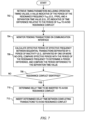
- FIG. 7 is a flowchart diagram illustrating operation of the resonance avoidance controller 210 according to one embodiment.
- the resonance avoidance controller 210 retrieves timing parameters including operation timing values, a value indicative of the period of the resonance frequency F PDN (e.g., FPER), and a separation time value (e.g., ST) relative to the period of F PDN to avoid resonance conflict.
- F PDN the resonance frequency
- ST separation time value
- the timing parameters OP_RATE, CLEN, UI, FPER, and ST may be retrieved from the configuration registers 208.
- Operation advances to block 704, in which the resonance avoidance controller 210 monitors pending transactions of the communication interface 102.
- the resonance avoidance controller 210 may monitor the commands or other transactions in the command queue 204.
- the "effective period" of the effective frequency between each pair of sequential transactions that are separated by a period of inactivity is calculated.
- the effective period is then compared with the period of the resonance frequency to determine a period difference.
- Each period difference reflects the frequency difference between the effective frequency of a corresponding pair of sequential transactions and the resonance frequency F PDN .
- the calculated period difference is then compared to the separation time value, such as ST in the illustrated embodiment of FIG. 2 .
- a resonance conflict is identified when a pair of sequential transactions or commands separated by inactivity also having a time interval at or near the period of F PDN .
- Each calculated period difference that is equal to or greater than the separation time value means that stimulation is sufficiently mild so that correction by added delay is not necessary.
- the corresponding stimulation may be sufficiently disruptive and represents a resonance conflict.
- operation advances instead to block 710 in which a delay time is determined that avoids the resonance conflict when inserted between the identified sequential transactions that would otherwise have a conflicting effective frequency.
- the added delay represents changing the effective period to more than FPER + ST to avoid resonance conflict.
- the added delay may be as much as 2*ST, such as when the initial effective period is about equal to FPER - ST.
- the delay time is inserted between the conflicting transactions to avoid the resonance conflict.
- a number of no-ops is determined having a total delay time that equals or exceeds the minimum amount of delay time to achieve a period of at least PPER + ST, and that number of no-ops is inserted between the conflicting commands, such as, for example, within the command queue 204.
- the minimum time period is added by simply delaying the second transaction, such as, for example, delaying the driver 206 after the first command before allowing the second command to be asserted onto the communication interface 102.
- operation loops back to block 704 to continue monitoring the pending transactions. Operation repeats in this manner during operation.
- circuitry states such as circuitry low and circuitry high may be reversed depending upon whether the pin or signal is implemented in positive or negative circuitry or the like.
- the circuitry state may be programmable in which the circuitry state may be reversed for a given circuitry function.
Landscapes
- Engineering & Computer Science (AREA)
- Power Engineering (AREA)
- General Engineering & Computer Science (AREA)
- Physics & Mathematics (AREA)
- General Physics & Mathematics (AREA)
- Computer Networks & Wireless Communication (AREA)
- Signal Processing (AREA)
- Theoretical Computer Science (AREA)
- Automation & Control Theory (AREA)
- Communication Control (AREA)
Abstract
Description
- The present invention relates in general to a communication systems, and more particularly to a system and method of controlling a communication interface to avoid a conflict with power distribution resonance.
- Certain combinations of communication activity on a communication interface may stimulate the system power distribution network (PDN) at its resonant frequency, causing an impact on the supply voltage provided to on-die circuitry driving the communication interface and potentially causing substantial degradation in the quality of the signalling on the communication interface. The power distribution network resonance stimulation may cause interference on the communication interface, which may cause the interface to suffer single bit errors or multibit errors or may even cause the communication interface to fail altogether.
- Embodiments of the present invention are illustrated by way of example and are not limited by the accompanying figures. Similar references in the figures may indicate similar elements. Elements in the figures are illustrated for simplicity and clarity and have not necessarily been drawn to scale.
-
FIG. 1 is a simplified block diagram of a communication interface provided on a printed circuit board configured with a power distribution network (PDN). -
FIG. 2 is a simplified block diagram of the processor coupled to the communication interface ofFIG. 1 according to one embodiment, in which the communication interface is coupled to the communication device ofFIG. 1 . -
FIG. 3 is a graphic diagram plotting impedance versus frequency of the PDN ofFIG. 1 . -
FIG. 4 is a series of tables illustrating examples of determining the effective frequency of stimulation for different operation conditions of the processor and communication interface ofFIG. 1 according to one embodiment. -
FIG. 5 is a timing diagram plotting transaction signals on the communication interface ofFIG. 1 illustrating extreme stimulation of the PDN potentially resulting in resonance conflict according to one embodiment in which the communication interface is configured as a memory interface. -
FIG. 6 is a timing diagram plotting memory transaction signals that may be asserted on the communication interface illustrating mild stimulation of the PDN ofFIG. 1 that avoids resonance conflict according to one embodiment. -
FIG. 7 is a flowchart diagram illustrating operation of the resonance avoidance controller ofFIG. 2 according to one embodiment. - As described herein, a "resonance conflict" occurs when an effective frequency of an event in circuitry is sufficiently close to the resonant frequency of the power distribution network (PDN) to cause stimulation of the PDN resonance. Such resonance conflict is particularly disadvantageous on a communication interface, since stimulation of the PDN resonance may cause interference on the communication interface that causes the communication interface to suffer single bit errors or multibit errors or may even cause the communication interface to fail altogether. Conventional methods have been used to resolve the PDN resonance stimulation issue. Such conventional methods, however, are costly, complex, or generally undesirable for a variety of reasons.
- One conventional approach is to increase the amount of on-die power supply decoupling capacitance, which increases die area and cost. Another conventional approach is improving parasitic power supply inductance of the semiconductor package, which often results in changing to a higher cost package or appropriating resources from other power supplies. Another conventional approach is adding package decoupling capacitors, which adds significant cost to the customer bill of materials (BOM) or is often not feasible depending on the ball-grid array pitch of the configuration. Another conventional approach is improving the board level parasitic power supply inductance, which means, in practice, either increasing layer count or reorganizing the stack-up with additional cost and complexity. Another conventional approach is slowing down the communication interface altogether to shift away from resonant frequency stimulation of the PDN, which negatively impacts performance.
- A system and method of controlling a communication interface to avoid the PDN resonance conflict as described herein prevents errors or failures otherwise caused by stimulation of PDN resonance by intentionally avoiding the combination of activation and inactivation on the communication interface that has an effective frequency that is at or near the resonant frequency of the power distribution network.
-
FIG. 1 is a simplified block diagram of a communication interface (COMM I/F) 102 provided on a printed circuit board (PCB) 100 configured with a power distribution network (PDN) 104. Apower regulator 106 is provided on the PCB 100 to provide power to various components and devices also provided on or within thePCB 100. As shown, for example, thepower regulator 106 generates a supply voltage VDD provided to a supply input of aprocessor 108. Thecommunication interface 102 is coupled between theprocessor 108 and acommunication device 110 also mounted on the PCB 100 to enable communications between theprocessor 108 and thecommunication device 110. - The
processor 108 may be configured in any suitable manner depending upon the application and corresponding implementation, such as a multiprocessor, a microprocessor, a micro-processing unit (MPU), a microcontroller, a central processing unit (CPU), etc., or any other type of processing circuitry that may be known or further developed. Thecommunication device 110 may be any type of device, such as a bus controller, a peripheral device, a memory system, a bridge interface, etc. As an example, a memory system may be implemented according to any type of random-access memory (RAM), which may include a double data rate (DDR) memory such as a DDR synchronous dynamic RAM (SDRAM) class of memory or the like. Although thecommunication device 110 may also receive power from thepower regulator 106, it is not shown within thePDN 104 and thus may be powered separately by other power circuitry (not shown). - The PDN 104 is depicted as a shaded area which generally represents distribution of power on the
PCB 100 by thepower regulator 106. The PDN 104 incorporates the conductive traces on one or more layers of thePCB 100 along with conductive vias and the like for distributing supply voltage and current on thePCB 100. The PDN 104 also represents the physical and electrical characteristics of power distribution, such as physical or inherent resistances, capacitances, and inductances that have either or both electrical influence and electromagnetic interference on power distribution and the devices receiving power. Theprocessor 108, for example, is also depicted with shading to illustrate that the PDN 104 is distributed throughout and thus effectively permeates theprocessor 108 and its circuitry. In addition, since coupled to theprocessor 108, thecommunication interface 102 is depicted with shading to illustrate impact of thePDN 104 on communications that occur on thecommunication interface 102. - The PDN 104 has a resonant frequency FPDN. As described further herein, communications on the
communication interface 102 between theprocessor 108 and thecommunication device 110 that operate at or sufficiently near FPDN may stimulate thePDN 104, which may cause substantial degradation in the supply voltage to the on-die circuitry of theprocessor 108 and thereby on the quality of the signalling on thecommunication interface 102. Such stimulation and interference can cause thecommunication interface 102 to suffer single bit errors, multibit errors, or to fail altogether. A system and method of controlling a communication interface to avoid stimulating power distribution resonance as described herein prevents these errors or failures by intentionally avoiding the combination of activation and inactivation at or sufficiently near the resonant frequency FPDN of thePDN 104. -
FIG. 2 is a simplified block diagram of theprocessor 108 coupled to thecommunication interface 102 according to one embodiment, in which thecommunication interface 102 is coupled to thecommunication device 110. The illustratedprocessor 108 includes atransaction scheduler 202, acommand queue 204, a driver 206 (which may further include arbitration circuitry), a set ofconfiguration registers 208, and aresonance avoidance controller 210. The illustratedprocessor 108 is also shown shaded to represent distribution of thePDN 104 throughout the integrated or semiconductor chip structure of theprocessor 108 including its attachment method to the PCB 100 (e.g., ball-grid array or the like). In one embodiment, thecommand queue 204 may include a first-in, first-out (FIFO) buffer or the like (not shown) filled with commands and any other information to be asserted on thecommunication interface 102. Thetransaction scheduler 202 monitors operation of theprocessor 108 and fills thecommand queue 204 with the commands and other information for carrying out the functions of theprocessor 108 as it relates to thecommunication device 110. When thecommunication device 110 is configured as a memory system, for example, the commands may include write operations along with address and data information for storing data or for retrieving stored data. Thedriver 206 retrieves commands and other information from thecommand queue 204 and asserts the retrieved information onto thecommunication interface 102. - It is noted that a system and method of controlling a communication interface as described herein is not limited to communications with a memory system but may be applied to any type communication interface with many other types of communication devices.
- The configuration registers 208 store parameters associated with operation of the
processor 108 including timing parameters. The timing parameters may include an operating rate (OP_RATE) of theprocessor 108 and thecommunication interface 102 expressed in units based on the particular configuration. In one embodiment, OP_RATE is expressed terms of mega-transfers per second per bit (MT/s). The OP_RATE value may be related to the operating speed or clock frequency dictating transfer operations on thecommunication interface 102. Example values of OP_RATE include 2800 and 3733, although any other suitable value may be used depending upon the particular configuration. The timing parameters may include a unit-interval (UI) value which may be the reciprocal of the OP_RATE with corresponding suitable units. In one embodiment, for OP_RATE expressed in units of MT/s, UI may be expressed in appropriate time units such as, for example, picoseconds (ps). For an OP_RATE value of 3733 MT/s, UI may have a value of 1/3733e6 ≈ 286ps. For an OP_RATE value of 2800 MT/s, UI may have a value of 1/2800e6 ≈ 357ps. Alternative values are contemplated. The timing parameters may include a command length (CLEN) of the commands expressed in UI units, such as 16 UIs or 32 UIs or the like. The timing parameters may include a resonant frequency period value FPER indicative of a period of the resonant frequency FPDN of thePDN 104. The timing parameters may include a separation time (ST) value relative to the period of the resonant frequency FPDN that may be used to determine the amount of delay to be inserted to ensure avoidance of resonance conflict. - The
resonance avoidance controller 210 may use one or more of the timing parameters to identify a resonance conflict condition with the resonant frequency FPDN of thePDN 104. In the general case, a resonance conflict condition occurs when a time interval between sequential transactions of a communication interface separated by a period of inactivity presents an effective frequency between the sequential transactions that is equal to or sufficiently close to the resonant frequency FPDN of thePDN 104. In other words, the time interval between the sequential transactions separated by inactivity is at or near the period of the resonant frequency FPDN of thePDN 104. In the illustrated configuration, a resonance conflict condition occurs when a time interval between sequential commands asserted on thecommunication interface 102 separated by one or more inactive cycles, or no operation (no-op) commands, presents an effective frequency between the sequential commands that is equal to or sufficiently close to the resonant frequency FPDN of thePDN 104. In the illustrated embodiment, theresonance avoidance controller 210 monitors thecommand queue 204 to identify potential resonance conflicts based on the identified resonance conflict condition. - In general, the effective frequency between the sequential transactions may have an effective period EP. If FPER represents a period of the resonant frequency FPDN of the
PDN 104 and if ST represents a separation time relative to FPER, then a resonance conflict occurs when the difference between EP and FPER is less than ST, or when (FPER - ST) < EP < (FPER + ST). When a resonance conflict is detected, a delay DEL is added between the sequential transactions to move the effective period to an adjusted effective period AEP outside of the resonance conflict range, so that EP + DEL = AEP > (FPER + ST). It is appreciated that if EP is about equal to (FPER - ST) and since delay always increases the effective period between successive transactions, then the DEL may be as high as 2*ST (e.g., FPER - ST + 2*ST = FPER + ST). - Suppose, for example, that FPER has a value of 10 representing a period of 10 nanoseconds (ns) of a resonant frequency FPDN of the
PDN 104 equal to 100 megahertz (MHz). Also, assume that OP_RATE is 3733 MT/s so that UI is about 268ps and that the command length is 16 UIs. In this example, if first and second sequential commands within thecommand queue 204 are separated by 20 no-ops of one UI each, then the time interval between the commands is 16 + 20 = 36 UI's multiplied by 268ps = 9.65 nanoseconds (ns), having an effective frequency of 1/9.65ns ≈ 104 MHz. The effective frequency of the first and second sequential commands separated by 20 UI's is about 104MHz, which is sufficiently close to FPDN of thePDN 104 = 100 MHz to cause a resonance conflict that may interfere with the transactions asserted on thecommunication interface 102. It is noted that rather than comparing frequency, theresonance avoidance controller 210 may compare the difference between the period of the resonant frequency with the period of the effective frequency for more directly determining the delay to be inserted. Thus, it may be determined that a period of 9.65 (ns) of the effective frequency of the sequential commands is sufficiently close to the period of 10 (ns) of the resonant frequency. - When the
resonance avoidance controller 210 identifies potential resonance conflicts in thecommand queue 204, it may take remedial action to avoid the conflict. In the general case, theresonance avoidance controller 210 inserts a delay between sequential activity to increase the inactive period to avoid an effective frequency at or near the resonant frequency of thePDN 104. The ST value may be used to determine the amount of delay that may be needed to increase the period of the effective frequency to avoid the resonance conflict. The ST may represent a worst-case condition when the time interval between sequential transactions separated by inactivity exactly matches the period of FPDN. The ST value may be determined experimentally or empirically for a given configuration to adjust the period of the effective frequency by a sufficient amount to ensure that stimulation of thePDN 104 avoids errors of thecommunication interface 102. - In one embodiment, the
resonance avoidance controller 210 revises the entries in the FIFO of thecommand queue 204, such as by inserting one or more additional no-ops between the resonance conflicting sequential commands. First, theresonance avoidance controller 210 determines a difference in time between the period of the effective frequency of the potentially conflicting transactions or commands and the period of FPDN as indicated by or otherwise determined from FPER. Second, theresonance avoidance controller 210 compares the time difference with ST to determine a minimum time differential representing the minimum amount of adjustment to avoid conflict. Third, theresonance avoidance controller 210 selects a number of no-ops that equals or exceeds the minimum time differential and inserts the requisite number of no-ops between the sequential transactions. In the example above, theresonance avoidance controller 210 may insert an additional 8 no-ops for a total of 28 no-ops to achieve a period of 12ns corresponding with an effective frequency of about 85MHz, which is sufficiently separated from the resonant frequency of 100MHz to minimize or otherwise substantially reduce the potential resonance interference. - In another embodiment, the
resonance avoidance controller 210 may directly control thedriver 206 to insert a delay between sequential commands to avoid resonance conflict. Theresonance avoidance controller 210 may still monitor thecommand queue 204 to identify when commands are output to be driven onto thecommunication interface 102 by thedriver 206. In addition, as shown, theresonance avoidance controller 210 may assert a delay (DLY) signal to thedriver 206, causing thedriver 206 to pause between successive commands to avoid a resonance conflict. The amount of delay to insert may be determined based on ST in a similar manner previously described. In this case, however, the time differential may be inserted directly rather than first converting to a corresponding number of no-ops. Thedriver 206 may pause for an indicated amount of time, such as while the DLY signal is asserted, to implement the delay. In the example described previously, theresonance avoidance controller 210 may assert the DLY signal after completion of the first command and before completion of the second command for an amount of time determined by theresonance avoidance controller 210 to minimize the potential resonance interference. -
FIG. 3 is a graphic diagram plotting impedance of the PDN 104 (IPDN) versus frequency (FREQ). Frequency is measured in an applicable factor of Hertz, such as MHz or the like. A frequency FPDN occurs when IPDN reaches a peak value as shown at 302. FPDN may be determined by simulation, experimentally or empirically during testing of thePCB 100. Once known, the FPER value is determined and stored for copying into a corresponding one of the configuration registers 208 during operation. Theresonance avoidance controller 210 accesses and uses this value as previously described to avoid resonance conflicts with thePDN 104. -
FIG. 4 is a series of tables 401, 402, 403, and 404 illustrating examples of determining the effective frequency of stimulation for different operation conditions of theprocessor 108 andcommunication interface 102 according to one embodiment. The first two tables 401 and 402 list values for an operating rate of 3733 MT/s with a UI of about 268ps, and the second two tables 403 and 404 list values for an operating rate of 2800 MT/s with a UI of about 357ps, and are reproduced below:TABLE 401 NUMBER OF NO-OP CYCLES (UI's) @ 3733 4 8 12 16 20 24 28 32 COMMAND LENGTH (UI's) @ 3733 MT/s 16 16 16 16 16 16 16 16 UNIT INTERVAL AKA UI (ps) @ 3733 MT/s 268 268 268 268 268 268 268 268 EFFECTIVE FREQUENCY OF 187 155 133 117 104 93 85 78 TABLE 402 NUMBER OF NO-OP CYCLES (UI's) @ 3733 4 8 12 16 20 24 28 32 COMMAND LENGTH (UI's) @ 3733 MT/s 16 16 16 16 16 16 16 16 UNIT INTERVAL AKA UI (ps) @ 3733 MT/s 268 268 268 268 268 268 268 268 EFFECTIVE FREQUENCY OF 187 155 133 117 104 93 85 78 TABLE 403 NUMBER OF NO-OP CYCLES (UI's) @ 2800 4 8 12 16 20 24 28 32 COMMAND LENGTH (UI's) @ 2800 MT/s 16 16 16 16 16 16 16 16 UNIT INTERVAL AKA UI (ps) @ 2800 MT/s 357 357 357 357 357 357 357 357 EFFECTIVE FREQUENCY OF 175 140 117 100 87 78 70 64 TABLE 404 NUMBER OF NO-OP CYCLES (UI's) @ 2800 4 8 12 16 20 24 28 32 COMMAND LENGTH (UI's) @ 2800 MT/s 32 32 32 32 32 32 32 32 UNIT INTERVAL AKA UI (ps) @ 2800 MT/s 357 357 357 357 357 357 357 357 EFFECTIVE FREQUENCY OF 100 87 78 70 64 58 54 50 - The first and third tables 401 and 403 list values for a command length the 16 UI's and the second and fourth tables 402 and 404 list values for a command length of 32 UI's. Each of the tables 401 - 404 list an effective frequency value in MHz for each of a different number of no-op cycles measured in UI's. In the last table 404, for example, the effective frequency of stimulation is 100MHz for 2800 MT/s with 4 no-ops. The specific values listed are exemplary only and determined for a particular implementation and may be different for different configurations and implementations.
-
FIG. 5 is a timing diagram plotting transaction signals on thecommunication interface 102 illustrating extreme stimulation of thePDN 104 potentially resulting in resonance conflict according to one embodiment. In this example, the transactions are memory write transaction signals for the case in which thecommunication device 110 is in the form of a memory system and thecommunication interface 102 is a memory interface such as a memory bus or the like. Alternative configurations of thecommunication interface 102 and thecommunication device 110 are contemplated in which the present disclosure is not limited to memory transactions. The plotted signals include a clock signal CLK, a toggling signal representing a write command WCMD, and a toggling signal representing DATA to be written. The address may be incorporated within the write command or asserted on separate signals. A first write command WCMD1 and corresponding data DATA1 is asserted onto thecommunication interface 102 beginning at a time t0. The data DATA1 of the first write command completes at a subsequent time 11, which is followed by inactivity from time t1 to a time t2. The period of inactivity may be filled with any number of no-op cycles. A second write command WCMD2 and corresponding data DATA2 is asserted onto thecommunication interface 102 beginning at time t2. In this case, the elapsed time between times t0 and t2 is a delta time Δt which is approximately equal to 1/FPDN of thePDN 104. In this manner, the first and second sequential commands WCMD1 and WCMD2 separated by a period of inactivity with start times having a time interval at or near the FPDN of thePDN 104 causes a resonance conflict with thePDN 104. This situation represents an extreme stimulation event of thePDN 104 which may cause bit errors or even failure of the transactions being asserted on thecommunication interface 102. -
FIG. 6 is a timing diagram plotting memory transaction signals that may be asserted on thecommunication interface 102 illustrating mild stimulation of thePDN 104 that avoids resonance conflict according to one embodiment. The same signals asFIG. 5 are plotted, including the clock signal CLK, the write commands WCMD1 and WCMD1 and corresponding data signals DATA1 and DATA2, respectively. In this case, however, the second write command WCMD2 and corresponding data DATA2 are not asserted onto thecommunication interface 102 at time t2 but instead are delayed until a subsequent time t3. Theresonance avoidance controller 210 either inserts additional no-ops or delays thedriver 206 by a time difference between times t2 and t3. In this case, the elapsed time between times t0 and t3 is a delta time Δt which is substantially different from 1/FPDN of thePDN 104. This situation represents a mild stimulation event of thePDN 104 thereby avoiding bit errors or even failure of the transactions being asserted on thecommunication interface 102. - Resonance avoidance, such as performed by the
resonance avoidance controller 210, is configured to adjust operation to intentionally avoid stimulating the system at or near FPDN. Programmable control of the duration of inactivity between sequential commands prevents the combination(s) of activity and inactivity which might otherwise combine to create a time period approximately equal to the time period corresponding to FPDN. Resonance avoidance enables a communication interface to operate at a higher speed or at the same speed but with a less costly power distribution network. The relative impact varies depending on many factors. For example, in a DDR memory system, most data are transmitted via streaming in which commands are executed back-to-back without intermediate periods of inactivity. Such streaming does not pose a problematic scenario since although many bits can switch, not all the possible bits switch, so that resonance avoidance does not need to modify the most common transactions. -
FIG. 7 is a flowchart diagram illustrating operation of theresonance avoidance controller 210 according to one embodiment. At afirst block 702, after power-on or reset (POR), theresonance avoidance controller 210 retrieves timing parameters including operation timing values, a value indicative of the period of the resonance frequency FPDN (e.g., FPER), and a separation time value (e.g., ST) relative to the period of FPDN to avoid resonance conflict. For theprocessor 108 shown inFIG. 2 , for example, the timing parameters OP_RATE, CLEN, UI, FPER, and ST may be retrieved from the configuration registers 208. Operation advances to block 704, in which theresonance avoidance controller 210 monitors pending transactions of thecommunication interface 102. As previously described, theresonance avoidance controller 210 may monitor the commands or other transactions in thecommand queue 204. - At
next block 706, the "effective period" of the effective frequency between each pair of sequential transactions that are separated by a period of inactivity (e.g., two commands separated by one or more no-ops) is calculated. The effective period is then compared with the period of the resonance frequency to determine a period difference. Each period difference reflects the frequency difference between the effective frequency of a corresponding pair of sequential transactions and the resonance frequency FPDN. The calculated period difference is then compared to the separation time value, such as ST in the illustrated embodiment ofFIG. 2 . - At
next block 708, it is queried whether any resonance conflicts are identified in the pending transactions. As previously described, a resonance conflict is identified when a pair of sequential transactions or commands separated by inactivity also having a time interval at or near the period of FPDN. Each calculated period difference that is equal to or greater than the separation time value means that stimulation is sufficiently mild so that correction by added delay is not necessary. When no conflicts are identified, then operation loops back to block 704. Theresonance avoidance controller 210 may continuously loop betweenblocks - When any calculated period difference is less than the separation time value, then the corresponding stimulation may be sufficiently disruptive and represents a resonance conflict. When a resonance conflict is identified as determined at
block 708, operation advances instead to block 710 in which a delay time is determined that avoids the resonance conflict when inserted between the identified sequential transactions that would otherwise have a conflicting effective frequency. The added delay represents changing the effective period to more than FPER + ST to avoid resonance conflict. As previously described, since delay is always added to increase the effective period between the sequential transactions, the added delay may be as much as 2*ST, such as when the initial effective period is about equal to FPER - ST. - At
next block 712, the delay time is inserted between the conflicting transactions to avoid the resonance conflict. In one embodiment, if the delay time is effectuated by inserting no-ops between commands, then a number of no-ops is determined having a total delay time that equals or exceeds the minimum amount of delay time to achieve a period of at least PPER + ST, and that number of no-ops is inserted between the conflicting commands, such as, for example, within thecommand queue 204. In another embodiment, the minimum time period is added by simply delaying the second transaction, such as, for example, delaying thedriver 206 after the first command before allowing the second command to be asserted onto thecommunication interface 102. After the delay is inserted, operation loops back to block 704 to continue monitoring the pending transactions. Operation repeats in this manner during operation. - In most communication interface configurations, only a minor latency impact occurs when resonance avoidance is enabled or otherwise applicable. In particular, it is rare in most configurations to transact a small amount of data and then start another transfer a short time later, which may be referred to as "bubble" transactions. These relatively rare bubble transactions are likely to cause the resonance conflict scenario that can pathologically stimulate the power distribution network at its resonant frequency, which can lead to errors in or failure of the communication interface. Nonetheless, since such transactions are rare, the overall latency impact to avoid resonance conflict is expected to be minimal.
- Although the present invention has been described in connection with several embodiments, the invention is not intended to be limited to the specific forms set forth herein. On the contrary, it is intended to cover such alternatives, modifications, and equivalents as can be reasonably included within the scope of the invention as defined by the appended claims. For example, variations of positive circuitry or negative circuitry may be used in various embodiments in which the present invention is not limited to specific circuitry polarities, device types or voltage or error levels or the like. For example, circuitry states, such as circuitry low and circuitry high may be reversed depending upon whether the pin or signal is implemented in positive or negative circuitry or the like. In some cases, the circuitry state may be programmable in which the circuitry state may be reversed for a given circuitry function.
- The terms "a" or "an," as used herein, are defined as one or more than one. Also, the use of introductory phrases such as "at least one" and "one or more" in the claims should not be construed to imply that the introduction of another claim element by the indefinite articles "a" or "an" limits any particular claim containing such introduced claim element to inventions containing only one such element, even when the same claim includes the introductory phrases "one or more" or "at least one" and indefinite articles such as "a" or "an." The same holds true for the use of definite articles. Unless stated otherwise, terms such as "first" and "second" are used to arbitrarily distinguish between the elements such terms describe. Thus, these terms are not necessarily intended to indicate temporal or other prioritization of such elements.
Claims (14)
- A resonance avoidance system, comprising:a power distribution network configured to distribute supply voltage, wherein the power distribution network has a power distribution network resonance; andprocessing circuitry coupled to the power distribution network, comprising:a driver that drives transactions onto a communication interface; anda resonance avoidance controller that is configured to insert a delay between sequential transactions separated by an inactive period to avoid stimulating the power distribution network resonance.
- The resonance avoidance system of claim 1, wherein the resonance avoidance controller is configured to insert the delay by delaying a second transaction from being driven onto the communication interface after a first transaction when a time interval between respective start times of the first and second transactions separated by the inactive period is within a predetermined separation time of a period of the power distribution network resonance.
- The resonance avoidance system of claim 1 or 2, wherein the resonance avoidance controller is configured to insert the delay by inserting one or more inactive cycles between the sequential transactions.
- The resonance avoidance system of any preceding claim, wherein the resonance avoidance controller is configured to insert the delay by delaying the driver between the sequential transactions.
- The resonance avoidance system of any preceding claim, wherein the resonance avoidance controller is configured to detect a resonance conflict between a first command and a second command scheduled within a command queue, and to insert the delay by inserting at least one no operation command in the command queue between the first command and the second command.
- The resonance avoidance system of any preceding claim, wherein the resonance avoidance controller is configured to retrieve operational timing values from a configuration circuit, to use the operational timing values to calculate a time interval between respective start times of first and second transactions, and to detect a resonance conflict based on comparing the time interval with a resonant frequency period value.
- The resonance avoidance system of any preceding claim wherein the resonance avoidance controller is configured to retrieve operational timing values from a configuration circuit, to use the operational timing values to calculate an effective frequency of stimulation based on a time interval between start times of first and second transactions, and to detect a resonance conflict based on comparing the effective frequency of stimulation with a resonant frequency period value.
- The resonance avoidance system of any preceding claim, wherein the resonance avoidance controller is configured to calculate an effective period of an effective frequency of the sequential transactions, to compare the effective period with a period of the power distribution network resonance to determine a period difference, and to detect a resonance conflict based on the period difference.
- A method of avoiding stimulation of a power distribution network resonance, comprising:detecting a resonance conflict between the power distribution network resonance and an effective frequency of sequential transactions on a communication interface separated by an inactive period; andinserting a delay between the sequential transactions to avoid stimulating the power distribution network resonance.
- The method of claim 9, wherein the inserting a delay comprises delaying a second transaction from being driven onto the communication interface after a first transaction when a time interval between respective start times of the first and second transactions separated by the inactive period is within a predetermined separation time of a period of the power distribution network resonance.
- The method of claim 9 or 10, wherein the inserting a delay comprises inserting one or more inactive cycles between the sequential transactions.
- The method of any of claims 9 to 11, wherein the inserting a delay comprises delaying a driver that drives transactions onto the communication interface between the sequential transactions.
- The method of any of claims 9 to 12, wherein the detecting a resonance conflict comprises:retrieving operational timing values from a configuration circuit;using the operational timing values to calculate a time interval between respective start times of first and second transactions; andcomparing the time interval with a resonant frequency period value.
- The method of any of claims 9 to 13, wherein the detecting a resonance conflict comprises:calculating an effective period of an effective frequency of the sequential transactions;comparing the effective period with a period of the power distribution network resonance to determine a period difference; anddetecting the resonance conflict based on the period difference.
Applications Claiming Priority (1)
| Application Number | Priority Date | Filing Date | Title |
|---|---|---|---|
| US17/976,523 US12494638B2 (en) | 2022-10-28 | 2022-10-28 | System and method of controlling communication interface to avoid power distribution resonance conflict |
Publications (1)
| Publication Number | Publication Date |
|---|---|
| EP4361831A1 true EP4361831A1 (en) | 2024-05-01 |
Family
ID=88295926
Family Applications (1)
| Application Number | Title | Priority Date | Filing Date |
|---|---|---|---|
| EP23202114.7A Withdrawn EP4361831A1 (en) | 2022-10-28 | 2023-10-06 | System and method of controlling communication interface to avoid power distribution resonance conflict |
Country Status (3)
| Country | Link |
|---|---|
| US (1) | US12494638B2 (en) |
| EP (1) | EP4361831A1 (en) |
| CN (1) | CN117955124A (en) |
Citations (2)
| Publication number | Priority date | Publication date | Assignee | Title |
|---|---|---|---|---|
| US8451913B2 (en) * | 2008-06-20 | 2013-05-28 | Rambus Inc. | Frequency responsive bus coding |
| US20200310520A1 (en) * | 2019-03-29 | 2020-10-01 | Micron Technology, Inc. | Predictive power management |
Family Cites Families (8)
| Publication number | Priority date | Publication date | Assignee | Title |
|---|---|---|---|---|
| US6781355B2 (en) | 2002-10-18 | 2004-08-24 | Sun Microsystems, Inc. | I/O power supply resonance compensation technique |
| US7043379B2 (en) | 2002-10-22 | 2006-05-09 | Sun Microsystems, Inc. | Method for quantifying I/O chip/package resonance |
| US6842351B2 (en) | 2003-02-20 | 2005-01-11 | Sun Microsystems, Inc. | Method and apparatus for I/O resonance compensation |
| WO2009137522A2 (en) | 2008-05-06 | 2009-11-12 | Rambus Inc. | Method and apparatus for power sequence timing to mitigate supply resonance in power distribution network |
| KR20140107890A (en) * | 2013-02-28 | 2014-09-05 | 에스케이하이닉스 주식회사 | Memory, memory system including the same, and operation method of memory controller |
| US9100047B2 (en) * | 2013-09-20 | 2015-08-04 | Intel Corporation | Method and apparatus for mitigating resonant effects within a power delivery network of a printed circuit board |
| US11054891B2 (en) | 2019-05-09 | 2021-07-06 | Google Llc | Resonance aware performance management |
| US11775199B2 (en) * | 2021-01-20 | 2023-10-03 | Micron Technology, Inc. | Voltage resonance mitigation of memory dies |
-
2022
- 2022-10-28 US US17/976,523 patent/US12494638B2/en active Active
-
2023
- 2023-10-06 EP EP23202114.7A patent/EP4361831A1/en not_active Withdrawn
- 2023-10-11 CN CN202311314893.2A patent/CN117955124A/en active Pending
Patent Citations (2)
| Publication number | Priority date | Publication date | Assignee | Title |
|---|---|---|---|---|
| US8451913B2 (en) * | 2008-06-20 | 2013-05-28 | Rambus Inc. | Frequency responsive bus coding |
| US20200310520A1 (en) * | 2019-03-29 | 2020-10-01 | Micron Technology, Inc. | Predictive power management |
Non-Patent Citations (1)
| Title |
|---|
| ANONYMOUS: "NOP (code)", 20 August 2022 (2022-08-20), pages 1 - 8, XP093135205, Retrieved from the Internet <URL:https://en.wikipedia.org/w/index.php?title=NOP_(code)&oldid=1105577347> [retrieved on 20240227] * |
Also Published As
| Publication number | Publication date |
|---|---|
| CN117955124A (en) | 2024-04-30 |
| US20240146053A1 (en) | 2024-05-02 |
| US12494638B2 (en) | 2025-12-09 |
Similar Documents
| Publication | Publication Date | Title |
|---|---|---|
| US7496777B2 (en) | Power throttling in a memory system | |
| US11048284B2 (en) | Self-referenced droop detector circuitry | |
| US12094553B2 (en) | Timing-drift calibration | |
| US11797075B2 (en) | Reducing power consumption of communication interfaces by clock frequency scaling and adaptive interleaving of polling | |
| US10185618B2 (en) | Method and apparatus for selecting one of a plurality of bus interface configurations to use | |
| KR101913549B1 (en) | Semiconductor device and data processing system | |
| JP5392688B2 (en) | Method for calibrating the start value of write leveling in a memory system | |
| EP3324411A1 (en) | A method and apparatus for dynamic memory termination | |
| US20140160874A1 (en) | Power management in semiconductor memory system | |
| US6456544B1 (en) | Selective forwarding of a strobe based on a predetermined delay following a memory read command | |
| US11144410B2 (en) | System and method to dynamically increase memory channel robustness at high transfer rates | |
| CN1732450A (en) | Apparatus and method for bus signal termination compensation during detected quiet cycle | |
| CN100474436C (en) | Methods and apparatus for delay circuit | |
| WO2012064537A2 (en) | Using a stuttered clock signal to reduce self-induced voltage noise | |
| US20060026375A1 (en) | Memory controller transaction scheduling algorithm using variable and uniform latency | |
| US8806233B2 (en) | Power delivery noise reduction on a memory channel | |
| US12494638B2 (en) | System and method of controlling communication interface to avoid power distribution resonance conflict | |
| US7583548B2 (en) | Semiconductor memory apparatus for allocating different read/write operating time to every bank | |
| US7843762B2 (en) | RAM control device and memory device using the same | |
| JP2000163308A (en) | Memory device | |
| US9128716B2 (en) | Memory device and control method |
Legal Events
| Date | Code | Title | Description |
|---|---|---|---|
| PUAI | Public reference made under article 153(3) epc to a published international application that has entered the european phase |
Free format text: ORIGINAL CODE: 0009012 |
|
| STAA | Information on the status of an ep patent application or granted ep patent |
Free format text: STATUS: THE APPLICATION HAS BEEN PUBLISHED |
|
| AK | Designated contracting states |
Kind code of ref document: A1 Designated state(s): AL AT BE BG CH CY CZ DE DK EE ES FI FR GB GR HR HU IE IS IT LI LT LU LV MC ME MK MT NL NO PL PT RO RS SE SI SK SM TR |
|
| STAA | Information on the status of an ep patent application or granted ep patent |
Free format text: STATUS: REQUEST FOR EXAMINATION WAS MADE |
|
| 17P | Request for examination filed |
Effective date: 20241104 |
|
| RBV | Designated contracting states (corrected) |
Designated state(s): AL AT BE BG CH CY CZ DE DK EE ES FI FR GB GR HR HU IE IS IT LI LT LU LV MC ME MK MT NL NO PL PT RO RS SE SI SK SM TR |
|
| STAA | Information on the status of an ep patent application or granted ep patent |
Free format text: STATUS: EXAMINATION IS IN PROGRESS |
|
| 17Q | First examination report despatched |
Effective date: 20241223 |
|
| STAA | Information on the status of an ep patent application or granted ep patent |
Free format text: STATUS: THE APPLICATION HAS BEEN WITHDRAWN |
|
| 18W | Application withdrawn |
Effective date: 20250327 |