EP4358358A1 - Charging module, charging device, and charging system - Google Patents
Charging module, charging device, and charging system Download PDFInfo
- Publication number
- EP4358358A1 EP4358358A1 EP23204099.8A EP23204099A EP4358358A1 EP 4358358 A1 EP4358358 A1 EP 4358358A1 EP 23204099 A EP23204099 A EP 23204099A EP 4358358 A1 EP4358358 A1 EP 4358358A1
- Authority
- EP
- European Patent Office
- Prior art keywords
- switch
- charging
- bus capacitor
- input
- module
- Prior art date
- Legal status (The legal status is an assumption and is not a legal conclusion. Google has not performed a legal analysis and makes no representation as to the accuracy of the status listed.)
- Granted
Links
Images




Classifications
-
- H—ELECTRICITY
- H02—GENERATION; CONVERSION OR DISTRIBUTION OF ELECTRIC POWER
- H02M—APPARATUS FOR CONVERSION BETWEEN AC AND AC, BETWEEN AC AND DC, OR BETWEEN DC AND DC, AND FOR USE WITH MAINS OR SIMILAR POWER SUPPLY SYSTEMS; CONVERSION OF DC OR AC INPUT POWER INTO SURGE OUTPUT POWER; CONTROL OR REGULATION THEREOF
- H02M1/00—Details of apparatus for conversion
- H02M1/42—Circuits or arrangements for compensating for or adjusting power factor in converters or inverters
- H02M1/4208—Arrangements for improving power factor of AC input
- H02M1/4216—Arrangements for improving power factor of AC input operating from a three-phase input voltage
-
- B—PERFORMING OPERATIONS; TRANSPORTING
- B60—VEHICLES IN GENERAL
- B60L—PROPULSION OF ELECTRICALLY-PROPELLED VEHICLES; SUPPLYING ELECTRIC POWER FOR AUXILIARY EQUIPMENT OF ELECTRICALLY-PROPELLED VEHICLES; ELECTRODYNAMIC BRAKE SYSTEMS FOR VEHICLES IN GENERAL; MAGNETIC SUSPENSION OR LEVITATION FOR VEHICLES; MONITORING OPERATING VARIABLES OF ELECTRICALLY-PROPELLED VEHICLES; ELECTRIC SAFETY DEVICES FOR ELECTRICALLY-PROPELLED VEHICLES
- B60L53/00—Methods of charging batteries, specially adapted for electric vehicles; Charging stations or on-board charging equipment therefor; Exchange of energy storage elements in electric vehicles
- B60L53/20—Methods of charging batteries, specially adapted for electric vehicles; Charging stations or on-board charging equipment therefor; Exchange of energy storage elements in electric vehicles characterised by converters located in the vehicle
- B60L53/22—Constructional details or arrangements of charging converters specially adapted for charging electric vehicles
-
- H—ELECTRICITY
- H02—GENERATION; CONVERSION OR DISTRIBUTION OF ELECTRIC POWER
- H02M—APPARATUS FOR CONVERSION BETWEEN AC AND AC, BETWEEN AC AND DC, OR BETWEEN DC AND DC, AND FOR USE WITH MAINS OR SIMILAR POWER SUPPLY SYSTEMS; CONVERSION OF DC OR AC INPUT POWER INTO SURGE OUTPUT POWER; CONTROL OR REGULATION THEREOF
- H02M1/00—Details of apparatus for conversion
- H02M1/14—Arrangements for reducing ripples from DC input or output
-
- H—ELECTRICITY
- H02—GENERATION; CONVERSION OR DISTRIBUTION OF ELECTRIC POWER
- H02M—APPARATUS FOR CONVERSION BETWEEN AC AND AC, BETWEEN AC AND DC, OR BETWEEN DC AND DC, AND FOR USE WITH MAINS OR SIMILAR POWER SUPPLY SYSTEMS; CONVERSION OF DC OR AC INPUT POWER INTO SURGE OUTPUT POWER; CONTROL OR REGULATION THEREOF
- H02M1/00—Details of apparatus for conversion
- H02M1/42—Circuits or arrangements for compensating for or adjusting power factor in converters or inverters
- H02M1/4208—Arrangements for improving power factor of AC input
- H02M1/4233—Arrangements for improving power factor of AC input using a bridge converter comprising active switches
-
- H—ELECTRICITY
- H02—GENERATION; CONVERSION OR DISTRIBUTION OF ELECTRIC POWER
- H02M—APPARATUS FOR CONVERSION BETWEEN AC AND AC, BETWEEN AC AND DC, OR BETWEEN DC AND DC, AND FOR USE WITH MAINS OR SIMILAR POWER SUPPLY SYSTEMS; CONVERSION OF DC OR AC INPUT POWER INTO SURGE OUTPUT POWER; CONTROL OR REGULATION THEREOF
- H02M7/00—Conversion of AC power input into DC power output; Conversion of DC power input into AC power output
- H02M7/42—Conversion of DC power input into AC power output without possibility of reversal
- H02M7/44—Conversion of DC power input into AC power output without possibility of reversal by static converters
- H02M7/48—Conversion of DC power input into AC power output without possibility of reversal by static converters using discharge tubes with control electrode or semiconductor devices with control electrode
- H02M7/483—Converters with outputs that each can have more than two voltages levels
- H02M7/487—Neutral point clamped inverters
-
- H—ELECTRICITY
- H02—GENERATION; CONVERSION OR DISTRIBUTION OF ELECTRIC POWER
- H02J—ELECTRIC POWER NETWORKS; CIRCUIT ARRANGEMENTS OR SYSTEMS FOR SUPPLYING OR DISTRIBUTING ELECTRIC POWER; SYSTEMS FOR STORING ELECTRIC ENERGY
- H02J2207/00—Details of circuit arrangements for charging or discharging batteries or supplying loads from batteries
- H02J2207/20—Charging or discharging characterised by the power electronics converter
-
- H—ELECTRICITY
- H02—GENERATION; CONVERSION OR DISTRIBUTION OF ELECTRIC POWER
- H02J—ELECTRIC POWER NETWORKS; CIRCUIT ARRANGEMENTS OR SYSTEMS FOR SUPPLYING OR DISTRIBUTING ELECTRIC POWER; SYSTEMS FOR STORING ELECTRIC ENERGY
- H02J7/00—Circuit arrangements for charging or discharging batteries or for supplying loads from batteries
- H02J7/02—Circuit arrangements for charging or discharging batteries or for supplying loads from batteries for charging batteries from AC mains by converters
-
- H—ELECTRICITY
- H02—GENERATION; CONVERSION OR DISTRIBUTION OF ELECTRIC POWER
- H02M—APPARATUS FOR CONVERSION BETWEEN AC AND AC, BETWEEN AC AND DC, OR BETWEEN DC AND DC, AND FOR USE WITH MAINS OR SIMILAR POWER SUPPLY SYSTEMS; CONVERSION OF DC OR AC INPUT POWER INTO SURGE OUTPUT POWER; CONTROL OR REGULATION THEREOF
- H02M1/00—Details of apparatus for conversion
- H02M1/0003—Details of control, feedback or regulation circuits
- H02M1/0032—Control circuits allowing low power mode operation, e.g. in standby mode
-
- Y—GENERAL TAGGING OF NEW TECHNOLOGICAL DEVELOPMENTS; GENERAL TAGGING OF CROSS-SECTIONAL TECHNOLOGIES SPANNING OVER SEVERAL SECTIONS OF THE IPC; TECHNICAL SUBJECTS COVERED BY FORMER USPC CROSS-REFERENCE ART COLLECTIONS [XRACs] AND DIGESTS
- Y02—TECHNOLOGIES OR APPLICATIONS FOR MITIGATION OR ADAPTATION AGAINST CLIMATE CHANGE
- Y02B—CLIMATE CHANGE MITIGATION TECHNOLOGIES RELATED TO BUILDINGS, e.g. HOUSING, HOUSE APPLIANCES OR RELATED END-USER APPLICATIONS
- Y02B70/00—Technologies for an efficient end-user side electric power management and consumption
- Y02B70/10—Technologies improving the efficiency by using switched-mode power supplies [SMPS], i.e. efficient power electronics conversion e.g. power factor correction or reduction of losses in power supplies or efficient standby modes
-
- Y—GENERAL TAGGING OF NEW TECHNOLOGICAL DEVELOPMENTS; GENERAL TAGGING OF CROSS-SECTIONAL TECHNOLOGIES SPANNING OVER SEVERAL SECTIONS OF THE IPC; TECHNICAL SUBJECTS COVERED BY FORMER USPC CROSS-REFERENCE ART COLLECTIONS [XRACs] AND DIGESTS
- Y02—TECHNOLOGIES OR APPLICATIONS FOR MITIGATION OR ADAPTATION AGAINST CLIMATE CHANGE
- Y02T—CLIMATE CHANGE MITIGATION TECHNOLOGIES RELATED TO TRANSPORTATION
- Y02T10/00—Road transport of goods or passengers
- Y02T10/60—Other road transportation technologies with climate change mitigation effect
- Y02T10/70—Energy storage systems for electromobility, e.g. batteries
-
- Y—GENERAL TAGGING OF NEW TECHNOLOGICAL DEVELOPMENTS; GENERAL TAGGING OF CROSS-SECTIONAL TECHNOLOGIES SPANNING OVER SEVERAL SECTIONS OF THE IPC; TECHNICAL SUBJECTS COVERED BY FORMER USPC CROSS-REFERENCE ART COLLECTIONS [XRACs] AND DIGESTS
- Y02—TECHNOLOGIES OR APPLICATIONS FOR MITIGATION OR ADAPTATION AGAINST CLIMATE CHANGE
- Y02T—CLIMATE CHANGE MITIGATION TECHNOLOGIES RELATED TO TRANSPORTATION
- Y02T10/00—Road transport of goods or passengers
- Y02T10/60—Other road transportation technologies with climate change mitigation effect
- Y02T10/7072—Electromobility specific charging systems or methods for batteries, ultracapacitors, supercapacitors or double-layer capacitors
Definitions
- This application relates to the field of electrical and electronic technologies, and in particular, to a charging module, a charging device, and a charging system.
- Three-phase Vienna rectifier topology is widely used in a charging system scenario with unidirectional transmission of an active power.
- an active load device and a reactive load device are included in a charging system.
- an extra reactive apparatus usually needs to be disposed for compensation. Therefore, a reactive power regulation function is designed in the Vienna topology to reduce system costs.
- a conventional power factor correction solution In a conventional power factor correction solution: 1. A diode in the Vienna topology is replaced with any one of a metal-oxide-semiconductor field-effect transistor (Metal-Oxide-Semiconductor Field-Effect Transistor, MOSFET)/IGBT, a silicon carbide transistor, a gallium nitride transistor, and another power switch transistor. In this way, bidirectional power flow can be implemented, and a power factor correction function can be implemented. However, in this solution, costs are high. 2. Based on the Vienna topology, a compensation range is determined based on an angle of an input voltage, and a common-mode signal is generated and input into a modulating wave, to change a phase difference between a modulating voltage and the input voltage. However, it is complex to implement this solution, and a current waveform is distorted.
- MOSFET Metal-Oxide-Semiconductor Field-Effect Transistor
- this application provides a charging module, a charging device, and a charging system, so that variable power factor performance of unidirectional power flow topology can be as good as that of bidirectional power flow topology.
- a current waveform and a bus ripple in a working condition with a non-unity power factor can be optimized, and costs can be reduced.
- a first aspect of this application provides a charging module, configured to supply power to a load.
- the charging module includes a three-phase rectifier module, a bus capacitor module, an inductor, and a controller. An input end of the three-phase rectifier module is electrically connected to an input power supply, where an output end of the three-phase rectifier module is electrically connected to an input end of the bus capacitor module, and the three-phase rectifier module includes a three-phase bridge arm.
- the bus capacitor module includes a first bus capacitor and a second bus capacitor, where the first bus capacitor is electrically connected between a first output end of the three-phase bridge arm and a midpoint of the three-phase bridge arm, and the second bus capacitor is electrically connected between a second output end of the three-phase bridge arm and the midpoint.
- the inductor is electrically connected to the midpoint of the three-phase bridge arm and a midpoint between the first bus capacitor and the second bus capacitor.
- the controller is configured to obtain an input voltage and an input current of the charging module, and is further configured to control a status of the three-phase rectifier module based on the input voltage and the input current.
- an inductor is added between a bus midpoint and a three-phase rectifier module in Vienna topology. Because there is no sudden change in a current through an inductor, and the inductor may absorb a part of reactive power and isolate the rectifier module from a bus capacitor, not only a power factor correction function can be implemented, but also there is an effect of improving a bus ripple and a current waveform in a working condition with a non-unity power factor.
- the three-phase rectifier module includes a first switch, a second switch, and a third switch.
- the first switch is electrically connected to a midpoint of a first-phase bridge arm and a first end of the inductor
- a second end of the inductor is electrically connected to the midpoint between the first bus capacitor and the second bus capacitor
- the second switch is electrically connected to a midpoint of a second-phase bridge arm and the first end of the inductor
- the third switch is electrically connected to a midpoint of a third-phase bridge arm and the first end of the inductor.
- the controller is configured to: when it is detected that the input current is less than a current threshold, regulate a phase difference between the input current and the input voltage by controlling the first switch, the second switch, and the third switch.
- the controller is further configured to: when the input power supply charges a reactive load device, regulate the phase difference betweenthe input current and the input voltage by controlling the first switch, the second switch, and the third switch.
- the charging module further includes a fourth switch, the fourth switch is connected in parallel to the inductor, and the fourth switch is further connected to the controller.
- the controller is further configured to control the fourth switch to be on when the charging module needs to work with a unity power factor.
- the controller is further configured to control the fourth switch to be off when the charging module needs to work with a non-unity power factor.
- a second aspect of this application further provides a charging device, configured to supply power to a load and including an input power supply and a charging module.
- the input power supply is configured to supply power to the charging module
- the charging module includes a three-phase rectifier module, a bus capacitor module, an inductor, and a controller.
- An input end of the three-phase rectifier module is electrically connected to an input power supply, where an output end of the three-phase rectifier module is electrically connected to an input end of the bus capacitor module, and the three-phase rectifier module includes a three-phase bridge arm.
- the bus capacitor module includes a first bus capacitor and a second bus capacitor, where the first bus capacitor is electrically connected between a first output end of the three-phase bridge arm and a midpoint of the three-phase bridge arm, and the second bus capacitor is electrically connected between a second output end of the three-phase bridge arm and the midpoint.
- the inductor is electrically connected to the midpoint of the three-phase bridge arm and a midpoint between the first bus capacitor and the second bus capacitor.
- the controller is configured to obtain an input voltage and an input current of the charging module, and is further configured to control a status of the three-phase rectifier module based on the input voltage and the input current.
- an inductor is added between a bus midpoint and a three-phase rectifier module in Vienna topology.
- a power factor correction function can be implemented, and there is an effect of improving a bus ripple and an input current waveform in a working condition with a non-unity power factor.
- the three-phase rectifier module includes a first switch, a second switch, and a third switch.
- the first switch is electrically connected to a midpoint of a first-phase bridge arm and a first end of the inductor
- a second end of the inductor is electrically connected to the midpoint between the first bus capacitor and the second bus capacitor
- the second switch is electrically connected to a midpoint of a second-phase bridge arm and the first end of the inductor
- the third switch is electrically connected to a midpoint of a third-phase bridge arm and the first end of the inductor.
- the charging module further includes a fourth switch, the fourth switch is connected in parallel to the inductor, and the fourth switch is further connected to the controller and a hardware circuit, for example, a peripheral or driver related to the controller.
- the controller is further configured to: control the fourth switch to be on when the charging module needs to work with a unity power factor; and control the fourth switch to be off when the charging module needs to work with a non-unity power factor.
- an embodiment of this application further provides a charging system, including a charging device and one or more electric devices.
- the charging device is electrically connected to the one or more electric devices to charge the one or more electric devices.
- the charging device may include an input power supply and a charging module.
- the input power supply is configured to supply power to the charging module, and the charging module includes a three-phase rectifier module, a bus capacitor module, an inductor, and a controller.
- An input end of the three-phase rectifier module is electrically connected to an input power supply, where an output end of the three-phase rectifier module is electrically connected to an input end of the bus capacitor module, and the three-phase rectifier module includes a three-phase bridge arm.
- the bus capacitor module includes a first bus capacitor and a second bus capacitor, where the first bus capacitor is electrically connected between a first output end of the three-phase bridge arm and a midpoint of the three-phase bridge arm, and the second bus capacitor is electrically connected between a second output end of the three-phase bridge arm and the midpoint.
- the inductor is electrically connected to the midpoint of the three-phase bridge arm and a midpoint between the first bus capacitor and the second bus capacitor.
- the controller is configured to obtain an input voltage and an input current of the input power supply, and is further configured to control a status of the three-phase rectifier module based on the input voltage and the input current.
- an inductor may be added between a bus midpoint and a three-phase rectifier module in Vienna topology. Because there is no sudden change in a current through an inductor, and the inductor may absorb a part of reactive power and isolate the rectifier module from a bus capacitor, not only a power factor correction function can be implemented, but also there is an effect of improving a bus ripple and a current waveform in a working condition with a non-unity power factor.
- the inductor is disposed between the three-phase rectifier module and the midpoint of the bus capacitor module, so that the power factor correction function can be implemented, and there is an effect of improving a bus ripple and an input current waveform in a working condition with a non-unity power factor.
- variable power factor performance of unidirectional power flow topology can be as good as that of bidirectional power flow topology, thereby reducing hardware costs.
- an element when an element is considered to be “connected to” another element, the element may be directly connected to the another element, or there may be an element disposed in between.
- an element When an element is considered to be “disposed” on another element, it may be directly disposed on the another element, or there may be an element disposed in between.
- FIG. 1 is a schematic diagram of an environment in which a charging module is used in an optical storage charging system according to an embodiment of this application.
- the optical storage charging system may include a photovoltaic power generation system 310, an energy storage system 320, a charging station 330, a charging device 340, and a central control unit 350.
- the photovoltaic power generation system 310 may be connected to the energy storage system 320, the charging station 330, and the charging device 340 through a direct current bus.
- the photovoltaic power generation system 310, the energy storage system 320, the charging station 330, and the charging device 340 exchange information with the central control unit 350 through a communication cable or via a communication device.
- the central control unit 350 may be configured to monitor related information, for example, powers of an entire system and each component, and further configured to schedule each power unit.
- the photovoltaic power generation system 310 may include a plurality of photovoltaic panel assemblies 312 and a plurality of DC/DC converters 314.
- the plurality of photovoltaic panel assemblies 312 may be connected to the plurality of DC/DC converters 314 in a one-to-one correspondence.
- the photovoltaic panel assemblies 312 may be power generation apparatuses that are exposed to sunlight and that generate a direct current.
- the photovoltaic panel assemblies 312 may transmit a generated direct voltage to the DC/DC converters 314, and the DC/DC converters 314 may convert the direct voltage from the photovoltaic panel assemblies 312. In this way, the DC/DC converters 314 may transmit the direct voltage on which direct current conversion is performed to the direct current bus of the system through a direct current bus.
- the charging device 340 may include an input power supply 342 and a charging module 100.
- the input power supply 342 may be an alternating current power supply.
- the input power supply 342 may output an alternating voltage to the charging module 100.
- the charging module 100 may be configured to convert the alternating voltage output by the input power supply 342 into a direct voltage.
- the charging module 100 may further transmit the direct voltage obtained through the conversion to the direct current bus, and a load may get energy from the direct current bus.
- the energy storage system 320 may include a DC/DC converter 322 and a plurality of battery packs 324.
- the plurality of battery packs 324 are connected to the DC/DC converter 322.
- the DC/DC converter 322 may receive, through a direct current bus, energy output by the photovoltaic power generation system 310, to charge the plurality of battery packs 324.
- the DC/DC converter 322 may receive, through a direct current bus, energy output by the charging device 340, to charge the plurality of battery packs 324.
- the plurality of battery packs 324 may output a direct voltage to the DC/DC converter 322, and the DC/DC converter 322 may convert the direct voltage output by the plurality of battery packs 324, and output energy to charge the load through a direct current bus.
- the charging station 330 may include a DC/DC converter 332.
- the DC/DC converter 332 may obtain energy and a power from the direct current bus, to supply power to a plurality of electric vehicles 334.
- the charging device 340 and the photovoltaic power generation system 310 may output energy to the direct current bus. Therefore, a load device (for example, the charging station 330) may obtain energy through the direct current bus.
- the energy storage system 320 may output energy to the direct current bus, or the energy storage system 320 may obtain energy through the direct current bus.
- the energy storage system 320 may output energy to the direct current bus, and the load device may obtain, through the direct current bus, the energy output by the energy storage system 320, to supply power to the load device.
- the energy storage system 320 may obtain energy through the direct current bus for storing energy. Therefore, the energy storage system 320 is mainly used for storing energy during off-peak electricity hours and supplying energy during peak electricity hours, so that the entire charging station system maximizes the use of new photovoltaic energy, and consumption of a power grid is reduced.
- FIG. 2 is a schematic diagram of another application environment of a charging module 100 according to an embodiment of this application.
- the charging module 100 may be configured to charge an electric vehicle 200 by using an external power supply. It should be noted that, in another embodiment of this application, the charging module 100 is not limited to being used in the electric vehicle 200.
- the charging module 100 may be a vehicle-mounted charger in the electric vehicle 200.
- An alternating current power grid 210 may output alternating current electrical energy to an alternating current charging pile 220.
- the alternating current charging pile 220 may output alternating current electrical energy to the charging module 100.
- the charging module 100 may process or convert the received alternating current electrical energy, and charge a battery 230 in the electric vehicle 200.
- FIG. 3 is a schematic diagram of another application environment of a charging module 100 according to an embodiment of this application.
- the charging module 100 may be used in a direct current charging pile 250.
- An alternating current power grid 210 may output alternating current electrical energy to a transformer 240.
- the transformer 240 performs conversion and outputs alternating current electrical energy to the direct current charging pile 250.
- the direct current charging pile 250 processes or converts the alternating current electrical energy, and charges a battery 230 in an electric vehicle 200.
- the charging module 100 may be used in a direct current charging pile, a vehicle-mounted charger, a high-power charging pile, an ultra-high-power charging pile, a portable charging pile, or the like.
- FIG. 4 is a schematic diagram of a structure of a charging module 100 according to an embodiment of this application.
- the charging module 100 may be electrically connected to an input power supply 400.
- the input power supply 400 may be a three-phase alternating current power supply, and may supply power to the charging module 100.
- the charging module 100 may include a three-phase rectifier module 10, a bus capacitor module 20, a controller 40, and an inductor L o .
- the bus capacitor module 20 may be electrically connected between the three-phase rectifier module 10 and a load device 30.
- the controller 40 may be connected to the three-phase rectifier module 10, and the controller 40 may control the charging module 100 to perform AC-DC processing by using the three-phase rectifier module 10 in Vienna topology, and correspondingly control a status of a switch in the three-phase rectifier module 10.
- the three-phase rectifier module 10 may be configured to process an output voltage of the input power supply 400.
- the three-phase rectifier module 10 may be configured to convert an alternating voltage output by the input power supply 400 into a direct voltage, and the direct voltage may be used for supplying power to the load device 30.
- the three-phase rectifier module 10 may include a three-phase bridge arm connected in parallel, and the three-phase bridge arm may include a first-phase bridge arm U, a second-phase bridge arm V, and a third-phase bridge arm W.
- the first-phase bridge arm U may include a first diode D1 and a second diode D2.
- the second-phase bridge arm V may include a third diode D3 and a fourth diode D4.
- the third-phase bridge arm W may include a fifth diode D5 and a sixth diode D6.
- an anode of the first diode D1 may be electrically connected to a cathode of the second diode D2
- a cathode of the first diode D1 may be electrically connected to a cathode of the third diode D3 and a cathode of the fifth diode D5
- an anode of the second diode D2 may be electrically connected to an anode of the fourth diode D4 and an anode of the sixth diode D6.
- An anode of the third diode D3 may be electrically connected to a cathode of the fourth diode D4.
- An anode of the fifth diode D5 may be electrically connected to a cathode of the sixth diode D6.
- the cathode of the fifth diode D5 may be further electrically connected to the bus capacitor module 20, and the anode of the sixth diode D6 may be further electrically connected to the bus capacitor module 20.
- the three-phase rectifier module 10 in this embodiment may further include a switch S1, a switch S2, and a switch S3.
- a first end of the switch S1 may be connected to the controller 40, a second end of the switch S1 may be electrically connected to a midpoint A between the first diode D 1 and the second diode D2, and a third end of the switch S1 may be electrically connected to a third end of the switch S2, a third end of the switch S3, and a first end of the inductor L o .
- the first end of the switch S 1 may be used as a control end of the switch S 1, that is, the controller 40 may control a status of the switch S 1.
- the controller 40 may control the switch S1 to be on or off.
- the controller 40 may be in a signal connection to the first end of the switch S1, or the controller 40 may be electrically connected to the first end of the switch S1.
- a first end of the switch S2 may be connected to the controller 40, a second end of the switch S2 may be electrically connected to a midpoint B between the third diode D3 and the fourth diode D4, and a third end of the switch S2 may be electrically connected to the first end of the inductor L o , the third end of the switch S 1, and the third end of the switch S3.
- the first end of the switch S2 may be used as a control end of the switch S2. That is, the controller 40 may control a status of the switch S2.
- the controller 40 may control the switch S2 to be on or off.
- the controller 40 may be in a signal connection to the first end of the switch S2, or the controller 40 may be electrically connected to the first end of the switch S2.
- a first end of the switch S3 may be connected to the controller 40, a second end of the switch S3 may be electrically connected to a midpoint C between the fifth diode D5 and the sixth diode D6, and the third end of the switch S3 may be electrically connected to the first end of the inductor L o , the third end of the switch S 1, and the third end of the switch S2.
- the first end of the switch S3 may be used as a control end of the switch S3. That is, the controller 40 may control a status of the switch S3.
- the controller 40 may control the switch S3 to be on or off.
- the controller 40 may be in a signal connection to the first end of the switch S3, or the controller 40 may be electrically connected to the first end of the switch S3.
- the switches S1 to S3 may each be any one of a metal-oxide-semiconductor field-effect transistor (Metal-Oxide-Semiconductor Field-Effect Transistor, MOSFET) or an insulated gate bipolar transistor (Insulated Gate Bipolar Transistor, IGBT), a silicon carbide transistor, a gallium nitride transistor, and another power switch transistor.
- MOSFET Metal-Oxide-Semiconductor Field-Effect Transistor
- IGBT Insulated Gate Bipolar Transistor
- the three-phase rectifier module 10 may further include a first inductor L a , a second inductor L b , and a third inductor L c .
- a first end of the first inductor L a may be electrically connected to a first output end of the input power supply 400, and a second end of the first inductor L a may be electrically connected to the midpoint A.
- a first end of the second inductor L b may be electrically connected to a second output end of the input power supply 400, and a second end of the second inductor L b may be electrically connected to the midpoint B.
- a first end of the third inductor L c may be electrically connected to a third output end of the input power supply 400, and a second end of the third inductor L c may be electrically connected to the midpoint C.
- the bus capacitor module 20 may include a first bus capacitor C1 and a second bus capacitor C2.
- a first end of the first bus capacitor C1 may be electrically connected to the cathode of the first diode D 1, the cathode of the third diode D3, and the cathode of the fifth diode D5, a second end of the first bus capacitor C1 may be electrically connected to a first end of the second bus capacitor C2, and a second end of the second bus capacitor C2 may be electrically connected to the anode of the second diode D2, the anode of the fourth diode D4, and the anode of the sixth diode D6.
- a second end of the inductor L o may be electrically connected to a midpoint O between the first bus capacitor C1 and the second bus capacitor C2.
- the first inductor L a , the second inductor L b , and the third inductor L c may be configured for energy storage and filtering during on and off of the switch S 1, the switch S2, and the switch S3.
- the bus capacitor module 20 may be configured for energy storage and voltage stabilization of a direct current-side bus.
- the inductor L o is added between the bus capacitor midpoint and the switches S1 to S3. Based on such a design, the charging module in this application can implement a power factor correction function, and can further optimize a current waveform and a bus ripple in a working condition with a non-unity power factor. In this way, variable power factor performance of unidirectional power flow topology can be as good as that of bidirectional power flow topology, thereby reducing hardware costs.
- controller 40 in this embodiment may obtain an input voltage and an input current of the charging module.
- the controller 40 may be configured to control the statuses of the switches S1 to S3 in the charging module 100.
- the charging module 100 may be used for regulating a reactive power of the power grid for reactive power compensation, to achieve reactive power voltage regulation.
- the controller 40 may control the input current to lag the input voltage by using a phase-locked loop, to compensate for a phase difference between the input voltage and the input current caused by a capacitive reactive power, thereby increasing the value of the power factor of the charging module 100.
- Vienna topology is unidirectional power flow topology
- when there is a phase difference between an input voltage and an input current a zero-crossing distortion of a current occurs.
- the inductor L o may be added between a bus midpoint and a switch in the Vienna topology. Because there is no sudden change in a current through the inductor L o , when the current passes through zero, more current flows to an inter-phase switch, and less to the inductor L o at the midpoint and a diode. In this way, a waveform when the current passes through zero is optimized.
- the inductor L o may isolate a voltage at the bus midpoint from a voltage of the inductor, and the inductor may further absorb a part of reactive power. In this way, a bus voltage ripple can be further attenuated, and a bus ripple can be reduced.
- a B-phase current is a reverse current
- a C-phase current is a forward current
- the controller 40 may control the switch S1 and the switch S3 to be on and the switch S2 to be off.
- a current of the input power supply 400 may flow through an A-phase loop and a C-phase loop.
- a current path of the input power supply 400 is shown as a path S51 in FIG. 5A .
- the controller 40 may control the switch S3 to be on and the switch S1 and the switch S2 to be off.
- the current of the input power supply 400 may flow through the inductor L o and the bus capacitor C2.
- the current path of the input power supply 400 is shown as a path S52 in FIG. 5B .
- the controller 40 may control the switch S1, the switch S2, and the switch S3 to be on.
- the current of the input power supply 400 may flow through an A-phase loop, the B-phase loop, and the C-phase loop.
- the current path of the input power supply 400 is shown as a path S53 in FIG. 5C .
- the controller 40 may control the switch S1 and the switch S2 to be on and the switch S3 to be off.
- the current of the input power supply 400 may flow through the inductor L o , the bus capacitor C1, the A-phase loop, and the B-phase loop.
- the current path of the input power supply 400 is shown as a path S54 in FIG. 5D .
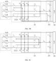
- FIG. 5A to FIG. 5D it can be seen from FIG. 5A to FIG. 5D that, when the current passes through zero, more current flows to an inter-phase switch, and less to the inductor L o at the midpoint and a diode.
- the charging module 100 shown in the embodiments of FIG. 5A to FIG. 5D when the power factor is not 1 (that is, there is a phase difference between the input voltage and the input current), in this application, the inductor is added between the bus midpoint and the three-phase rectifier module in Vienna topology.
- a power factor correction function can be implemented, and there is an effect of improving a bus ripple and a current waveform in a working condition with a non-unity power factor.
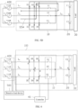
- FIG. 6 is a schematic diagram of a structure of a charging module 100 according to another embodiment of this application.
- a reactive load device 50 may be connected between the input power supply 400 and the three-phase rectifier module 10.
- the charging module shown in FIG. 6 may be used in a scenario of an optical storage charging station.
- the reactive load device 50 may be a capacitive load device or an inductive load device.
- the capacitive load device may be a battery, a computer, or the like.
- the inductive load device may be a transformer, a motor, or the like.
- the central control unit 350 monitors a value of a power factor of an entire system. To ensure that the entire system runs with a unity power factor, there is no phase difference between a sum of the two parts of the current and an output voltage, that is, all electricity obtained from the power grid is active power.
- the controller 40 may control the statuses of the switches S1 to S3 in the three-phase rectifier module 10 based on power factor instruction information delivered by the central control unit 350, to control the phase difference between the input voltage and the input current, so that the charging module works in a working condition with a non-unity power factor. In this way, the phase difference between the input voltage and the input current in the entire system due to a capacitive reactive power can be compensated, thereby increasing the value of the power factor of the entire system.
- the controller 40 may regulate a phase-locked loop for controlling, and translate a current reference signal, so that the input current lags the input voltage, thereby controlling an angle between the input voltage and the input current of the charging module. In this way, the charging module can run with a non-unity power factor, so that the charging module can absorb an inductive reactive power and emit a capacitive reactive power, thereby ensuring that the entire system runs with a unity power factor.
- FIG. 7 is a schematic diagram of a structure of a charging module 100 according to another embodiment of this application.
- the charging module 100 may further include a switch S4.
- the switch S4 is connected in parallel to the inductor L o .
- a first end of the switch S4 may be connected to the controller 40
- a second end of the switch S4 may be connected to the first end of the inductor L o
- the third end of the switch S1, the third end of the switch S2, and the third end of the switch S3 may be connected to the second end of the inductor L o and the midpoint between the bus capacitor C1 and the bus capacitor C2.
- the first end of the switch S4 may be used as a control end of the switch S4. That is, the controller 40 may control a status of the switch S4. For example, the controller 40 may control the switch S4 to be on or off. Optionally, the controller 40 may be in a signal connection to the first end of the switch S4, or the controller 40 may be electrically connected to the first end of the switch S4.
- the switch S4 may be a relay.
- the switch S4 may alternatively be a MOS transistor or a switch component, for example, an IGBT, a SiC transistor, or a GaN transistor.
- the controller 40 may output a control signal to the first end of the switch S4 to control the switch S4 to be on, so that the inductor L o can be in a short-circuit connection.
- the three-phase rectifier module 10 is in conventional Vienna topology, and power conversion from an alternating current to a direct current can be implemented efficiently, thereby improving system efficiency.
- the controller 40 may output a control signal to the first end of the switch S4 to control the switch S4 to be off, so that the inductor L o may be connected between the midpoint O between the bus capacitor C1 and the bus capacitor C2 and the switches S1 to S3.
- a working principle of the charging module is the same as a working principle of the charging module in the embodiment of FIG. 4 .
- the switch S4 is added between the bus midpoint and the switches in Vienna topology. In this way, a status of the switch S4 can be controlled in different charging scenarios, so that charging scenario adaptability of the charging module is extended, and an indicator of the charging module in a normal working condition is not affected.
- an embodiment of this application further provides a charging device 600.
- the charging device 600 may include the charging module 100 described in the foregoing embodiments and a power supply 700.
- the power supply 700 may supply power to the charging module 100. It can be understood that, in some embodiments, the power supply 700 may be the input power supply in the foregoing embodiments.
- the charging device 600 may be, but is not limited to, a direct current charging pile, a vehicle-mounted charger, a high-power charging pile, an ultra-high-power charging pile, a portable charging pile, or the like.
- An embodiment of this application further provides a charging system 800.
- the charging system 800 may include the charging device 600 described in the foregoing embodiment and an electric device 900.
- the charging device 600 may be electrically connected to one or more electric devices 900.
- the charging device 600 may be configured to charge the one or more electric devices 900.
- the charging device 600 may be a charging pile.
- the electric device 900 may be an electric vehicle, an electric bicycle, an electric motorcycle, or the like.
- the charging device 600 is a direct current charging pile, and the electric device 900 is an electric vehicle.
- the direct current charging pile may be electrically connected to one electric vehicle, and charge the electric vehicle.
- the direct current charging pile may be electrically connected to a plurality of electric vehicles, and charge the plurality of electric vehicles simultaneously.
Landscapes
- Engineering & Computer Science (AREA)
- Power Engineering (AREA)
- Transportation (AREA)
- Mechanical Engineering (AREA)
- Rectifiers (AREA)
Abstract
Description
- This application relates to the field of electrical and electronic technologies, and in particular, to a charging module, a charging device, and a charging system.
- Three-phase Vienna rectifier topology is widely used in a charging system scenario with unidirectional transmission of an active power. For example, an active load device and a reactive load device are included in a charging system. To ensure that the system has a unity power factor, an extra reactive apparatus usually needs to be disposed for compensation. Therefore, a reactive power regulation function is designed in the Vienna topology to reduce system costs.
- In a conventional power factor correction solution: 1. A diode in the Vienna topology is replaced with any one of a metal-oxide-semiconductor field-effect transistor (Metal-Oxide-Semiconductor Field-Effect Transistor, MOSFET)/IGBT, a silicon carbide transistor, a gallium nitride transistor, and another power switch transistor. In this way, bidirectional power flow can be implemented, and a power factor correction function can be implemented. However, in this solution, costs are high. 2. Based on the Vienna topology, a compensation range is determined based on an angle of an input voltage, and a common-mode signal is generated and input into a modulating wave, to change a phase difference between a modulating voltage and the input voltage. However, it is complex to implement this solution, and a current waveform is distorted.
- In view of this, this application provides a charging module, a charging device, and a charging system, so that variable power factor performance of unidirectional power flow topology can be as good as that of bidirectional power flow topology. A current waveform and a bus ripple in a working condition with a non-unity power factor can be optimized, and costs can be reduced.
- A first aspect of this application provides a charging module, configured to supply power to a load. The charging module includes a three-phase rectifier module, a bus capacitor module, an inductor, and a controller. An input end of the three-phase rectifier module is electrically connected to an input power supply, where an output end of the three-phase rectifier module is electrically connected to an input end of the bus capacitor module, and the three-phase rectifier module includes a three-phase bridge arm. The bus capacitor module includes a first bus capacitor and a second bus capacitor, where the first bus capacitor is electrically connected between a first output end of the three-phase bridge arm and a midpoint of the three-phase bridge arm, and the second bus capacitor is electrically connected between a second output end of the three-phase bridge arm and the midpoint. The inductor is electrically connected to the midpoint of the three-phase bridge arm and a midpoint between the first bus capacitor and the second bus capacitor. The controller is configured to obtain an input voltage and an input current of the charging module, and is further configured to control a status of the three-phase rectifier module based on the input voltage and the input current.
- In this application, an inductor is added between a bus midpoint and a three-phase rectifier module in Vienna topology. Because there is no sudden change in a current through an inductor, and the inductor may absorb a part of reactive power and isolate the rectifier module from a bus capacitor, not only a power factor correction function can be implemented, but also there is an effect of improving a bus ripple and a current waveform in a working condition with a non-unity power factor.
- In an optional implementation, the three-phase rectifier module includes a first switch, a second switch, and a third switch. The first switch is electrically connected to a midpoint of a first-phase bridge arm and a first end of the inductor, a second end of the inductor is electrically connected to the midpoint between the first bus capacitor and the second bus capacitor, the second switch is electrically connected to a midpoint of a second-phase bridge arm and the first end of the inductor, and the third switch is electrically connected to a midpoint of a third-phase bridge arm and the first end of the inductor.
- In an optional implementation, the controller is configured to: when it is detected that the input current is less than a current threshold, regulate a phase difference between the input current and the input voltage by controlling the first switch, the second switch, and the third switch.
- In an optional implementation, the controller is further configured to: when the input power supply charges a reactive load device, regulate the phase difference betweenthe input current and the input voltage by controlling the first switch, the second switch, and the third switch.
- In an optional implementation, the charging module further includes a fourth switch, the fourth switch is connected in parallel to the inductor, and the fourth switch is further connected to the controller.
- In an optional implementation, the controller is further configured to control the fourth switch to be on when the charging module needs to work with a unity power factor.
- In an optional implementation, the controller is further configured to control the fourth switch to be off when the charging module needs to work with a non-unity power factor.
- A second aspect of this application further provides a charging device, configured to supply power to a load and including an input power supply and a charging module. The input power supply is configured to supply power to the charging module, and the charging module includes a three-phase rectifier module, a bus capacitor module, an inductor, and a controller. An input end of the three-phase rectifier module is electrically connected to an input power supply, where an output end of the three-phase rectifier module is electrically connected to an input end of the bus capacitor module, and the three-phase rectifier module includes a three-phase bridge arm. The bus capacitor module includes a first bus capacitor and a second bus capacitor, where the first bus capacitor is electrically connected between a first output end of the three-phase bridge arm and a midpoint of the three-phase bridge arm, and the second bus capacitor is electrically connected between a second output end of the three-phase bridge arm and the midpoint. The inductor is electrically connected to the midpoint of the three-phase bridge arm and a midpoint between the first bus capacitor and the second bus capacitor. The controller is configured to obtain an input voltage and an input current of the charging module, and is further configured to control a status of the three-phase rectifier module based on the input voltage and the input current.
- In this application, an inductor is added between a bus midpoint and a three-phase rectifier module in Vienna topology. In this application, a power factor correction function can be implemented, and there is an effect of improving a bus ripple and an input current waveform in a working condition with a non-unity power factor.
- In an optional implementation, the three-phase rectifier module includes a first switch, a second switch, and a third switch. The first switch is electrically connected to a midpoint of a first-phase bridge arm and a first end of the inductor, a second end of the inductor is electrically connected to the midpoint between the first bus capacitor and the second bus capacitor, the second switch is electrically connected to a midpoint of a second-phase bridge arm and the first end of the inductor, and the third switch is electrically connected to a midpoint of a third-phase bridge arm and the first end of the inductor.
- In an optional implementation, the charging module further includes a fourth switch, the fourth switch is connected in parallel to the inductor, and the fourth switch is further connected to the controller and a hardware circuit, for example, a peripheral or driver related to the controller. The controller is further configured to: control the fourth switch to be on when the charging module needs to work with a unity power factor; and control the fourth switch to be off when the charging module needs to work with a non-unity power factor.
- According to a third aspect, an embodiment of this application further provides a charging system, including a charging device and one or more electric devices. The charging device is electrically connected to the one or more electric devices to charge the one or more electric devices. The charging device may include an input power supply and a charging module. The input power supply is configured to supply power to the charging module, and the charging module includes a three-phase rectifier module, a bus capacitor module, an inductor, and a controller. An input end of the three-phase rectifier module is electrically connected to an input power supply, where an output end of the three-phase rectifier module is electrically connected to an input end of the bus capacitor module, and the three-phase rectifier module includes a three-phase bridge arm. The bus capacitor module includes a first bus capacitor and a second bus capacitor, where the first bus capacitor is electrically connected between a first output end of the three-phase bridge arm and a midpoint of the three-phase bridge arm, and the second bus capacitor is electrically connected between a second output end of the three-phase bridge arm and the midpoint. The inductor is electrically connected to the midpoint of the three-phase bridge arm and a midpoint between the first bus capacitor and the second bus capacitor. The controller is configured to obtain an input voltage and an input current of the input power supply, and is further configured to control a status of the three-phase rectifier module based on the input voltage and the input current. In the charging system in this application, an inductor may be added between a bus midpoint and a three-phase rectifier module in Vienna topology. Because there is no sudden change in a current through an inductor, and the inductor may absorb a part of reactive power and isolate the rectifier module from a bus capacitor, not only a power factor correction function can be implemented, but also there is an effect of improving a bus ripple and a current waveform in a working condition with a non-unity power factor.
- In embodiments of this application, the inductor is disposed between the three-phase rectifier module and the midpoint of the bus capacitor module, so that the power factor correction function can be implemented, and there is an effect of improving a bus ripple and an input current waveform in a working condition with a non-unity power factor. In this way, variable power factor performance of unidirectional power flow topology can be as good as that of bidirectional power flow topology, thereby reducing hardware costs.
-
-
FIG. 1 is a schematic diagram of an application environment of a charging module according to an embodiment of this application; -
FIG. 2 is a schematic diagram of another application environment of a charging module according to an embodiment of this application; -
FIG. 3 is a schematic diagram of another application environment of a charging module according to an embodiment of this application; -
FIG. 4 is a schematic diagram of a structure of a charging module according to an embodiment of this application; -
FIG. 5A to FIG. 5D are a schematic diagram of a charging module with A-phase zero crossing according to this application; -
FIG. 6 is another schematic diagram of a structure of a charging module according to an embodiment of this application; -
FIG. 7 is another schematic diagram of a structure of a charging module according to an embodiment of this application; -
FIG. 8 is a schematic diagram of a structure of a charging device according to an embodiment of this application; and -
FIG. 9 is a schematic diagram of a structure of a charging system according to an embodiment of this application. - It should be noted that, when an element is considered to be "connected to" another element, the element may be directly connected to the another element, or there may be an element disposed in between. When an element is considered to be "disposed" on another element, it may be directly disposed on the another element, or there may be an element disposed in between.
- Unless otherwise defined, all technical and scientific terms used in this specification have same meanings as those usually understood by a person skilled in the art related to this application. In this specification, the terms used in the description of this application are merely intended to describe specific embodiments, but are not intended to limit this application. The term "and/or" used in this specification includes any and all combinations of one or more related listed items.
- Refer to
FIG. 1. FIG. 1 is a schematic diagram of an environment in which a charging module is used in an optical storage charging system according to an embodiment of this application. - As shown in
FIG. 1 , the optical storage charging system may include a photovoltaicpower generation system 310, anenergy storage system 320, a chargingstation 330, acharging device 340, and acentral control unit 350. The photovoltaicpower generation system 310 may be connected to theenergy storage system 320, the chargingstation 330, and thecharging device 340 through a direct current bus. The photovoltaicpower generation system 310, theenergy storage system 320, the chargingstation 330, and thecharging device 340 exchange information with thecentral control unit 350 through a communication cable or via a communication device. It can be understood that thecentral control unit 350 may be configured to monitor related information, for example, powers of an entire system and each component, and further configured to schedule each power unit. - It can be understood that the photovoltaic
power generation system 310 may include a plurality ofphotovoltaic panel assemblies 312 and a plurality of DC/DC converters 314. The plurality ofphotovoltaic panel assemblies 312 may be connected to the plurality of DC/DC converters 314 in a one-to-one correspondence. It can be understood that thephotovoltaic panel assemblies 312 may be power generation apparatuses that are exposed to sunlight and that generate a direct current. Thephotovoltaic panel assemblies 312 may transmit a generated direct voltage to the DC/DC converters 314, and the DC/DC converters 314 may convert the direct voltage from thephotovoltaic panel assemblies 312. In this way, the DC/DC converters 314 may transmit the direct voltage on which direct current conversion is performed to the direct current bus of the system through a direct current bus. - The charging
device 340 may include aninput power supply 342 and acharging module 100. Theinput power supply 342 may be an alternating current power supply. For example, theinput power supply 342 may output an alternating voltage to thecharging module 100. Thecharging module 100 may be configured to convert the alternating voltage output by theinput power supply 342 into a direct voltage. Thecharging module 100 may further transmit the direct voltage obtained through the conversion to the direct current bus, and a load may get energy from the direct current bus. - The
energy storage system 320 may include a DC/DC converter 322 and a plurality of battery packs 324. The plurality of battery packs 324 are connected to the DC/DC converter 322. In a scenario, the DC/DC converter 322 may receive, through a direct current bus, energy output by the photovoltaicpower generation system 310, to charge the plurality of battery packs 324. In another scenario, the DC/DC converter 322 may receive, through a direct current bus, energy output by the chargingdevice 340, to charge the plurality of battery packs 324. In another scenario, the plurality of battery packs 324 may output a direct voltage to the DC/DC converter 322, and the DC/DC converter 322 may convert the direct voltage output by the plurality of battery packs 324, and output energy to charge the load through a direct current bus. - The charging
station 330 may include a DC/DC converter 332. The DC/DC converter 332 may obtain energy and a power from the direct current bus, to supply power to a plurality ofelectric vehicles 334. - It can be understood that, in this embodiment, the charging
device 340 and the photovoltaicpower generation system 310 may output energy to the direct current bus. Therefore, a load device (for example, the charging station 330) may obtain energy through the direct current bus. Theenergy storage system 320 may output energy to the direct current bus, or theenergy storage system 320 may obtain energy through the direct current bus. For example, during peak electricity hours, theenergy storage system 320 may output energy to the direct current bus, and the load device may obtain, through the direct current bus, the energy output by theenergy storage system 320, to supply power to the load device. During off-peak electricity hours, theenergy storage system 320 may obtain energy through the direct current bus for storing energy. Therefore, theenergy storage system 320 is mainly used for storing energy during off-peak electricity hours and supplying energy during peak electricity hours, so that the entire charging station system maximizes the use of new photovoltaic energy, and consumption of a power grid is reduced. - Refer to
FIG. 2. FIG. 2 is a schematic diagram of another application environment of acharging module 100 according to an embodiment of this application. - In a scenario shown in
FIG. 2 , thecharging module 100 may be configured to charge anelectric vehicle 200 by using an external power supply. It should be noted that, in another embodiment of this application, thecharging module 100 is not limited to being used in theelectric vehicle 200. - For example, the
charging module 100 may be a vehicle-mounted charger in theelectric vehicle 200. An alternatingcurrent power grid 210 may output alternating current electrical energy to an alternating current chargingpile 220. The alternating current chargingpile 220 may output alternating current electrical energy to thecharging module 100. Thecharging module 100 may process or convert the received alternating current electrical energy, and charge abattery 230 in theelectric vehicle 200. - Refer to
FIG. 3. FIG. 3 is a schematic diagram of another application environment of acharging module 100 according to an embodiment of this application. - In a scenario shown in
FIG. 3 , thecharging module 100 may be used in a direct current chargingpile 250. An alternatingcurrent power grid 210 may output alternating current electrical energy to atransformer 240. Thetransformer 240 performs conversion and outputs alternating current electrical energy to the directcurrent charging pile 250. The direct current chargingpile 250 processes or converts the alternating current electrical energy, and charges abattery 230 in anelectric vehicle 200. - It can be understood that, in some possible application scenarios, the
charging module 100 may be used in a direct current charging pile, a vehicle-mounted charger, a high-power charging pile, an ultra-high-power charging pile, a portable charging pile, or the like. - An internal structure of the charging module is described below in detail.
- Refer to
FIG. 4. FIG. 4 is a schematic diagram of a structure of acharging module 100 according to an embodiment of this application. - In this embodiment, the
charging module 100 may be electrically connected to aninput power supply 400. In this embodiment, theinput power supply 400 may be a three-phase alternating current power supply, and may supply power to thecharging module 100. Thecharging module 100 may include a three-phase rectifier module 10, abus capacitor module 20, acontroller 40, and an inductor Lo. - The
bus capacitor module 20 may be electrically connected between the three-phase rectifier module 10 and aload device 30. Thecontroller 40 may be connected to the three-phase rectifier module 10, and thecontroller 40 may control thecharging module 100 to perform AC-DC processing by using the three-phase rectifier module 10 in Vienna topology, and correspondingly control a status of a switch in the three-phase rectifier module 10. - It can be understood that, in this embodiment, the three-
phase rectifier module 10 may be configured to process an output voltage of theinput power supply 400. For example, in a scenario, the three-phase rectifier module 10 may be configured to convert an alternating voltage output by theinput power supply 400 into a direct voltage, and the direct voltage may be used for supplying power to theload device 30. - The three-
phase rectifier module 10 may include a three-phase bridge arm connected in parallel, and the three-phase bridge arm may include a first-phase bridge arm U, a second-phase bridge arm V, and a third-phase bridge arm W. - The first-phase bridge arm U may include a first diode D1 and a second diode D2. The second-phase bridge arm V may include a third diode D3 and a fourth diode D4. The third-phase bridge arm W may include a fifth diode D5 and a sixth diode D6.
- In this embodiment, an anode of the first diode D1 may be electrically connected to a cathode of the second diode D2, a cathode of the first diode D1 may be electrically connected to a cathode of the third diode D3 and a cathode of the fifth diode D5, and an anode of the second diode D2 may be electrically connected to an anode of the fourth diode D4 and an anode of the sixth diode D6. An anode of the third diode D3 may be electrically connected to a cathode of the fourth diode D4. An anode of the fifth diode D5 may be electrically connected to a cathode of the sixth diode D6. The cathode of the fifth diode D5 may be further electrically connected to the
bus capacitor module 20, and the anode of the sixth diode D6 may be further electrically connected to thebus capacitor module 20. - It can be understood that the three-
phase rectifier module 10 in this embodiment may further include a switch S1, a switch S2, and a switch S3. - A first end of the switch S1 may be connected to the
controller 40, a second end of the switch S1 may be electrically connected to a midpoint A between thefirst diode D 1 and the second diode D2, and a third end of the switch S1 may be electrically connected to a third end of the switch S2, a third end of the switch S3, and a first end of the inductor Lo. It can be understood that the first end of theswitch S 1 may be used as a control end of theswitch S 1, that is, thecontroller 40 may control a status of theswitch S 1. For example, thecontroller 40 may control the switch S1 to be on or off. Optionally, thecontroller 40 may be in a signal connection to the first end of the switch S1, or thecontroller 40 may be electrically connected to the first end of the switch S1. - A first end of the switch S2 may be connected to the
controller 40, a second end of the switch S2 may be electrically connected to a midpoint B between the third diode D3 and the fourth diode D4, and a third end of the switch S2 may be electrically connected to the first end of the inductor Lo, the third end of theswitch S 1, and the third end of the switch S3. It can be understood that the first end of the switch S2 may be used as a control end of the switch S2. That is, thecontroller 40 may control a status of the switch S2. For example, thecontroller 40 may control the switch S2 to be on or off. Optionally, thecontroller 40 may be in a signal connection to the first end of the switch S2, or thecontroller 40 may be electrically connected to the first end of the switch S2. - A first end of the switch S3 may be connected to the
controller 40, a second end of the switch S3 may be electrically connected to a midpoint C between the fifth diode D5 and the sixth diode D6, and the third end of the switch S3 may be electrically connected to the first end of the inductor Lo, the third end of theswitch S 1, and the third end of the switch S2. It can be understood that the first end of the switch S3 may be used as a control end of the switch S3. That is, thecontroller 40 may control a status of the switch S3. For example, thecontroller 40 may control the switch S3 to be on or off. Optionally, thecontroller 40 may be in a signal connection to the first end of the switch S3, or thecontroller 40 may be electrically connected to the first end of the switch S3. - It can be understood that, in some optional embodiments, the switches S1 to S3 may each be any one of a metal-oxide-semiconductor field-effect transistor (Metal-Oxide-Semiconductor Field-Effect Transistor, MOSFET) or an insulated gate bipolar transistor (Insulated Gate Bipolar Transistor, IGBT), a silicon carbide transistor, a gallium nitride transistor, and another power switch transistor.
- In this embodiment, the three-
phase rectifier module 10 may further include a first inductor La, a second inductor Lb, and a third inductor Lc. A first end of the first inductor La may be electrically connected to a first output end of theinput power supply 400, and a second end of the first inductor La may be electrically connected to the midpoint A. A first end of the second inductor Lb may be electrically connected to a second output end of theinput power supply 400, and a second end of the second inductor Lb may be electrically connected to the midpoint B. A first end of the third inductor Lc may be electrically connected to a third output end of theinput power supply 400, and a second end of the third inductor Lc may be electrically connected to the midpoint C. - The
bus capacitor module 20 may include a first bus capacitor C1 and a second bus capacitor C2. A first end of the first bus capacitor C1 may be electrically connected to the cathode of thefirst diode D 1, the cathode of the third diode D3, and the cathode of the fifth diode D5, a second end of the first bus capacitor C1 may be electrically connected to a first end of the second bus capacitor C2, and a second end of the second bus capacitor C2 may be electrically connected to the anode of the second diode D2, the anode of the fourth diode D4, and the anode of the sixth diode D6. A second end of the inductor Lo may be electrically connected to a midpoint O between the first bus capacitor C1 and the second bus capacitor C2. - It can be understood that, in this embodiment, the first inductor La, the second inductor Lb, and the third inductor Lc may be configured for energy storage and filtering during on and off of the
switch S 1, the switch S2, and the switch S3. Thebus capacitor module 20 may be configured for energy storage and voltage stabilization of a direct current-side bus. - In the
charging module 100 in this application, the inductor Lo is added between the bus capacitor midpoint and the switches S1 to S3. Based on such a design, the charging module in this application can implement a power factor correction function, and can further optimize a current waveform and a bus ripple in a working condition with a non-unity power factor. In this way, variable power factor performance of unidirectional power flow topology can be as good as that of bidirectional power flow topology, thereby reducing hardware costs. - It can be understood that the
controller 40 in this embodiment may obtain an input voltage and an input current of the charging module. Thecontroller 40 may be configured to control the statuses of the switches S1 to S3 in thecharging module 100. - In an embodiment shown in
FIG. 4 , when a voltage of a power grid needs to be regulated, thecharging module 100 may be used for regulating a reactive power of the power grid for reactive power compensation, to achieve reactive power voltage regulation. - In another scenario, when the
charging module 100 is used in a working condition with a light load, a bus capacitor of thecharging module 100 is large, and there is a large X-capacitor on an input side. As a result, in the working condition with the light load of the charging module, an input current leads an input voltage by an angle (for example, 1 degree to 5 degrees), and a value of a power factor of thecharging module 100 in the working condition with the light load is low. In this application scenario, thecontroller 40 may control the input current to lag the input voltage by using a phase-locked loop, to compensate for a phase difference between the input voltage and the input current caused by a capacitive reactive power, thereby increasing the value of the power factor of thecharging module 100. - It can be understood that, because Vienna topology is unidirectional power flow topology, when there is a phase difference between an input voltage and an input current, a zero-crossing distortion of a current occurs. In this application, the inductor Lo may be added between a bus midpoint and a switch in the Vienna topology. Because there is no sudden change in a current through the inductor Lo, when the current passes through zero, more current flows to an inter-phase switch, and less to the inductor Lo at the midpoint and a diode. In this way, a waveform when the current passes through zero is optimized. Based on such a design, the inductor Lo may isolate a voltage at the bus midpoint from a voltage of the inductor, and the inductor may further absorb a part of reactive power. In this way, a bus voltage ripple can be further attenuated, and a bus ripple can be reduced.
- An example of A-phase current zero crossing is used below for description. A B-phase current is a reverse current, and a C-phase current is a forward current.
- As shown in
FIG. 5A , thecontroller 40 may control the switch S1 and the switch S3 to be on and the switch S2 to be off. In this case, a current of theinput power supply 400 may flow through an A-phase loop and a C-phase loop. A current path of theinput power supply 400 is shown as a path S51 inFIG. 5A . - As shown in
FIG. 5B , thecontroller 40 may control the switch S3 to be on and the switch S1 and the switch S2 to be off. In this case, the current of theinput power supply 400 may flow through the inductor Lo and the bus capacitor C2. The current path of theinput power supply 400 is shown as a path S52 inFIG. 5B . - As shown in
FIG. 5C , thecontroller 40 may control the switch S1, the switch S2, and the switch S3 to be on. In this case, the current of theinput power supply 400 may flow through an A-phase loop, the B-phase loop, and the C-phase loop. The current path of theinput power supply 400 is shown as a path S53 inFIG. 5C . - As shown in
FIG. 5D , thecontroller 40 may control the switch S1 and the switch S2 to be on and the switch S3 to be off. In this case, the current of theinput power supply 400 may flow through the inductor Lo, the bus capacitor C1, the A-phase loop, and the B-phase loop. The current path of theinput power supply 400 is shown as a path S54 inFIG. 5D . - It can be seen from
FIG. 5A to FIG. 5D that, when the current passes through zero, more current flows to an inter-phase switch, and less to the inductor Lo at the midpoint and a diode. By using thecharging module 100 shown in the embodiments ofFIG. 5A to FIG. 5D , when the power factor is not 1 (that is, there is a phase difference between the input voltage and the input current), in this application, the inductor is added between the bus midpoint and the three-phase rectifier module in Vienna topology. Because there is no sudden change in a current through the inductor, and the inductor may absorb a part of reactive power and isolate the three-phase rectifier module from the bus capacitor, a power factor correction function can be implemented, and there is an effect of improving a bus ripple and a current waveform in a working condition with a non-unity power factor. - Refer to
FIG. 6. FIG. 6 is a schematic diagram of a structure of acharging module 100 according to another embodiment of this application. - A difference from the
charging module 100 shown in the embodiment ofFIG. 4 is that, in this embodiment, as shown inFIG. 6 , a reactive load device 50 may be connected between theinput power supply 400 and the three-phase rectifier module 10. - It can be understood that the charging module shown in
FIG. 6 may be used in a scenario of an optical storage charging station. The reactive load device 50 may be a capacitive load device or an inductive load device. For example, the capacitive load device may be a battery, a computer, or the like. The inductive load device may be a transformer, a motor, or the like. - When the
input power supply 400 charges the reactive load device 50 (for example, the capacitive load device or the inductive load device), one part of an input current flows through the reactive load device 50, and the other part of the input current flows through thecharging module 100. In this application scenario, thecentral control unit 350 monitors a value of a power factor of an entire system. To ensure that the entire system runs with a unity power factor, there is no phase difference between a sum of the two parts of the current and an output voltage, that is, all electricity obtained from the power grid is active power. In this case, thecontroller 40 may control the statuses of the switches S1 to S3 in the three-phase rectifier module 10 based on power factor instruction information delivered by thecentral control unit 350, to control the phase difference between the input voltage and the input current, so that the charging module works in a working condition with a non-unity power factor. In this way, the phase difference between the input voltage and the input current in the entire system due to a capacitive reactive power can be compensated, thereby increasing the value of the power factor of the entire system. In an optional implementation, thecontroller 40 may regulate a phase-locked loop for controlling, and translate a current reference signal, so that the input current lags the input voltage, thereby controlling an angle between the input voltage and the input current of the charging module. In this way, the charging module can run with a non-unity power factor, so that the charging module can absorb an inductive reactive power and emit a capacitive reactive power, thereby ensuring that the entire system runs with a unity power factor. - Refer to
FIG. 7. FIG. 7 is a schematic diagram of a structure of acharging module 100 according to another embodiment of this application. - A difference from the
charging module 100 shown in the embodiment ofFIG. 4 is that, in this embodiment, as shown inFIG. 7 , thecharging module 100 may further include a switch S4. - In this embodiment, the switch S4 is connected in parallel to the inductor Lo. Specifically, a first end of the switch S4 may be connected to the
controller 40, a second end of the switch S4 may be connected to the first end of the inductor Lo, the third end of the switch S1, the third end of the switch S2, and the third end of the switch S3, and the third end of the switch S4 may be connected to the second end of the inductor Lo and the midpoint between the bus capacitor C1 and the bus capacitor C2. - It can be understood that the first end of the switch S4 may be used as a control end of the switch S4. That is, the
controller 40 may control a status of the switch S4. For example, thecontroller 40 may control the switch S4 to be on or off. Optionally, thecontroller 40 may be in a signal connection to the first end of the switch S4, or thecontroller 40 may be electrically connected to the first end of the switch S4. - In an optional implementation, the switch S4 may be a relay. The switch S4 may alternatively be a MOS transistor or a switch component, for example, an IGBT, a SiC transistor, or a GaN transistor.
- In an application scenario, when the
charging module 100 needs to work with a unity power factor, thecontroller 40 may output a control signal to the first end of the switch S4 to control the switch S4 to be on, so that the inductor Lo can be in a short-circuit connection. In this case, the three-phase rectifier module 10 is in conventional Vienna topology, and power conversion from an alternating current to a direct current can be implemented efficiently, thereby improving system efficiency. - In another application scenario, when the
charging module 100 needs to work with a non-unity power factor, thecontroller 40 may output a control signal to the first end of the switch S4 to control the switch S4 to be off, so that the inductor Lo may be connected between the midpoint O between the bus capacitor C1 and the bus capacitor C2 and the switches S1 to S3. In this case, a working principle of the charging module is the same as a working principle of the charging module in the embodiment ofFIG. 4 . - Based on the embodiment shown in
FIG. 7 , in this application, the switch S4 is added between the bus midpoint and the switches in Vienna topology. In this way, a status of the switch S4 can be controlled in different charging scenarios, so that charging scenario adaptability of the charging module is extended, and an indicator of the charging module in a normal working condition is not affected. - It can be understood that, as shown in
FIG. 8 , an embodiment of this application further provides acharging device 600. The chargingdevice 600 may include thecharging module 100 described in the foregoing embodiments and apower supply 700. Thepower supply 700 may supply power to thecharging module 100. It can be understood that, in some embodiments, thepower supply 700 may be the input power supply in the foregoing embodiments. - In some possible application scenarios, the charging
device 600 may be, but is not limited to, a direct current charging pile, a vehicle-mounted charger, a high-power charging pile, an ultra-high-power charging pile, a portable charging pile, or the like. - Refer to
FIG. 9 . An embodiment of this application further provides acharging system 800. Thecharging system 800 may include thecharging device 600 described in the foregoing embodiment and anelectric device 900. - It can be understood that the
charging device 600 may be electrically connected to one or moreelectric devices 900. The chargingdevice 600 may be configured to charge the one or moreelectric devices 900. - In some embodiments, the charging
device 600 may be a charging pile. Theelectric device 900 may be an electric vehicle, an electric bicycle, an electric motorcycle, or the like. For example, in some application scenarios, the chargingdevice 600 is a direct current charging pile, and theelectric device 900 is an electric vehicle. The direct current charging pile may be electrically connected to one electric vehicle, and charge the electric vehicle. In another possible scenario, the direct current charging pile may be electrically connected to a plurality of electric vehicles, and charge the plurality of electric vehicles simultaneously. - The foregoing descriptions are merely examples of implementations of this application, but are not any form of limitations on this application. Although this application has been disclosed as examples of implementations as described above, but the implementations are not intended to limit this application, and any person skilled in the art may make some changes or modifications to the technical content disclosed above as equivalent implementations of equivalent variations without departing from the scope of the technical solutions of this application. Any simple changes, equivalent variations, or modifications made to the foregoing implementations according to the technical essence of this application without departing from the content of the technical solutions of this application shall fall within the scope of the technical solutions of this application.
Claims (9)
- A charging module, configured to supply power to a load, wherein the charging module comprises a three-phase rectifier module, a bus capacitor module, an inductor, and a controller;an input end of the three-phase rectifier module is electrically connected to an input power supply, an output end of the three-phase rectifier module is electrically connected to an input end of the bus capacitor module, and the three-phase rectifier module comprises a three-phase bridge arm;the bus capacitor module comprises a first bus capacitor and a second bus capacitor, the first bus capacitor is electrically connected between a first output end of the three-phase bridge arm and a midpoint of the three-phase bridge arm, and the second bus capacitor is electrically connected between a second output end of the three-phase bridge arm and the midpoint;the inductor is electrically connected to the midpoint of the three-phase bridge arm and a midpoint between the first bus capacitor and the second bus capacitor; andthe controller is configured to obtain an input voltage and an input current of the charging module, and is further configured to control a status of the three-phase rectifier module based on the input voltage and the input current, to control a phase difference between the input voltage and the input current.
- The charging module according to claim 1, whereinthe three-phase rectifier module comprises a first switch, a second switch, and a third switch; andthe first switch is electrically connected to a midpoint of a first-phase bridge arm and a first end of the inductor, a second end of the inductor is electrically connected to the midpoint between the first bus capacitor and the second bus capacitor, the second switch is electrically connected to a midpoint of a second-phase bridge arm and the first end of the inductor, and the third switch is electrically connected to a midpoint of a third-phase bridge arm and the first end of the inductor.
- The charging module according to claim 2, wherein
the controller is configured to: when it is detected that the input current is less than a current threshold, control the phase difference between the input current and the input voltage by controlling the first switch, the second switch, and the third switch. - The charging module according to claim 2 or 3, wherein
the controller is further configured to: when the input power supply charges a capacitive load device or an inductive load device, control the phase difference between the input current and the input voltage by controlling the first switch, the second switch, and the third switch. - The charging module according to any one of claims 1 to 4, wherein
the charging module further comprises a fourth switch, the fourth switch is connected in parallel to the inductor, and the fourth switch is further connected to the controller. - The charging module according to claim 5, wherein
the controller is further configured to control the fourth switch to be on when the charging module needs to work with a unity power factor. - The charging module according to claim 5 or 6, wherein
the controller is further configured to control the fourth switch to be off when the charging module needs to work with a non-unity power factor. - A charging device, configured to supply power to a load and comprising an input power supply and the charging module according to any one of claims 1 to 7, wherein the input power supply is configured to supply power to the charging module.
- A charging system, comprising a charging device and one or more electric devices, wherein the charging device is electrically connected to the one or more electric devices to charge the one or more electric devices, the charging device comprises an input power supply and the charging module according to any one of claims 1 to 7, the input power supply is configured to supply power to the charging module.
Applications Claiming Priority (1)
| Application Number | Priority Date | Filing Date | Title |
|---|---|---|---|
| CN202211288016.8A CN116031988A (en) | 2022-10-20 | 2022-10-20 | Charging modules, charging equipment and charging systems |
Publications (2)
| Publication Number | Publication Date |
|---|---|
| EP4358358A1 true EP4358358A1 (en) | 2024-04-24 |
| EP4358358B1 EP4358358B1 (en) | 2025-11-05 |
Family
ID=86080340
Family Applications (1)
| Application Number | Title | Priority Date | Filing Date |
|---|---|---|---|
| EP23204099.8A Active EP4358358B1 (en) | 2022-10-20 | 2023-10-17 | Charging module, charging device, and charging system |
Country Status (3)
| Country | Link |
|---|---|
| US (1) | US12512752B2 (en) |
| EP (1) | EP4358358B1 (en) |
| CN (1) | CN116031988A (en) |
Citations (1)
| Publication number | Priority date | Publication date | Assignee | Title |
|---|---|---|---|---|
| US20220224250A1 (en) * | 2019-10-02 | 2022-07-14 | HELLA GmbH & Co. KGaA | Bidirectional power converter having intermediate circuit |
Family Cites Families (2)
| Publication number | Priority date | Publication date | Assignee | Title |
|---|---|---|---|---|
| NL2025505B1 (en) * | 2020-05-04 | 2021-11-18 | Prodrive Tech Bv | Electrical power converter |
| CN213027811U (en) | 2020-07-24 | 2021-04-20 | 上海万暨电子科技有限公司 | Single-phase staggered and three-phase Vienna topology compatible input PFC device |
-
2022
- 2022-10-20 CN CN202211288016.8A patent/CN116031988A/en active Pending
-
2023
- 2023-10-17 EP EP23204099.8A patent/EP4358358B1/en active Active
- 2023-10-18 US US18/489,268 patent/US12512752B2/en active Active
Patent Citations (1)
| Publication number | Priority date | Publication date | Assignee | Title |
|---|---|---|---|---|
| US20220224250A1 (en) * | 2019-10-02 | 2022-07-14 | HELLA GmbH & Co. KGaA | Bidirectional power converter having intermediate circuit |
Non-Patent Citations (3)
| Title |
|---|
| AKSSAS ATMANE ET AL: "Bidirectional On-Board charger based on the efficient topology Vienna Rectifier", 2022 2ND INTERNATIONAL CONFERENCE ON INNOVATIVE RESEARCH IN APPLIED SCIENCE, ENGINEERING AND TECHNOLOGY (IRASET), IEEE, 3 March 2022 (2022-03-03), pages 1 - 6, XP034105856, DOI: 10.1109/IRASET52964.2022.9737782 * |
| HARTMANN M ET AL: "Active three-phase rectifier system using a Flying Converter Cell", ENERGY CONFERENCE AND EXHIBITION (ENERGYCON), 2012 IEEE INTERNATIONAL, IEEE, 9 September 2012 (2012-09-09), pages 82 - 89, XP032466788, ISBN: 978-1-4673-1453-4, DOI: 10.1109/ENERGYCON.2012.6348267 * |
| SITHARA S G ACHARIGE ET AL: "Review of Electric Vehicle Charging Technologies, Configurations, and Architectures", ARXIV.ORG, CORNELL UNIVERSITY LIBRARY, 201 OLIN LIBRARY CORNELL UNIVERSITY ITHACA, NY 14853, 30 September 2022 (2022-09-30), pages 1 - 36, XP091331035 * |
Also Published As
| Publication number | Publication date |
|---|---|
| US20240235416A9 (en) | 2024-07-11 |
| EP4358358B1 (en) | 2025-11-05 |
| US20240136939A1 (en) | 2024-04-25 |
| US12512752B2 (en) | 2025-12-30 |
| CN116031988A (en) | 2023-04-28 |
Similar Documents
| Publication | Publication Date | Title |
|---|---|---|
| US10523112B2 (en) | Power converter and method of controlling the same | |
| US20120025609A1 (en) | Very high efficiency uninterruptible power supply | |
| WO2024032463A1 (en) | Dc/dc converter, method for controlling output voltage thereof, and energy storage system | |
| US20250167681A1 (en) | Power conversion apparatus, control method, and power supply system | |
| EP4068610B1 (en) | Converter and on-board charger | |
| Bhowmick et al. | Design and analysis of the low device stress active power decoupling for single-phase grid connection for a wide range of power factor | |
| CN110137977B (en) | Converter station series connection adjusting system and control method | |
| US20240333135A1 (en) | Inverter apparatus and control method thereof | |
| US12580493B2 (en) | Neutral point clamped inverter and photovoltaic power supply system | |
| EE202100018A (en) | A power electronic device for converting alternating current used as input to direct current | |
| CN115241926A (en) | Bus voltage control method, bus balance control method and system thereof | |
| EP3975411B1 (en) | Rectifier, charging system and electric vehicle | |
| EP4358358A1 (en) | Charging module, charging device, and charging system | |
| US20260025088A1 (en) | Single-phase, three-level, buck-boost inverter | |
| CN114915186A (en) | Power unit, control method of power unit, storage medium and high-voltage frequency converter | |
| CN102522813A (en) | Photovoltaic power generation voltage stabilizer | |
| RU2388136C2 (en) | Method for control of power and design of resistance converter for ac electric machines | |
| CN115333434B (en) | A power double compensation switched reluctance motor drive system and control method | |
| EP4523319B1 (en) | Single-phase, three-level, buck-boost inverter | |
| CN224037141U (en) | Uninterruptible power supply | |
| US20260031698A1 (en) | Motor power source regulation circuit, control method and electronic device | |
| US20240424936A1 (en) | Power conversion device and control method thereof, and electric vehicle charging system | |
| US20240195178A1 (en) | Power conversion device and control method thereof | |
| Munendhar et al. | A Power Quality Improved EV Charger With Bridges CUK Converter | |
| Suresh et al. | Role of Power Converters in Renewable Energy Systems: Grid Integration, Control, and Optimization |
Legal Events
| Date | Code | Title | Description |
|---|---|---|---|
| PUAI | Public reference made under article 153(3) epc to a published international application that has entered the european phase |
Free format text: ORIGINAL CODE: 0009012 |
|
| STAA | Information on the status of an ep patent application or granted ep patent |
Free format text: STATUS: THE APPLICATION HAS BEEN PUBLISHED |
|
| AK | Designated contracting states |
Kind code of ref document: A1 Designated state(s): AL AT BE BG CH CY CZ DE DK EE ES FI FR GB GR HR HU IE IS IT LI LT LU LV MC ME MK MT NL NO PL PT RO RS SE SI SK SM TR |
|
| STAA | Information on the status of an ep patent application or granted ep patent |
Free format text: STATUS: REQUEST FOR EXAMINATION WAS MADE |
|
| 17P | Request for examination filed |
Effective date: 20241024 |
|
| RBV | Designated contracting states (corrected) |
Designated state(s): AL AT BE BG CH CY CZ DE DK EE ES FI FR GB GR HR HU IE IS IT LI LT LU LV MC ME MK MT NL NO PL PT RO RS SE SI SK SM TR |
|
| STAA | Information on the status of an ep patent application or granted ep patent |
Free format text: STATUS: EXAMINATION IS IN PROGRESS |
|
| 17Q | First examination report despatched |
Effective date: 20250219 |
|
| GRAP | Despatch of communication of intention to grant a patent |
Free format text: ORIGINAL CODE: EPIDOSNIGR1 |
|
| STAA | Information on the status of an ep patent application or granted ep patent |
Free format text: STATUS: GRANT OF PATENT IS INTENDED |
|
| INTG | Intention to grant announced |
Effective date: 20250612 |
|
| GRAS | Grant fee paid |
Free format text: ORIGINAL CODE: EPIDOSNIGR3 |
|
| GRAA | (expected) grant |
Free format text: ORIGINAL CODE: 0009210 |
|
| STAA | Information on the status of an ep patent application or granted ep patent |
Free format text: STATUS: THE PATENT HAS BEEN GRANTED |
|
| P01 | Opt-out of the competence of the unified patent court (upc) registered |
Free format text: CASE NUMBER: UPC_APP_5369_4358358/2025 Effective date: 20250829 |
|
| AK | Designated contracting states |
Kind code of ref document: B1 Designated state(s): AL AT BE BG CH CY CZ DE DK EE ES FI FR GB GR HR HU IE IS IT LI LT LU LV MC ME MK MT NL NO PL PT RO RS SE SI SK SM TR |
|
| REG | Reference to a national code |
Ref country code: CH Ref legal event code: F10 Free format text: ST27 STATUS EVENT CODE: U-0-0-F10-F00 (AS PROVIDED BY THE NATIONAL OFFICE) Effective date: 20251105 Ref country code: GB Ref legal event code: FG4D |
|
| REG | Reference to a national code |
Ref country code: DE Ref legal event code: R096 Ref document number: 602023008276 Country of ref document: DE |
|
| REG | Reference to a national code |
Ref country code: IE Ref legal event code: FG4D |
|
| REG | Reference to a national code |
Ref country code: NL Ref legal event code: MP Effective date: 20251105 |
|
| PG25 | Lapsed in a contracting state [announced via postgrant information from national office to epo] |
Ref country code: ES Free format text: LAPSE BECAUSE OF FAILURE TO SUBMIT A TRANSLATION OF THE DESCRIPTION OR TO PAY THE FEE WITHIN THE PRESCRIBED TIME-LIMIT Effective date: 20251105 |
|
| REG | Reference to a national code |
Ref country code: LT Ref legal event code: MG9D |
|
| PG25 | Lapsed in a contracting state [announced via postgrant information from national office to epo] |
Ref country code: NO Free format text: LAPSE BECAUSE OF FAILURE TO SUBMIT A TRANSLATION OF THE DESCRIPTION OR TO PAY THE FEE WITHIN THE PRESCRIBED TIME-LIMIT Effective date: 20260205 |
|
| PG25 | Lapsed in a contracting state [announced via postgrant information from national office to epo] |
Ref country code: FI Free format text: LAPSE BECAUSE OF FAILURE TO SUBMIT A TRANSLATION OF THE DESCRIPTION OR TO PAY THE FEE WITHIN THE PRESCRIBED TIME-LIMIT Effective date: 20251105 Ref country code: AT Free format text: LAPSE BECAUSE OF FAILURE TO SUBMIT A TRANSLATION OF THE DESCRIPTION OR TO PAY THE FEE WITHIN THE PRESCRIBED TIME-LIMIT Effective date: 20251105 Ref country code: HR Free format text: LAPSE BECAUSE OF FAILURE TO SUBMIT A TRANSLATION OF THE DESCRIPTION OR TO PAY THE FEE WITHIN THE PRESCRIBED TIME-LIMIT Effective date: 20251105 |
|
| REG | Reference to a national code |
Ref country code: AT Ref legal event code: MK05 Ref document number: 1855465 Country of ref document: AT Kind code of ref document: T Effective date: 20251105 |
|
| PG25 | Lapsed in a contracting state [announced via postgrant information from national office to epo] |
Ref country code: NL Free format text: LAPSE BECAUSE OF FAILURE TO SUBMIT A TRANSLATION OF THE DESCRIPTION OR TO PAY THE FEE WITHIN THE PRESCRIBED TIME-LIMIT Effective date: 20251105 |
|
| PG25 | Lapsed in a contracting state [announced via postgrant information from national office to epo] |
Ref country code: RS Free format text: LAPSE BECAUSE OF FAILURE TO SUBMIT A TRANSLATION OF THE DESCRIPTION OR TO PAY THE FEE WITHIN THE PRESCRIBED TIME-LIMIT Effective date: 20260205 |
|
| PG25 | Lapsed in a contracting state [announced via postgrant information from national office to epo] |
Ref country code: IS Free format text: LAPSE BECAUSE OF FAILURE TO SUBMIT A TRANSLATION OF THE DESCRIPTION OR TO PAY THE FEE WITHIN THE PRESCRIBED TIME-LIMIT Effective date: 20260305 |
|
| PG25 | Lapsed in a contracting state [announced via postgrant information from national office to epo] |
Ref country code: PT Free format text: LAPSE BECAUSE OF FAILURE TO SUBMIT A TRANSLATION OF THE DESCRIPTION OR TO PAY THE FEE WITHIN THE PRESCRIBED TIME-LIMIT Effective date: 20260305 |
|
| PG25 | Lapsed in a contracting state [announced via postgrant information from national office to epo] |
Ref country code: PL Free format text: LAPSE BECAUSE OF FAILURE TO SUBMIT A TRANSLATION OF THE DESCRIPTION OR TO PAY THE FEE WITHIN THE PRESCRIBED TIME-LIMIT Effective date: 20251105 |
|
| PG25 | Lapsed in a contracting state [announced via postgrant information from national office to epo] |
Ref country code: LV Free format text: LAPSE BECAUSE OF FAILURE TO SUBMIT A TRANSLATION OF THE DESCRIPTION OR TO PAY THE FEE WITHIN THE PRESCRIBED TIME-LIMIT Effective date: 20251105 |