EP4358124A1 - Device with laterally graded channel region - Google Patents
Device with laterally graded channel region Download PDFInfo
- Publication number
- EP4358124A1 EP4358124A1 EP23195573.3A EP23195573A EP4358124A1 EP 4358124 A1 EP4358124 A1 EP 4358124A1 EP 23195573 A EP23195573 A EP 23195573A EP 4358124 A1 EP4358124 A1 EP 4358124A1
- Authority
- EP
- European Patent Office
- Prior art keywords
- channel region
- region
- pfet
- csige
- laterally graded
- Prior art date
- Legal status (The legal status is an assumption and is not a legal conclusion. Google has not performed a legal analysis and makes no representation as to the accuracy of the status listed.)
- Pending
Links
Images

Classifications
-
- H—ELECTRICITY
- H10—SEMICONDUCTOR DEVICES; ELECTRIC SOLID-STATE DEVICES NOT OTHERWISE PROVIDED FOR
- H10D—INORGANIC ELECTRIC SEMICONDUCTOR DEVICES
- H10D84/00—Integrated devices formed in or on semiconductor substrates that comprise only semiconducting layers, e.g. on Si wafers or on GaAs-on-Si wafers
- H10D84/80—Integrated devices formed in or on semiconductor substrates that comprise only semiconducting layers, e.g. on Si wafers or on GaAs-on-Si wafers characterised by the integration of at least one component covered by groups H10D12/00 or H10D30/00, e.g. integration of IGFETs
- H10D84/82—Integrated devices formed in or on semiconductor substrates that comprise only semiconducting layers, e.g. on Si wafers or on GaAs-on-Si wafers characterised by the integration of at least one component covered by groups H10D12/00 or H10D30/00, e.g. integration of IGFETs of only field-effect components
- H10D84/83—Integrated devices formed in or on semiconductor substrates that comprise only semiconducting layers, e.g. on Si wafers or on GaAs-on-Si wafers characterised by the integration of at least one component covered by groups H10D12/00 or H10D30/00, e.g. integration of IGFETs of only field-effect components of only insulated-gate FETs [IGFET]
- H10D84/85—Complementary IGFETs, e.g. CMOS
-
- H—ELECTRICITY
- H10—SEMICONDUCTOR DEVICES; ELECTRIC SOLID-STATE DEVICES NOT OTHERWISE PROVIDED FOR
- H10D—INORGANIC ELECTRIC SEMICONDUCTOR DEVICES
- H10D30/00—Field-effect transistors [FET]
- H10D30/60—Insulated-gate field-effect transistors [IGFET]
- H10D30/751—Insulated-gate field-effect transistors [IGFET] having composition variations in the channel regions
-
- H—ELECTRICITY
- H10—SEMICONDUCTOR DEVICES; ELECTRIC SOLID-STATE DEVICES NOT OTHERWISE PROVIDED FOR
- H10D—INORGANIC ELECTRIC SEMICONDUCTOR DEVICES
- H10D62/00—Semiconductor bodies, or regions thereof, of devices having potential barriers
- H10D62/80—Semiconductor bodies, or regions thereof, of devices having potential barriers characterised by the materials
- H10D62/83—Semiconductor bodies, or regions thereof, of devices having potential barriers characterised by the materials being Group IV materials, e.g. B-doped Si or undoped Ge
-
- H—ELECTRICITY
- H10—SEMICONDUCTOR DEVICES; ELECTRIC SOLID-STATE DEVICES NOT OTHERWISE PROVIDED FOR
- H10D—INORGANIC ELECTRIC SEMICONDUCTOR DEVICES
- H10D84/00—Integrated devices formed in or on semiconductor substrates that comprise only semiconducting layers, e.g. on Si wafers or on GaAs-on-Si wafers
- H10D84/01—Manufacture or treatment
- H10D84/0123—Integrating together multiple components covered by H10D12/00 or H10D30/00, e.g. integrating multiple IGBTs
- H10D84/0126—Integrating together multiple components covered by H10D12/00 or H10D30/00, e.g. integrating multiple IGBTs the components including insulated gates, e.g. IGFETs
- H10D84/0165—Integrating together multiple components covered by H10D12/00 or H10D30/00, e.g. integrating multiple IGBTs the components including insulated gates, e.g. IGFETs the components including complementary IGFETs, e.g. CMOS devices
- H10D84/0167—Manufacturing their channels
-
- H—ELECTRICITY
- H10—SEMICONDUCTOR DEVICES; ELECTRIC SOLID-STATE DEVICES NOT OTHERWISE PROVIDED FOR
- H10D—INORGANIC ELECTRIC SEMICONDUCTOR DEVICES
- H10D84/00—Integrated devices formed in or on semiconductor substrates that comprise only semiconducting layers, e.g. on Si wafers or on GaAs-on-Si wafers
- H10D84/01—Manufacture or treatment
- H10D84/0123—Integrating together multiple components covered by H10D12/00 or H10D30/00, e.g. integrating multiple IGBTs
- H10D84/0126—Integrating together multiple components covered by H10D12/00 or H10D30/00, e.g. integrating multiple IGBTs the components including insulated gates, e.g. IGFETs
- H10D84/0165—Integrating together multiple components covered by H10D12/00 or H10D30/00, e.g. integrating multiple IGBTs the components including insulated gates, e.g. IGFETs the components including complementary IGFETs, e.g. CMOS devices
- H10D84/0188—Manufacturing their isolation regions
-
- H—ELECTRICITY
- H10—SEMICONDUCTOR DEVICES; ELECTRIC SOLID-STATE DEVICES NOT OTHERWISE PROVIDED FOR
- H10D—INORGANIC ELECTRIC SEMICONDUCTOR DEVICES
- H10D84/00—Integrated devices formed in or on semiconductor substrates that comprise only semiconducting layers, e.g. on Si wafers or on GaAs-on-Si wafers
- H10D84/01—Manufacture or treatment
- H10D84/02—Manufacture or treatment characterised by using material-based technologies
- H10D84/03—Manufacture or treatment characterised by using material-based technologies using Group IV technology, e.g. silicon technology or silicon-carbide [SiC] technology
- H10D84/038—Manufacture or treatment characterised by using material-based technologies using Group IV technology, e.g. silicon technology or silicon-carbide [SiC] technology using silicon technology, e.g. SiGe
-
- H—ELECTRICITY
- H10—SEMICONDUCTOR DEVICES; ELECTRIC SOLID-STATE DEVICES NOT OTHERWISE PROVIDED FOR
- H10D—INORGANIC ELECTRIC SEMICONDUCTOR DEVICES
- H10D86/00—Integrated devices formed in or on insulating or conducting substrates, e.g. formed in silicon-on-insulator [SOI] substrates or on stainless steel or glass substrates
- H10D86/01—Manufacture or treatment
-
- H—ELECTRICITY
- H10—SEMICONDUCTOR DEVICES; ELECTRIC SOLID-STATE DEVICES NOT OTHERWISE PROVIDED FOR
- H10D—INORGANIC ELECTRIC SEMICONDUCTOR DEVICES
- H10D86/00—Integrated devices formed in or on insulating or conducting substrates, e.g. formed in silicon-on-insulator [SOI] substrates or on stainless steel or glass substrates
- H10D86/201—Integrated devices formed in or on insulating or conducting substrates, e.g. formed in silicon-on-insulator [SOI] substrates or on stainless steel or glass substrates the substrates comprising an insulating layer on a semiconductor body, e.g. SOI
-
- H—ELECTRICITY
- H10—SEMICONDUCTOR DEVICES; ELECTRIC SOLID-STATE DEVICES NOT OTHERWISE PROVIDED FOR
- H10D—INORGANIC ELECTRIC SEMICONDUCTOR DEVICES
- H10D89/00—Aspects of integrated devices not covered by groups H10D84/00 - H10D88/00
- H10D89/60—Integrated devices comprising arrangements for electrical or thermal protection, e.g. protection circuits against electrostatic discharge [ESD]
- H10D89/601—Integrated devices comprising arrangements for electrical or thermal protection, e.g. protection circuits against electrostatic discharge [ESD] for devices having insulated gate electrodes, e.g. for IGFETs or IGBTs
-
- H—ELECTRICITY
- H10—SEMICONDUCTOR DEVICES; ELECTRIC SOLID-STATE DEVICES NOT OTHERWISE PROVIDED FOR
- H10P—GENERIC PROCESSES OR APPARATUS FOR THE MANUFACTURE OR TREATMENT OF DEVICES COVERED BY CLASS H10
- H10P90/00—Preparation of wafers not covered by a single main group of this subclass, e.g. wafer reinforcement
- H10P90/19—Preparing inhomogeneous wafers
- H10P90/1904—Preparing vertically inhomogeneous wafers
- H10P90/1906—Preparing SOI wafers
-
- H—ELECTRICITY
- H10—SEMICONDUCTOR DEVICES; ELECTRIC SOLID-STATE DEVICES NOT OTHERWISE PROVIDED FOR
- H10P—GENERIC PROCESSES OR APPARATUS FOR THE MANUFACTURE OR TREATMENT OF DEVICES COVERED BY CLASS H10
- H10P90/00—Preparation of wafers not covered by a single main group of this subclass, e.g. wafer reinforcement
- H10P90/19—Preparing inhomogeneous wafers
- H10P90/1904—Preparing vertically inhomogeneous wafers
- H10P90/1906—Preparing SOI wafers
- H10P90/1908—Preparing SOI wafers using silicon implanted buried insulating layers, e.g. oxide layers [SIMOX]
-
- H—ELECTRICITY
- H10—SEMICONDUCTOR DEVICES; ELECTRIC SOLID-STATE DEVICES NOT OTHERWISE PROVIDED FOR
- H10W—GENERIC PACKAGES, INTERCONNECTIONS, CONNECTORS OR OTHER CONSTRUCTIONAL DETAILS OF DEVICES COVERED BY CLASS H10
- H10W10/00—Isolation regions in semiconductor bodies between components of integrated devices
- H10W10/01—Manufacture or treatment
- H10W10/011—Manufacture or treatment of isolation regions comprising dielectric materials
- H10W10/014—Manufacture or treatment of isolation regions comprising dielectric materials using trench refilling with dielectric materials, e.g. shallow trench isolations
-
- H—ELECTRICITY
- H10—SEMICONDUCTOR DEVICES; ELECTRIC SOLID-STATE DEVICES NOT OTHERWISE PROVIDED FOR
- H10W—GENERIC PACKAGES, INTERCONNECTIONS, CONNECTORS OR OTHER CONSTRUCTIONAL DETAILS OF DEVICES COVERED BY CLASS H10
- H10W10/00—Isolation regions in semiconductor bodies between components of integrated devices
- H10W10/01—Manufacture or treatment
- H10W10/061—Manufacture or treatment using SOI processes together with lateral isolation, e.g. combinations of SOI and shallow trench isolations
-
- H—ELECTRICITY
- H10—SEMICONDUCTOR DEVICES; ELECTRIC SOLID-STATE DEVICES NOT OTHERWISE PROVIDED FOR
- H10W—GENERIC PACKAGES, INTERCONNECTIONS, CONNECTORS OR OTHER CONSTRUCTIONAL DETAILS OF DEVICES COVERED BY CLASS H10
- H10W10/00—Isolation regions in semiconductor bodies between components of integrated devices
- H10W10/10—Isolation regions comprising dielectric materials
- H10W10/17—Isolation regions comprising dielectric materials formed using trench refilling with dielectric materials, e.g. shallow trench isolations
-
- H—ELECTRICITY
- H10—SEMICONDUCTOR DEVICES; ELECTRIC SOLID-STATE DEVICES NOT OTHERWISE PROVIDED FOR
- H10W—GENERIC PACKAGES, INTERCONNECTIONS, CONNECTORS OR OTHER CONSTRUCTIONAL DETAILS OF DEVICES COVERED BY CLASS H10
- H10W10/00—Isolation regions in semiconductor bodies between components of integrated devices
- H10W10/10—Isolation regions comprising dielectric materials
- H10W10/181—Semiconductor-on-insulator [SOI] isolation regions, e.g. buried oxide regions of SOI wafers
Definitions
- the present disclosure relates to semiconductor structures and, more particularly, to a device with a laterally graded channel region and methods of manufacture.
- a silicon-on-insulator substrate permits device operation at significantly higher speeds with improved electrical isolation and reduced electrical losses in comparison with field-effect transistors built using a bulk silicon wafer.
- a silicon-on-insulator substrate includes a thin device layer of semiconductor material, a substrate, and a buried oxide layer physically separating and electrically isolating the device layer from the substrate.
- a field-effect transistor may operate in a fully depleted mode in which a depletion layer in the channel region extends fully to the buried oxide layer when typical control voltages are applied to the gate electrode.
- the channel region of a fully depleted p-type field-effect transistor may be composed of silicon-germanium.
- a conventional approach for forming the silicon-germanium channel region is to grow an epitaxial silicon-germanium layer on a section of the device layer and to perform a thermal condensation process. Germanium is transported from the epitaxial silicon-germanium layer to the device layer and throughout the channel region down to the buried oxide layer.
- the silicon-germanium channel region formed by the thermal condensation process may be prone to strain relaxation and broken bonds at an interface with the buried oxide layer. The broken bonds may elevate the interface trap density at the interface, and the strain relaxation may impact device performance through a loss of carrier mobility.
- the silicon-germanium channel region may have a vertical gradient of a percentage concentration of germanium (Ge%).
- a structure comprises a PFET region comprising a laterally graded semiconductor channel region under a gate material.
- a structure comprises: a PFET device with a channel region comprising a laterally graded semiconductor-on-insulator material; another device with a channel region comprising a non-laterally graded semiconductor-on insulator-material; and a trench isolation structure isolating the PFET device from the other device.
- a method comprises: forming a PFET device with a channel region comprising a laterally graded semiconductor-on-insulator material; forming an NFET device with a channel region comprising a non-laterally graded semiconductor-on-insulator material; and forming a trench isolation structure isolating the PFET device from the NFET device.
- the present disclosure relates to semiconductor structures and, more particularly, to a device with a laterally graded channel region and methods of manufacture. More specifically, the structure includes a device with a laterally graded Silicon-Germanium channel (cSiGe) layer.
- the device may be a high voltage threshold (HVT) PFET using fully depleted semiconductor-on-insulator technology.
- HVT high voltage threshold
- the use of the laterally graded cSiGe layer significantly improves device performance compared to conventional devices, e.g., improves Ion vs. Ioff performance.
- fabrication processes eliminate a masking step required in conventional fabrication processes, while also allowing Vtsat to be independently tuned.
- the device may be a high threshold voltage PFET.
- the PFET may include a reduced Ge% at the boundary of the channel region.
- the Ge% may be graded horizontal in the channel region of the PFET device such that a lower Ge% is proximate an NFET region.
- the Ge% may be tuned for different device performances by lithography processes as described herein. For example, with the processes described herein, it is now possible to provide selective inclusion of cSiGe in the active channel region to form a lateral Ge% grading.
- the structure of the present disclosure can be manufactured in a number of ways using a number of different tools.
- the methodologies and tools are used to form structures with dimensions in the micrometer and nanometer scale.
- the methodologies, i.e., technologies, employed to manufacture the structure of the present disclosure have been adopted from integrated circuit (IC) technology.
- the structures are built on wafers and are realized in films of material patterned by photolithographic processes on the top of a wafer.
- the fabrication of the structure uses three basic building blocks: (i) deposition of thin films of material on a substrate, (ii) applying a patterned mask on top of the films by photolithographic imaging, and (iii) etching the films selectively to the mask.
- precleaning processes may be used to clean etched surfaces of any contaminants, as is known in the art.
- rapid thermal anneal processes may be used to drive-in dopants or material layers as is known in the art.
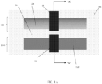
- FIG. 1A shows a top view of a structure
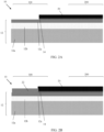
- FIG. 1B shows a cross-sectional view of the structure of FIG. 1A along line "A"-"A” in accordance with aspects of the present disclosure.
- the structure 10 shown in FIGS. 1A and 1B includes a substrate 12.
- the substrate 12 may be fully depleted semiconductor-on-insulator (FSDOI) technology comprising a handle substrate 12a, a buried insulator layer (i.e., substrate) 12b and top semiconductor layers 12c, 12d isolated from each other by a shallow trench isolation structure 16.
- Shallow trench isolation structures 16a may be used to surround a PFET region 100 and NFET region 200.
- reference numeral 200 may also represent a non-graded cSiGe PFET.
- the handle substrate 12a may include a semiconductor material such as, for example, Si, Ge, SiGe, SiC, SiGeC, a III-V compound semiconductor, an II-VI compound semiconductor or any combinations thereof.
- the handle substrate 12a may preferably be a single crystalline p-type semiconductor substrate.
- the handle substrate 12a provides mechanical support to the buried insulator layer 12b and the top semiconductor layers 12c, 12d.
- the buried insulator layer 12b may include a dielectric material such as silicon dioxide, silicon nitride, silicon oxynitride, boron nitride or a combination thereof.
- the buried insulator layer 12b may be a buried oxide material, e.g., BOX, formed by a deposition process, such as chemical vapor deposition (CVD), plasma enhanced CVD (PECVD) or physical vapor deposition (PVD).
- CVD chemical vapor deposition
- PECVD plasma enhanced CVD
- PVD physical vapor deposition
- the buried insulator layer 12b may be formed using a thermal growth process or oxygen implantation processes as is known in the art.
- the top semiconductor layers 12c, 12d may be fully depleted semiconductor-on-insulator materials.
- the top semiconductor layer 12c may comprise a silicon channel (cSi); whereas the top semiconductor layer 12d may comprise cSiGe with a laterally graded Ge%.
- the top semiconductor layer 12c may be a channel region for an NFET region 200 and the top semiconductor layer 12d may be a channel region for a PFET region 100.
- the Ge% may be tuned along the width of the channel region of the PFET region 100, with a lower Ge% closest to the shallow trench isolation structure 16 at a boundary between the NFET region 200 and the PFET region 100 and a higher Ge% farther away from such boundary. It should be understood by those of ordinary skill in the art that the Ge% may be tuned laterally (e.g., horizontally along the width of the channel region) in the top semiconductor layer 12d with different Ge% in order to tune/increase Vt of the PFET region 100.
- Vt targeting is achievable by a net reduction in Ge%, with Ioff vs. Vtsat improvement due to a lower net Ge%.
- increased Ioff vs. Ieff performance can be achieved with adjustment of the Ge%, i.e., rather than relying on channel or well implant to achieve Vt targeting.
- an insulator layer 14, 14' may be provided over the channel regions, e.g., top semiconductor layer 12c and top semiconductor layer 12d.
- the insulator layer 14, 14' may be an oxide or high-k dielectric material.
- a notch or protuberance 14a extends within the top semiconductor layer 12d, e.g., a notch 14a at an upper surface of the top semiconductor layer 12d.
- the notch or protuberance 14a conformally contains the gate dielectric and gate material 18.
- the gate material 18 may be a gate metal or a polysilicon material.
- the notch or protuberance 14a may be provided at a transition point of the Ge% within the top semiconductor layer 12d, where a lower Ge% is provided on a side closest to the shallow trench isolation structure 16 at the boundary of the NFET region 200 and the PFET 100. More specifically, the notch or protuberance 14a may be present at a cSi/cSiGe boundary.
- the gate material 18 may be provided on the insulator layer 14, 14' over the channel regions, e.g., top semiconductor layers 12c, 12d of the PFET region 100 and NFET region 200.
- the gate material 18 may extend partially within the conformally formed notch 14a, and may be any known workfunction materials or combinations thereof used in the PFET region 100 and the NFET region 200.
- the workfunction materials may include any suitable metals such as, but not limited to, Ti, TiAlC, Al, TiAl, TaN, TaAlC, TiN, TiC, TaC and Co or combinations thereof.
- the workfunction materials may be formed by CVD, PVD including sputtering, atomic layer deposition (ALD) or other suitable method, followed by a patterning process as further described below.
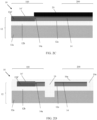
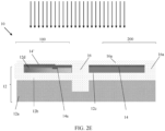
- FIGS. 2A-2E show fabrication processes of manufacturing the structure 10 of FIGS. 1A and 1B .
- an insulator layer 14 and masking layer 20 may be formed on the substate 12 and more particularly on the semiconductor-on-insulator material 12c.
- the semiconductor-on-insulator material 12c may be fully depleted cSi.
- the insulator layer 14 may be a pad oxide that is deposited by a conventional deposition process, e.g., CVD.
- the mask layer 20 may be a pad nitride material deposited by a conventional deposition process, e.g., CVD.
- the insulator layer 14 and mask layer 20 may be patterned to overlap onto a portion of the PFET region 100 of the structure 10. For example, through the use of conventional lithography and etching processes, the insulator layer 14 and mask layer 20 may be patterned with a portion of the insulator layer 14 and mask layer 20 remaining over the PFET region 100 of the structure 10.
- the overlap of the insulator layer 14 and mask layer 20 on the PFET side of the 100 may be tuned to assist in the formation of the laterally graded cSiGe channel of the PFET 100. For example, as described herein, by adjusting the extent of the overlap of the insulator layer 14 and mask layer 20, it is possible to tune the Ge% in the channel of the PFET region 100.
- a cSiGe material 22 may be provided over the exposed portion of the semiconductor-on-insulator material 12c on the PFET region 100 of the structure 10.
- the cSiGe material 22 may be epitaxially grown on the semiconductor-on-insulator material 12c, with the insulator layer 14 and mask layer 20 preventing growth of this material over the NFET region 200 of the structure 10.
- the structure 10 undergoes a thermal condensation process to drive the cSiGe material 22 into the semiconductor-on-insulator material 12c on the PFET region 100 of the structure 10.
- the thermal condensation process is a thermal oxidation process which results in Ge material being transported from the epitaxial cSiGe to the device layer, e.g., channel region of the PFET region 100, forming cSiGe layer 12d'.
- the thermal oxidation process will also result in the cSiGe material converting to insulator (e.g., oxide) material 14' over the channel region, e.g., cSiGe layer 12d'.
- This process will also result in the formation of the notch or protuberance 14a at a transition between cSiGe material 12d' and the semiconductor-on-insulator material 12c, e.g., cSi.
- the mask layer 20 may be removed and shallow trench isolation structures 16, 16a may be formed in the structure 10.
- the shallow trench isolation structure 16 is provided at a boundary between the PFET region 100 and the NFET region 200.
- the shallow trench isolation structure 16 may be provided at a side of the notch or protuberance 14a, and may also be deeper than the shallow trench isolation structures 16a. Compared to conventional fabrication processes, the notch or protuberance 14a is preserved in the PFET region 100.
- the shallow trench isolation structures 16, 16a can be formed by conventional lithography, etching and deposition methods known to those of skill in the art. For example, a resist formed over the insulator material 14, 14' is exposed to energy (light) and developed utilizing a conventional resist developer to form a pattern (openings). An etching process with a selective chemistry, e.g., reactive ion etching (RIE), will be used to transfer the pattern from the photoresist layer to the substrate 12 to form trenches.
- RIE reactive ion etching
- the insulator material can be deposited by any conventional deposition processes, e.g., CVD processes to form the shallow trench isolation structures 16, 16a.
- the insulator material of the shallow trench isolation structures 16a may be planarized by a conventional CMP process. Additional insulator material can also be deposited by CVD on the surface of the insulator material 14, 14'.
- the structure undergoes an anneal process to blend or drive the cSiGe material 12d' into the channel region 12d of the PFET 100.
- the annealing process may be about 750° C and, more preferably about 800° C to 900° C, and more preferably between 900° C to 1100° C to provide or adjust a diffusion of Ge into the channel region.
- the channel region of the NFET region 200 i.e., Si channel
- this layer will remain a non-graded fully depleted semiconductor-on-insulator channel region.
- the Ge% may be tuned along the width of the channel region (e.g., top semiconductor layer 12d) by adjusting the overlap of the insulator layer 14 and mask layer 20 and, more specifically, the mask layer 20. For example, adjusting the overlap to be greater over the PFET region 100, will result in less exposed semiconductor material on the PFET region 100. This, in turn, will result in less cSiGe material 22 epitaxially grown over the channel region of the PFET region 100 and, hence, a reduced concentration of Ge in the top semiconductor layer 12d. Following the anneal process, a lower Ge% will be provided at the boundary between the PFET region 100 and NFET region 200.
- adjusting the overlap to be less over the PFET region 100 will result in more cSiGe material 22 (of FIG. 2B ) epitaxially grown over the channel region of the PFET region 100 and, hence, increased a concentration of Ge in the top semiconductor layer 12d. This will result in a higher Ge% at the boundary between the PFET region 100 and NFET 200.
- the Ge will diffuse into the cSi material and provide a lateral gradient of Ge% with a Ge% greatest at one end and lowest at an opposite end (e.g., nearest to the boundary of the PFET region 100 and the NFET region 200). Accordingly, the PFET region 100 can be tuned with different Ge% in the channel region of the PFET region 100.
- the gate structures (gate material 18) for the PFET region 100 and NFET region 200 may be fabricated using conventional CMOS processes.
- a workfunction metal 18 may be deposited on the insulator material 14 by a conventional CVD process, followed by a conventional patterning process.
- the same or different gate materials 18, e.g., workfunction materials can be used for the PFET region 100 and the NFET 200.
- the workfunction material(s) 18 for both the PFET region 100 and the NFET region 200 can be deposited and patterned at the same time.
- the PFET region 100 and the NFET region 200 can be deposited and patterned in different fabrication processes.
- Sidewall spacers may be formed on the sidewalls of the gate material(s) 18.
- the sidewall spacers may be a nitride material or combination of nitride and oxide, blanket deposited over the gate material(s) followed by an anisotropic etching process to form sidewall spacers as is known in the art such that no further explanation is required for a complete understanding of the present disclosure.
- SoC system on chip
- the SoC is an integrated circuit (also known as a "chip") that integrates all components of an electronic system on a single chip or substrate. As the components are integrated on a single substrate, SoCs consume much less power and take up much less area than multichip designs with equivalent functionality. Because of this, SoCs are becoming the dominant force in the mobile computing (such as in Smartphones) and edge computing markets. SoC is also used in embedded systems and the Internet of Things.
- the method(s) as described above is used in the fabrication of integrated circuit chips.
- the resulting integrated circuit chips can be distributed by the fabricator in raw wafer form (that is, as a single wafer that has multiple unpackaged chips), as a bare die, or in a packaged form.
- the chip is mounted in a single chip package (such as a plastic carrier, with leads that are affixed to a motherboard or other higher level carrier) or in a multichip package (such as a ceramic carrier that has either or both surface interconnections or buried interconnections).
- the chip is then integrated with other chips, discrete circuit elements, and/or other signal processing devices as part of either (a) an intermediate product, such as a motherboard, or (b) an end product.
- the end product can be any product that includes integrated circuit chips, ranging from toys and other low-end applications to advanced computer products having a display, a keyboard or other input device, and a central processor.
Landscapes
- Metal-Oxide And Bipolar Metal-Oxide Semiconductor Integrated Circuits (AREA)
Abstract
Description
- The present disclosure relates to semiconductor structures and, more particularly, to a device with a laterally graded channel region and methods of manufacture.
- A silicon-on-insulator substrate permits device operation at significantly higher speeds with improved electrical isolation and reduced electrical losses in comparison with field-effect transistors built using a bulk silicon wafer. Generally, a silicon-on-insulator substrate includes a thin device layer of semiconductor material, a substrate, and a buried oxide layer physically separating and electrically isolating the device layer from the substrate. Contingent on the thickness of the device layer, a field-effect transistor may operate in a fully depleted mode in which a depletion layer in the channel region extends fully to the buried oxide layer when typical control voltages are applied to the gate electrode.
- The channel region of a fully depleted p-type field-effect transistor may be composed of silicon-germanium. A conventional approach for forming the silicon-germanium channel region is to grow an epitaxial silicon-germanium layer on a section of the device layer and to perform a thermal condensation process. Germanium is transported from the epitaxial silicon-germanium layer to the device layer and throughout the channel region down to the buried oxide layer. The silicon-germanium channel region formed by the thermal condensation process may be prone to strain relaxation and broken bonds at an interface with the buried oxide layer. The broken bonds may elevate the interface trap density at the interface, and the strain relaxation may impact device performance through a loss of carrier mobility. To improve this issue, in known solutions, the silicon-germanium channel region may have a vertical gradient of a percentage concentration of germanium (Ge%).
- In an aspect of the disclosure, a structure comprises a PFET region comprising a laterally graded semiconductor channel region under a gate material.
- Additional features of the structure are set forth in dependent claims 2 to 9.
- In an aspect of the disclosure, a structure comprises: a PFET device with a channel region comprising a laterally graded semiconductor-on-insulator material; another device with a channel region comprising a non-laterally graded semiconductor-on insulator-material; and a trench isolation structure isolating the PFET device from the other device.
- Additional features of the structure are set forth in dependent claims 11 to 14.
- In an aspect of the disclosure, a method comprises: forming a PFET device with a channel region comprising a laterally graded semiconductor-on-insulator material; forming an NFET device with a channel region comprising a non-laterally graded semiconductor-on-insulator material; and forming a trench isolation structure isolating the PFET device from the NFET device.
- The present disclosure is described in the detailed description which follows, in reference to the noted plurality of drawings by way of non-limiting examples of exemplary embodiments of the present disclosure.
-
FIG. 1A shows a top view of a structure with a graded channel region in accordance with aspects of the present disclosure. -
FIG. 1B shows a cross-sectional view of the structure ofFIG. 1A along line "A"-"A". -
FIGS. 2A-2E show fabrication processes of manufacturing the structure shown inFIGS. 1A and1B . - The present disclosure relates to semiconductor structures and, more particularly, to a device with a laterally graded channel region and methods of manufacture. More specifically, the structure includes a device with a laterally graded Silicon-Germanium channel (cSiGe) layer. In embodiments, the device may be a high voltage threshold (HVT) PFET using fully depleted semiconductor-on-insulator technology. Advantageously, the use of the laterally graded cSiGe layer significantly improves device performance compared to conventional devices, e.g., improves Ion vs. Ioff performance. In addition, fabrication processes eliminate a masking step required in conventional fabrication processes, while also allowing Vtsat to be independently tuned.
- In more specific embodiments, the device may be a high threshold voltage PFET. In embodiments, the PFET may include a reduced Ge% at the boundary of the channel region. In further embodiments, the Ge% may be graded horizontal in the channel region of the PFET device such that a lower Ge% is proximate an NFET region. The Ge% may be tuned for different device performances by lithography processes as described herein. For example, with the processes described herein, it is now possible to provide selective inclusion of cSiGe in the active channel region to form a lateral Ge% grading.
- The structure of the present disclosure can be manufactured in a number of ways using a number of different tools. In general, though, the methodologies and tools are used to form structures with dimensions in the micrometer and nanometer scale. The methodologies, i.e., technologies, employed to manufacture the structure of the present disclosure have been adopted from integrated circuit (IC) technology. For example, the structures are built on wafers and are realized in films of material patterned by photolithographic processes on the top of a wafer. In particular, the fabrication of the structure uses three basic building blocks: (i) deposition of thin films of material on a substrate, (ii) applying a patterned mask on top of the films by photolithographic imaging, and (iii) etching the films selectively to the mask. In addition, precleaning processes may be used to clean etched surfaces of any contaminants, as is known in the art. Moreover, when necessary, rapid thermal anneal processes may be used to drive-in dopants or material layers as is known in the art.
-
FIG. 1A shows a top view of a structure andFIG. 1B shows a cross-sectional view of the structure ofFIG. 1A along line "A"-"A" in accordance with aspects of the present disclosure. More specifically, thestructure 10 shown inFIGS. 1A and1B includes asubstrate 12. In embodiments, thesubstrate 12 may be fully depleted semiconductor-on-insulator (FSDOI) technology comprising ahandle substrate 12a, a buried insulator layer (i.e., substrate) 12b andtop semiconductor layers trench isolation structure 16. Shallowtrench isolation structures 16a may be used to surround aPFET region 100 and NFETregion 200. In embodiments,reference numeral 200 may also represent a non-graded cSiGe PFET. - The
handle substrate 12a may include a semiconductor material such as, for example, Si, Ge, SiGe, SiC, SiGeC, a III-V compound semiconductor, an II-VI compound semiconductor or any combinations thereof. Thehandle substrate 12a may preferably be a single crystalline p-type semiconductor substrate. Thehandle substrate 12a provides mechanical support to the buriedinsulator layer 12b and thetop semiconductor layers - The buried
insulator layer 12b may include a dielectric material such as silicon dioxide, silicon nitride, silicon oxynitride, boron nitride or a combination thereof. In preferred embodiments, the buriedinsulator layer 12b may be a buried oxide material, e.g., BOX, formed by a deposition process, such as chemical vapor deposition (CVD), plasma enhanced CVD (PECVD) or physical vapor deposition (PVD). In alternative embodiments, the buriedinsulator layer 12b may be formed using a thermal growth process or oxygen implantation processes as is known in the art. - The
top semiconductor layers top semiconductor layer 12c may comprise a silicon channel (cSi); whereas thetop semiconductor layer 12d may comprise cSiGe with a laterally graded Ge%. Thetop semiconductor layer 12c may be a channel region for an NFETregion 200 and thetop semiconductor layer 12d may be a channel region for aPFET region 100. - In embodiments, the Ge% may be tuned along the width of the channel region of the
PFET region 100, with a lower Ge% closest to the shallowtrench isolation structure 16 at a boundary between theNFET region 200 and thePFET region 100 and a higher Ge% farther away from such boundary. It should be understood by those of ordinary skill in the art that the Ge% may be tuned laterally (e.g., horizontally along the width of the channel region) in thetop semiconductor layer 12d with different Ge% in order to tune/increase Vt of thePFET region 100. For example, Vt targeting is achievable by a net reduction in Ge%, with Ioff vs. Vtsat improvement due to a lower net Ge%. Also, increased Ioff vs. Ieff performance can be achieved with adjustment of the Ge%, i.e., rather than relying on channel or well implant to achieve Vt targeting. - Still referring to
FIGS. 1A and1B , aninsulator layer 14, 14' may be provided over the channel regions, e.g.,top semiconductor layer 12c andtop semiconductor layer 12d. In embodiments, theinsulator layer 14, 14' may be an oxide or high-k dielectric material. A notch orprotuberance 14a extends within thetop semiconductor layer 12d, e.g., anotch 14a at an upper surface of thetop semiconductor layer 12d. In embodiments, the notch orprotuberance 14a conformally contains the gate dielectric andgate material 18. Thegate material 18 may be a gate metal or a polysilicon material. The notch orprotuberance 14a may be provided at a transition point of the Ge% within thetop semiconductor layer 12d, where a lower Ge% is provided on a side closest to the shallowtrench isolation structure 16 at the boundary of theNFET region 200 and thePFET 100. More specifically, the notch orprotuberance 14a may be present at a cSi/cSiGe boundary. - The
gate material 18 may be provided on theinsulator layer 14, 14' over the channel regions, e.g.,top semiconductor layers PFET region 100 andNFET region 200. Thegate material 18 may extend partially within the conformally formednotch 14a, and may be any known workfunction materials or combinations thereof used in thePFET region 100 and theNFET region 200. For example, the workfunction materials may include any suitable metals such as, but not limited to, Ti, TiAlC, Al, TiAl, TaN, TaAlC, TiN, TiC, TaC and Co or combinations thereof. The workfunction materials may be formed by CVD, PVD including sputtering, atomic layer deposition (ALD) or other suitable method, followed by a patterning process as further described below. -
FIGS. 2A-2E show fabrication processes of manufacturing thestructure 10 ofFIGS. 1A and1B . InFIG. 2A , aninsulator layer 14 andmasking layer 20 may be formed on thesubstate 12 and more particularly on the semiconductor-on-insulator material 12c. In embodiments, at this fabrication stage, the semiconductor-on-insulator material 12c may be fully depleted cSi. Theinsulator layer 14 may be a pad oxide that is deposited by a conventional deposition process, e.g., CVD. Themask layer 20 may be a pad nitride material deposited by a conventional deposition process, e.g., CVD. - The
insulator layer 14 andmask layer 20 may be patterned to overlap onto a portion of thePFET region 100 of thestructure 10. For example, through the use of conventional lithography and etching processes, theinsulator layer 14 andmask layer 20 may be patterned with a portion of theinsulator layer 14 andmask layer 20 remaining over thePFET region 100 of thestructure 10. The overlap of theinsulator layer 14 andmask layer 20 on the PFET side of the 100 may be tuned to assist in the formation of the laterally graded cSiGe channel of thePFET 100. For example, as described herein, by adjusting the extent of the overlap of theinsulator layer 14 andmask layer 20, it is possible to tune the Ge% in the channel of thePFET region 100. - In
FIG. 2B , acSiGe material 22 may be provided over the exposed portion of the semiconductor-on-insulator material 12c on thePFET region 100 of thestructure 10. ThecSiGe material 22 may be epitaxially grown on the semiconductor-on-insulator material 12c, with theinsulator layer 14 andmask layer 20 preventing growth of this material over theNFET region 200 of thestructure 10. - In
FIG. 2C , thestructure 10 undergoes a thermal condensation process to drive thecSiGe material 22 into the semiconductor-on-insulator material 12c on thePFET region 100 of thestructure 10. In embodiments, the thermal condensation process is a thermal oxidation process which results in Ge material being transported from the epitaxial cSiGe to the device layer, e.g., channel region of thePFET region 100, formingcSiGe layer 12d'. The thermal oxidation process will also result in the cSiGe material converting to insulator (e.g., oxide) material 14' over the channel region, e.g.,cSiGe layer 12d'. This process will also result in the formation of the notch orprotuberance 14a at a transition betweencSiGe material 12d' and the semiconductor-on-insulator material 12c, e.g., cSi. - As further shown in
FIG. 2D , themask layer 20 may be removed and shallowtrench isolation structures structure 10. As should be understood, the shallowtrench isolation structure 16 is provided at a boundary between thePFET region 100 and theNFET region 200. In embodiments, the shallowtrench isolation structure 16 may be provided at a side of the notch orprotuberance 14a, and may also be deeper than the shallowtrench isolation structures 16a. Compared to conventional fabrication processes, the notch orprotuberance 14a is preserved in thePFET region 100. - In embodiments, the shallow
trench isolation structures insulator material 14, 14' is exposed to energy (light) and developed utilizing a conventional resist developer to form a pattern (openings). An etching process with a selective chemistry, e.g., reactive ion etching (RIE), will be used to transfer the pattern from the photoresist layer to thesubstrate 12 to form trenches. Following the resist removal by a conventional oxygen ashing process or other known stripants, the insulator material can be deposited by any conventional deposition processes, e.g., CVD processes to form the shallowtrench isolation structures trench isolation structures 16a may be planarized by a conventional CMP process. Additional insulator material can also be deposited by CVD on the surface of theinsulator material 14, 14'. - As shown in
FIG. 2E , the structure undergoes an anneal process to blend or drive thecSiGe material 12d' into thechannel region 12d of thePFET 100. In this way, it is possible to provide a laterally graded Ge% into thechannel region 12d of thePFET region 100. In embodiments, the annealing process may be about 750° C and, more preferably about 800° C to 900° C, and more preferably between 900° C to 1100° C to provide or adjust a diffusion of Ge into the channel region. As the channel region of theNFET region 200, i.e., Si channel, remains protected from the cSiGe, this layer will remain a non-graded fully depleted semiconductor-on-insulator channel region. - In embodiments, the Ge% may be tuned along the width of the channel region (e.g.,
top semiconductor layer 12d) by adjusting the overlap of theinsulator layer 14 andmask layer 20 and, more specifically, themask layer 20. For example, adjusting the overlap to be greater over thePFET region 100, will result in less exposed semiconductor material on thePFET region 100. This, in turn, will result inless cSiGe material 22 epitaxially grown over the channel region of thePFET region 100 and, hence, a reduced concentration of Ge in thetop semiconductor layer 12d. Following the anneal process, a lower Ge% will be provided at the boundary between thePFET region 100 andNFET region 200. - On the other hand, adjusting the overlap to be less over the
PFET region 100 will result in more cSiGe material 22 (ofFIG. 2B ) epitaxially grown over the channel region of thePFET region 100 and, hence, increased a concentration of Ge in thetop semiconductor layer 12d. This will result in a higher Ge% at the boundary between thePFET region 100 andNFET 200. In either scenario, due to the annealing process the Ge will diffuse into the cSi material and provide a lateral gradient of Ge% with a Ge% greatest at one end and lowest at an opposite end (e.g., nearest to the boundary of thePFET region 100 and the NFET region 200). Accordingly, thePFET region 100 can be tuned with different Ge% in the channel region of thePFET region 100. - Referring back to
FIGS. 1A and1B , the gate structures (gate material 18) for thePFET region 100 andNFET region 200 may be fabricated using conventional CMOS processes. For example, in conventional CMOS processing, aworkfunction metal 18 may be deposited on theinsulator material 14 by a conventional CVD process, followed by a conventional patterning process. In embodiments, the same ordifferent gate materials 18, e.g., workfunction materials, can be used for thePFET region 100 and theNFET 200. In the case of using the same materials, the workfunction material(s) 18 for both thePFET region 100 and theNFET region 200 can be deposited and patterned at the same time. In the case of using different materials, thePFET region 100 and theNFET region 200 can be deposited and patterned in different fabrication processes. - Sidewall spacers may be formed on the sidewalls of the gate material(s) 18. In embodiments, the sidewall spacers may be a nitride material or combination of nitride and oxide, blanket deposited over the gate material(s) followed by an anisotropic etching process to form sidewall spacers as is known in the art such that no further explanation is required for a complete understanding of the present disclosure.
- The structure can be utilized in system on chip (SoC) technology. The SoC is an integrated circuit (also known as a "chip") that integrates all components of an electronic system on a single chip or substrate. As the components are integrated on a single substrate, SoCs consume much less power and take up much less area than multichip designs with equivalent functionality. Because of this, SoCs are becoming the dominant force in the mobile computing (such as in Smartphones) and edge computing markets. SoC is also used in embedded systems and the Internet of Things.
- The method(s) as described above is used in the fabrication of integrated circuit chips. The resulting integrated circuit chips can be distributed by the fabricator in raw wafer form (that is, as a single wafer that has multiple unpackaged chips), as a bare die, or in a packaged form. In the latter case the chip is mounted in a single chip package (such as a plastic carrier, with leads that are affixed to a motherboard or other higher level carrier) or in a multichip package (such as a ceramic carrier that has either or both surface interconnections or buried interconnections). In any case the chip is then integrated with other chips, discrete circuit elements, and/or other signal processing devices as part of either (a) an intermediate product, such as a motherboard, or (b) an end product. The end product can be any product that includes integrated circuit chips, ranging from toys and other low-end applications to advanced computer products having a display, a keyboard or other input device, and a central processor.
- The descriptions of the various embodiments of the present disclosure have been presented for purposes of illustration, but are not intended to be exhaustive or limited to the embodiments disclosed. Many modifications and variations will be apparent to those of ordinary skill in the art without departing from the scope and spirit of the described embodiments. The terminology used herein was chosen to best explain the principles of the embodiments, the practical application or technical improvement over technologies found in the marketplace, or to enable others of ordinary skill in the art to understand the embodiments disclosed herein.
Claims (15)
- A structure comprising a PFET region comprising a laterally graded semiconductor channel region under a gate material.
- The structure of claim 1, wherein the laterally graded semiconductor channel region comprises cSiGe.
- The structure of claim 2, wherein the laterally graded semiconductor channel region comprises a laterally graded Ge% along a horizontal extent of the laterally graded semiconductor channel region.
- The structure of claim 3, further comprising a notch extended within the laterally graded semiconductor channel region, wherein, optionally, the notch is at a transition between the cSiGe and cSi.
- The structure of claim 4, further comprising a non-graded NFET region adjacent to the PFET region.
- The structure of claim 2, further comprising an NFET region comprising a channel region of a non-graded fully depleted semiconductor-on-insulator material, wherein, optionally, the non-graded fully depleted semiconductor-on-insulator material comprises cSi.
- The structure of claim 6, further comprising a shallow trench isolation structure isolating the PFET region from the NFET region.
- The structure of claim 6 or 7, wherein a Ge% of the laterally graded semiconductor channel region comprising cSiGe is lower as it reaches a boundary between the PFET region and the NFET region.
- The structure of one of claims 1 to 8, wherein the laterally graded semiconductor channel region comprises cSiGe with a Ge% greatest at one end and lowest at an opposite end, and a notch at an upper surface.
- A structure comprising:a PFET device with a channel region comprising a laterally graded semiconductor-on-insulator material;another device with a channel region comprising a non-laterally graded semiconductor-on-insulator material; anda trench isolation structure isolating the PFET device from the other device.
- The structure of claim 10, wherein the laterally graded semiconductor-on-insulator material comprises cSiGe with an increasing Ge% along a length, and/or wherein e non-laterally graded semiconductor-on-insulator material comprises cSi.
- The structure of claim 11, wherein the cSiGe transitions to cSi.
- The structure of claim 12, further comprising a notch comprising insulator material extending into the cSiGe, wherein the notch is at a location where the cSiGe transitions to the cSi.
- The structure of one of claims 11 to 13, wherein the Ge% is lowest at a boundary between the PFET device and the NFET device, and/or wherein the Ge% is greatest at one end and lowest at an opposite end nearest the NFET device.
- A method comprising:forming a PFET device with a channel region comprising a laterally graded semiconductor-on-insulator material;forming an NFET device with a channel region comprising a non-laterally graded semiconductor-on-insulator material; andforming a trench isolation structure isolating the PFET device from the NFET device.
Applications Claiming Priority (1)
| Application Number | Priority Date | Filing Date | Title |
|---|---|---|---|
| US17/968,404 US20240128322A1 (en) | 2022-10-18 | 2022-10-18 | Device with laterally graded channel region |
Publications (1)
| Publication Number | Publication Date |
|---|---|
| EP4358124A1 true EP4358124A1 (en) | 2024-04-24 |
Family
ID=87971961
Family Applications (1)
| Application Number | Title | Priority Date | Filing Date |
|---|---|---|---|
| EP23195573.3A Pending EP4358124A1 (en) | 2022-10-18 | 2023-09-06 | Device with laterally graded channel region |
Country Status (3)
| Country | Link |
|---|---|
| US (1) | US20240128322A1 (en) |
| EP (1) | EP4358124A1 (en) |
| CN (1) | CN117913094A (en) |
Citations (2)
| Publication number | Priority date | Publication date | Assignee | Title |
|---|---|---|---|---|
| US3374406A (en) * | 1964-06-01 | 1968-03-19 | Rca Corp | Insulated-gate field-effect transistor |
| US20170256565A1 (en) * | 2016-03-03 | 2017-09-07 | Globalfoundries Inc. | Field-effect transistors with a non-relaxed strained channel |
Family Cites Families (1)
| Publication number | Priority date | Publication date | Assignee | Title |
|---|---|---|---|---|
| EP1397832A2 (en) * | 2001-06-08 | 2004-03-17 | Amberwave Systems Corporation | Method for isolating semiconductor devices |
-
2022
- 2022-10-18 US US17/968,404 patent/US20240128322A1/en active Pending
-
2023
- 2023-09-06 EP EP23195573.3A patent/EP4358124A1/en active Pending
- 2023-09-18 CN CN202311200860.5A patent/CN117913094A/en active Pending
Patent Citations (2)
| Publication number | Priority date | Publication date | Assignee | Title |
|---|---|---|---|---|
| US3374406A (en) * | 1964-06-01 | 1968-03-19 | Rca Corp | Insulated-gate field-effect transistor |
| US20170256565A1 (en) * | 2016-03-03 | 2017-09-07 | Globalfoundries Inc. | Field-effect transistors with a non-relaxed strained channel |
Also Published As
| Publication number | Publication date |
|---|---|
| US20240128322A1 (en) | 2024-04-18 |
| CN117913094A (en) | 2024-04-19 |
Similar Documents
| Publication | Publication Date | Title |
|---|---|---|
| US9647118B2 (en) | Device having EPI film in substrate trench | |
| US8012820B2 (en) | Ultra-thin SOI CMOS with raised epitaxial source and drain and embedded SiGe PFET extension | |
| US7393732B2 (en) | Double silicon-on-insulator (SOI) metal oxide semiconductor field effect transistor (MOSFET) structures | |
| US8298895B1 (en) | Selective threshold voltage implants for long channel devices | |
| US20120313168A1 (en) | Formation of embedded stressor through ion implantation | |
| US11798948B2 (en) | Semiconductor structure with shared well | |
| US7648880B2 (en) | Nitride-encapsulated FET (NNCFET) | |
| EP4401123A1 (en) | Device with isolation structures in active regions | |
| US11843034B2 (en) | Lateral bipolar transistor | |
| US10680065B2 (en) | Field-effect transistors with a grown silicon-germanium channel | |
| US12289913B1 (en) | Device with metal field plate extension | |
| US7541629B1 (en) | Embedded insulating band for controlling short-channel effect and leakage reduction for DSB process | |
| US20250056831A1 (en) | Asymmetric junctionless fin field effect transistors | |
| US20240128322A1 (en) | Device with laterally graded channel region | |
| US10468310B2 (en) | Spacer integration scheme for FNET and PFET devices | |
| US20240395932A1 (en) | Wraparound gate structure | |
| US20250234585A1 (en) | Extended drain metal oxide semiconductor (edmos) field effect transistor (fet) with dual thickness semiconductor material | |
| US20260143778A1 (en) | Body contacted transistors | |
| US12495575B2 (en) | Multi-channel replacement metal gate device | |
| US20250015181A1 (en) | Metal-oxide semiconductor transistors | |
| US12349444B1 (en) | Under-source body contact | |
| US11605649B2 (en) | Switches in bulk substrate | |
| US20260123005A1 (en) | Transistor with field plate | |
| US20250040167A1 (en) | Gate-all-around field effect transistors | |
| US20260068279A1 (en) | Extended drain metal oxide semiconductor device |
Legal Events
| Date | Code | Title | Description |
|---|---|---|---|
| PUAI | Public reference made under article 153(3) epc to a published international application that has entered the european phase |
Free format text: ORIGINAL CODE: 0009012 |
|
| STAA | Information on the status of an ep patent application or granted ep patent |
Free format text: STATUS: THE APPLICATION HAS BEEN PUBLISHED |
|
| AK | Designated contracting states |
Kind code of ref document: A1 Designated state(s): AL AT BE BG CH CY CZ DE DK EE ES FI FR GB GR HR HU IE IS IT LI LT LU LV MC ME MK MT NL NO PL PT RO RS SE SI SK SM TR |
|
| STAA | Information on the status of an ep patent application or granted ep patent |
Free format text: STATUS: REQUEST FOR EXAMINATION WAS MADE |
|
| 17P | Request for examination filed |
Effective date: 20240625 |
|
| RBV | Designated contracting states (corrected) |
Designated state(s): AL AT BE BG CH CY CZ DE DK EE ES FI FR GB GR HR HU IE IS IT LI LT LU LV MC ME MK MT NL NO PL PT RO RS SE SI SK SM TR |