EP4358086A1 - Single ended sense amplifier with current pulse circuit - Google Patents
Single ended sense amplifier with current pulse circuit Download PDFInfo
- Publication number
- EP4358086A1 EP4358086A1 EP23192048.9A EP23192048A EP4358086A1 EP 4358086 A1 EP4358086 A1 EP 4358086A1 EP 23192048 A EP23192048 A EP 23192048A EP 4358086 A1 EP4358086 A1 EP 4358086A1
- Authority
- EP
- European Patent Office
- Prior art keywords
- bit cell
- pulse
- output
- sense amplifier
- current
- Prior art date
- Legal status (The legal status is an assumption and is not a legal conclusion. Google has not performed a legal analysis and makes no representation as to the accuracy of the status listed.)
- Granted
Links
Images

Classifications
-
- G—PHYSICS
- G11—INFORMATION STORAGE
- G11C—STATIC STORES
- G11C7/00—Arrangements for writing information into, or reading information out from, a digital store
- G11C7/06—Sense amplifiers; Associated circuits, e.g. timing or triggering circuits
- G11C7/067—Single-ended amplifiers
-
- G—PHYSICS
- G11—INFORMATION STORAGE
- G11C—STATIC STORES
- G11C11/00—Digital stores characterised by the use of particular electric or magnetic storage elements; Storage elements therefor
- G11C11/02—Digital stores characterised by the use of particular electric or magnetic storage elements; Storage elements therefor using magnetic elements
- G11C11/16—Digital stores characterised by the use of particular electric or magnetic storage elements; Storage elements therefor using magnetic elements using elements in which the storage effect is based on magnetic spin effect
- G11C11/165—Auxiliary circuits
- G11C11/1673—Reading or sensing circuits or methods
-
- G—PHYSICS
- G11—INFORMATION STORAGE
- G11C—STATIC STORES
- G11C13/00—Digital stores characterised by the use of storage elements not covered by groups G11C11/00, G11C23/00, or G11C25/00
- G11C13/0002—Digital stores characterised by the use of storage elements not covered by groups G11C11/00, G11C23/00, or G11C25/00 using resistive RAM [RRAM] elements
- G11C13/0021—Auxiliary circuits
- G11C13/004—Reading or sensing circuits or methods
-
- G—PHYSICS
- G11—INFORMATION STORAGE
- G11C—STATIC STORES
- G11C7/00—Arrangements for writing information into, or reading information out from, a digital store
- G11C7/06—Sense amplifiers; Associated circuits, e.g. timing or triggering circuits
- G11C7/065—Differential amplifiers of latching type
-
- G—PHYSICS
- G11—INFORMATION STORAGE
- G11C—STATIC STORES
- G11C7/00—Arrangements for writing information into, or reading information out from, a digital store
- G11C7/06—Sense amplifiers; Associated circuits, e.g. timing or triggering circuits
- G11C7/08—Control thereof
-
- G—PHYSICS
- G11—INFORMATION STORAGE
- G11C—STATIC STORES
- G11C7/00—Arrangements for writing information into, or reading information out from, a digital store
- G11C7/10—Input/output [I/O] data interface arrangements, e.g. I/O data control circuits, I/O data buffers
- G11C7/1078—Data input circuits, e.g. write amplifiers, data input buffers, data input registers, data input level conversion circuits
- G11C7/109—Control signal input circuits
-
- G—PHYSICS
- G11—INFORMATION STORAGE
- G11C—STATIC STORES
- G11C7/00—Arrangements for writing information into, or reading information out from, a digital store
- G11C7/12—Bit line control circuits, e.g. drivers, boosters, pull-up circuits, pull-down circuits, precharging circuits, equalising circuits, for bit lines
-
- G—PHYSICS
- G11—INFORMATION STORAGE
- G11C—STATIC STORES
- G11C7/00—Arrangements for writing information into, or reading information out from, a digital store
- G11C7/14—Dummy cell management; Sense reference voltage generators
-
- G—PHYSICS
- G11—INFORMATION STORAGE
- G11C—STATIC STORES
- G11C13/00—Digital stores characterised by the use of storage elements not covered by groups G11C11/00, G11C23/00, or G11C25/00
- G11C13/0002—Digital stores characterised by the use of storage elements not covered by groups G11C11/00, G11C23/00, or G11C25/00 using resistive RAM [RRAM] elements
- G11C13/0021—Auxiliary circuits
- G11C13/004—Reading or sensing circuits or methods
- G11C2013/0042—Read using differential sensing, e.g. bit line [BL] and bit line bar [BLB]
-
- G—PHYSICS
- G11—INFORMATION STORAGE
- G11C—STATIC STORES
- G11C13/00—Digital stores characterised by the use of storage elements not covered by groups G11C11/00, G11C23/00, or G11C25/00
- G11C13/0002—Digital stores characterised by the use of storage elements not covered by groups G11C11/00, G11C23/00, or G11C25/00 using resistive RAM [RRAM] elements
- G11C13/0021—Auxiliary circuits
- G11C13/004—Reading or sensing circuits or methods
- G11C2013/0045—Read using current through the cell
-
- G—PHYSICS
- G11—INFORMATION STORAGE
- G11C—STATIC STORES
- G11C13/00—Digital stores characterised by the use of storage elements not covered by groups G11C11/00, G11C23/00, or G11C25/00
- G11C13/0002—Digital stores characterised by the use of storage elements not covered by groups G11C11/00, G11C23/00, or G11C25/00 using resistive RAM [RRAM] elements
- G11C13/0021—Auxiliary circuits
- G11C13/004—Reading or sensing circuits or methods
- G11C2013/0054—Read is performed on a reference element, e.g. cell, and the reference sensed value is used to compare the sensed value of the selected cell
-
- G—PHYSICS
- G11—INFORMATION STORAGE
- G11C—STATIC STORES
- G11C2207/00—Indexing scheme relating to arrangements for writing information into, or reading information out from, a digital store
- G11C2207/06—Sense amplifier related aspects
- G11C2207/063—Current sense amplifiers
Definitions
- the present disclosure provides a circuit structure and related method to improve performance of a single ended sense amplifier.
- Typical memory device architectures include sense amplifiers for reading data stored in bit cells, e.g., by amplifying a voltage level in the bit cell and comparing it to a reference voltage to characterize the data as being a logic low (e.g., a "zero") or a logic high (e.g., a "one").
- resistive sense memory cells include variable resistors (referred to herein as "bit cells") that can be programmed during a write operation with either a high resistance or a low resistance.
- bit cells variable resistors
- a single ended sense amplifier hereinafter “sense amplifier” detects and amplifies the resistive state of the resistor and outputs a logic high or low.
- Embodiments of the disclosure provides a memory circuit, comprising: a bit cell; a p-type metal-oxide semiconductor (PMOS) transistor having a drain connected to a data path of the bit cell; and a NAND gate having an output coupled to a gate of the PMOS device, wherein a first input of the NAND gate is controlled by a state of the bit cell.
- a p-type metal-oxide semiconductor (PMOS) transistor having a drain connected to a data path of the bit cell
- a NAND gate having an output coupled to a gate of the PMOS device, wherein a first input of the NAND gate is controlled by a state of the bit cell.
- FIG. 1 Another aspect of the disclosure includes any of the preceding aspects, and wherein memory circuit is embodied in one of a resistive random-access memory (RRAM) or a magnetoresistive random-access memory (MRAM).
- RRAM resistive random-access memory
- MRAM magnetoresistive random-access memory
- Another aspect of the disclosure includes any of the preceding aspects, and wherein a second input of the NAND gate is controlled by a pulse signal.
- bit cell comprises a resistive sense memory cell.
- Another aspect of the disclosure includes any of the preceding aspects, and wherein a source of the PMOS transistor is connected to a current source, and wherein the current source increases an applied read current to the data path with an injected current pulse in response to detection of a low to high transition of a resistive state of the bit cell.
- the memory circuit includes a sensing circuit having a reference resistor.
- the sensing circuit detects a voltage drop across the bit cell in response to an applied read current during a read operation and generates a high or low logic output at an output node of the sensing circuit.
- the pulse signal comprises an equalization start pulse and the state of the bit cell comprises a previous output logic value from the output node.
- Another aspect of the disclosure includes any of the preceding aspects, and further includes an equalization start circuit that generates the equalization start pulse from an equalization start signal, wherein the equalization start pulse is approximately 3 nanoseconds in duration and the equalization start signal is approximately 10 nanoseconds in duration.
- the read operation includes: a pre-equalization phase during which the sense amplifier is in an off state; an equalization phase during which the current pulse is selectively injected to a bit cell line based on a previous output at the output node and the applied read current is provided to the bit cell and a reference resistor; and an execution phase during which a voltage drop across the bit cell is compared to a voltage drop across reference resistor to determine a present logic output at the output node.
- a sense amplifier including: a bit cell coupled to a sensing circuit via a data path; a p-type metal-oxide semiconductor (PMOS) transistor having a drain connected to the data path; and a NAND gate having an output coupled to a gate of the PMOS transistor, wherein a first input of the NAND gate is controlled by an output node of the sensing circuit.
- PMOS metal-oxide semiconductor
- Another aspect of the disclosure includes any of the preceding aspects, and wherein the sense amplifier is embodied in one of a resistive random-access memory (RRAM) or a Magnetoresistive random-access memory (MRAM).
- RRAM resistive random-access memory
- MRAM Magnetoresistive random-access memory
- Another aspect of the disclosure includes any of the preceding aspects, and wherein a second input of the NAND gate is controlled by a pulse signal.
- pulse signal comprises an equalization start pulse and a state of the bit cell comprises a previous output logic value from the output node.
- Another aspect of the disclosure includes any of the preceding aspects, and wherein the current pulse is applied when a low to high transition of the resistive state of the bit cell is detected.
- Another aspect of the disclosure includes any of the preceding aspects, and wherein the current pulse is generated with a pulse generation circuit that includes a PMOS transistor that controls a current source.
- the pulse generation circuit further includes a NAND gate having an output that controls the PMOS transistor.
- the NAND gate has a first input for receiving an equalization start pulse and a second input for receiving a previous output state from the output node.
- the pulse generation circuit further includes an equalization start circuit that generates the equalization start pulse from an equalization start signal.
- the equalization start pulse is approximately 3 nanoseconds in duration and the equalization start signal is approximately 10 nanoseconds in duration.
- such phrasing is intended to encompass the first listed option (A) only, or the selection of the second listed option (B) only, or the selection of the third listed option (C) only, or the selection of the first and the second listed options (A and B), or the selection of the first and third listed options (A and C) only, or the selection of the second and third listed options (B and C) only, or the selection of all three options (A and B and C).
- This may be extended, as readily apparent by one of ordinary skill in the art, for as many items listed.
- aspects of the present disclosure provide an enhanced single ended sense amplifier for a memory device, such as an RRAM or MRAM, that utilizes a resistive sense memory cell ("bit cell") structure.
- the enhanced sense amplifier improves performance, e.g., by allowing read operations to be performed in a single clock cycle.
- RRAM devices and the like utilize bit cells that can be configured to have different electrical resistances to store different logic states.
- the resistance of the bit cells is detected during a read operation using a single ended sense amplifier that applies a read current and senses a voltage level associated with a voltage drop across the cell.
- Existing approaches generally require the use of two clock cycles to complete the read operation, which is a result of the slower speeds needed to process low to high data transitions.
- charging, sensing and decoding voltage drops across high bit cell resistances can require more than a single clock cycle using existing techniques when a previous resistive state was low, e.g., 10 k ⁇ .
- the present disclosure includes an enhancement to a sense amplifier that provides a parallel current path for the bit cell, which is activated during the initial read (i.e., "equalization") phase to reduce the charging time of the bit cell resistor required during low to high data transitions.
- the additional circuit component utilizes a masking technique to differentiate between low to high and high to low transitions. This masking technique ensures that the additional current is not injected when the previous resistive state was high.
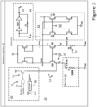
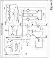
- Figures 1-3 depict an illustrative sense amplifier 12 that includes: (1) a bit cell 20; (2) a single ended sensing circuit 13; and (2) a pulse generation circuit 30.
- pulse generation circuit 30 provides a parallel current path that enhances performance by selectively injecting additional current to bit cell line 16 (i.e., data path of the bit cell) above switch S2.
- sense amplifier 12 is embedded in a memory device 10, such as an RRAM or MRAM, configured to store and retrieve data in bit cells 20.
- a typical memory device 10 includes many bit cells 20 and sense amplifiers 12, as well as other components such as controllers, logic, multiplexors, ECC decoders, etc., which are not shown but are readily understood by one skilled in the art.
- US Patent 7,852,665, Memory Cell with Proportional Current Self-Reference Sensing issued on December 14, 2010 , further describes such features, and is hereby incorporated by reference.
- sense amplifier 12 is configured to sense the resistive value of bit cell 20 and output logic values at output nodes OUT and OUTB. Resistance of the bit cell 20 is detected by applying a read current from Vdd across the bit cell 20 and reference resistor 14 (e.g., 50 k ⁇ ) to obtain a sensed data voltage drop (D1) and reference voltage drop (R1). The values at D1 and R1 are then compared to determine a logic value, e.g., if D1 is less than R1, the logic value is 0 and if D1 is greater than R1, the logic value is 1.
- sense amplifier 12 includes: a latch 40 that stores values for D1 / R1 and together with component 42 provides circuitry for comparing values D1 / R1; and an output component 44 for outputting a sensed logic value based on the comparison of D1 and R1.
- a pair of additional p-type metal-oxide semiconductor (PMOS) transistors Q15 and Q16, which limit the voltage/current across the bit cell during equalization phase are controlled by an input signal 62.
- PMOS p-type metal-oxide semiconductor
- a typical read operation of sense amplifier 12 can be described in three phases, referred to and shown herein as "pre-equalization” ( Figure 1 ), “equalization” ( Figure 2 ), and “execution” ( Figure 3 ).
- pre-equalization phase Figure 1
- switches S2, S3 and S4 are open, and switch S1 is closed.
- internal nodes D1 / R1 maintain the charge of the prior read operation and output component 44 maintains the logic state of prior read operation (0 or 1) in complementary OUT and OUTB nodes.
- All the switches are open except S1.
- Signal 60 which controls transistors Q9 and Q10, goes LOW turning off transistors Q9 and Q10.
- bit cell 20 and reference resistor 22 are not connected; therefore, there is no current path from Vdd to ground.
- switches S2 and S3 are closed completing the circuit between Vdd and ground via both the bit cell 20 and reference resistor 22, which causes the bit cell resistor R5 and reference resistor R6 22 to be charged.
- bit cell resistor R5 is currently at a high resistive state, e.g., 100k ⁇
- node D1 will be supplied with a voltage greater than the reference voltage (Vref) at node R1.
- bit cell resistor R5 is currently at a low resistive state, e.g., 10k ⁇
- node D1 will have a voltage less than the reference voltage (Vref) at node R1. Because switch S4 remains open during this phase, the output component 44 continues to maintain the logic state of a prior read operation in complementary OUT and OUTB nodes.
- switch S4 is closed and switch S1 is opened, causing compare components 40 and 42 to decode the value stored in bit cell 20.
- Components 40 and 42 compare currents created by a drop across the bit cell 20 and reference resistor 22.
- Component 42 is activated by signal 60, which is an execution signal that is high only in the execution phase (e.g., a 1 ns to 2.4 ns period) to activate transistors Q9 and Q10, to provide either a low or high logic value to output component 44.
- signal 60 is an execution signal that is high only in the execution phase (e.g., a 1 ns to 2.4 ns period) to activate transistors Q9 and Q10, to provide either a low or high logic value to output component 44.
- D1 is HIGH and R1 is LOW as shown
- a logic 1 is output at OUT and its complement 0 is output at OUTB.
- D1 is LOW and R1 is HIGH
- a logic 0 is provided to OUT and its complement 1 is
- bit cell 20 As noted, if the previous state of bit cell 20 was low (i.e., OUT was 0 and resistance of bit cell resistor R5 was low, e.g., 10kk ⁇ ), and the new state is high (i.e., resistance of R5 is 100kS2), the amount of time it takes to charge the bit cell 20 during the equalization phase ( Figure 2 ) is significantly higher than if the prior state was high because the current at bit cell resistor R5 is relatively low, e.g., only at about 2.6 ⁇ A. The additional time required to charge the bit cell 20 introduces a certain amount of latency into the read operation and, e.g., limits the ability to perform read operations in a single clock cycle.
- pulse generation circuit 30 provides a parallel current path to inject a current pulse during the equalization phase ( Figure 2 ) to raise the current at the bit cell line 16 above switch S2 when a transition from low to high occurs. This quickly charges line 16 and results in a shorter amount of time required to charge bit cell 20 and, e.g., allows the read operation to complete in a single clock cycle.
- pulse generation circuit 30 generally includes: (1) an equalization start circuit 36 that receives the equalization start signal (e.g., a 10 nanosecond signal) and outputs a shortened pulse signal of about 3 nanoseconds; (2) a NAND gate 32 that receives the pulse signal and the value at OUTB 14 (i.e., the logic state of the prior read operation); and (3) a p-type metal-oxide semiconductor (PMOS) transistor 34 that is gated, i.e., controlled, by the output of the NAND gate 32.
- the equalization start signal e.g., a 10 nanosecond signal
- a shortened pulse signal of about 3 nanoseconds
- a NAND gate 32 that receives the pulse signal and the value at OUTB 14 (i.e., the logic state of the prior read operation)
- PMOS p-type metal-oxide semiconductor
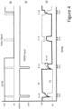
- Figure 4 depicts a timing diagram that shows the operation of pulse generation circuit 30.
- the top diagram 50 shows the inputs to NAND gate 32, i.e., OUTB and the pulse signal.
- the middle diagram 52 shows the PMOS transistor 34 input from the NAND gate 32 output.
- the transition time from a low to high (i.e., 0->1) transition at D1 (and opposite at R1) remains at about 12 nanoseconds (ns), the same as the other transitions.
- a typical threshold voltage difference between nodes D1 and R1 to indicate a high state may, for example, include any voltage greater than 80 mV.
- the method and structure as described above is used in the fabrication of integrated circuit chips.
- the resulting integrated circuit chips can be distributed by the fabricator in raw wafer form (that is, as a single wafer that has multiple unpackaged chips), as a bare die, or in a packaged form.
- the chip is mounted in a single chip package (such as a plastic carrier, with leads that are affixed to a motherboard or other higher-level carrier) or in a multichip package (such as a ceramic carrier that has either or both surface interconnections or buried interconnections).
- the chip is then integrated with other chips, discrete circuit elements, and/or other signal processing devices as part of either (a) an intermediate product, such as a motherboard, or (b) an end product.
- the end product can be any product that includes integrated circuit chips, ranging from toys and other low-end applications to advanced computer products having a display, a keyboard or other input device, and a center processor.
- Approximating language may be applied to modify any quantitative representation that could permissibly vary without resulting in a change in the basic function to which it is related. Accordingly, a value modified by a term or terms, such as “about,” “approximately,” and “substantially,” are not to be limited to the precise value specified. In at least some instances, the approximating language may correspond to the precision of an instrument for measuring the value.
- range limitations may be combined and/or interchanged, such ranges are identified and include all the sub-ranges contained therein unless context or language indicates otherwise. "Approximately” as applied to a particular value of a range applies to both values, and unless otherwise dependent on the precision of the instrument measuring the value, may indicate +/- 10% of the stated value(s).
- a memory circuit comprising: a bit cell; a p-type metal-oxide semiconductor (PMOS) transistor having a drain connected to a data path of the bit cell; and a NAND gate having an output coupled to a gate of the PMOS device, wherein a first input of the NAND gate is controlled by a state of the bit cell.
- PMOS metal-oxide semiconductor
- RRAM resistive random-access memory
- MRAM Magnetoresistive random-access memory
- bit cell comprises a resistive sense memory cell.
- a source of the PMOS transistor is connected to a current source, and wherein the current source increases an applied read current to the data path with an injected current pulse in response to detection of a low to high transition of a resistive state of the bit cell.
- sensing circuit detects a voltage drop across the bit cell in response to an applied read current during a read operation and generates a high or low logic output at an output node of the sensing circuit.
- pulse signal comprises an equalization start pulse and the state of the bit cell comprises a previous output logic value from the output node.
- a sense amplifier comprising: a bit cell coupled to a sensing circuit via a data path; a p-type metal-oxide semiconductor (PMOS) transistor having a drain connected to the data path; and a NAND gate having an output coupled to a gate of the PMOS transistor, wherein a first input of the NAND gate is controlled by an output node of the sensing circuit.
- PMOS metal-oxide semiconductor
- RRAM resistive random-access memory
- MRAM Magnetoresistive random-access memory
- pulse signal comprises an equalization start pulse and a state of the bit cell comprises a previous output logic value from the output node.
- a method for implementing a sense amplifier comprising: selectively injecting a current pulse to a bit cell line based on a previous logic value maintained at an output node, the bit cell line coupled to a bit cell that is configurable to a high or low resistance state; applying a read current to the bit cell and a reference resistor; and comparing a voltage drop across the bit cell (D1) to a voltage reference across the reference resistor (R1); and outputting a logic output at an output node based on a comparison of R1 and D1.
- the current pulse is generated with a pulse generation circuit that includes a p-type metal-oxide semiconductor (PMOS) transistor that controls a current source.
- PMOS p-type metal-oxide semiconductor
- the pulse generation circuit further includes a NAND gate having an output that controls the PMOS transistor.
- the pulse generation circuit further includes an equalization start circuit that generates the equalization start pulse from an equalization start signal.
- a sense amplifier comprising: a bit cell coupled to a data path for coupling to a sensing circuit via the data path; a p-type metal-oxide semiconductor (PMOS) transistor having a drain connected to the data path; and a NAND gate having an output coupled to a gate of the PMOS transistor, wherein a first input of the NAND gate is controlled by a state of the bit cell.
- the state may be detectable at an output node of the sensing circuit, e.g., the state may be given be represented by a previous output logic value from the output node. Accordingly, the NAND gate may be controlled by the output node of the sensing circuit.
- the sensing circuit may have a reference resistor.
- RRAM resistive random-access memory
- MRAM Magnetoresistive random-access memory
- a memory circuit comprising the sense amplifier of one of embodiments 21 to 25.
- RRAM resistive random-access memory
- MRAM Magnetoresistive random-access memory
- bit cell comprises a resistive sense memory cell.
- a source of the PMOS transistor is connected to a current source, and wherein the current source increases an applied read current to the data path with an injected current pulse in response to detection of a low to high transition of a resistive state of the bit cell.
- sensing circuit detects a voltage drop across the bit cell in response to an applied read current during a read operation and generates a high or low logic output at an output node of the sensing circuit.
- pulse signal comprises an equalization start pulse and the state of the bit cell comprises a previous output logic value from the output node.
- the memory circuit of embodiment 33 further comprising an equalization start circuit that generates the equalization start pulse from an equalization start signal, wherein the equalization start pulse is approximately 3 nanoseconds in duration and the equalization start signal is approximately 10 nanoseconds in duration.
- the memory circuit of one of embodiments 31 to 34 wherein the read operation includes: a pre-equalization phase during which the sensing circuit is in an off state; an equalization phase during which the current pulse is selectively injected to the data path of the bit cell based on a previous output at the output node and the applied read current is provided to the bit cell and a reference resistor; and an execution phase during which a voltage drop across the bit cell is compared to a voltage drop across the reference resistor to determine a present logic output at the output node.
Landscapes
- Engineering & Computer Science (AREA)
- Computer Hardware Design (AREA)
- Semiconductor Memories (AREA)
- Mram Or Spin Memory Techniques (AREA)
- Hall/Mr Elements (AREA)
Abstract
Description
- The present disclosure provides a circuit structure and related method to improve performance of a single ended sense amplifier.
- Typical memory device architectures include sense amplifiers for reading data stored in bit cells, e.g., by amplifying a voltage level in the bit cell and comparing it to a reference voltage to characterize the data as being a logic low (e.g., a "zero") or a logic high (e.g., a "one"). In certain memory device architectures, such as RRAM (resistive random-access memory) and MRAM (magnetoresistive randon-access memory), resistive sense memory cells include variable resistors (referred to herein as "bit cells") that can be programmed during a write operation with either a high resistance or a low resistance. During a read operation, a single ended sense amplifier (hereinafter "sense amplifier") detects and amplifies the resistive state of the resistor and outputs a logic high or low.
- The illustrative aspects of the present disclosure are designed to solve the problems herein described and/or other problems not discussed.
- Embodiments of the disclosure provides a memory circuit, comprising: a bit cell; a p-type metal-oxide semiconductor (PMOS) transistor having a drain connected to a data path of the bit cell; and a NAND gate having an output coupled to a gate of the PMOS device, wherein a first input of the NAND gate is controlled by a state of the bit cell.
- Another aspect of the disclosure includes any of the preceding aspects, and wherein memory circuit is embodied in one of a resistive random-access memory (RRAM) or a magnetoresistive random-access memory (MRAM).
- Another aspect of the disclosure includes any of the preceding aspects, and wherein a second input of the NAND gate is controlled by a pulse signal.
- Another aspect of the disclosure includes any of the preceding aspects, and wherein the bit cell comprises a resistive sense memory cell.
- Another aspect of the disclosure includes any of the preceding aspects, and wherein a source of the PMOS transistor is connected to a current source, and wherein the current source increases an applied read current to the data path with an injected current pulse in response to detection of a low to high transition of a resistive state of the bit cell.
- In further aspects, the memory circuit includes a sensing circuit having a reference resistor.
- In further aspects, the sensing circuit detects a voltage drop across the bit cell in response to an applied read current during a read operation and generates a high or low logic output at an output node of the sensing circuit.
- In still further aspects, the pulse signal comprises an equalization start pulse and the state of the bit cell comprises a previous output logic value from the output node.
- Another aspect of the disclosure includes any of the preceding aspects, and further includes an equalization start circuit that generates the equalization start pulse from an equalization start signal, wherein the equalization start pulse is approximately 3 nanoseconds in duration and the equalization start signal is approximately 10 nanoseconds in duration.
- In certain aspects, the read operation includes: a pre-equalization phase during which the sense amplifier is in an off state; an equalization phase during which the current pulse is selectively injected to a bit cell line based on a previous output at the output node and the applied read current is provided to the bit cell and a reference resistor; and an execution phase during which a voltage drop across the bit cell is compared to a voltage drop across reference resistor to determine a present logic output at the output node.
- Other embodiments of the disclosure provide a sense amplifier, including: a bit cell coupled to a sensing circuit via a data path; a p-type metal-oxide semiconductor (PMOS) transistor having a drain connected to the data path; and a NAND gate having an output coupled to a gate of the PMOS transistor, wherein a first input of the NAND gate is controlled by an output node of the sensing circuit.
- Another aspect of the disclosure includes any of the preceding aspects, and wherein the sense amplifier is embodied in one of a resistive random-access memory (RRAM) or a Magnetoresistive random-access memory (MRAM).
- Another aspect of the disclosure includes any of the preceding aspects, and wherein a second input of the NAND gate is controlled by a pulse signal.
- Another aspect of the disclosure includes any of the preceding aspects, and wherein the pulse signal comprises an equalization start pulse and a state of the bit cell comprises a previous output logic value from the output node.
- Other embodiments of the disclosure provide a method for implementing a sense amplifier, comprising: selectively applying a current pulse to a bit cell line based on a previous logic value maintained at an output node, the bit cell line coupled to a bit cell configurable to a high or low resistance state; applying a read current to the bit cell and a reference resistor; comparing a voltage drop across the bit cell (D1) to a voltage reference across the reference resistor (R1); and outputting a logic output at an output node based on a comparison of R1 and D1.
- Another aspect of the disclosure includes any of the preceding aspects, and wherein the current pulse is applied when a low to high transition of the resistive state of the bit cell is detected.
- Another aspect of the disclosure includes any of the preceding aspects, and wherein the current pulse is generated with a pulse generation circuit that includes a PMOS transistor that controls a current source.
- Another aspect of the disclosure includes any of the preceding aspects, and wherein the pulse generation circuit further includes a NAND gate having an output that controls the PMOS transistor. In some aspects, the NAND gate has a first input for receiving an equalization start pulse and a second input for receiving a previous output state from the output node.
- Another aspect of the disclosure includes any of the preceding aspects, and wherein the pulse generation circuit further includes an equalization start circuit that generates the equalization start pulse from an equalization start signal. In some aspects, the equalization start pulse is approximately 3 nanoseconds in duration and the equalization start signal is approximately 10 nanoseconds in duration.
- Two or more aspects described in this disclosure, including those described in this summary section, may be combined to form implementations not specifically described herein.
- The details of one or more implementations are set forth in the accompanying drawings and the description below. Other features, objects and advantages will be apparent from the description and drawings, and from the claims.
- These and other features of this disclosure will be more readily understood from the following detailed description of the various aspects of the disclosure taken in conjunction with the accompanying drawings that depict various embodiments of the disclosure, in which:
-
Figure 1 shows a schematic diagram of a sense amplifier in a pre-equalization phase according to embodiments of the disclosure. -
Figure 2 shows a schematic diagram of a sense amplifier in an equalization phase according to embodiments of the disclosure. -
Figure 3 shows a schematic diagram of a sense amplifier in an execution phase according to embodiments of the disclosure. -
Figure 4 shows a timing diagram of a pulse generation circuit according to embodiments of the disclosure. - It is noted that the drawings of the disclosure are not necessarily to scale. The drawings are intended to depict only typical aspects of the disclosure, and therefore should not be considered as limiting the scope of the disclosure. In the drawings, like numbering represents like elements between the drawings.
- In the following description, reference is made to the accompanying drawings that form a part thereof, and in which is shown by way of illustration specific illustrative embodiments in which the present teachings may be practiced. These embodiments are described in sufficient detail to enable those skilled in the art to practice the present teachings, and it is to be understood that other embodiments may be used and that changes may be made without departing from the scope of the present teachings. The following description is, therefore, merely illustrative.
- It will be understood that when an element such as a layer, region, or substrate is referred to as being "on" or "over" another element, it may be directly on the other element or intervening elements may also be present. In contrast, when an element is referred to as being "directly on" or "directly over" another element, there may be no intervening elements present. It will also be understood that when an element is referred to as being "connected" or "coupled" to another element, it may be directly connected or coupled to the other element or intervening elements may be present. In contrast, when an element is referred to as being "directly connected" or "directly coupled" to another element, there are no intervening elements present.
- Reference in the specification to "one embodiment" or "an embodiment" of the present disclosure, as well as other variations thereof, means that a particular feature, structure, characteristic, and so forth described in connection with the embodiment is included in at least one embodiment of the present disclosure. Thus, the phrases "in one embodiment" or "in an embodiment," as well as any other variations appearing in various places throughout the specification are not necessarily all referring to the same embodiment. It is to be appreciated that the use of any of the following "/," "and/or," and "at least one of," for example, in the cases of "A/B," "A and/or B" and "at least one of A and B," is intended to encompass the selection of the first listed option (a) only, or the selection of the second listed option (B) only, or the selection of both options (A and B). As a further example, in the cases of "A, B, and/or C" and "at least one of A, B, and C," such phrasing is intended to encompass the first listed option (A) only, or the selection of the second listed option (B) only, or the selection of the third listed option (C) only, or the selection of the first and the second listed options (A and B), or the selection of the first and third listed options (A and C) only, or the selection of the second and third listed options (B and C) only, or the selection of all three options (A and B and C). This may be extended, as readily apparent by one of ordinary skill in the art, for as many items listed.
- Aspects of the present disclosure provide an enhanced single ended sense amplifier for a memory device, such as an RRAM or MRAM, that utilizes a resistive sense memory cell ("bit cell") structure. The enhanced sense amplifier improves performance, e.g., by allowing read operations to be performed in a single clock cycle. As noted, RRAM devices and the like utilize bit cells that can be configured to have different electrical resistances to store different logic states. The resistance of the bit cells is detected during a read operation using a single ended sense amplifier that applies a read current and senses a voltage level associated with a voltage drop across the cell. Existing approaches generally require the use of two clock cycles to complete the read operation, which is a result of the slower speeds needed to process low to high data transitions. In particular, charging, sensing and decoding voltage drops across high bit cell resistances, e.g., 100 Kiloohms (kΩ), can require more than a single clock cycle using existing techniques when a previous resistive state was low, e.g., 10 kΩ.
- In certain aspects, the present disclosure includes an enhancement to a sense amplifier that provides a parallel current path for the bit cell, which is activated during the initial read (i.e., "equalization") phase to reduce the charging time of the bit cell resistor required during low to high data transitions. In further aspects, the additional circuit component utilizes a masking technique to differentiate between low to high and high to low transitions. This masking technique ensures that the additional current is not injected when the previous resistive state was high.
-
Figures 1-3 depict anillustrative sense amplifier 12 that includes: (1) abit cell 20; (2) a single endedsensing circuit 13; and (2) apulse generation circuit 30. As described in further detail herein,pulse generation circuit 30 provides a parallel current path that enhances performance by selectively injecting additional current to bit cell line 16 (i.e., data path of the bit cell) above switch S2. As shown,sense amplifier 12 is embedded in amemory device 10, such as an RRAM or MRAM, configured to store and retrieve data inbit cells 20. Although only a single iteration is shown, it is understood that atypical memory device 10 includesmany bit cells 20 andsense amplifiers 12, as well as other components such as controllers, logic, multiplexors, ECC decoders, etc., which are not shown but are readily understood by one skilled in the art. For example,US Patent 7,852,665, Memory Cell with Proportional Current Self-Reference Sensing, issued on December 14, 2010 , further describes such features, and is hereby incorporated by reference. - As generally shown in
Figure 1 ,sense amplifier 12 is configured to sense the resistive value ofbit cell 20 and output logic values at output nodes OUT and OUTB. Resistance of thebit cell 20 is detected by applying a read current from Vdd across thebit cell 20 and reference resistor 14 (e.g., 50 kΩ) to obtain a sensed data voltage drop (D1) and reference voltage drop (R1). The values at D1 and R1 are then compared to determine a logic value, e.g., if D1 is less than R1, the logic value is 0 and if D1 is greater than R1, the logic value is 1. In this illustrative embodiment,sense amplifier 12 includes: alatch 40 that stores values for D1 / R1 and together withcomponent 42 provides circuitry for comparing values D1 / R1; and anoutput component 44 for outputting a sensed logic value based on the comparison of D1 and R1. A pair of additional p-type metal-oxide semiconductor (PMOS) transistors Q15 and Q16, which limit the voltage/current across the bit cell during equalization phase are controlled by aninput signal 62. - A typical read operation of
sense amplifier 12 can be described in three phases, referred to and shown herein as "pre-equalization" (Figure 1 ), "equalization" (Figure 2 ), and "execution" (Figure 3 ). In the pre-equalization phase (Figure 1 ), switches S2, S3 and S4 are open, and switch S1 is closed. In this phase, internal nodes D1 / R1 maintain the charge of the prior read operation andoutput component 44 maintains the logic state of prior read operation (0 or 1) in complementary OUT and OUTB nodes. During this phase, all the switches are open except S1.Signal 60, which controls transistors Q9 and Q10, goes LOW turning off transistors Q9 and Q10. In this phase,bit cell 20 andreference resistor 22 are not connected; therefore, there is no current path from Vdd to ground. - In the equalization phase (
Figure 2 ), switches S2 and S3 are closed completing the circuit between Vdd and ground via both thebit cell 20 andreference resistor 22, which causes the bit cell resistor R5 andreference resistor R6 22 to be charged. In the case where bit cell resistor R5 is currently at a high resistive state, e.g., 100kΩ, node D1 will be supplied with a voltage greater than the reference voltage (Vref) at node R1. If bit cell resistor R5 is currently at a low resistive state, e.g., 10kΩ, node D1 will have a voltage less than the reference voltage (Vref) at node R1. Because switch S4 remains open during this phase, theoutput component 44 continues to maintain the logic state of a prior read operation in complementary OUT and OUTB nodes. - In the execution phase (
Figure 3 ), switch S4 is closed and switch S1 is opened, causing comparecomponents bit cell 20.Components bit cell 20 andreference resistor 22.Component 42 is activated bysignal 60, which is an execution signal that is high only in the execution phase (e.g., a 1 ns to 2.4 ns period) to activate transistors Q9 and Q10, to provide either a low or high logic value tooutput component 44. In the case where D1 is HIGH and R1 is LOW as shown, alogic 1 is output at OUT and itscomplement 0 is output at OUTB. In the case where D1 is LOW and R1 is HIGH, alogic 0 is provided to OUT and itscomplement 1 is provided at OUTB. - As noted, if the previous state of
bit cell 20 was low (i.e., OUT was 0 and resistance of bit cell resistor R5 was low, e.g., 10kkΩ), and the new state is high (i.e., resistance of R5 is 100kS2), the amount of time it takes to charge thebit cell 20 during the equalization phase (Figure 2 ) is significantly higher than if the prior state was high because the current at bit cell resistor R5 is relatively low, e.g., only at about 2.6µA. The additional time required to charge thebit cell 20 introduces a certain amount of latency into the read operation and, e.g., limits the ability to perform read operations in a single clock cycle. - To address this issue,
pulse generation circuit 30 provides a parallel current path to inject a current pulse during the equalization phase (Figure 2 ) to raise the current at thebit cell line 16 above switch S2 when a transition from low to high occurs. This quickly chargesline 16 and results in a shorter amount of time required to chargebit cell 20 and, e.g., allows the read operation to complete in a single clock cycle. - In this illustrative embodiment,
pulse generation circuit 30 generally includes: (1) anequalization start circuit 36 that receives the equalization start signal (e.g., a 10 nanosecond signal) and outputs a shortened pulse signal of about 3 nanoseconds; (2) aNAND gate 32 that receives the pulse signal and the value at OUTB 14 (i.e., the logic state of the prior read operation); and (3) a p-type metal-oxide semiconductor (PMOS)transistor 34 that is gated, i.e., controlled, by the output of theNAND gate 32. When thePMOS transistor 34 is activated, i.e., has a low input fromNAND gate 32 due to a high state at OUTB (indicating a prior low logic output) and a pulse signal, a pulse current from Vddc is injected to thebit cell line 16. Note that this particularpulse generation circuit 30 will generate the pulse current to bitcell line 16 during both low to high and low to low transitions. Low to low transitions will however have negligible impact since the time it takes to chargebit cell 20 will not be an issue during low to low transitions.Pulse generation circuit 30 will however not inject a current pulse during high to low or high to high transitions due to the masking effect implemented byNAND gate 32. It is understood that alternative pulse generation circuits that perform a similar function could be implemented. -
Figure 4 depicts a timing diagram that shows the operation ofpulse generation circuit 30. The top diagram 50 shows the inputs toNAND gate 32, i.e., OUTB and the pulse signal. The middle diagram 52 shows thePMOS transistor 34 input from theNAND gate 32 output. When thePMOS transistor 34 is activated (i.e., input is low), an additional current pulse is injected at a low to low and a low to high transaction as described above. As can be seen in the bottom diagram 54, the transition time from a low to high (i.e., 0->1) transition at D1 (and opposite at R1) remains at about 12 nanoseconds (ns), the same as the other transitions. In the example shown, in the transition from low to high, a spread of about 90 mV is attained within 12 ns, which is adequate to indicate that thebit cell 20 is in the high state, e.g., 100 kΩ. A typical threshold voltage difference between nodes D1 and R1 to indicate a high state may, for example, include any voltage greater than 80 mV. - In a typical 40 MHz system that utilizes a 10 ns ECC decode time and 25 ns clock period, there is adequate time in a single clock cycle to both sense and decode the
bit cell 20 value when the injected current pulse is provided bypulse generation circuit 30. Without thepulse generation circuit 30, the transition from low to high would, for example, take closer to 18 ns. Accordingly, in the same 40 MHz system that does not inject a current and utilizes a 10 ns ECC decode time, a total of 28 ns would be required, which exceeds the 25 ns time period of the clock cycle, thus requiring two clock cycles totaling 50 ns. - The method and structure as described above is used in the fabrication of integrated circuit chips. The resulting integrated circuit chips can be distributed by the fabricator in raw wafer form (that is, as a single wafer that has multiple unpackaged chips), as a bare die, or in a packaged form. In the latter case the chip is mounted in a single chip package (such as a plastic carrier, with leads that are affixed to a motherboard or other higher-level carrier) or in a multichip package (such as a ceramic carrier that has either or both surface interconnections or buried interconnections). In any case the chip is then integrated with other chips, discrete circuit elements, and/or other signal processing devices as part of either (a) an intermediate product, such as a motherboard, or (b) an end product. The end product can be any product that includes integrated circuit chips, ranging from toys and other low-end applications to advanced computer products having a display, a keyboard or other input device, and a center processor.
- The terminology used herein is for the purpose of describing particular embodiments only and is not intended to be limiting of the disclosure. As used herein, the singular forms "a," "an," and "the" are intended to include the plural forms as well, unless the context clearly indicates otherwise. It will be further understood that the terms "comprises" and/or "comprising," when used in this specification, specify the presence of stated features, integers, steps, operations, elements, and/or components, but do not preclude the presence or addition of one or more other features, integers, steps, operations, elements, components, and/or groups thereof. "Optional" or "optionally" means that the subsequently described event or circumstance may or may not occur, and that the description includes instances where the event occurs and instances where it does not.
- Approximating language, as used herein throughout the specification and claims, may be applied to modify any quantitative representation that could permissibly vary without resulting in a change in the basic function to which it is related. Accordingly, a value modified by a term or terms, such as "about," "approximately," and "substantially," are not to be limited to the precise value specified. In at least some instances, the approximating language may correspond to the precision of an instrument for measuring the value. Here and throughout the specification and claims, range limitations may be combined and/or interchanged, such ranges are identified and include all the sub-ranges contained therein unless context or language indicates otherwise. "Approximately" as applied to a particular value of a range applies to both values, and unless otherwise dependent on the precision of the instrument measuring the value, may indicate +/- 10% of the stated value(s).
- The corresponding structures, materials, acts, and equivalents of all means or step plus function elements in the claims below are intended to include any structure, material, or act for performing the function in combination with other claimed elements as specifically claimed. The description of the present disclosure has been presented for purposes of illustration and description but is not intended to be exhaustive or limited to the disclosure in the form disclosed. Many modifications and variations will be apparent to those of ordinary skill in the art without departing from the scope and spirit of the disclosure. The embodiment was chosen and described in order to best explain the principles of the disclosure and the practical application, and to enable others of ordinary skill in the art to understand the disclosure for various embodiments with various modifications as are suited to the particular use contemplated.
- In summary, the following embodiments are explicitly disclosed.
- A memory circuit, comprising: a bit cell; a p-type metal-oxide semiconductor (PMOS) transistor having a drain connected to a data path of the bit cell; and a NAND gate having an output coupled to a gate of the PMOS device, wherein a first input of the NAND gate is controlled by a state of the bit cell.
- The memory circuit of
embodiment 1, wherein the memory circuit is embodied in one of a resistive random-access memory (RRAM) or a Magnetoresistive random-access memory (MRAM). - The memory circuit of
embodiment 1 or 2, wherein a second input of the NAND gate is controlled by a pulse signal. - The memory circuit of
embodiment 3, wherein the bit cell comprises a resistive sense memory cell. - The memory circuit of
embodiment 4, wherein a source of the PMOS transistor is connected to a current source, and wherein the current source increases an applied read current to the data path with an injected current pulse in response to detection of a low to high transition of a resistive state of the bit cell. - The memory circuit of embodiment 5, further comprising a sensing circuit having a reference resistor.
- The memory circuit of embodiment 6, wherein the sensing circuit detects a voltage drop across the bit cell in response to an applied read current during a read operation and generates a high or low logic output at an output node of the sensing circuit.
- The memory circuit of embodiment 7, wherein the pulse signal comprises an equalization start pulse and the state of the bit cell comprises a previous output logic value from the output node.
- The memory circuit of
embodiment 8, further comprising an equalization start circuit that generates the equalization start pulse from an equalization start signal, wherein the equalization start pulse is approximately 3 nanoseconds in duration and the equalization start signal is approximately 10 nanoseconds in duration. - The memory circuit of one of embodiments 7 to 9, wherein the read operation includes: a pre-equalization phase during which the sensing circuit is in an off state; an equalization phase during which the current pulse is selectively injected to the data path of the bit cell based on a previous output at the output node and the applied read current is provided to the bit cell and a reference resistor; and an execution phase during which a voltage drop across the bit cell is compared to a voltage drop across the reference resistor to determine a present logic output at the output node.
- A sense amplifier, comprising: a bit cell coupled to a sensing circuit via a data path; a p-type metal-oxide semiconductor (PMOS) transistor having a drain connected to the data path; and a NAND gate having an output coupled to a gate of the PMOS transistor, wherein a first input of the NAND gate is controlled by an output node of the sensing circuit.
- The sense amplifier of embodiment 11, wherein the sense amplifier is embodied in one of a resistive random-access memory (RRAM) or a Magnetoresistive random-access memory (MRAM).
- The sense amplifier of
embodiment 11 or 12, wherein a second input of the NAND gate is controlled by a pulse signal. - The sense amplifier of
embodiment 13, wherein the pulse signal comprises an equalization start pulse and a state of the bit cell comprises a previous output logic value from the output node. - A method for implementing a sense amplifier, comprising: selectively injecting a current pulse to a bit cell line based on a previous logic value maintained at an output node, the bit cell line coupled to a bit cell that is configurable to a high or low resistance state; applying a read current to the bit cell and a reference resistor; and comparing a voltage drop across the bit cell (D1) to a voltage reference across the reference resistor (R1); and outputting a logic output at an output node based on a comparison of R1 and D1.
- The method of embodiment 15, wherein the current pulse is injected when a low to high transition of the resistive state of the bit cell is detected.
- The method of
embodiment 16, wherein the current pulse is generated with a pulse generation circuit that includes a p-type metal-oxide semiconductor (PMOS) transistor that controls a current source. - The method of embodiment 17, wherein the pulse generation circuit further includes a NAND gate having an output that controls the PMOS transistor.
- The method of embodiment 18, wherein the NAND gate has a first input for receiving an equalization start pulse and a second input for receiving a previous output state from the output node.
- The method of embodiment 19, wherein the pulse generation circuit further includes an equalization start circuit that generates the equalization start pulse from an equalization start signal.
- A sense amplifier, comprising: a bit cell coupled to a data path for coupling to a sensing circuit via the data path; a p-type metal-oxide semiconductor (PMOS) transistor having a drain connected to the data path; and a NAND gate having an output coupled to a gate of the PMOS transistor, wherein a first input of the NAND gate is controlled by a state of the bit cell. In some examples herein, the state may be detectable at an output node of the sensing circuit, e.g., the state may be given be represented by a previous output logic value from the output node. Accordingly, the NAND gate may be controlled by the output node of the sensing circuit.
- The sense amplifier of embodiment 21, further comprising the sensing circuit. In some examples herein, the sensing circuit may have a reference resistor.
- The sense amplifier of
embodiment 21 or 22, wherein the sense amplifier is embodied in one of a resistive random-access memory (RRAM) or a Magnetoresistive random-access memory (MRAM). - The sense amplifier of one of embodiments 21 to 23, wherein a second input of the NAND gate is controlled by a pulse signal.
- The sense amplifier of embodiment 24, wherein the pulse signal comprises an equalization start pulse and a state of the bit cell comprises a previous output logic value from the output node.
- A memory circuit, comprising the sense amplifier of one of embodiments 21 to 25.
- The memory circuit of embodiment 26, wherein the memory circuit is embodied in one of a resistive random-access memory (RRAM) or a Magnetoresistive random-access memory (MRAM).
- The memory circuit of embodiment 26 or 27, wherein a second input of the NAND gate is controlled by a pulse signal.
- The memory circuit of embodiment 28, wherein the bit cell comprises a resistive sense memory cell.
- The memory circuit of embodiment 29, wherein a source of the PMOS transistor is connected to a current source, and wherein the current source increases an applied read current to the data path with an injected current pulse in response to detection of a low to high transition of a resistive state of the bit cell.
- The memory circuit of
embodiment 30, further comprising a sensing circuit having a reference resistor. - The memory circuit of embodiment 31, wherein the sensing circuit detects a voltage drop across the bit cell in response to an applied read current during a read operation and generates a high or low logic output at an output node of the sensing circuit.
- The memory circuit of
embodiment 32, wherein the pulse signal comprises an equalization start pulse and the state of the bit cell comprises a previous output logic value from the output node. - The memory circuit of embodiment 33, further comprising an equalization start circuit that generates the equalization start pulse from an equalization start signal, wherein the equalization start pulse is approximately 3 nanoseconds in duration and the equalization start signal is approximately 10 nanoseconds in duration.
- The memory circuit of one of embodiments 31 to 34, wherein the read operation includes: a pre-equalization phase during which the sensing circuit is in an off state; an equalization phase during which the current pulse is selectively injected to the data path of the bit cell based on a previous output at the output node and the applied read current is provided to the bit cell and a reference resistor; and an execution phase during which a voltage drop across the bit cell is compared to a voltage drop across the reference resistor to determine a present logic output at the output node.
- The method of one of embodiments 15 to 20, the method implementing the sense amplifier of one of embodiments 11 to 14 or 21 to 25.
- The method of one of embodiments 15 to 20, the method implementing the memory circuit of one of
embodiments 1 to 10 or 26 to 35.
Claims (15)
- A sense amplifier, comprising:a bit cell coupled to a sensing circuit via a data path;a p-type metal-oxide semiconductor (PMOS) transistor having a drain connected to the data path; anda NAND gate having an output coupled to a gate of the PMOS transistor, wherein a first input of the NAND gate is controlled by a state of the bit cell.
- The sense amplifier of claim 1, wherein the sense amplifier is embodied in one of a resistive random-access memory (RRAM) or a Magnetoresistive random-access memory (MRAM).
- The sense amplifier of claim 1 or 2, wherein a second input of the NAND gate is controlled by a pulse signal.
- The sense amplifier of claim 3, wherein the pulse signal comprises an equalization start pulse and the state of the bit cell comprises a previous output logic value from the output node.
- A memory circuit, comprising the sensing amplifier of one of claims 1 to 4.
- The memory circuit of claim 5, wherein a source of the PMOS transistor is connected to a current source, and wherein the current source increases an applied read current to the data path with an injected current pulse in response to detection of a low to high transition of a resistive state of the bit cell.
- The memory circuit of claim 6, further comprising a sensing circuit having a reference resistor.
- The memory circuit of claim 7, wherein the sensing circuit detects a voltage drop across the bit cell in response to an applied read current during a read operation and generates a high or low logic output at an output node of the sensing circuit.
- The memory circuit of claim 8, further comprising an equalization start circuit that generates the equalization start pulse from an equalization start signal, wherein the equalization start pulse is approximately 3 nanoseconds in duration and the equalization start signal is approximately 10 nanoseconds in duration.
- The memory circuit of claim 8 or 9, wherein the read operation includes:a pre-equalization phase during which the sensing circuit is in an off state;an equalization phase during which the current pulse is selectively injected to the data path of the bit cell based on a previous output at the output node and the applied read current is provided to the bit cell and a reference resistor; andan execution phase during which a voltage drop across the bit cell is compared to a voltage drop across the reference resistor to determine a present logic output at the output node.
- A method for implementing a sense amplifier, comprising:selectively injecting a current pulse to a bit cell line based on a previous logic value maintained at an output node, the bit cell line coupled to a bit cell that is configurable to a high or low resistance state;applying a read current to the bit cell and a reference resistor; andcomparing a voltage drop across the bit cell (D1) to a voltage reference across the reference resistor (R1); andoutputting a logic output at an output node based on a comparison of R1 and D1.
- The method of claim 11, wherein the current pulse is injected when a low to high transition of the resistive state of the bit cell is detected.
- The method of claim 12, wherein the current pulse is generated with a pulse generation circuit that includes a p-type metal-oxide semiconductor (PMOS) transistor that controls a current source.
- The method of claim 13, wherein the pulse generation circuit further includes a NAND gate having an output that controls the PMOS transistor.
- The method of claim 14, wherein the NAND gate has a first input for receiving an equalization start pulse and a second input for receiving a previous output state from the output node
Applications Claiming Priority (1)
| Application Number | Priority Date | Filing Date | Title |
|---|---|---|---|
| US18/046,961 US12243614B2 (en) | 2022-10-17 | 2022-10-17 | Single ended sense amplifier with current pulse circuit |
Publications (3)
| Publication Number | Publication Date |
|---|---|
| EP4358086A1 true EP4358086A1 (en) | 2024-04-24 |
| EP4358086C0 EP4358086C0 (en) | 2026-04-08 |
| EP4358086B1 EP4358086B1 (en) | 2026-04-08 |
Family
ID=87748308
Family Applications (1)
| Application Number | Title | Priority Date | Filing Date |
|---|---|---|---|
| EP23192048.9A Active EP4358086B1 (en) | 2022-10-17 | 2023-08-18 | Single ended sense amplifier with current pulse circuit |
Country Status (3)
| Country | Link |
|---|---|
| US (2) | US12243614B2 (en) |
| EP (1) | EP4358086B1 (en) |
| CN (1) | CN117912508A (en) |
Citations (3)
| Publication number | Priority date | Publication date | Assignee | Title |
|---|---|---|---|---|
| US7852665B2 (en) | 2008-10-31 | 2010-12-14 | Seagate Technology Llc | Memory cell with proportional current self-reference sensing |
| US20130322154A1 (en) * | 2012-06-04 | 2013-12-05 | YongSik Youn | Sense amplifier circuitry for resistive type memory |
| US20190325923A1 (en) * | 2018-04-18 | 2019-10-24 | Ememory Technology Inc. | Self-tracking sensing amplification circuit |
Family Cites Families (16)
| Publication number | Priority date | Publication date | Assignee | Title |
|---|---|---|---|---|
| US1029776A (en) | 1911-10-13 | 1912-06-18 | Cornelius Wilhelmus Van Deursen | Propelling device for water and air vessels. |
| US7136322B2 (en) * | 2004-08-05 | 2006-11-14 | Analog Devices, Inc. | Programmable semi-fusible link read only memory and method of margin testing same |
| US20080239599A1 (en) * | 2007-04-01 | 2008-10-02 | Yehuda Yizraeli | Clamping Voltage Events Such As ESD |
| US8456784B2 (en) * | 2010-05-03 | 2013-06-04 | Freescale Semiconductor, Inc. | Overvoltage protection circuit for an integrated circuit |
| US8320160B2 (en) * | 2011-03-18 | 2012-11-27 | Crossbar, Inc. | NAND architecture having a resistive memory cell connected to a control gate of a field-effect transistor |
| US10957679B2 (en) * | 2017-08-08 | 2021-03-23 | iCometrue Company Ltd. | Logic drive based on standardized commodity programmable logic semiconductor IC chips |
| JP6844475B2 (en) * | 2017-09-01 | 2021-03-17 | トヨタ自動車株式会社 | Battery system |
| CN112531103B (en) * | 2019-09-19 | 2023-05-26 | 中芯国际集成电路制造(上海)有限公司 | Semiconductor structure and forming method thereof |
| KR102832599B1 (en) * | 2019-11-15 | 2025-07-14 | 삼성전자주식회사 | Neuromorphic device based on memory |
| IT202000001630A1 (en) * | 2020-01-28 | 2021-07-28 | St Microelectronics Srl | BIT LINE VOLTAGE GENERATION CIRCUIT FOR A NON-VOLATILE MEMORY DEVICE AND ITS METHOD |
| US11675500B2 (en) * | 2020-02-07 | 2023-06-13 | Sunrise Memory Corporation | High capacity memory circuit with low effective latency |
| JP2021140851A (en) * | 2020-03-06 | 2021-09-16 | キオクシア株式会社 | Semiconductor storage device |
| JP2021150497A (en) * | 2020-03-19 | 2021-09-27 | キオクシア株式会社 | Storage device |
| US11222678B1 (en) * | 2020-10-02 | 2022-01-11 | Sandisk Technologies Llc | MRAM cross-point memory with reversed MRAM element vertical orientation |
| FR3117660B1 (en) * | 2020-12-16 | 2023-12-22 | Commissariat Energie Atomique | Memory comprising a matrix of resistive memory cells, and associated interfacing method |
| US11798936B2 (en) * | 2021-03-05 | 2023-10-24 | Taiwan Semiconductor Manufacturing Company Ltd. | Electrostatic discharge circuits and methods for operating the same |
-
2022
- 2022-10-17 US US18/046,961 patent/US12243614B2/en active Active
-
2023
- 2023-08-18 EP EP23192048.9A patent/EP4358086B1/en active Active
- 2023-09-27 CN CN202311262706.0A patent/CN117912508A/en active Pending
-
2025
- 2025-01-23 US US19/035,131 patent/US20250166671A1/en active Pending
Patent Citations (3)
| Publication number | Priority date | Publication date | Assignee | Title |
|---|---|---|---|---|
| US7852665B2 (en) | 2008-10-31 | 2010-12-14 | Seagate Technology Llc | Memory cell with proportional current self-reference sensing |
| US20130322154A1 (en) * | 2012-06-04 | 2013-12-05 | YongSik Youn | Sense amplifier circuitry for resistive type memory |
| US20190325923A1 (en) * | 2018-04-18 | 2019-10-24 | Ememory Technology Inc. | Self-tracking sensing amplification circuit |
Also Published As
| Publication number | Publication date |
|---|---|
| US20250166671A1 (en) | 2025-05-22 |
| US12243614B2 (en) | 2025-03-04 |
| CN117912508A (en) | 2024-04-19 |
| US20240127868A1 (en) | 2024-04-18 |
| EP4358086C0 (en) | 2026-04-08 |
| EP4358086B1 (en) | 2026-04-08 |
Similar Documents
| Publication | Publication Date | Title |
|---|---|---|
| US12237197B2 (en) | Method for PUF generation using variations in transistor threshold voltage and subthreshold leakage current | |
| EP0920699B1 (en) | Antifuse detect circuit | |
| Devaraj et al. | Design and Analysis of Modified Pre-Charge Sensing Circuit for STT-MRAM | |
| JP4859835B2 (en) | MRAM sense amplifier with precharge circuit and sensing method | |
| US5508644A (en) | Sense amplifier for differential voltage detection with low input capacitance | |
| EP3690884B1 (en) | Sram based physically unclonable function and method for generating a puf response | |
| CN111033621A (en) | Method and circuit arrangement incorporating transition time signal node sensing | |
| US7944760B2 (en) | Read enhancement for memory | |
| CN107437425B (en) | Matchline precharge architecture for self-referenced matchline sensing | |
| Raychowdhury et al. | A novel on-chip delay measurement hardware for efficient speed-binning | |
| Sarkar et al. | An in-memory computing architecture utilizing energy-efficient VGSOT MRAM device | |
| US12243614B2 (en) | Single ended sense amplifier with current pulse circuit | |
| TW200832428A (en) | High-speed, self-synchronized current sense amplifier | |
| US5959910A (en) | Sense amplifier control of a memory device | |
| Gupta et al. | Self-terminated write-assist technique for STT-RAM | |
| Cheng et al. | A high-speed current mode sense amplifier for Spin-Torque Transfer Magnetic Random Access Memory | |
| US6414520B1 (en) | Universal CMOS single input, low swing sense amplifier without reference voltage | |
| Du et al. | Characterization of programmable charge-trap transistors (CTTs) in standard 28-nm CMOS for nonvolatile memory and analog arithmetic applications | |
| Reis et al. | The implications of ferroelectric FET device models to the design of computing-in-memory architectures | |
| US7057420B2 (en) | Semiconductor device having sense amplifier driver with capacitor affected by off current | |
| US6940770B2 (en) | Method for precharging word and bit lines for selecting memory cells within a memory array | |
| Zhang et al. | A novel sense amplifier to mitigate the impact of NBTI and PVT variations for STT-MRAM | |
| JP2007514268A (en) | Low power memory with fast access timing programmable by compiler | |
| US20210012823A1 (en) | Bias Generation Circuitry | |
| TWI242779B (en) | Rapid equalizing ground line and sense circuit |
Legal Events
| Date | Code | Title | Description |
|---|---|---|---|
| PUAI | Public reference made under article 153(3) epc to a published international application that has entered the european phase |
Free format text: ORIGINAL CODE: 0009012 |
|
| STAA | Information on the status of an ep patent application or granted ep patent |
Free format text: STATUS: REQUEST FOR EXAMINATION WAS MADE |
|
| 17P | Request for examination filed |
Effective date: 20230818 |
|
| AK | Designated contracting states |
Kind code of ref document: A1 Designated state(s): AL AT BE BG CH CY CZ DE DK EE ES FI FR GB GR HR HU IE IS IT LI LT LU LV MC ME MK MT NL NO PL PT RO RS SE SI SK SM TR |
|
| GRAP | Despatch of communication of intention to grant a patent |
Free format text: ORIGINAL CODE: EPIDOSNIGR1 |
|
| STAA | Information on the status of an ep patent application or granted ep patent |
Free format text: STATUS: GRANT OF PATENT IS INTENDED |
|
| INTG | Intention to grant announced |
Effective date: 20251125 |
|
| GRAS | Grant fee paid |
Free format text: ORIGINAL CODE: EPIDOSNIGR3 |
|
| GRAA | (expected) grant |
Free format text: ORIGINAL CODE: 0009210 |
|
| STAA | Information on the status of an ep patent application or granted ep patent |
Free format text: STATUS: THE PATENT HAS BEEN GRANTED |
|
| AK | Designated contracting states |
Kind code of ref document: B1 Designated state(s): AL AT BE BG CH CY CZ DE DK EE ES FI FR GB GR HR HU IE IS IT LI LT LU LV MC ME MK MT NL NO PL PT RO RS SE SI SK SM TR |
|
| REG | Reference to a national code |
Ref country code: CH Ref legal event code: F10 Free format text: ST27 STATUS EVENT CODE: U-0-0-F10-F00 (AS PROVIDED BY THE NATIONAL OFFICE) Effective date: 20260408 Ref country code: GB Ref legal event code: FG4D |
|
| REG | Reference to a national code |
Ref country code: DE Ref legal event code: R096 Ref document number: 602023014768 Country of ref document: DE |
|
| REG | Reference to a national code |
Ref country code: IE Ref legal event code: FG4D |
|
| U01 | Request for unitary effect filed |
Effective date: 20260428 |
|
| U07 | Unitary effect registered |
Designated state(s): AT BE BG DE DK EE FI FR IT LT LU LV MT NL PT RO SE SI Effective date: 20260521 |