EP4350826A2 - Power storage device - Google Patents
Power storage device Download PDFInfo
- Publication number
- EP4350826A2 EP4350826A2 EP23201436.5A EP23201436A EP4350826A2 EP 4350826 A2 EP4350826 A2 EP 4350826A2 EP 23201436 A EP23201436 A EP 23201436A EP 4350826 A2 EP4350826 A2 EP 4350826A2
- Authority
- EP
- European Patent Office
- Prior art keywords
- voltage detection
- current collector
- stacking direction
- detection terminal
- pair
- Prior art date
- Legal status (The legal status is an assumption and is not a legal conclusion. Google has not performed a legal analysis and makes no representation as to the accuracy of the status listed.)
- Pending
Links
- 238000001514 detection method Methods 0.000 claims abstract description 118
- 239000007773 negative electrode material Substances 0.000 claims abstract description 13
- 239000007774 positive electrode material Substances 0.000 claims abstract description 13
- 239000000853 adhesive Substances 0.000 claims description 17
- 230000001070 adhesive effect Effects 0.000 claims description 17
- 238000007789 sealing Methods 0.000 claims description 16
- 230000004048 modification Effects 0.000 description 5
- 238000012986 modification Methods 0.000 description 5
- 238000009413 insulation Methods 0.000 description 4
- 238000005452 bending Methods 0.000 description 2
- 230000003247 decreasing effect Effects 0.000 description 1
- 239000008151 electrolyte solution Substances 0.000 description 1
- 239000011810 insulating material Substances 0.000 description 1
- 150000002500 ions Chemical class 0.000 description 1
- 238000005259 measurement Methods 0.000 description 1
- 239000002184 metal Substances 0.000 description 1
- 238000000465 moulding Methods 0.000 description 1
- 239000007784 solid electrolyte Substances 0.000 description 1
Images



Classifications
-
- H—ELECTRICITY
- H01—ELECTRIC ELEMENTS
- H01M—PROCESSES OR MEANS, e.g. BATTERIES, FOR THE DIRECT CONVERSION OF CHEMICAL ENERGY INTO ELECTRICAL ENERGY
- H01M10/00—Secondary cells; Manufacture thereof
- H01M10/04—Construction or manufacture in general
- H01M10/0431—Cells with wound or folded electrodes
-
- G—PHYSICS
- G01—MEASURING; TESTING
- G01R—MEASURING ELECTRIC VARIABLES; MEASURING MAGNETIC VARIABLES
- G01R31/00—Arrangements for testing electric properties; Arrangements for locating electric faults; Arrangements for electrical testing characterised by what is being tested not provided for elsewhere
- G01R31/36—Arrangements for testing, measuring or monitoring the electrical condition of accumulators or electric batteries, e.g. capacity or state of charge [SoC]
- G01R31/396—Acquisition or processing of data for testing or for monitoring individual cells or groups of cells within a battery
-
- H—ELECTRICITY
- H01—ELECTRIC ELEMENTS
- H01M—PROCESSES OR MEANS, e.g. BATTERIES, FOR THE DIRECT CONVERSION OF CHEMICAL ENERGY INTO ELECTRICAL ENERGY
- H01M10/00—Secondary cells; Manufacture thereof
- H01M10/04—Construction or manufacture in general
- H01M10/0413—Large-sized flat cells or batteries for motive or stationary systems with plate-like electrodes
-
- H—ELECTRICITY
- H01—ELECTRIC ELEMENTS
- H01M—PROCESSES OR MEANS, e.g. BATTERIES, FOR THE DIRECT CONVERSION OF CHEMICAL ENERGY INTO ELECTRICAL ENERGY
- H01M10/00—Secondary cells; Manufacture thereof
- H01M10/04—Construction or manufacture in general
- H01M10/0413—Large-sized flat cells or batteries for motive or stationary systems with plate-like electrodes
- H01M10/0418—Large-sized flat cells or batteries for motive or stationary systems with plate-like electrodes with bipolar electrodes
-
- H—ELECTRICITY
- H01—ELECTRIC ELEMENTS
- H01M—PROCESSES OR MEANS, e.g. BATTERIES, FOR THE DIRECT CONVERSION OF CHEMICAL ENERGY INTO ELECTRICAL ENERGY
- H01M10/00—Secondary cells; Manufacture thereof
- H01M10/04—Construction or manufacture in general
- H01M10/045—Cells or batteries with folded plate-like electrodes
-
- H—ELECTRICITY
- H01—ELECTRIC ELEMENTS
- H01M—PROCESSES OR MEANS, e.g. BATTERIES, FOR THE DIRECT CONVERSION OF CHEMICAL ENERGY INTO ELECTRICAL ENERGY
- H01M10/00—Secondary cells; Manufacture thereof
- H01M10/05—Accumulators with non-aqueous electrolyte
- H01M10/058—Construction or manufacture
- H01M10/0585—Construction or manufacture of accumulators having only flat construction elements, i.e. flat positive electrodes, flat negative electrodes and flat separators
-
- H—ELECTRICITY
- H01—ELECTRIC ELEMENTS
- H01M—PROCESSES OR MEANS, e.g. BATTERIES, FOR THE DIRECT CONVERSION OF CHEMICAL ENERGY INTO ELECTRICAL ENERGY
- H01M10/00—Secondary cells; Manufacture thereof
- H01M10/42—Methods or arrangements for servicing or maintenance of secondary cells or secondary half-cells
- H01M10/48—Accumulators combined with arrangements for measuring, testing or indicating the condition of cells, e.g. the level or density of the electrolyte
-
- H—ELECTRICITY
- H01—ELECTRIC ELEMENTS
- H01M—PROCESSES OR MEANS, e.g. BATTERIES, FOR THE DIRECT CONVERSION OF CHEMICAL ENERGY INTO ELECTRICAL ENERGY
- H01M4/00—Electrodes
- H01M4/02—Electrodes composed of, or comprising, active material
- H01M4/64—Carriers or collectors
- H01M4/70—Carriers or collectors characterised by shape or form
-
- H—ELECTRICITY
- H01—ELECTRIC ELEMENTS
- H01M—PROCESSES OR MEANS, e.g. BATTERIES, FOR THE DIRECT CONVERSION OF CHEMICAL ENERGY INTO ELECTRICAL ENERGY
- H01M50/00—Constructional details or processes of manufacture of the non-active parts of electrochemical cells other than fuel cells, e.g. hybrid cells
- H01M50/10—Primary casings; Jackets or wrappings
- H01M50/172—Arrangements of electric connectors penetrating the casing
-
- H—ELECTRICITY
- H01—ELECTRIC ELEMENTS
- H01M—PROCESSES OR MEANS, e.g. BATTERIES, FOR THE DIRECT CONVERSION OF CHEMICAL ENERGY INTO ELECTRICAL ENERGY
- H01M50/00—Constructional details or processes of manufacture of the non-active parts of electrochemical cells other than fuel cells, e.g. hybrid cells
- H01M50/10—Primary casings; Jackets or wrappings
- H01M50/183—Sealing members
- H01M50/186—Sealing members characterised by the disposition of the sealing members
-
- H—ELECTRICITY
- H01—ELECTRIC ELEMENTS
- H01M—PROCESSES OR MEANS, e.g. BATTERIES, FOR THE DIRECT CONVERSION OF CHEMICAL ENERGY INTO ELECTRICAL ENERGY
- H01M50/00—Constructional details or processes of manufacture of the non-active parts of electrochemical cells other than fuel cells, e.g. hybrid cells
- H01M50/10—Primary casings; Jackets or wrappings
- H01M50/183—Sealing members
- H01M50/186—Sealing members characterised by the disposition of the sealing members
- H01M50/188—Sealing members characterised by the disposition of the sealing members the sealing members being arranged between the lid and terminal
-
- H—ELECTRICITY
- H01—ELECTRIC ELEMENTS
- H01M—PROCESSES OR MEANS, e.g. BATTERIES, FOR THE DIRECT CONVERSION OF CHEMICAL ENERGY INTO ELECTRICAL ENERGY
- H01M50/00—Constructional details or processes of manufacture of the non-active parts of electrochemical cells other than fuel cells, e.g. hybrid cells
- H01M50/50—Current conducting connections for cells or batteries
- H01M50/531—Electrode connections inside a battery casing
- H01M50/536—Electrode connections inside a battery casing characterised by the method of fixing the leads to the electrodes, e.g. by welding
-
- H—ELECTRICITY
- H01—ELECTRIC ELEMENTS
- H01M—PROCESSES OR MEANS, e.g. BATTERIES, FOR THE DIRECT CONVERSION OF CHEMICAL ENERGY INTO ELECTRICAL ENERGY
- H01M50/00—Constructional details or processes of manufacture of the non-active parts of electrochemical cells other than fuel cells, e.g. hybrid cells
- H01M50/50—Current conducting connections for cells or batteries
- H01M50/531—Electrode connections inside a battery casing
- H01M50/54—Connection of several leads or tabs of plate-like electrode stacks, e.g. electrode pole straps or bridges
-
- H—ELECTRICITY
- H01—ELECTRIC ELEMENTS
- H01M—PROCESSES OR MEANS, e.g. BATTERIES, FOR THE DIRECT CONVERSION OF CHEMICAL ENERGY INTO ELECTRICAL ENERGY
- H01M50/00—Constructional details or processes of manufacture of the non-active parts of electrochemical cells other than fuel cells, e.g. hybrid cells
- H01M50/50—Current conducting connections for cells or batteries
- H01M50/543—Terminals
-
- H—ELECTRICITY
- H01—ELECTRIC ELEMENTS
- H01M—PROCESSES OR MEANS, e.g. BATTERIES, FOR THE DIRECT CONVERSION OF CHEMICAL ENERGY INTO ELECTRICAL ENERGY
- H01M50/00—Constructional details or processes of manufacture of the non-active parts of electrochemical cells other than fuel cells, e.g. hybrid cells
- H01M50/50—Current conducting connections for cells or batteries
- H01M50/543—Terminals
- H01M50/547—Terminals characterised by the disposition of the terminals on the cells
- H01M50/55—Terminals characterised by the disposition of the terminals on the cells on the same side of the cell
-
- H—ELECTRICITY
- H01—ELECTRIC ELEMENTS
- H01M—PROCESSES OR MEANS, e.g. BATTERIES, FOR THE DIRECT CONVERSION OF CHEMICAL ENERGY INTO ELECTRICAL ENERGY
- H01M50/00—Constructional details or processes of manufacture of the non-active parts of electrochemical cells other than fuel cells, e.g. hybrid cells
- H01M50/50—Current conducting connections for cells or batteries
- H01M50/569—Constructional details of current conducting connections for detecting conditions inside cells or batteries, e.g. details of voltage sensing terminals
-
- H—ELECTRICITY
- H01—ELECTRIC ELEMENTS
- H01M—PROCESSES OR MEANS, e.g. BATTERIES, FOR THE DIRECT CONVERSION OF CHEMICAL ENERGY INTO ELECTRICAL ENERGY
- H01M50/00—Constructional details or processes of manufacture of the non-active parts of electrochemical cells other than fuel cells, e.g. hybrid cells
- H01M50/50—Current conducting connections for cells or batteries
- H01M50/572—Means for preventing undesired use or discharge
- H01M50/584—Means for preventing undesired use or discharge for preventing incorrect connections inside or outside the batteries
- H01M50/588—Means for preventing undesired use or discharge for preventing incorrect connections inside or outside the batteries outside the batteries, e.g. incorrect connections of terminals or busbars
-
- H—ELECTRICITY
- H01—ELECTRIC ELEMENTS
- H01M—PROCESSES OR MEANS, e.g. BATTERIES, FOR THE DIRECT CONVERSION OF CHEMICAL ENERGY INTO ELECTRICAL ENERGY
- H01M4/00—Electrodes
- H01M4/02—Electrodes composed of, or comprising, active material
- H01M2004/026—Electrodes composed of, or comprising, active material characterised by the polarity
- H01M2004/029—Bipolar electrodes
-
- Y—GENERAL TAGGING OF NEW TECHNOLOGICAL DEVELOPMENTS; GENERAL TAGGING OF CROSS-SECTIONAL TECHNOLOGIES SPANNING OVER SEVERAL SECTIONS OF THE IPC; TECHNICAL SUBJECTS COVERED BY FORMER USPC CROSS-REFERENCE ART COLLECTIONS [XRACs] AND DIGESTS
- Y02—TECHNOLOGIES OR APPLICATIONS FOR MITIGATION OR ADAPTATION AGAINST CLIMATE CHANGE
- Y02E—REDUCTION OF GREENHOUSE GAS [GHG] EMISSIONS, RELATED TO ENERGY GENERATION, TRANSMISSION OR DISTRIBUTION
- Y02E60/00—Enabling technologies; Technologies with a potential or indirect contribution to GHG emissions mitigation
- Y02E60/10—Energy storage using batteries
-
- Y—GENERAL TAGGING OF NEW TECHNOLOGICAL DEVELOPMENTS; GENERAL TAGGING OF CROSS-SECTIONAL TECHNOLOGIES SPANNING OVER SEVERAL SECTIONS OF THE IPC; TECHNICAL SUBJECTS COVERED BY FORMER USPC CROSS-REFERENCE ART COLLECTIONS [XRACs] AND DIGESTS
- Y02—TECHNOLOGIES OR APPLICATIONS FOR MITIGATION OR ADAPTATION AGAINST CLIMATE CHANGE
- Y02P—CLIMATE CHANGE MITIGATION TECHNOLOGIES IN THE PRODUCTION OR PROCESSING OF GOODS
- Y02P70/00—Climate change mitigation technologies in the production process for final industrial or consumer products
- Y02P70/50—Manufacturing or production processes characterised by the final manufactured product
Definitions
- the present disclosure relates to a power storage device.
- Japanese Patent Laying-Open No. 2020-61221 discloses a bipolar battery comprising a plurality of bipolar electrodes and a voltage detection terminal connected to a current collector in each bipolar electrode.
- the voltage detection terminal can be sometimes supported by a housing and, in that case, if another voltage detection terminal is connected to an outermost cell in the stacking direction, the length of the housing in the stacking direction increases. As a result, the entire size of the power storage device increases.
- An object of the present disclosure is to provide a power storage device that can avoid an increase in size.
- a power storage device comprises: an electrode stack comprising a plurality of bipolar electrodes stacked on top of one another and a pair of outermost current collectors located outside of a set of the plurality of bipolar electrodes in a stacking direction of the plurality of bipolar electrodes; at least one inner voltage detection terminal connected to at least one of the plurality of bipolar electrodes; a housing supporting at least one of the at least one inner voltage detection terminal; and a pair of outer voltage detection terminals electrically connected respectively to the pair of outermost current collectors, wherein each of the plurality of bipolar electrodes has: a current collector; a positive electrode active material layer provided on one side of the current collector; and a negative electrode active material layer provided on the other side of the current collector, the inner voltage detection terminal is electrically connected to the bipolar electrode, each of the pair of outer voltage detection terminals is thicker than the at least one inner voltage detection terminal, the housing is located between the pair of outer voltage detection terminals in the stacking direction, and a dimension of the
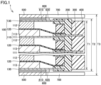
- Fig. 1 is a cross-sectional view schematically illustrating a power storage device according to an embodiment of the present disclosure.
- a power storage device 1 comprises an electrode stack 100, a sealing member 200, at least one inner voltage detection terminal 300, a housing 400, a pair of outer current collector plates 500, an electrically-conductive adhesive 600, a pair of outer voltage detection terminals 700, and an insulating member 800 (see Fig. 2 ).
- Electrode stack 100 has a plurality of bipolar electrodes 110, a plurality of separators 120, and a pair of outermost current collectors 130.
- Bipolar electrodes 110 are stacked on top of one another. Each bipolar electrode 110 has a current collector 111, a positive electrode active material layer 112, and a negative electrode active material layer 113.
- Current collector 111 is made of metal, for example.
- Current collector 111 is formed in a rectangular shape, for example.
- Positive electrode active material layer 112 is provided on one side (the lower side in Fig. 1 ) of current collector 111.
- Negative electrode active material layer 113 is provided on the other side (the upper side in Fig. 1 ) of current collector 111.
- Bipolar electrodes 110 are stacked in a manner that positive electrode active material layer 112 of one bipolar electrode 110 faces negative electrode active material layer 113 of another bipolar electrode 110 that is adjacent to the one bipolar electrode 110.
- Separator 120 is interposed between positive electrode active material layer 112 and negative electrode active material layer 113. Separator 120 has functions to allow ions to pass through itself and to insulate positive electrode active material layer 112 from negative electrode active material layer 113 for avoiding their direct contact.
- the thickness of separator 120 may be less than both the thickness of positive electrode active material layer 112 and the thickness of negative electrode active material layer 113.
- Each outermost current collector 130 is located outside of a set of the plurality of bipolar electrodes 110 in the stacking direction of the plurality of bipolar electrodes 110 (the vertical direction in Fig. 1 ).
- On one outermost current collector 130 only positive electrode active material layer 112 is provided facing negative electrode active material layer 113 of bipolar electrode 110 that is adjacent to this outermost current collector 130 with separator 120 present therebetween; and on the other outermost current collector 130, only negative electrode active material layer 113 is provided facing positive electrode active material layer 112 of bipolar electrode 110 that is adjacent to this outermost current collector 130 with separator 120 present therebetween.
- each bipolar electrode 110 serves as both the positive electrode of a cell and the negative electrode of an adjacent cell, and the plurality of cells are connected to each other in series.
- Sealing member 200 seals an inner space that is formed between a pair of current collectors that are adjacent to each other in the stacking direction.
- Sealing member 200 is made of an insulating member. Sealing member 200 supports an end, in a direction orthogonal to the stacking direction, of each of current collector 111, outermost current collector 130, and separator 120.
- the inner space is filled with an electrolyte solution.
- each cell of electrode stack 100 may be constituted of a so-called all-solid-state battery having a solid electrolyte. In this case, separator 120 is not present.
- Inner voltage detection terminal 300 is electrically connected to bipolar electrode 110 located on the inside of the pair of outermost current collectors 130 in the stacking direction. Specifically, inner voltage detection terminal 300 is connected to current collector 111 and sticks out from sealing member 200. In the present embodiment, at least one inner voltage detection terminal 300 comprises the same number of inner voltage detection terminal 300 as the number of current collector 111, and each inner voltage detection terminal 300 is connected to current collector 111. Alternatively, the number of inner voltage detection terminal 300 may be less than the number of current collector 111. In this case, one inner voltage detection terminal 300 is connected for a certain number of current collectors 111 aligned in the stacking direction.
- Inner voltage detection terminal 300 protrudes from sealing member 200 in a direction orthogonal to the stacking direction, for example.
- the thickness of inner voltage detection terminal 300 is approximately from 0.05 mm to 0.1 mm.
- Inner voltage detection terminal 300 is connected to a detection circuit (not illustrated).
- the inner voltage detection terminals 300 of which are present side by side the positions of inner voltage detection terminals 300 are not aligned in a direction orthogonal to the stacking direction.
- Housing 400 supports inner voltage detection terminal 300.
- Housing 400 is made of an insulating material.
- Housing 400 is secured to the outer side of sealing member 200 in a direction orthogonal to the stacking direction.
- the size of housing 400 is designed so that it is capable of supporting inner voltage detection terminal 300.
- a dimension T1 of housing 400 in the stacking direction is preferably designed to be equal to or less than a length T2 of sealing member 200 in the stacking direction.
- Dimension T1 of housing 400 in the stacking direction may be designed to be equal to or less than a distance T3 between the outer surfaces of the pair of outer voltage detection terminals 700 in the stacking direction.
- Each outer current collector plate 500 is located outside of electrode stack 100 in the stacking direction. More specifically, each outer current collector plate 500 is located outside of outermost current collector 130 in the stacking direction. As illustrated in Fig. 2 , each outer current collector plate 500 is formed in a rectangular shape, for example. The thickness of each outer current collector plate 500 is designed to be approximately from 0.5 mm to 3 mm.
- Electrically-conductive adhesive 600 is provided on the outer surface of outermost current collector 130 in the stacking direction.
- Each outer voltage detection terminal 700 is electrically connected to outermost current collector 130. More specifically, as illustrated in Fig. 1 and Fig. 3 , each outer voltage detection terminal 700 is electrically connected to outermost current collector 130 with electrically-conductive adhesive 600 present therebetween. That is, electrically-conductive adhesive 600 has a first adhesive part 610 that is electrically conductive and that connects outermost current collector 130 with outer current collector plate 500, as well as a second adhesive part 620 that is electrically conductive and that connects outermost current collector 130 with outer voltage detection terminal 700. Each outer voltage detection terminal 700 is connected to a detection circuit (not illustrated).
- each outer voltage detection terminal 700 may be the same as, or different from, the thickness of each outer current collector plate 500.
- the thickness of each outer voltage detection terminal 700 is simply required to be sufficient for maintaining enough rigidity to prevent the outer voltage detection terminal 700 from bending by its own weight, and, for example, it is approximately from 0.5 mm to 3 mm.
- the thickness of outer voltage detection terminal 700 is designed to be equal to or less than the thickness of outer current collector plate 500, for example.
- the outer surface of outer voltage detection terminal 700 in the stacking direction may be formed flush with the outer surface of outer current collector plate 500 in the stacking direction. This configuration makes it possible to avoid distance T3 from being larger than the distance between the outer surfaces of the pair of outer current collector plates 500 in the stacking direction.
- Each outer voltage detection terminal 700 protrudes from outer current collector plate 500, in the same direction as inner voltage detection terminal 300 protrudes from sealing member 200 (the direction to the right in Fig. 1 and Fig. 2 ).
- the width of outer voltage detection terminal 700 in a direction that is orthogonal to the direction in which outer voltage detection terminal 700 protrudes from outer current collector plate 500 as well as to the stacking direction is less than the width of outer current collector plate 500 in the same, orthogonal direction.
- Each outer voltage detection terminal 700 is located outside of sealing member 200 in the stacking direction. Each outer voltage detection terminal 700 is located outside of housing 400 in the stacking direction.
- Insulating member 800 is interposed between outer voltage detection terminal 700 and outer current collector plate 500. Insulating member 800 insulates outer current collector plate 500 from outer voltage detection terminal 700. Insulating member 800 is formed by insert molding, application of an electrically-insulating adhesive, and/or the like. In Fig. 2 , insulating member 800 is marked with oblique lines.
- a large current flows from electrode stack 100 through first adhesive part 610 toward outer current collector plate 500, and detection of the voltage of outermost current collector 130 by outer voltage detection terminal 700 is made possible by second adhesive part 620 interposed between outer voltage detection terminal 700 and outermost current collector 130. Passage of current from outer current collector plate 500 to outer voltage detection terminal 700 is interrupted by insulating member 800.
- each outer voltage detection terminal 700 is thicker than inner voltage detection terminal 300 so that bending of outer voltage detection terminal 700 by its own weight is reduced as compared to inner voltage detection terminal 300, and thereby outer voltage detection terminal 700 does not need to be supported by the housing; and, furthermore, dimension T1 of housing 400 in the stacking direction is equal to or less than distance T3 between the pair of outer voltage detection terminals 700 in the stacking direction, and thereby an increase in the size of power storage device 1 is avoided.
- a power storage device is composed of a stack of a plurality of power storage modules each comprising stacked cells and housing 400, these power storage modules aligned in the stacking direction are spaced from each other so as to avoid contact between adjacent power storage modules.
- insulating member 800 may be interposed between outer current collector plate 500 and a base end 710 of outer voltage detection terminal 700.
- insulating member 800 may be interposed between an end of outer current collector plate 500 to which outer voltage detection terminal 700 is connected (the end to the right in Fig. 6 ) and outer voltage detection terminal 700.
- insulating member 800 may have a covering portion 810 covering the end face of base end 710, as well as an interposed portion 820 interposed between outer current collector plate 500 and base end 710.
- outer voltage detection terminal 700 may be spaced from outer current collector plate 500. That is, outer current collector plate 500 may be insulated from outer voltage detection terminal 700 by the presence of space. In this case, insulating member 800 is not present. Also in this case, the distance between the outer surfaces of the pair of outer voltage detection terminals 700 is designed to be equal to or less than the distance between the outer surfaces of the pair of outer current collector plates 500.
- a power storage device comprising:
- each outer voltage detection terminal is thicker than the inner voltage detection terminal, and thereby the outer voltage detection terminal does not need to be supported by the housing; and, furthermore, the dimension of the housing in the stacking direction is equal to or less than the distance between the pair of outer voltage detection terminals in the stacking direction, and thereby an increase in the size of the power storage device is avoided.
- the power storage device further comprising a sealing member that seals an inner space formed between a pair of the current collectors that are adjacent to each other in the stacking direction, wherein
- the housing can more reliably support the inner voltage detection terminal, and an increase in the size of the power storage device is more reliably avoided.
- the power storage device according to Aspect 1 or 2, further comprising:
- the outer voltage detection terminal is electrically insulated from the outer current collector plate, and thereby a decrease in the accuracy of the voltage measurement at the detection circuit connected to the outer voltage detection terminal, which can occur due to a voltage drop caused by resistance of the first adhesive part, is reduced, as compared to when a relatively large current, which has flown from the electrode stack through the first adhesive part to the outer current collector plate, flows from the outer current collector plate to the outer voltage detection terminal.
- the power storage device according to Aspect 3, further comprising an insulating member interposed between the outer voltage detection terminal and the outer current collector plate.
- the power storage device according to any one of Aspects 3 to 5, wherein the distance between the pair of outer voltage detection terminals in the stacking direction is equal to or less than a distance between the pair of outermost current collectors in the stacking direction.
- the size of the power storage device in the stacking direction is decreased.
Landscapes
- Chemical & Material Sciences (AREA)
- Chemical Kinetics & Catalysis (AREA)
- Electrochemistry (AREA)
- General Chemical & Material Sciences (AREA)
- Engineering & Computer Science (AREA)
- Manufacturing & Machinery (AREA)
- Physics & Mathematics (AREA)
- General Physics & Mathematics (AREA)
- Connection Of Batteries Or Terminals (AREA)
- Secondary Cells (AREA)
- Sealing Battery Cases Or Jackets (AREA)
Abstract
Description
- This nonprovisional application is based on
Japanese Patent Application No. 2022-162052 filed on October 7, 2022 - The present disclosure relates to a power storage device.
-
Japanese Patent Laying-Open No. 2020-61221 - In the bipolar battery described in
Japanese Patent Laying-Open No. 2020-61221 - An object of the present disclosure is to provide a power storage device that can avoid an increase in size.
- A power storage device according to an aspect of the present disclosure comprises: an electrode stack comprising a plurality of bipolar electrodes stacked on top of one another and a pair of outermost current collectors located outside of a set of the plurality of bipolar electrodes in a stacking direction of the plurality of bipolar electrodes; at least one inner voltage detection terminal connected to at least one of the plurality of bipolar electrodes; a housing supporting at least one of the at least one inner voltage detection terminal; and a pair of outer voltage detection terminals electrically connected respectively to the pair of outermost current collectors, wherein each of the plurality of bipolar electrodes has: a current collector; a positive electrode active material layer provided on one side of the current collector; and a negative electrode active material layer provided on the other side of the current collector, the inner voltage detection terminal is electrically connected to the bipolar electrode, each of the pair of outer voltage detection terminals is thicker than the at least one inner voltage detection terminal, the housing is located between the pair of outer voltage detection terminals in the stacking direction, and a dimension of the housing in the stacking direction is equal to or less than a distance between the pair of outer voltage detection terminals in the stacking direction.
- The foregoing and other objects, features, aspects and advantages of the present disclosure will become more apparent from the following detailed description of the present disclosure when taken in conjunction with the accompanying drawings.
-
-
Fig. 1 is a cross-sectional view schematically illustrating a power storage device according to an embodiment of the present disclosure. -
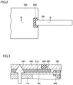
Fig. 2 is a plan view of an outer current collector plate, an outer voltage detection terminal, and an insulating member in a power storage device. -
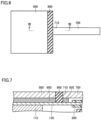
Fig. 3 is a cross-sectional view at Line III-III inFig. 2 . -
Fig. 4 is a plan view schematically illustrating a modification of the state of insulation between an outer current collector plate and an outer voltage detection terminal. -
Fig. 5 is a cross-sectional view at Line V-V inFig. 4 . -
Fig. 6 is a plan view schematically illustrating a modification of the state of insulation between an outer current collector plate and an outer voltage detection terminal. -
Fig. 7 is a cross-sectional view at Line VII-VII inFig. 6 . -
Fig. 8 is a plan view schematically illustrating a modification of the state of insulation between an outer current collector plate and an outer voltage detection terminal. -
Fig. 9 is a cross-sectional view at Line IX-IX inFig. 8 . -
Fig. 10 is a plan view schematically illustrating a modification of the state of insulation between an outer current collector plate and an outer voltage detection terminal. -
Fig. 11 is a cross-sectional view at Line XI-XI inFig. 10 . - A description will be given of an embodiment of the present disclosure, with reference to drawings. In the drawings referenced below, the same or equivalent members are denoted by the same numeral.
-
Fig. 1 is a cross-sectional view schematically illustrating a power storage device according to an embodiment of the present disclosure. As illustrated inFig. 1 , apower storage device 1 comprises anelectrode stack 100, asealing member 200, at least one innervoltage detection terminal 300, ahousing 400, a pair of outercurrent collector plates 500, an electrically-conductive adhesive 600, a pair of outervoltage detection terminals 700, and an insulating member 800 (seeFig. 2 ). -
Electrode stack 100 has a plurality of bipolar electrodes 110, a plurality ofseparators 120, and a pair of outermostcurrent collectors 130. - Bipolar electrodes 110 are stacked on top of one another. Each bipolar electrode 110 has a
current collector 111, a positive electrodeactive material layer 112, and a negative electrodeactive material layer 113. -
Current collector 111 is made of metal, for example.Current collector 111 is formed in a rectangular shape, for example. - Positive electrode
active material layer 112 is provided on one side (the lower side inFig. 1 ) ofcurrent collector 111. - Negative electrode
active material layer 113 is provided on the other side (the upper side inFig. 1 ) ofcurrent collector 111. - Bipolar electrodes 110 are stacked in a manner that positive electrode
active material layer 112 of one bipolar electrode 110 faces negative electrodeactive material layer 113 of another bipolar electrode 110 that is adjacent to the one bipolar electrode 110. -
Separator 120 is interposed between positive electrodeactive material layer 112 and negative electrodeactive material layer 113.Separator 120 has functions to allow ions to pass through itself and to insulate positive electrodeactive material layer 112 from negative electrodeactive material layer 113 for avoiding their direct contact. The thickness ofseparator 120 may be less than both the thickness of positive electrodeactive material layer 112 and the thickness of negative electrodeactive material layer 113. - Each outermost
current collector 130 is located outside of a set of the plurality of bipolar electrodes 110 in the stacking direction of the plurality of bipolar electrodes 110 (the vertical direction inFig. 1 ). On one outermostcurrent collector 130, only positive electrodeactive material layer 112 is provided facing negative electrodeactive material layer 113 of bipolar electrode 110 that is adjacent to this outermostcurrent collector 130 withseparator 120 present therebetween; and on the other outermostcurrent collector 130, only negative electrodeactive material layer 113 is provided facing positive electrodeactive material layer 112 of bipolar electrode 110 that is adjacent to this outermostcurrent collector 130 withseparator 120 present therebetween. - A pair of
current collectors 111 that are adjacent to each other in the stacking direction, in combination with positive electrodeactive material layer 112,separator 120, and negative electrodeactive material layer 113 located between the pair ofcurrent collectors 111, constitute a single cell. That is,electrode stack 100 is constituted of a plurality of cells stacked on top of one another; and the current collector disposed outside of the outermost cell, which is a cell among the plurality of cells that is located outermost in the stacking direction, constitutes outermostcurrent collector 130. - In a bipolar battery constituted of a plurality of cells stacked on top of one another, each bipolar electrode 110 serves as both the positive electrode of a cell and the negative electrode of an adjacent cell, and the plurality of cells are connected to each other in series.
- Sealing
member 200 seals an inner space that is formed between a pair of current collectors that are adjacent to each other in the stacking direction. Sealingmember 200 is made of an insulating member.Sealing member 200 supports an end, in a direction orthogonal to the stacking direction, of each ofcurrent collector 111, outermostcurrent collector 130, andseparator 120. In the present embodiment, the inner space is filled with an electrolyte solution. Alternatively, each cell ofelectrode stack 100 may be constituted of a so-called all-solid-state battery having a solid electrolyte. In this case,separator 120 is not present. - Inner
voltage detection terminal 300 is electrically connected to bipolar electrode 110 located on the inside of the pair of outermostcurrent collectors 130 in the stacking direction. Specifically, innervoltage detection terminal 300 is connected tocurrent collector 111 and sticks out from sealingmember 200. In the present embodiment, at least one innervoltage detection terminal 300 comprises the same number of innervoltage detection terminal 300 as the number ofcurrent collector 111, and each innervoltage detection terminal 300 is connected tocurrent collector 111. Alternatively, the number of innervoltage detection terminal 300 may be less than the number ofcurrent collector 111. In this case, one innervoltage detection terminal 300 is connected for a certain number ofcurrent collectors 111 aligned in the stacking direction. In other words, among a plurality ofcurrent collectors 111 aligned in the stacking direction, there may be acurrent collector 111 to which innervoltage detection terminal 300 is not connected. Innervoltage detection terminal 300 protrudes from sealingmember 200 in a direction orthogonal to the stacking direction, for example. The thickness of innervoltage detection terminal 300 is approximately from 0.05 mm to 0.1 mm. Innervoltage detection terminal 300 is connected to a detection circuit (not illustrated). As forcurrent collectors 111 the innervoltage detection terminals 300 of which are present side by side, the positions of innervoltage detection terminals 300 are not aligned in a direction orthogonal to the stacking direction. -
Housing 400 supports innervoltage detection terminal 300.Housing 400 is made of an insulating material.Housing 400 is secured to the outer side of sealingmember 200 in a direction orthogonal to the stacking direction. The size ofhousing 400 is designed so that it is capable of supporting innervoltage detection terminal 300. As illustrated inFig. 1 , a dimension T1 ofhousing 400 in the stacking direction is preferably designed to be equal to or less than a length T2 of sealingmember 200 in the stacking direction. Dimension T1 ofhousing 400 in the stacking direction may be designed to be equal to or less than a distance T3 between the outer surfaces of the pair of outervoltage detection terminals 700 in the stacking direction. - Each outer
current collector plate 500 is located outside ofelectrode stack 100 in the stacking direction. More specifically, each outercurrent collector plate 500 is located outside of outermostcurrent collector 130 in the stacking direction. As illustrated inFig. 2 , each outercurrent collector plate 500 is formed in a rectangular shape, for example. The thickness of each outercurrent collector plate 500 is designed to be approximately from 0.5 mm to 3 mm. - Electrically-
conductive adhesive 600 is provided on the outer surface of outermostcurrent collector 130 in the stacking direction. - Each outer
voltage detection terminal 700 is electrically connected to outermostcurrent collector 130. More specifically, as illustrated inFig. 1 andFig. 3 , each outervoltage detection terminal 700 is electrically connected to outermostcurrent collector 130 with electrically-conductive adhesive 600 present therebetween. That is, electrically-conductive adhesive 600 has a firstadhesive part 610 that is electrically conductive and that connects outermostcurrent collector 130 with outercurrent collector plate 500, as well as a secondadhesive part 620 that is electrically conductive and that connects outermostcurrent collector 130 with outervoltage detection terminal 700. Each outervoltage detection terminal 700 is connected to a detection circuit (not illustrated). - The thickness of each outer
voltage detection terminal 700 may be the same as, or different from, the thickness of each outercurrent collector plate 500. The thickness of each outervoltage detection terminal 700 is simply required to be sufficient for maintaining enough rigidity to prevent the outervoltage detection terminal 700 from bending by its own weight, and, for example, it is approximately from 0.5 mm to 3 mm. The thickness of outervoltage detection terminal 700 is designed to be equal to or less than the thickness of outercurrent collector plate 500, for example. The outer surface of outervoltage detection terminal 700 in the stacking direction may be formed flush with the outer surface of outercurrent collector plate 500 in the stacking direction. This configuration makes it possible to avoid distance T3 from being larger than the distance between the outer surfaces of the pair of outercurrent collector plates 500 in the stacking direction. - Each outer
voltage detection terminal 700 protrudes from outercurrent collector plate 500, in the same direction as innervoltage detection terminal 300 protrudes from sealing member 200 (the direction to the right inFig. 1 andFig. 2 ). As illustrated inFig. 2 , the width of outervoltage detection terminal 700 in a direction that is orthogonal to the direction in which outervoltage detection terminal 700 protrudes from outercurrent collector plate 500 as well as to the stacking direction (namely, in the vertical direction inFig. 2 ) is less than the width of outercurrent collector plate 500 in the same, orthogonal direction. - Each outer
voltage detection terminal 700 is located outside of sealingmember 200 in the stacking direction. Each outervoltage detection terminal 700 is located outside ofhousing 400 in the stacking direction. - Insulating
member 800 is interposed between outervoltage detection terminal 700 and outercurrent collector plate 500. Insulatingmember 800 insulates outercurrent collector plate 500 from outervoltage detection terminal 700. Insulatingmember 800 is formed by insert molding, application of an electrically-insulating adhesive, and/or the like. InFig. 2 , insulatingmember 800 is marked with oblique lines. - In the direction indicated by an arrow AR1 in
Fig. 3 , a large current flows fromelectrode stack 100 through firstadhesive part 610 toward outercurrent collector plate 500, and detection of the voltage of outermostcurrent collector 130 by outervoltage detection terminal 700 is made possible by secondadhesive part 620 interposed between outervoltage detection terminal 700 and outermostcurrent collector 130. Passage of current from outercurrent collector plate 500 to outervoltage detection terminal 700 is interrupted by insulatingmember 800. - As described above, in
power storage device 1 according to the present embodiment, each outervoltage detection terminal 700 is thicker than innervoltage detection terminal 300 so that bending of outervoltage detection terminal 700 by its own weight is reduced as compared to innervoltage detection terminal 300, and thereby outervoltage detection terminal 700 does not need to be supported by the housing; and, furthermore, dimension T1 ofhousing 400 in the stacking direction is equal to or less than distance T3 between the pair of outervoltage detection terminals 700 in the stacking direction, and thereby an increase in the size ofpower storage device 1 is avoided. - Moreover, in a case when a power storage device is composed of a stack of a plurality of power storage modules each comprising stacked cells and
housing 400, these power storage modules aligned in the stacking direction are spaced from each other so as to avoid contact between adjacent power storage modules. Because of this, when dimension T1 ofhousing 400 in the stacking direction is more than distance T3 between the pair of outervoltage detection terminals 700 in the stacking direction, the thickness of outercurrent collector plate 500 interposed between adjacent power storage modules increases; on the other hand, inpower storage device 1 according to the present embodiment, where dimension T1 ofhousing 400 in the stacking direction is equal to or less than distance T3 between the pair of outervoltage detection terminals 700 in the stacking direction, an increase in the thickness of outercurrent collector plate 500 is avoided and thereby an increase in the total size of the power storage device is avoided. - In this embodiment, as illustrated in
Fig. 4 and Fig. 5 , insulatingmember 800 may be interposed between outercurrent collector plate 500 and abase end 710 of outervoltage detection terminal 700. - As illustrated in
Fig. 6 and Fig. 7 , insulatingmember 800 may be interposed between an end of outercurrent collector plate 500 to which outervoltage detection terminal 700 is connected (the end to the right inFig. 6 ) and outervoltage detection terminal 700. - As illustrated in
Fig. 8 and Fig. 9 , when electrically-conductive adhesive 600 is formed thicker than outervoltage detection terminal 700,base end 710 of outervoltage detection terminal 700 may be buried inside electrically-conductive adhesive 600 through insulatingmember 800. That is, insulatingmember 800 may have a coveringportion 810 covering the end face ofbase end 710, as well as an interposedportion 820 interposed between outercurrent collector plate 500 andbase end 710. - As illustrated in
Fig. 10 and Fig. 11 , outervoltage detection terminal 700 may be spaced from outercurrent collector plate 500. That is, outercurrent collector plate 500 may be insulated from outervoltage detection terminal 700 by the presence of space. In this case, insulatingmember 800 is not present. Also in this case, the distance between the outer surfaces of the pair of outervoltage detection terminals 700 is designed to be equal to or less than the distance between the outer surfaces of the pair of outercurrent collector plates 500. - A person skilled in the art will appreciate that the above-described example embodiment is a specific example of the following aspects.
- A power storage device comprising:
- an electrode stack comprising:
- a plurality of bipolar electrodes stacked on top of one another; and
- a pair of outermost current collectors located outside of a set of the plurality of bipolar electrodes in a stacking direction of the plurality of bipolar electrodes;
- at least one inner voltage detection terminal connected to at least one of the plurality of bipolar electrodes;
- a housing supporting at least one of the at least one inner voltage detection terminal; and
- a pair of outer voltage detection terminals electrically connected respectively to the pair of outermost current collectors, wherein
- each of the plurality of bipolar electrodes has:
- a current collector;
- a positive electrode active material layer provided on one side of the current collector; and
- a negative electrode active material layer provided on the other side of the current collector,
- the at least one inner voltage detection terminal is electrically connected to the bipolar electrode,
- each of the pair of outer voltage detection terminals is thicker than the at least one inner voltage detection terminal,
- the housing is located between the pair of outer voltage detection terminals in the stacking direction, and
- a dimension of the housing in the stacking direction is equal to or less than a distance between the pair of outer voltage detection terminals in the stacking direction.
- In this power storage device, each outer voltage detection terminal is thicker than the inner voltage detection terminal, and thereby the outer voltage detection terminal does not need to be supported by the housing; and, furthermore, the dimension of the housing in the stacking direction is equal to or less than the distance between the pair of outer voltage detection terminals in the stacking direction, and thereby an increase in the size of the power storage device is avoided.
- The power storage device according to
Aspect 1, further comprising a sealing member that seals an inner space formed between a pair of the current collectors that are adjacent to each other in the stacking direction, wherein - the sealing member is located between the pair of outer voltage detection terminals, and
- the dimension of the housing in the stacking direction is equal to or less than a length of the sealing member in the stacking direction.
- In this aspect, the housing can more reliably support the inner voltage detection terminal, and an increase in the size of the power storage device is more reliably avoided.
- The power storage device according to
Aspect 1 or 2, further comprising: - an outer current collector plate located on an outside of the electrode stack in the stacking direction;
- a first adhesive part that is electrically conductive and connects the outermost current collector with the outer current collector plate; and
- a second adhesive part that is electrically conductive and connects the outermost current collector with the outer voltage detection terminal, wherein
- the outer voltage detection terminal is electrically insulated from the outer current collector plate.
- In this aspect, the outer voltage detection terminal is electrically insulated from the outer current collector plate, and thereby a decrease in the accuracy of the voltage measurement at the detection circuit connected to the outer voltage detection terminal, which can occur due to a voltage drop caused by resistance of the first adhesive part, is reduced, as compared to when a relatively large current, which has flown from the electrode stack through the first adhesive part to the outer current collector plate, flows from the outer current collector plate to the outer voltage detection terminal.
- The power storage device according to Aspect 3, further comprising an insulating member interposed between the outer voltage detection terminal and the outer current collector plate.
- The power storage device according to Aspect 3, wherein the outer voltage detection terminal is spaced from the outer current collector plate.
- The power storage device according to any one of Aspects 3 to 5, wherein the distance between the pair of outer voltage detection terminals in the stacking direction is equal to or less than a distance between the pair of outermost current collectors in the stacking direction.
- In this aspect, as compared to when all the detection terminals are supported by the housing, the size of the power storage device in the stacking direction is decreased.
- Although the embodiments of the present disclosure have been described, the embodiments disclosed herein are illustrative and non-restrictive in any respect. The scope of the present disclosure is defined by the terms of the claims, and is intended to encompass any modifications within the meaning and the scope equivalent to the terms of the claims.
Claims (6)
- A power storage device (1) comprising:an electrode stack (100) comprising:a plurality of bipolar electrodes (110) stacked on top of one another; anda pair of outermost current collectors (130) located outside of a set of the plurality of bipolar electrodes in a stacking direction of the plurality of bipolar electrodes;at least one inner voltage detection terminal (300) connected to at least one of the plurality of bipolar electrodes;a housing (400) supporting at least one of the at least one inner voltage detection terminal; anda pair of outer voltage detection terminals (700) electrically connected respectively to the pair of outermost current collectors, whereineach of the plurality of bipolar electrodes has:a current collector (111);a positive electrode active material layer (112) provided on one side of the current collector; anda negative electrode active material layer (113) provided on the other side of the current collector,the inner voltage detection terminal is electrically connected to the bipolar electrode,each of the pair of outer voltage detection terminals is thicker than the at least one inner voltage detection terminal,the housing is located between the pair of outer voltage detection terminals in the stacking direction, anda dimension (T1) of the housing in the stacking direction is equal to or less than a distance (T3) between the pair of outer voltage detection terminals in the stacking direction.
- The power storage device according to claim 1, further comprising a sealing member (200) that seals an inner space formed between a pair of the current collectors that are adjacent to each other in the stacking direction, whereinthe sealing member is located between the pair of outer voltage detection terminals, andthe dimension of the housing in the stacking direction is equal to or less than a length (T2) of the sealing member in the stacking direction.
- The power storage device according to claim 1 or 2, further comprising:an outer current collector plate (500) located on an outside of the electrode stack in the stacking direction;a first adhesive part (610) that is electrically conductive and connects the outermost current collector with the outer current collector plate; anda second adhesive part (620) that is electrically conductive and connects the outermost current collector with the outer voltage detection terminal, whereinthe outer voltage detection terminal is electrically insulated from the outer current collector plate.
- The power storage device according to claim 3, further comprising an insulating member (800) interposed between the outer voltage detection terminal and the outer current collector plate.
- The power storage device according to claim 3, wherein the outer voltage detection terminal is spaced from the outer current collector plate.
- The power storage device according to claim 3, wherein the distance between the pair of outer voltage detection terminals in the stacking direction is equal to or less than a distance between the pair of outermost current collectors in the stacking direction.
Applications Claiming Priority (1)
| Application Number | Priority Date | Filing Date | Title |
|---|---|---|---|
| JP2022162052A JP2024055266A (en) | 2022-10-07 | 2022-10-07 | Power storage device |
Publications (2)
| Publication Number | Publication Date |
|---|---|
| EP4350826A2 true EP4350826A2 (en) | 2024-04-10 |
| EP4350826A3 EP4350826A3 (en) | 2024-08-14 |
Family
ID=88241353
Family Applications (1)
| Application Number | Title | Priority Date | Filing Date |
|---|---|---|---|
| EP23201436.5A Pending EP4350826A3 (en) | 2022-10-07 | 2023-10-03 | Power storage device |
Country Status (5)
| Country | Link |
|---|---|
| US (1) | US20240120627A1 (en) |
| EP (1) | EP4350826A3 (en) |
| JP (1) | JP2024055266A (en) |
| KR (1) | KR20240049152A (en) |
| CN (1) | CN117855554A (en) |
Citations (1)
| Publication number | Priority date | Publication date | Assignee | Title |
|---|---|---|---|---|
| JP2020061221A (en) | 2018-10-05 | 2020-04-16 | 日産自動車株式会社 | Bipolar secondary battery |
Family Cites Families (2)
| Publication number | Priority date | Publication date | Assignee | Title |
|---|---|---|---|---|
| JP4238645B2 (en) * | 2003-06-12 | 2009-03-18 | 日産自動車株式会社 | Bipolar battery |
| JP7359098B2 (en) * | 2020-07-31 | 2023-10-11 | 株式会社豊田自動織機 | Energy storage module |
-
2022
- 2022-10-07 JP JP2022162052A patent/JP2024055266A/en active Pending
-
2023
- 2023-08-28 US US18/456,685 patent/US20240120627A1/en active Pending
- 2023-09-15 KR KR1020230123097A patent/KR20240049152A/en active Pending
- 2023-09-27 CN CN202311256952.5A patent/CN117855554A/en active Pending
- 2023-10-03 EP EP23201436.5A patent/EP4350826A3/en active Pending
Patent Citations (1)
| Publication number | Priority date | Publication date | Assignee | Title |
|---|---|---|---|---|
| JP2020061221A (en) | 2018-10-05 | 2020-04-16 | 日産自動車株式会社 | Bipolar secondary battery |
Also Published As
| Publication number | Publication date |
|---|---|
| US20240120627A1 (en) | 2024-04-11 |
| CN117855554A (en) | 2024-04-09 |
| EP4350826A3 (en) | 2024-08-14 |
| KR20240049152A (en) | 2024-04-16 |
| JP2024055266A (en) | 2024-04-18 |
Similar Documents
| Publication | Publication Date | Title |
|---|---|---|
| US12294059B1 (en) | Battery with discontinuous bond layer | |
| KR102372383B1 (en) | A battery module having a structure with an improved energy density, a battery pack and a vehicle comprising the same | |
| US11600891B1 (en) | Battery configurations having balanced current collectors | |
| KR100823193B1 (en) | Secondary battery | |
| CN116247384A (en) | battery stack | |
| KR20080019311A (en) | Pouch type secondary battery improves safety by preventing internal flow of electrode assembly | |
| KR20230092218A (en) | Battery module with electrolyte leakage detection function and battery pack comprising the same | |
| KR20140104435A (en) | Electrical energy storage module and method for producing an electrical energy storage module | |
| EP2874204B1 (en) | Battery assembly | |
| KR20180093330A (en) | Battery Pack Comprising Electrode Terminal Connecting Plate | |
| KR20180082785A (en) | Device Comprising Member for Preventing Short-Circuit for Measuring Electrode Potential by Using Three Electrode System | |
| US20240213625A1 (en) | Cell laminate | |
| US20240097266A1 (en) | Battery assembly and method therefor | |
| CN116632429A (en) | Square cell power battery system | |
| CN107210390A (en) | Battery list pond and battery system | |
| US20240213514A1 (en) | Power storage module | |
| US20240120627A1 (en) | Power storage device | |
| EP4415080A1 (en) | Power storage device | |
| KR20180105306A (en) | Apparatus for Charging and Discharging Battery Cell Comprising Insulation Mask | |
| JP7262637B1 (en) | bipolar battery | |
| CN220963421U (en) | Battery cell, battery assembly and device | |
| US20260142307A1 (en) | Battery module and battery pack comprising the same | |
| CN223487089U (en) | Non-aqueous lithium-ion secondary batteries | |
| EP4589695A2 (en) | Electrode plate, electrode assembly and rechargeable battery including the electrode assembly | |
| KR20040058922A (en) | Prismatic type lithium secondary battery |
Legal Events
| Date | Code | Title | Description |
|---|---|---|---|
| PUAI | Public reference made under article 153(3) epc to a published international application that has entered the european phase |
Free format text: ORIGINAL CODE: 0009012 |
|
| STAA | Information on the status of an ep patent application or granted ep patent |
Free format text: STATUS: REQUEST FOR EXAMINATION WAS MADE |
|
| 17P | Request for examination filed |
Effective date: 20231021 |
|
| AK | Designated contracting states |
Kind code of ref document: A2 Designated state(s): AL AT BE BG CH CY CZ DE DK EE ES FI FR GB GR HR HU IE IS IT LI LT LU LV MC ME MK MT NL NO PL PT RO RS SE SI SK SM TR |
|
| PUAL | Search report despatched |
Free format text: ORIGINAL CODE: 0009013 |
|
| AK | Designated contracting states |
Kind code of ref document: A3 Designated state(s): AL AT BE BG CH CY CZ DE DK EE ES FI FR GB GR HR HU IE IS IT LI LT LU LV MC ME MK MT NL NO PL PT RO RS SE SI SK SM TR |
|
| RIC1 | Information provided on ipc code assigned before grant |
Ipc: G01R 31/396 20190101ALI20240711BHEP Ipc: G01R 31/382 20190101ALI20240711BHEP Ipc: H01M 4/02 20060101ALI20240711BHEP Ipc: H01M 4/70 20060101ALI20240711BHEP Ipc: H01M 50/55 20210101ALI20240711BHEP Ipc: H01M 50/54 20210101ALI20240711BHEP Ipc: H01M 50/536 20210101ALI20240711BHEP Ipc: H01M 10/0585 20100101ALI20240711BHEP Ipc: H01M 50/569 20210101ALI20240711BHEP Ipc: H01M 50/543 20210101ALI20240711BHEP Ipc: H01M 50/186 20210101ALI20240711BHEP Ipc: H01M 10/48 20060101ALI20240711BHEP Ipc: H01M 10/04 20060101AFI20240711BHEP |