EP4350769A1 - An electrostatic discharge, esd, protection semiconductor device for providing esd protection between a first and a second terminal of another semiconductor device, as well as a corresponding metal oxide semiconductor, mos, field effect transistor, fet, and a related method - Google Patents
An electrostatic discharge, esd, protection semiconductor device for providing esd protection between a first and a second terminal of another semiconductor device, as well as a corresponding metal oxide semiconductor, mos, field effect transistor, fet, and a related method Download PDFInfo
- Publication number
- EP4350769A1 EP4350769A1 EP22200290.9A EP22200290A EP4350769A1 EP 4350769 A1 EP4350769 A1 EP 4350769A1 EP 22200290 A EP22200290 A EP 22200290A EP 4350769 A1 EP4350769 A1 EP 4350769A1
- Authority
- EP
- European Patent Office
- Prior art keywords
- esd
- region
- semiconductor device
- terminal
- diode region
- Prior art date
- Legal status (The legal status is an assumption and is not a legal conclusion. Google has not performed a legal analysis and makes no representation as to the accuracy of the status listed.)
- Granted
Links
Images


Classifications
-
- H—ELECTRICITY
- H10—SEMICONDUCTOR DEVICES; ELECTRIC SOLID-STATE DEVICES NOT OTHERWISE PROVIDED FOR
- H10D—INORGANIC ELECTRIC SEMICONDUCTOR DEVICES
- H10D89/00—Aspects of integrated devices not covered by groups H10D84/00 - H10D88/00
- H10D89/60—Integrated devices comprising arrangements for electrical or thermal protection, e.g. protection circuits against electrostatic discharge [ESD]
-
- H—ELECTRICITY
- H10—SEMICONDUCTOR DEVICES; ELECTRIC SOLID-STATE DEVICES NOT OTHERWISE PROVIDED FOR
- H10D—INORGANIC ELECTRIC SEMICONDUCTOR DEVICES
- H10D30/00—Field-effect transistors [FET]
- H10D30/60—Insulated-gate field-effect transistors [IGFET]
-
- H—ELECTRICITY
- H10—SEMICONDUCTOR DEVICES; ELECTRIC SOLID-STATE DEVICES NOT OTHERWISE PROVIDED FOR
- H10D—INORGANIC ELECTRIC SEMICONDUCTOR DEVICES
- H10D30/00—Field-effect transistors [FET]
- H10D30/60—Insulated-gate field-effect transistors [IGFET]
- H10D30/64—Double-diffused metal-oxide semiconductor [DMOS] FETs
- H10D30/66—Vertical DMOS [VDMOS] FETs
- H10D30/668—Vertical DMOS [VDMOS] FETs having trench gate electrodes, e.g. UMOS transistors
-
- H—ELECTRICITY
- H10—SEMICONDUCTOR DEVICES; ELECTRIC SOLID-STATE DEVICES NOT OTHERWISE PROVIDED FOR
- H10D—INORGANIC ELECTRIC SEMICONDUCTOR DEVICES
- H10D84/00—Integrated devices formed in or on semiconductor substrates that comprise only semiconducting layers, e.g. on Si wafers or on GaAs-on-Si wafers
- H10D84/01—Manufacture or treatment
-
- H—ELECTRICITY
- H10—SEMICONDUCTOR DEVICES; ELECTRIC SOLID-STATE DEVICES NOT OTHERWISE PROVIDED FOR
- H10D—INORGANIC ELECTRIC SEMICONDUCTOR DEVICES
- H10D84/00—Integrated devices formed in or on semiconductor substrates that comprise only semiconducting layers, e.g. on Si wafers or on GaAs-on-Si wafers
- H10D84/101—Integrated devices comprising main components and built-in components, e.g. IGBT having built-in freewheel diode
- H10D84/141—VDMOS having built-in components
- H10D84/143—VDMOS having built-in components the built-in components being PN junction diodes
-
- H—ELECTRICITY
- H10—SEMICONDUCTOR DEVICES; ELECTRIC SOLID-STATE DEVICES NOT OTHERWISE PROVIDED FOR
- H10D—INORGANIC ELECTRIC SEMICONDUCTOR DEVICES
- H10D89/00—Aspects of integrated devices not covered by groups H10D84/00 - H10D88/00
- H10D89/60—Integrated devices comprising arrangements for electrical or thermal protection, e.g. protection circuits against electrostatic discharge [ESD]
- H10D89/601—Integrated devices comprising arrangements for electrical or thermal protection, e.g. protection circuits against electrostatic discharge [ESD] for devices having insulated gate electrodes, e.g. for IGFETs or IGBTs
- H10D89/611—Integrated devices comprising arrangements for electrical or thermal protection, e.g. protection circuits against electrostatic discharge [ESD] for devices having insulated gate electrodes, e.g. for IGFETs or IGBTs using diodes as protective elements
-
- H—ELECTRICITY
- H10—SEMICONDUCTOR DEVICES; ELECTRIC SOLID-STATE DEVICES NOT OTHERWISE PROVIDED FOR
- H10D—INORGANIC ELECTRIC SEMICONDUCTOR DEVICES
- H10D89/00—Aspects of integrated devices not covered by groups H10D84/00 - H10D88/00
- H10D89/60—Integrated devices comprising arrangements for electrical or thermal protection, e.g. protection circuits against electrostatic discharge [ESD]
- H10D89/601—Integrated devices comprising arrangements for electrical or thermal protection, e.g. protection circuits against electrostatic discharge [ESD] for devices having insulated gate electrodes, e.g. for IGFETs or IGBTs
- H10D89/811—Integrated devices comprising arrangements for electrical or thermal protection, e.g. protection circuits against electrostatic discharge [ESD] for devices having insulated gate electrodes, e.g. for IGFETs or IGBTs using FETs as protective elements
-
- H—ELECTRICITY
- H10—SEMICONDUCTOR DEVICES; ELECTRIC SOLID-STATE DEVICES NOT OTHERWISE PROVIDED FOR
- H10D—INORGANIC ELECTRIC SEMICONDUCTOR DEVICES
- H10D89/00—Aspects of integrated devices not covered by groups H10D84/00 - H10D88/00
- H10D89/60—Integrated devices comprising arrangements for electrical or thermal protection, e.g. protection circuits against electrostatic discharge [ESD]
- H10D89/601—Integrated devices comprising arrangements for electrical or thermal protection, e.g. protection circuits against electrostatic discharge [ESD] for devices having insulated gate electrodes, e.g. for IGFETs or IGBTs
- H10D89/921—Integrated devices comprising arrangements for electrical or thermal protection, e.g. protection circuits against electrostatic discharge [ESD] for devices having insulated gate electrodes, e.g. for IGFETs or IGBTs characterised by the configuration of the interconnections connecting the protective arrangements, e.g. ESD buses
-
- H—ELECTRICITY
- H10—SEMICONDUCTOR DEVICES; ELECTRIC SOLID-STATE DEVICES NOT OTHERWISE PROVIDED FOR
- H10D—INORGANIC ELECTRIC SEMICONDUCTOR DEVICES
- H10D89/00—Aspects of integrated devices not covered by groups H10D84/00 - H10D88/00
- H10D89/60—Integrated devices comprising arrangements for electrical or thermal protection, e.g. protection circuits against electrostatic discharge [ESD]
- H10D89/601—Integrated devices comprising arrangements for electrical or thermal protection, e.g. protection circuits against electrostatic discharge [ESD] for devices having insulated gate electrodes, e.g. for IGFETs or IGBTs
- H10D89/931—Integrated devices comprising arrangements for electrical or thermal protection, e.g. protection circuits against electrostatic discharge [ESD] for devices having insulated gate electrodes, e.g. for IGFETs or IGBTs characterised by the dispositions of the protective arrangements
-
- H—ELECTRICITY
- H10—SEMICONDUCTOR DEVICES; ELECTRIC SOLID-STATE DEVICES NOT OTHERWISE PROVIDED FOR
- H10W—GENERIC PACKAGES, INTERCONNECTIONS, CONNECTORS OR OTHER CONSTRUCTIONAL DETAILS OF DEVICES COVERED BY CLASS H10
- H10W72/00—Interconnections or connectors in packages
- H10W72/20—Bump connectors, e.g. solder bumps or copper pillars; Dummy bumps; Thermal bumps
Definitions
- the present disclosure relates to the field of Electrostatic Discharge, ESD, protection and, more in particular, to an ESD protection semiconductor device implemented in a semiconductor material.
- a Trench Gate Metal Oxide Semiconductor, MOS, Field Effect Transistor, FET typically comprises a source region towards a first major surface of the MOSFET and a drain region formed on a second major surface, opposite to the first major surface.
- the source and drain region have the same conductivity type.
- a channel-accommodating region i.e. a body region, is provided between the source and drain region, which channel-accommodating region is of a different conductivity type to that of the source and drain region.
- a conductive channel is to be construed between the source region and the drain region to assure that the MOSFET is turned on.
- a trench gate electrode is provided close to, but not in electrical contact with, the channel-accommodating region.
- Typical for the trench gate MOSFET is that the current is conducted vertically from one surface to the other so as to achieve a high drive capability. It may be realized by packing trenches on a chip, deep enough to cross the oppositely doped body region, i.e. channel-accommodating region, below the top surface.
- the gate trench is typically provided with some sort of oxide, to assure that the gate electrode is electrically isolated from the channel-accommodating region. Providing a voltage bias at the gate trench will then produce an electrical field which extends into, and thus also locally depletes and/or inverts, the channel-accommodating region.
- Trench gate MOSFETs are able to cope with high voltage operations, for example in the region of 100V or above.
- MOSFETs may be able to cope with high reverse bias voltages between the source region and the drain region, without that the MOSFET will break down of pass any significant reverse current.
- the above is typically achieved by introducing a drift region between the drain region and the channel-accommodating region, wherein the drift region has the same conductivity type as the source region and the drain region.
- the drift region typically has a lower doping concentration.
- the drain region forms a PN junction at the interface with the channel-accommodating region which serves to block the reverse bias current.
- the drain region is positive relative to the source region. If the source region is positive relative to the drain region, then the body-drain junction may become biased and current may be conducted via the drain region and the source region. Alternatively, for P-channel MOSFETs, the drain region is negative relative to the source region. If the source region is negative relative to the drain region, then the body-drain junction may again conduct current.
- the breakdown voltage is dependent on the thickness of the drift region wherein the greater the thickness, the higher the breakdown voltage.
- the channel regions are designed along the vertical walls of the trenches, rather than laterally. This allows for a high density of channels, i.e. two for each trench, per unit area of the device.
- MOSFETs may be prone Electrostatic Discharge, ESD. The same is applicable for other type of semiconductor devices.
- MOSFET Metal Oxide Semiconductor, MOS, Field Effect Transistor, FET, MOSFET, wherein the MOSFET further comprises an ESD protection semiconductor device in accordance with the present disclosure.
- An Electrostatic Discharge, ESD, protection semiconductor device for providing ESD protection between a first and a second terminal of another semiconductor device, the ESD protection device comprising a semiconductor body having a first major surface, wherein the semiconductor device further comprises a first ESD terminal arranged to be connected to a first terminal of the other semiconductor device, a second ESD terminal arranged to be connected to a second terminal of the other semiconductor device, and a floating terminal, and wherein the semiconductor body further comprises:
- the present disclosure has several advantages over more traditional ESD protection.
- the inventors have found that it may be beneficial to incorporate ESD protection in the semiconductor body. That is, the diodes are actually implemented in the semiconductor body, for example in silicon material. This may ensure that the leakage current is relatively low, for example a couple of nano Ampere.
- said ESD protection semiconductor device is elongated, and wherein said floating terminal comprises individual, electrically isolated, floating strips for providing connections between said second diode region and said third diode region.
- the main advantage of this aspect is that the active area of the semiconductor material is improved.
- the span of the diodes may be reduced, for example to about 14,5 ⁇ m, as will be apparent later when referring to the figures.
- the introduction of the new design for the floating terminal fulfils different design rules that need to be considered when designing ESD protection.
- the present disclosure discloses creating individual, electrically, isolated floating strips. This means that those strips will not “cover” the entire span of the elongated ESD protection semiconductor device.
- the space in between subsequent floating strips may be utilized for connection to the first and/or second terminal of the another semiconductor device. This is beneficial for reducing the size of the ESD protection semiconductor device, and thus for improving the active area.
- the above described ESD semiconductor device effectively establishes the introduction of four back to back diodes between the first terminal and the second terminal of the another semiconductor device, as there are four interfaces or boundaries between two semiconductor material types.
- the diodes are oriented in that the cathodes of the diodes are connected to each other. This is accomplished by the layout of the ESD region and the specific diode regions inside that corresponding ESD region.
- the first conductivity type is N-type
- the second conductivity type is P-type, or vice-versa.
- the ESD protection device may be especially useful for protecting a 12Volt gate to source voltage of a MOSFET.
- even more diodes may be utilized in the design. So, six, eight, or even ten diodes may be used instead of the four diodes.
- the present disclosure is thus not limited to four diodes, but to at least four diodes.
- the ESD protection device comprises a first, a second and a third isolating trench, wherein each of said three trenches extend into the semiconductor body from the major surface, and wherein said first ESD region is oriented between said first and second isolating trench and wherein said second ESD region is oriented between said second and third isolating trench.
- the inventors have found that it might be beneficial to introduce isolating trenches to ensure that the functioning of the ESD protection semiconductor device does not influence the functioning of the another semiconductor device.
- Another option is to introduce isolating regions, for example by sacrificing area of the semiconductor material or by a different form of isolation material or design or the like.
- the isolating trenches may, for example, be provided with oxide material or any other type of isolating material.
- a shape of said ESD semiconductor device is a geometric shape thereby enclosing a semiconductor material of said semiconductor body.
- the enclosed semiconductor material is to be connected to said first terminal of said another semiconductor device.
- the above described example provides for a relatively robust ESD protection for the another semiconductor device.
- the another semiconductor device may be manufactured in such a way that its first terminal is aligned with the enclosed semiconductor material of the ESD semiconductor device. This allows for an effective ESD protection.
- first, second, third and fourth diode regions are each endless loops, seen in said top view, surrounding a central region of semiconductor material forming the first ESD terminal.
- the above may entail that there is no end face of the ESD protection semiconductor device, but that the ESD protection semiconductor device is construed in such a way that there is effectively no beginning or end, just like a circle.
- the above described example provides for an effective way of protecting a MOSFET, wherein the first terminal is the gate terminal of the MOSFET and the second terminal if the source terminal of the MOSFET.
- MOSFET Metal Oxide Semiconductor, MOS, Field Effect Transistor, FET, MOSFET, having a gate pad and a source pad embodied in a semiconductor material, wherein said MOSFET further comprises an Electrostatic Discharge, ESD, protection semiconductor device in accordance with any of the previous examples.
- the ESD protection device is aligned with said gate pad of said MOSFET.
- the method further comprises the step of:
- the ESD protection semiconductor device is formed such that in said top view of said ESD protection semiconductor device, a shape of said ESD protection semiconductor device is a geometric shape thereby enclosing a semiconductor material of said semiconductor body.
- the ESD protection semiconductor device is formed such that the first, second, third and fourth diode regions are each endless loops, seen in said top view, surrounding a central region of semiconductor material forming the first ESD terminal.
- the ESD protection semiconductor device is formed such that, in said top view of said ESD protection semiconductor device:
- the words “comprise,” “comprising,” and the like are to be construed in an inclusive sense, as opposed to an exclusive or exhaustive sense; that is to say, in the sense of "including, but not limited to.”
- the terms “connected,” “coupled,” or any variant thereof means any connection or coupling, either direct or indirect, between two or more elements; the coupling or connection between the elements can be physical, logical, electromagnetic, or a combination thereof.
- the words “herein,” “above,” “below,” and words of similar import when used in this application, refer to this application as a whole and not to any particular portions of this application.
- words in the Detailed Description using the singular or plural number may also include the plural or singular number respectively.
- the word "or,” in reference to a list of two or more items, covers all of the following interpretations of the word: any of the items in the list, all of the items in the list, and any combination of the items in the list.
- Figure 1 discloses Electro Static Discharge, ESD, protection for a Metal oxide Semiconductor, MOS, Field Effect Transistor, FET 1 having a source 4, a drain 2 and a gate 3 terminal.
- Junction damage may be caused by the injection of an ESD transient of sufficient energy and duration to force the junction into secondary breakdown. Junction damage is often characterized by high reverse bias leakage current or a total short.
- gate oxide damage may occur when the gate 3 is subjected to an ESD pulse of high enough magnitude to cause the gate oxide to breakdown.
- the gate oxide is typically very thin resulting in varying degrees of ESD sensitivity.
- Metallization burnout may exist in metal interconnects or contacts. It may occur if any current flowing through the metal forces a temperature rise that is high enough to reach the melting point of the material. Metallization burnout is often a secondary effect, occurring after the initial junction or gate oxide failure.
- the main objective is typically to clamp the gate 3 to source 4 voltage from reaching the destructive voltage.
- a typical ESD protection device 5 clamps the voltage to a lower value at the occurrence of the ESD strike to minimize the voltage seen at the gate of MOSFET.
- the protection device may shunt current to ground and away from the protected gate 3.
- the clamping voltage and residual current seen at the gate 3 may depend upon the breakdown voltage and the dynamic resistance of the protection device.
- the ESD protection device 5 attempts to return to a high impedance state.
- ESD protection devices 5 There are several types of ESD protection devices 5 available today, but most commonly used are Transient-voltage-suppression, TVS, and Zener diodes. In figure 1 , four cascaded diodes 5 are shown that operate as ESD protection for the MOSFET.
- the present disclosure is directed to an independent ESD protection semiconductor device. Independent in the sense that it may be used for protecting an MOSFET, but it may also be used for protecting any other type of semiconductor device. Further, the ESD protection semiconductor device is implemented in the semiconductor body, i.e. in the silicon material of the semiconductor body.
- FIG. 2 An example of the ESD protection semiconductor device 101 is shown in figure 2 .
- the ESD protection semiconductor device 101 shown in figure 2 comprises a semiconductor body having a first major surface 112, and three trenches 105 extending from the first major surface 112 into the semiconductor body.
- the trenches 105 are isolating trenches, i.e. the comprise an isolating material like oxide or the like.
- a substrate 103 is provided that may form the drain region of the MOSFET, in case a particular MOSFET is to be protected for ESD. It is noted that the substrate may be split into a drain region and a drift region but is not further elucidated in more detail with respect to figure 2 .
- a further region 113 is provided, wherein the further region 113 is abut the trenches 105.
- the ESD protection semiconductor device 101 is construed such that it may be connected between the gate and the source terminal of a MOSFET, for example.
- the connection to the gate may be realized using the terminal indicated with reference numeral 104.
- the connection to the source may be realized using the terminal indicated with reference numeral 102.
- a first ESD region of a first conductivity type is provided as indicated with reference numeral 106 and extends from the first major surface 112 into said semiconductor body, wherein the first ESD region 106 comprises:
- connection as indicated with reference numeral 114 may be implemented for providing more robustness to the ESD protection semiconductor device 101.
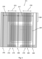
- Fig. 3 discloses a top view 201 of an ESD protection semiconductor device in accordance with the present disclosure
- Fig. 4 discloses an exploded view 211 of an ESD protection semiconductor device in accordance with the present disclosure.
- the width of the ESD semiconductor device is indicated with reference numeral 205. As shown, the ESD semiconductor device is in the shape of an endless loop.
- the ESD semiconductor device encompasses a semiconductor material that is indicated with reference numeral 203.
- This material may form, for example, the gate pad of a corresponding Metal Oxide Semiconductor, MOS, Field Effect Transistor, FET, MOSFET.
- the area at the outside of the ESD semiconductor device is indicated with reference numeral 204.
- This material may be connected to, for example, the source pad of the MOSFET.
- the ESD semiconductor device thus connects the gate pad at one side to the source pad at the other side of the device.
- the four diodes of the ESD semiconductor device are located between those two pads, along a circle.
- the ESD protection semiconductor device comprises two ESD regions, wherein each ESD region is construed such that it consists of two back to back diodes. These two ESD regions are connected to one another via the floating terminal. More specifically, one end of a second diode of the first ESD region is connected to one end of a first diode in the second ESD region.
- the floating terminal assures that such an electrical connection is actually made.
- the floating terminal comprises multiple individual floating strips provided electrically isolated from each other and each for providing an individual connections between said second diode region and said third diode region.
- the exploded view 202 is shown in figure 4 .
- the first back-to-back diode is indicated with reference numeral 216.
- the second back-to-back diode is indicated with reference numeral 217.
- the ESD protection semiconductor device comprises three isolating trenches as indicated with reference numerals 212, 222 and 223. These trenches comprise isolating material, like oxide or the like, for assuring a robust isolation between the ESD protection semiconductor device and the semiconductor device that it actually intends to protect.
- the first ESD region is indicated with reference numeral 213, and the first diode region is indicated with reference numeral 214 and the second diode region is indicated with reference numeral 215.
- the second ESD region is indicated with reference numeral 218, the third diode region is indicated with reference numeral 219 and the fourth diode region is indicated with reference numeral 220.
- the floating terminal is indicated with reference numeral 221.
- One of the aspects of the present disclosure is that the connection to the first ESD terminal and the second ESD terminal, for example the connections towards the gate and source pad of a MOSFET, are made in between the different floating terminals. This is visually indicated with reference numeral 224.
Landscapes
- Semiconductor Integrated Circuits (AREA)
- Metal-Oxide And Bipolar Metal-Oxide Semiconductor Integrated Circuits (AREA)
Abstract
Description
- The present disclosure relates to the field of Electrostatic Discharge, ESD, protection and, more in particular, to an ESD protection semiconductor device implemented in a semiconductor material.
- A Trench Gate Metal Oxide Semiconductor, MOS, Field Effect Transistor, FET, typically comprises a source region towards a first major surface of the MOSFET and a drain region formed on a second major surface, opposite to the first major surface. The source and drain region have the same conductivity type.
- A channel-accommodating region, i.e. a body region, is provided between the source and drain region, which channel-accommodating region is of a different conductivity type to that of the source and drain region. A conductive channel is to be construed between the source region and the drain region to assure that the MOSFET is turned on. To facilitate the creation of such a channel, a trench gate electrode is provided close to, but not in electrical contact with, the channel-accommodating region.
- Typical for the trench gate MOSFET is that the current is conducted vertically from one surface to the other so as to achieve a high drive capability. It may be realized by packing trenches on a chip, deep enough to cross the oppositely doped body region, i.e. channel-accommodating region, below the top surface.
- The gate trench is typically provided with some sort of oxide, to assure that the gate electrode is electrically isolated from the channel-accommodating region. Providing a voltage bias at the gate trench will then produce an electrical field which extends into, and thus also locally depletes and/or inverts, the channel-accommodating region.
- Trench gate MOSFETs are able to cope with high voltage operations, for example in the region of 100V or above. In addition, such MOSFETs may be able to cope with high reverse bias voltages between the source region and the drain region, without that the MOSFET will break down of pass any significant reverse current.
- The above is typically achieved by introducing a drift region between the drain region and the channel-accommodating region, wherein the drift region has the same conductivity type as the source region and the drain region. The drift region, however, typically has a lower doping concentration. The drain region forms a PN junction at the interface with the channel-accommodating region which serves to block the reverse bias current.
- For N-channel MOSFETs, the drain region is positive relative to the source region. If the source region is positive relative to the drain region, then the body-drain junction may become biased and current may be conducted via the drain region and the source region. Alternatively, for P-channel MOSFETs, the drain region is negative relative to the source region. If the source region is negative relative to the drain region, then the body-drain junction may again conduct current. The breakdown voltage is dependent on the thickness of the drift region wherein the greater the thickness, the higher the breakdown voltage.
- When comparing the more conventional lateral MOSFETs with vertical trench-gate MOSFETs, like the one described above, it is clear that in vertical trench-gate MOSFETs, the channel regions are designed along the vertical walls of the trenches, rather than laterally. This allows for a high density of channels, i.e. two for each trench, per unit area of the device.
- One of the downsides of MOSFETs is that they may be prone Electrostatic Discharge, ESD. The same is applicable for other type of semiconductor devices.
- A summary of aspects of certain examples disclosed herein is set forth below. It should be understood that these aspects are presented merely to provide the reader with a brief summary of these certain embodiments and that these aspects are not intended to limit the scope of this disclosure. Indeed, this disclosure may encompass a variety of aspects and/or a combination of aspects that may not be set forth.
- It is an object of the present disclosure to provide for an Electrostatic Discharge, ESD, protection semiconductor device for providing ESD protection between a first and a second terminal of another semiconductor device.
- It is a further object of the present disclosure to provide for a Metal Oxide Semiconductor, MOS, Field Effect Transistor, FET, MOSFET, wherein the MOSFET further comprises an ESD protection semiconductor device in accordance with the present disclosure.
- In a first aspect, there is provided An Electrostatic Discharge, ESD, protection semiconductor device for providing ESD protection between a first and a second terminal of another semiconductor device, the ESD protection device comprising a semiconductor body having a first major surface, wherein the semiconductor device further comprises a first ESD terminal arranged to be connected to a first terminal of the other semiconductor device, a second ESD terminal arranged to be connected to a second terminal of the other semiconductor device, and a floating terminal, and wherein the semiconductor body further comprises:
- a first ESD region of a first conductivity type and extending from the first major surface into said semiconductor body, wherein the first ESD region comprises:
- a first diode region of a second conductivity type, wherein the first diode region is connected to the first ESD terminal;
- a second diode region of the second conductivity type, spaced apart from said first diode region, wherein the second diode region is connected to the floating terminal;
- a second ESD region of a first conductivity type and extending from the first major surface into said semiconductor body, wherein the second ESD region comprises:
- a third diode region of the second conductivity type, wherein the third diode region is connected to the floating terminal;
- a fourth diode region of the second conductivity type, spaced apart from said third diode region, wherein the fourth diode region is connected to the second ESD terminal,
- said floating terminal comprises multiple individual floating strips provided electrically isolated from each other and each for providing an individual connections between said second diode region and said third diode region.
- The present disclosure has several advantages over more traditional ESD protection.
- First of all, the inventors have found that it may be beneficial to incorporate ESD protection in the semiconductor body. That is, the diodes are actually implemented in the semiconductor body, for example in silicon material. This may ensure that the leakage current is relatively low, for example a couple of nano Ampere.
- Second, another advantage is that in a top view of said ESD protection semiconductor device, said ESD protection semiconductor device is elongated, and wherein said floating terminal comprises individual, electrically isolated, floating strips for providing connections between said second diode region and said third diode region.
- The main advantage of this aspect is that the active area of the semiconductor material is improved. The span of the diodes may be reduced, for example to about 14,5 µm, as will be apparent later when referring to the figures.
- The introduction of the new design for the floating terminal fulfils different design rules that need to be considered when designing ESD protection. The present disclosure discloses creating individual, electrically, isolated floating strips. This means that those strips will not "cover" the entire span of the elongated ESD protection semiconductor device.
- The space in between subsequent floating strips may be utilized for connection to the first and/or second terminal of the another semiconductor device. This is beneficial for reducing the size of the ESD protection semiconductor device, and thus for improving the active area.
- The above described ESD semiconductor device effectively establishes the introduction of four back to back diodes between the first terminal and the second terminal of the another semiconductor device, as there are four interfaces or boundaries between two semiconductor material types. The diodes are oriented in that the cathodes of the diodes are connected to each other. This is accomplished by the layout of the ESD region and the specific diode regions inside that corresponding ESD region.
- Typically, the first conductivity type is N-type, and wherein the second conductivity type is P-type, or vice-versa.
- It is noted that the ESD protection device may be especially useful for protecting a 12Volt gate to source voltage of a MOSFET. In case higher voltages are to be protected, even more diodes may be utilized in the design. So, six, eight, or even ten diodes may be used instead of the four diodes. The present disclosure is thus not limited to four diodes, but to at least four diodes.
- In an example, the ESD protection device comprises a first, a second and a third isolating trench, wherein each of said three trenches extend into the semiconductor body from the major surface, and wherein said first ESD region is oriented between said first and second isolating trench and wherein said second ESD region is oriented between said second and third isolating trench.
- The inventors have found that it might be beneficial to introduce isolating trenches to ensure that the functioning of the ESD protection semiconductor device does not influence the functioning of the another semiconductor device.
- Another option is to introduce isolating regions, for example by sacrificing area of the semiconductor material or by a different form of isolation material or design or the like.
- The isolating trenches may, for example, be provided with oxide material or any other type of isolating material.
- In a further example, in said top view of said ESD protection semiconductor device, a shape of said ESD semiconductor device is a geometric shape thereby enclosing a semiconductor material of said semiconductor body.
- For example, the enclosed semiconductor material is to be connected to said first terminal of said another semiconductor device.
- The above described example provides for a relatively robust ESD protection for the another semiconductor device. The another semiconductor device may be manufactured in such a way that its first terminal is aligned with the enclosed semiconductor material of the ESD semiconductor device. This allows for an effective ESD protection.
- In a further example, the first, second, third and fourth diode regions are each endless loops, seen in said top view, surrounding a central region of semiconductor material forming the first ESD terminal.
- The above may entail that there is no end face of the ESD protection semiconductor device, but that the ESD protection semiconductor device is construed in such a way that there is effectively no beginning or end, just like a circle.
- In an example, in said top view of said ESD protection semiconductor device:
- said first diode region is connected to the first ESD terminal at locations in between said individual, electrically isolated, floating strips, and/or
- said fourth diode region is connected to the second ESD terminal at said locations in between said individual, electrically isolated, floating strips.
- The above described example provides for an effective way of protecting a MOSFET, wherein the first terminal is the gate terminal of the MOSFET and the second terminal if the source terminal of the MOSFET.
- In a second aspect of the present disclosure, there is provided a Metal Oxide Semiconductor, MOS, Field Effect Transistor, FET, MOSFET, having a gate pad and a source pad embodied in a semiconductor material, wherein said MOSFET further comprises an Electrostatic Discharge, ESD, protection semiconductor device in accordance with any of the previous examples.
- It is noted that the advantages as explained with reference to the first aspect of the present disclosure, being the ESD protection semiconductor device, are also applicable to the second aspect of the present disclosure, being the MOSFET.
- In a specific example, the ESD protection device is aligned with said gate pad of said MOSFET.
- In a third aspect of the present disclosure, there is provided a method of manufacturing an Electrostatic Discharge, ESD, protection device in accordance with any of the examples provided above, wherein said method comprises the steps of:
- forming a first ESD region of a first conductivity type and extending from the first major surface into said semiconductor body;
- forming a first diode region of the second conductivity type, in the first ESD region, wherein the first diode region is connected to the first ESD terminal;
- forming a second diode region of the second conductivity type, in the first ESD region, spaced apart from said first diode region, wherein the second diode region is connected to a floating terminal;
- forming a second ESD region of a first conductivity type and extending from the first major surface into said semiconductor body:
- a third diode region of the second conductivity type, in the second ESD region, wherein the third diode region is connected to the floating terminal;
- a fourth diode region of the second conductivity type, in the second ESD region, spaced apart from said third diode region, wherein the fourth diode region is connected to the second ESD terminal,
- forming said floating terminal comprising forming individual, electrically isolated, floating strips for providing connections between said second diode region and said third diode region.
- In an example, the method further comprises the step of:
- forming a first, a second and a third isolating trench, wherein each of said three trenches extend into the semiconductor body from the major surface, and wherein said first ESD region is oriented between said first and second isolating trench and wherein said second ESD region is oriented between said second and third isolating trench.
- In a further example, the ESD protection semiconductor device is formed such that in said top view of said ESD protection semiconductor device, a shape of said ESD protection semiconductor device is a geometric shape thereby enclosing a semiconductor material of said semiconductor body.
- In another example, the ESD protection semiconductor device is formed such that the first, second, third and fourth diode regions are each endless loops, seen in said top view, surrounding a central region of semiconductor material forming the first ESD terminal.
- In yet another example, the ESD protection semiconductor device is formed such that, in said top view of said ESD protection semiconductor device:
- said first diode region is connected to the first ESD terminal at locations in between said individual, electrically isolated, floating strips, and/or
- said fourth diode region is connected to the second ESD terminal at said locations in between said individual, electrically isolated, floating strips.
- The present disclosure is described in conjunction with the appended figures. It is emphasized that, in accordance with the standard practice in the industry, various features are not drawn to scale. In fact, the dimensions of the various features may be arbitrarily increased or reduced for clarity of discussion.
- In the appended figures, similar components and/or features may have the same reference label. Further, various components of the same type may be distinguished by following the reference label by a dash and a second label that distinguishes among the similar components. If only the first reference label is used in the specification, the description is applicable to any one of the similar components having the same first reference label irrespective of the second reference label.
- The above and other aspects of the disclosure will be apparent from and elucidated with reference to the examples described hereinafter.
-
-
Fig. 1 discloses Electro Static Discharge, ESD, protection for a Metal oxide Semiconductor, MOS, Field Effect Transistor, FET; -
Fig. 2 discloses a schematic overview as well as a realistic implementation of a MOSFET in accordance with the present disclosure; -
Fig. 3 discloses a top view of an ESD protection semiconductor device in accordance with the present disclosure; -
Fig. 4 discloses an exploded view of an ESD protection semiconductor device in accordance with the present disclosure. - It is noted that in the description of the figures, same reference numerals refer to the same or similar components performing a same or essentially similar function.
- A more detailed description is made with reference to particular examples, some of which are illustrated in the appended drawings, such that the manner in which the features of the present disclosure may be understood in more detail. It is noted that the drawings only illustrate typical examples and are therefore not to be considered to limit the scope of the subject matter of the claims. The drawings are incorporated for facilitating an understanding of the disclosure and are thus not necessarily drawn to scale. Advantages of the subject matter as claimed will become apparent to those skilled in the art upon reading the description in conjunction with the accompanying drawings.
- The ensuing description above provides preferred exemplary embodiment(s) only, and is not intended to limit the scope, applicability or configuration of the disclosure. Rather, the ensuing description of the preferred exemplary embodiment(s) will provide those skilled in the art with an enabling description for implementing a preferred exemplary embodiment of the disclosure, it being understood that various changes may be made in the function and arrangement of elements, including combinations of features from different embodiments, without departing from the scope of the disclosure.
- Unless the context clearly requires otherwise, throughout the description and the claims, the words "comprise," "comprising," and the like are to be construed in an inclusive sense, as opposed to an exclusive or exhaustive sense; that is to say, in the sense of "including, but not limited to." As used herein, the terms "connected," "coupled," or any variant thereof means any connection or coupling, either direct or indirect, between two or more elements; the coupling or connection between the elements can be physical, logical, electromagnetic, or a combination thereof. Additionally, the words "herein," "above," "below," and words of similar import, when used in this application, refer to this application as a whole and not to any particular portions of this application. Where the context permits, words in the Detailed Description using the singular or plural number may also include the plural or singular number respectively. The word "or," in reference to a list of two or more items, covers all of the following interpretations of the word: any of the items in the list, all of the items in the list, and any combination of the items in the list.
- These and other changes can be made to the technology in light of the following detailed description. While the description describes certain examples of the technology, and describes the best mode contemplated, no matter how detailed the description appears, the technology can be practiced in many ways. Details of the system may vary considerably in its specific implementation, while still being encompassed by the technology disclosed herein. As noted above, particular terminology used when describing certain features or aspects of the technology should not be taken to imply that the terminology is being redefined herein to be restricted to any specific characteristics, features, or aspects of the technology with which that terminology is associated. In general, the terms used in the following claims should not be construed to limit the technology to the specific examples disclosed in the specification, unless the Detailed Description section explicitly defines such terms. Accordingly, the actual scope of the technology encompasses not only the disclosed examples, but also all equivalent ways of practicing or implementing the technology under the claims.
-
Figure 1 discloses Electro Static Discharge, ESD, protection for a Metal oxide Semiconductor, MOS, Field Effect Transistor,FET 1 having asource 4, adrain 2 and agate 3 terminal. - In MOSFETs, there are typically three basic ESD induced failures namely junction damage, gate oxide damage and metallization burnout. These failures are usually thermally induced, indicating that damage occurs once the temperature of the local area exceeds a critical value, often the melting point of the material.
- Junction damage may be caused by the injection of an ESD transient of sufficient energy and duration to force the junction into secondary breakdown. Junction damage is often characterized by high reverse bias leakage current or a total short.
- The so-called gate oxide damage may occur when the
gate 3 is subjected to an ESD pulse of high enough magnitude to cause the gate oxide to breakdown. For MOSFETs, the gate oxide is typically very thin resulting in varying degrees of ESD sensitivity. - Metallization burnout may exist in metal interconnects or contacts. It may occur if any current flowing through the metal forces a temperature rise that is high enough to reach the melting point of the material. Metallization burnout is often a secondary effect, occurring after the initial junction or gate oxide failure.
- To protect a MOSFET from ESD, the main objective is typically to clamp the
gate 3 tosource 4 voltage from reaching the destructive voltage. A typicalESD protection device 5 clamps the voltage to a lower value at the occurrence of the ESD strike to minimize the voltage seen at the gate of MOSFET. The protection device may shunt current to ground and away from the protectedgate 3. - During this period, the clamping voltage and residual current seen at the
gate 3 may depend upon the breakdown voltage and the dynamic resistance of the protection device. Once the ESD strike is fully dissipated, theESD protection device 5 attempts to return to a high impedance state. There are several types ofESD protection devices 5 available today, but most commonly used are Transient-voltage-suppression, TVS, and Zener diodes. Infigure 1 , four cascadeddiodes 5 are shown that operate as ESD protection for the MOSFET. - One of the downsides of using such a topology as shown in
figure 1 is that the leakage current fromgate 3 tosource 4 is relatively high. - The present disclosure is directed to an independent ESD protection semiconductor device. Independent in the sense that it may be used for protecting an MOSFET, but it may also be used for protecting any other type of semiconductor device. Further, the ESD protection semiconductor device is implemented in the semiconductor body, i.e. in the silicon material of the semiconductor body.
- An example of the ESD
protection semiconductor device 101 is shown infigure 2 . - At the right hand side of
figure 2 a schematic overview is provided of an ESD protection semiconductor device in accordance with the present disclosure and at the left hand side an actual manufactured example is provided. - The ESD
protection semiconductor device 101 shown infigure 2 comprises a semiconductor body having a firstmajor surface 112, and threetrenches 105 extending from the firstmajor surface 112 into the semiconductor body. Thetrenches 105 are isolating trenches, i.e. the comprise an isolating material like oxide or the like. - A
substrate 103 is provided that may form the drain region of the MOSFET, in case a particular MOSFET is to be protected for ESD. It is noted that the substrate may be split into a drain region and a drift region but is not further elucidated in more detail with respect tofigure 2 . - A
further region 113 is provided, wherein thefurther region 113 is abut thetrenches 105. - The ESD
protection semiconductor device 101 is construed such that it may be connected between the gate and the source terminal of a MOSFET, for example. The connection to the gate may be realized using the terminal indicated withreference numeral 104. The connection to the source may be realized using the terminal indicated withreference numeral 102. - A first ESD region of a first conductivity type is provided as indicated with
reference numeral 106 and extends from the firstmajor surface 112 into said semiconductor body, wherein thefirst ESD region 106 comprises: - a
first diode region 107 of the second conductivity type, wherein thefirst diode region 107 is connected to thefirst ESD terminal 104; - a
second diode region 108 of the second conductivity type, spaced apart from saidfirst diode region 107, wherein thesecond diode region 108 is connected to a floatingterminal 115; - a
second ESD region 110 of a first conductivity type and extending from the firstmajor surface 112 into said semiconductor body, wherein thesecond ESD region 110 comprises:- a
third diode region 109 of the second conductivity type, wherein thethird diode region 109 is connected to the floating terminal; - a
fourth diode region 111 of the second conductivity type, spaced apart from saidthird diode region 109, wherein thefourth diode region 111 is connected to thesecond ESD terminal 102,
- a
- the floating
terminal 115 comprises individual, electrically isolated, floating strips for providing connections between said second diode region and said third diode region. - It is noted that the connection as indicated with
reference numeral 114 may be implemented for providing more robustness to the ESDprotection semiconductor device 101. - The specific layout of the floating
terminal 115 is discussed with respect tofigures 3 and4 . -
Fig. 3 discloses atop view 201 of an ESD protection semiconductor device in accordance with the present disclosure andFig. 4 discloses an explodedview 211 of an ESD protection semiconductor device in accordance with the present disclosure. - The exploded view is indicated with
reference numeral 202. Both figures will be explained simultaneously here below for improving the understanding of the present disclosure. - The width of the ESD semiconductor device is indicated with
reference numeral 205. As shown, the ESD semiconductor device is in the shape of an endless loop. - The ESD semiconductor device encompasses a semiconductor material that is indicated with
reference numeral 203. This material may form, for example, the gate pad of a corresponding Metal Oxide Semiconductor, MOS, Field Effect Transistor, FET, MOSFET. - The area at the outside of the ESD semiconductor device is indicated with
reference numeral 204. This material may be connected to, for example, the source pad of the MOSFET. - The ESD semiconductor device thus connects the gate pad at one side to the source pad at the other side of the device. The four diodes of the ESD semiconductor device are located between those two pads, along a circle.
- The ESD protection semiconductor device comprises two ESD regions, wherein each ESD region is construed such that it consists of two back to back diodes. These two ESD regions are connected to one another via the floating terminal. More specifically, one end of a second diode of the first ESD region is connected to one end of a first diode in the second ESD region.
- The floating terminal assures that such an electrical connection is actually made.
- In accordance with the present disclosure, the floating terminal comprises multiple individual floating strips provided electrically isolated from each other and each for providing an individual connections between said second diode region and said third diode region.
- As shown in
figure 3 , in total eighteen (18) individual floating strips are provided for providing the electrical connection throughout the elongated ESD regions. One of the benefits is that the width of the diodes may be made smaller, as will be apparent later here below. - The exploded
view 202 is shown infigure 4 . The first back-to-back diode is indicated withreference numeral 216. The second back-to-back diode is indicated withreference numeral 217. - The ESD protection semiconductor device comprises three isolating trenches as indicated with
reference numerals - The first ESD region is indicated with
reference numeral 213, and the first diode region is indicated withreference numeral 214 and the second diode region is indicated withreference numeral 215. The second ESD region is indicated withreference numeral 218, the third diode region is indicated withreference numeral 219 and the fourth diode region is indicated withreference numeral 220. - The floating terminal is indicated with
reference numeral 221. One of the aspects of the present disclosure, is that the connection to the first ESD terminal and the second ESD terminal, for example the connections towards the gate and source pad of a MOSFET, are made in between the different floating terminals. This is visually indicated withreference numeral 224. - To reduce the number of claims, certain aspects of the technology are presented below in certain claim forms, but the applicant contemplates the various aspects of the technology in any number of claim forms. For example, while some aspect of the technology may be recited as a computer-readable medium claim, other aspects may likewise be embodied as a computer-readable medium claim, or in other forms, such as being embodied in a means-plus-function claim.
In the description above, for the purposes of explanation, numerous specific details are set forth in order to provide a thorough understanding of implementations of the disclosed technology. It will be apparent, however, to one skilled in the art that embodiments of the disclosed technology may be practiced without some of these specific details. - Other variations to the disclosed embodiments can be understood and effected by those skilled in the art in practicing the claimed invention, from a study of the drawings, the disclosure and the appended claims. In the claims, the word "comprising" does not exclude other elements or steps, and the indefinite article "a" or "an" does not exclude a plurality. The mere fact that certain measures are recited in mutually different dependent claims does not indicate that a combination of these measures cannot be used to advantage. Any reference signs in the claims should not be construed as limiting the scope thereof.
Claims (13)
- An Electrostatic Discharge, ESD, protection semiconductor device for providing ESD protection between a first and a second terminal of another semiconductor device, the ESD protection device comprising a semiconductor body having a first major surface, wherein the semiconductor device further comprises a first ESD terminal arranged to be connected to a first terminal of the other semiconductor device, a second ESD terminal arranged to be connected to a second terminal of the other semiconductor device, and a floating terminal, and wherein the semiconductor body further comprises:- a first ESD region of a first conductivity type and extending from the first major surface into said semiconductor body, wherein the first ESD region comprises:- a first diode region of a second conductivity type, wherein the first diode region is connected to the first ESD terminal;- a second diode region of the second conductivity type, spaced apart from said first diode region, wherein the second diode region is connected to the floating terminal;- a second ESD region of a first conductivity type and extending from the first major surface into said semiconductor body, wherein the second ESD region comprises:wherein, seen in a view of said ESD protection semiconductor device perpendicular to said first major surface, said first and second ESD regions are both elongated, and wherein- a third diode region of the second conductivity type, wherein the third diode region is connected to the floating terminal;- a fourth diode region of the second conductivity type, spaced apart from said third diode region, wherein the fourth diode region is connected to the second ESD terminal,- said floating terminal comprises multiple individual floating strips provided electrically isolated from each other and each for providing an individual connections between said second diode region and said third diode region.
- An ESD protection device in accordance with claim 1, wherein said ESD protection device comprises a first, a second and a third isolating trench, wherein each of said three trenches extends into the semiconductor body from the major surface, and wherein said first ESD region is oriented between said first and second isolating trench and wherein said second ESD region is oriented between said second and third isolating trench.
- An ESD protection device in accordance with any of the previous claims, wherein, in said top view of said ESD protection semiconductor device, a shape of said ESD semiconductor device is a geometric shape thereby enclosing a semiconductor material of said semiconductor body.
- An ESD protection device in accordance with claim 3, wherein said enclosed semiconductor material is to be connected to said first terminal of said other semiconductor device.
- An ESD protection device in accordance with any of the claims 3 - 4, wherein the first and second ESD regions are each endless loops, seen in said top view, thereby enclosing said semiconductor material of said semiconductor body.
- An ESD protection device in accordance with any of the previous claims, wherein, seen in said view of said ESD protection semiconductor device perpendicular to said first major surface:- said first diode region is connected to the first ESD terminal at locations in between said multiple individual floating strips, and/or- said fourth diode region is connected to the second ESD terminal at said locations in between said multiple individual floating strips.
- A Metal Oxide Semiconductor, MOS, Field Effect Transistor, FET, MOSFET, having a gate pad and a source pad embodied in a semiconductor material, wherein said MOSFET further comprises an Electrostatic Discharge, ESD, protection semiconductor device in accordance with any of the previous claims.
- A MOSFET in accordance with claim 7, wherein said ESD protection device is aligned with said gate pad of said MOSFET such that said first ESD terminal is connected to said gate pad.
- A method of manufacturing an Electrostatic Discharge, ESD, protection device in accordance with any of the claims 1 - 6, wherein said method comprises the steps of:- forming a first ESD region of a first conductivity type and extending from the first major surface into said semiconductor body;- forming a first diode region of the second conductivity type, in the first ESD region;- forming a second diode region of the second conductivity type, in the first ESD region, spaced apart from said first diode region;- forming a second ESD region of a first conductivity type and extending from the first major surface into said semiconductor body:wherein, in a top view of said ESD protection semiconductor device, said first and second ESD regions are both elongated, and wherein said method comprises the step of:- forming a third diode region of the second conductivity type, in the second ESD region;- forming a fourth diode region of the second conductivity type, in the second ESD region, spaced apart from said third diode region,- forming said floating terminal comprising forming multiple individual floating strips provided electrically isolated from each other and each for providing an individual connections between said second diode region and said third diode region.
- A method in accordance with claim 9, wherein said method further comprises the step of:- forming a first, a second and a third isolating trench, wherein each of said three trenches extends into the semiconductor body from the major surface, and wherein said first ESD region is oriented between said first and second isolating trench and wherein said second ESD region is oriented between said second and third isolating trench.
- A method in accordance with any of the claims 9 - 10, wherein, said ESD protection semiconductor device is formed such that in said top view of said ESD protection semiconductor device, a shape of said ESD protection semiconductor device is a geometric shape thereby enclosing a semiconductor material of said semiconductor body.
- A method in accordance with claim 12, wherein the first and second ESD regions are each endless loops, seen in said top view, thereby enclosing said semiconductor material of said semiconductor body.
- A method in accordance with any of the claims 9 - 12, wherein said ESD protection semiconductor device is formed such that, wherein, seen in said view of said ESD protection semiconductor device perpendicular to said first major surface:- said first diode region is connected to the first ESD terminal at locations in between said multiple individual floating strips, and/or- said fourth diode region is connected to the second ESD terminal at said locations in between said multiple individual floating strips.
Priority Applications (3)
| Application Number | Priority Date | Filing Date | Title |
|---|---|---|---|
| EP22200290.9A EP4350769B1 (en) | 2022-10-07 | 2022-10-07 | An electrostatic discharge, esd, protection semiconductor device for providing esd protection between a first and a second terminal of another semiconductor device, as well as a corresponding metal oxide semiconductor, mos, field effect transistor, fet, and a related method |
| CN202311283117.0A CN117855211A (en) | 2022-10-07 | 2023-10-07 | ESD protection semiconductor device and manufacturing method thereof |
| US18/483,047 US12610623B2 (en) | 2022-10-07 | 2023-10-09 | Electrostatic discharge, ESD, protection semiconductor device for providing ESD protection between a first and a second terminal of another semiconductor device, as well as a corresponding metal oxide semiconductor, MOS, field effect transistor, FET, and a related method |
Applications Claiming Priority (1)
| Application Number | Priority Date | Filing Date | Title |
|---|---|---|---|
| EP22200290.9A EP4350769B1 (en) | 2022-10-07 | 2022-10-07 | An electrostatic discharge, esd, protection semiconductor device for providing esd protection between a first and a second terminal of another semiconductor device, as well as a corresponding metal oxide semiconductor, mos, field effect transistor, fet, and a related method |
Publications (2)
| Publication Number | Publication Date |
|---|---|
| EP4350769A1 true EP4350769A1 (en) | 2024-04-10 |
| EP4350769B1 EP4350769B1 (en) | 2025-07-09 |
Family
ID=83689310
Family Applications (1)
| Application Number | Title | Priority Date | Filing Date |
|---|---|---|---|
| EP22200290.9A Active EP4350769B1 (en) | 2022-10-07 | 2022-10-07 | An electrostatic discharge, esd, protection semiconductor device for providing esd protection between a first and a second terminal of another semiconductor device, as well as a corresponding metal oxide semiconductor, mos, field effect transistor, fet, and a related method |
Country Status (3)
| Country | Link |
|---|---|
| US (1) | US12610623B2 (en) |
| EP (1) | EP4350769B1 (en) |
| CN (1) | CN117855211A (en) |
Citations (4)
| Publication number | Priority date | Publication date | Assignee | Title |
|---|---|---|---|---|
| JP2007035796A (en) * | 2005-07-25 | 2007-02-08 | Matsushita Electric Ind Co Ltd | Semiconductor device |
| US20110210418A1 (en) * | 2010-03-01 | 2011-09-01 | Kai Esmark | Electrostatic Discharge Devices |
| US20130075809A1 (en) * | 2011-09-27 | 2013-03-28 | Force Mos Technology Co. Ltd. | Semiconductor power device with embedded diodes and resistors using reduced mask processes |
| US20220102549A1 (en) * | 2020-09-30 | 2022-03-31 | Infineon Technologies Ag | Silicon carbide device with transistor cell and clamp region |
Family Cites Families (3)
| Publication number | Priority date | Publication date | Assignee | Title |
|---|---|---|---|---|
| US12444934B2 (en) * | 2020-03-31 | 2025-10-14 | Taiwan Semiconductor Manufacturing Company, Ltd. | Electrostatic discharge (ESD) protection circuit and method of operating the same |
| US11626719B2 (en) * | 2020-03-31 | 2023-04-11 | Taiwan Semiconductor Manufacturing Company, Ltd. | Electrostatic discharge (ESD) protection circuit and method of operating the same |
| US11532610B2 (en) * | 2020-06-24 | 2022-12-20 | Amazing Microelectronic Corp. | Electrostatic discharge protection structure and electrostatic discharge protection circuit with low parasitic capacitance thereof |
-
2022
- 2022-10-07 EP EP22200290.9A patent/EP4350769B1/en active Active
-
2023
- 2023-10-07 CN CN202311283117.0A patent/CN117855211A/en active Pending
- 2023-10-09 US US18/483,047 patent/US12610623B2/en active Active
Patent Citations (4)
| Publication number | Priority date | Publication date | Assignee | Title |
|---|---|---|---|---|
| JP2007035796A (en) * | 2005-07-25 | 2007-02-08 | Matsushita Electric Ind Co Ltd | Semiconductor device |
| US20110210418A1 (en) * | 2010-03-01 | 2011-09-01 | Kai Esmark | Electrostatic Discharge Devices |
| US20130075809A1 (en) * | 2011-09-27 | 2013-03-28 | Force Mos Technology Co. Ltd. | Semiconductor power device with embedded diodes and resistors using reduced mask processes |
| US20220102549A1 (en) * | 2020-09-30 | 2022-03-31 | Infineon Technologies Ag | Silicon carbide device with transistor cell and clamp region |
Also Published As
| Publication number | Publication date |
|---|---|
| US20240120331A1 (en) | 2024-04-11 |
| CN117855211A (en) | 2024-04-09 |
| EP4350769B1 (en) | 2025-07-09 |
| US12610623B2 (en) | 2026-04-21 |
Similar Documents
| Publication | Publication Date | Title |
|---|---|---|
| US7511357B2 (en) | Trenched MOSFETs with improved gate-drain (GD) clamp diodes | |
| EP0485174B1 (en) | Power mosfet transistor circuit with active clamp | |
| KR101617958B1 (en) | Vertical nanowire transistor for input/output structure | |
| US8044457B2 (en) | Transient over-voltage clamp | |
| US6229180B1 (en) | MOS type semiconductor apparatus | |
| US9431389B2 (en) | ESD transistor for high voltage and ESD protection circuit thereof | |
| US5291051A (en) | ESD protection for inputs requiring operation beyond supply voltages | |
| KR100276414B1 (en) | Insulated gate type semiconductor device | |
| EP1808900A2 (en) | Multiple phase motor driver with bidirectional blocking accumulation-mode trench power mosfets | |
| US5844280A (en) | Device for protecting a semiconductor circuit | |
| JP2006517350A (en) | Low voltage NMOS type electrostatic discharge clamp | |
| US9711643B2 (en) | ESD robust MOS device | |
| JPH11251594A (en) | Power MOSFET with voltage clamped gate | |
| CN101019319A (en) | A semiconductor switch arrangement and an electronic device | |
| EP0218685B1 (en) | Electrostatic discharge input protection network | |
| KR100510096B1 (en) | Trench-gated power mosfet | |
| EP0967659A1 (en) | IGBT Power device with improved resistance to reverse power pulses | |
| US12550456B2 (en) | Trench gate metal oxide semiconductor field effect transistor and method of manufacture | |
| EP4350769B1 (en) | An electrostatic discharge, esd, protection semiconductor device for providing esd protection between a first and a second terminal of another semiconductor device, as well as a corresponding metal oxide semiconductor, mos, field effect transistor, fet, and a related method | |
| US12237412B2 (en) | Protection structures for semiconductor devices with sensor arrangements | |
| KR100504203B1 (en) | Protecting device of semiconductor device | |
| JP4696356B2 (en) | Semiconductor device | |
| KR20070092637A (en) | Semiconductor devices | |
| US5521413A (en) | Semiconductor device having a solid metal wiring with a contact portion for improved protection | |
| KR101986711B1 (en) | ESD protected power semiconductor device |
Legal Events
| Date | Code | Title | Description |
|---|---|---|---|
| PUAI | Public reference made under article 153(3) epc to a published international application that has entered the european phase |
Free format text: ORIGINAL CODE: 0009012 |
|
| STAA | Information on the status of an ep patent application or granted ep patent |
Free format text: STATUS: THE APPLICATION HAS BEEN PUBLISHED |
|
| AK | Designated contracting states |
Kind code of ref document: A1 Designated state(s): AL AT BE BG CH CY CZ DE DK EE ES FI FR GB GR HR HU IE IS IT LI LT LU LV MC ME MK MT NL NO PL PT RO RS SE SI SK SM TR |
|
| STAA | Information on the status of an ep patent application or granted ep patent |
Free format text: STATUS: REQUEST FOR EXAMINATION WAS MADE |
|
| 17P | Request for examination filed |
Effective date: 20241008 |
|
| RBV | Designated contracting states (corrected) |
Designated state(s): AL AT BE BG CH CY CZ DE DK EE ES FI FR GB GR HR HU IE IS IT LI LT LU LV MC ME MK MT NL NO PL PT RO RS SE SI SK SM TR |
|
| REG | Reference to a national code |
Ref country code: DE Ref legal event code: R079 Free format text: PREVIOUS MAIN CLASS: H01L0027020000 Ipc: H10D0030660000 Ref country code: DE Ref legal event code: R079 Ref document number: 602022017241 Country of ref document: DE Free format text: PREVIOUS MAIN CLASS: H01L0027020000 Ipc: H10D0030660000 |
|
| GRAP | Despatch of communication of intention to grant a patent |
Free format text: ORIGINAL CODE: EPIDOSNIGR1 |
|
| STAA | Information on the status of an ep patent application or granted ep patent |
Free format text: STATUS: GRANT OF PATENT IS INTENDED |
|
| RIC1 | Information provided on ipc code assigned before grant |
Ipc: H10D 89/60 20250101ALI20250124BHEP Ipc: H10D 84/00 20250101ALI20250124BHEP Ipc: H10D 30/66 20250101AFI20250124BHEP |
|
| INTG | Intention to grant announced |
Effective date: 20250210 |
|
| GRAS | Grant fee paid |
Free format text: ORIGINAL CODE: EPIDOSNIGR3 |
|
| GRAA | (expected) grant |
Free format text: ORIGINAL CODE: 0009210 |
|
| STAA | Information on the status of an ep patent application or granted ep patent |
Free format text: STATUS: THE PATENT HAS BEEN GRANTED |
|
| AK | Designated contracting states |
Kind code of ref document: B1 Designated state(s): AL AT BE BG CH CY CZ DE DK EE ES FI FR GB GR HR HU IE IS IT LI LT LU LV MC ME MK MT NL NO PL PT RO RS SE SI SK SM TR |
|
| REG | Reference to a national code |
Ref country code: GB Ref legal event code: FG4D |
|
| REG | Reference to a national code |
Ref country code: CH Ref legal event code: EP |
|
| REG | Reference to a national code |
Ref country code: IE Ref legal event code: FG4D |
|
| REG | Reference to a national code |
Ref country code: DE Ref legal event code: R096 Ref document number: 602022017241 Country of ref document: DE |
|
| REG | Reference to a national code |
Ref country code: NL Ref legal event code: MP Effective date: 20250709 |
|
| PG25 | Lapsed in a contracting state [announced via postgrant information from national office to epo] |
Ref country code: PT Free format text: LAPSE BECAUSE OF FAILURE TO SUBMIT A TRANSLATION OF THE DESCRIPTION OR TO PAY THE FEE WITHIN THE PRESCRIBED TIME-LIMIT Effective date: 20251110 |
|
| PG25 | Lapsed in a contracting state [announced via postgrant information from national office to epo] |
Ref country code: NL Free format text: LAPSE BECAUSE OF FAILURE TO SUBMIT A TRANSLATION OF THE DESCRIPTION OR TO PAY THE FEE WITHIN THE PRESCRIBED TIME-LIMIT Effective date: 20250709 |
|
| REG | Reference to a national code |
Ref country code: AT Ref legal event code: MK05 Ref document number: 1813116 Country of ref document: AT Kind code of ref document: T Effective date: 20250709 |
|
| PG25 | Lapsed in a contracting state [announced via postgrant information from national office to epo] |
Ref country code: IS Free format text: LAPSE BECAUSE OF FAILURE TO SUBMIT A TRANSLATION OF THE DESCRIPTION OR TO PAY THE FEE WITHIN THE PRESCRIBED TIME-LIMIT Effective date: 20251109 |
|
| PGFP | Annual fee paid to national office [announced via postgrant information from national office to epo] |
Ref country code: DE Payment date: 20251028 Year of fee payment: 4 |
|
| PG25 | Lapsed in a contracting state [announced via postgrant information from national office to epo] |
Ref country code: NO Free format text: LAPSE BECAUSE OF FAILURE TO SUBMIT A TRANSLATION OF THE DESCRIPTION OR TO PAY THE FEE WITHIN THE PRESCRIBED TIME-LIMIT Effective date: 20251009 |
|
| REG | Reference to a national code |
Ref country code: LT Ref legal event code: MG9D |
|
| PG25 | Lapsed in a contracting state [announced via postgrant information from national office to epo] |
Ref country code: AT Free format text: LAPSE BECAUSE OF FAILURE TO SUBMIT A TRANSLATION OF THE DESCRIPTION OR TO PAY THE FEE WITHIN THE PRESCRIBED TIME-LIMIT Effective date: 20250709 |
|
| PG25 | Lapsed in a contracting state [announced via postgrant information from national office to epo] |
Ref country code: FI Free format text: LAPSE BECAUSE OF FAILURE TO SUBMIT A TRANSLATION OF THE DESCRIPTION OR TO PAY THE FEE WITHIN THE PRESCRIBED TIME-LIMIT Effective date: 20250709 |
|
| PG25 | Lapsed in a contracting state [announced via postgrant information from national office to epo] |
Ref country code: HR Free format text: LAPSE BECAUSE OF FAILURE TO SUBMIT A TRANSLATION OF THE DESCRIPTION OR TO PAY THE FEE WITHIN THE PRESCRIBED TIME-LIMIT Effective date: 20250709 |
|
| PG25 | Lapsed in a contracting state [announced via postgrant information from national office to epo] |
Ref country code: GR Free format text: LAPSE BECAUSE OF FAILURE TO SUBMIT A TRANSLATION OF THE DESCRIPTION OR TO PAY THE FEE WITHIN THE PRESCRIBED TIME-LIMIT Effective date: 20251010 |
|
| PG25 | Lapsed in a contracting state [announced via postgrant information from national office to epo] |
Ref country code: SE Free format text: LAPSE BECAUSE OF FAILURE TO SUBMIT A TRANSLATION OF THE DESCRIPTION OR TO PAY THE FEE WITHIN THE PRESCRIBED TIME-LIMIT Effective date: 20250709 |
|
| PG25 | Lapsed in a contracting state [announced via postgrant information from national office to epo] |
Ref country code: LV Free format text: LAPSE BECAUSE OF FAILURE TO SUBMIT A TRANSLATION OF THE DESCRIPTION OR TO PAY THE FEE WITHIN THE PRESCRIBED TIME-LIMIT Effective date: 20250709 |
|
| PG25 | Lapsed in a contracting state [announced via postgrant information from national office to epo] |
Ref country code: BG Free format text: LAPSE BECAUSE OF FAILURE TO SUBMIT A TRANSLATION OF THE DESCRIPTION OR TO PAY THE FEE WITHIN THE PRESCRIBED TIME-LIMIT Effective date: 20250709 Ref country code: PL Free format text: LAPSE BECAUSE OF FAILURE TO SUBMIT A TRANSLATION OF THE DESCRIPTION OR TO PAY THE FEE WITHIN THE PRESCRIBED TIME-LIMIT Effective date: 20250709 |
|
| PG25 | Lapsed in a contracting state [announced via postgrant information from national office to epo] |
Ref country code: RS Free format text: LAPSE BECAUSE OF FAILURE TO SUBMIT A TRANSLATION OF THE DESCRIPTION OR TO PAY THE FEE WITHIN THE PRESCRIBED TIME-LIMIT Effective date: 20251009 |
|
| PG25 | Lapsed in a contracting state [announced via postgrant information from national office to epo] |
Ref country code: ES Free format text: LAPSE BECAUSE OF FAILURE TO SUBMIT A TRANSLATION OF THE DESCRIPTION OR TO PAY THE FEE WITHIN THE PRESCRIBED TIME-LIMIT Effective date: 20250709 |
|
| PG25 | Lapsed in a contracting state [announced via postgrant information from national office to epo] |
Ref country code: RO Free format text: LAPSE BECAUSE OF FAILURE TO SUBMIT A TRANSLATION OF THE DESCRIPTION OR TO PAY THE FEE WITHIN THE PRESCRIBED TIME-LIMIT Effective date: 20250709 |
|
| PG25 | Lapsed in a contracting state [announced via postgrant information from national office to epo] |
Ref country code: SM Free format text: LAPSE BECAUSE OF FAILURE TO SUBMIT A TRANSLATION OF THE DESCRIPTION OR TO PAY THE FEE WITHIN THE PRESCRIBED TIME-LIMIT Effective date: 20250709 |
|
| PG25 | Lapsed in a contracting state [announced via postgrant information from national office to epo] |
Ref country code: DK Free format text: LAPSE BECAUSE OF FAILURE TO SUBMIT A TRANSLATION OF THE DESCRIPTION OR TO PAY THE FEE WITHIN THE PRESCRIBED TIME-LIMIT Effective date: 20250709 |
|
| PG25 | Lapsed in a contracting state [announced via postgrant information from national office to epo] |
Ref country code: IT Free format text: LAPSE BECAUSE OF FAILURE TO SUBMIT A TRANSLATION OF THE DESCRIPTION OR TO PAY THE FEE WITHIN THE PRESCRIBED TIME-LIMIT Effective date: 20250709 |
|
| PG25 | Lapsed in a contracting state [announced via postgrant information from national office to epo] |
Ref country code: CZ Free format text: LAPSE BECAUSE OF FAILURE TO SUBMIT A TRANSLATION OF THE DESCRIPTION OR TO PAY THE FEE WITHIN THE PRESCRIBED TIME-LIMIT Effective date: 20250709 |
|
| PG25 | Lapsed in a contracting state [announced via postgrant information from national office to epo] |
Ref country code: EE Free format text: LAPSE BECAUSE OF FAILURE TO SUBMIT A TRANSLATION OF THE DESCRIPTION OR TO PAY THE FEE WITHIN THE PRESCRIBED TIME-LIMIT Effective date: 20250709 Ref country code: SK Free format text: LAPSE BECAUSE OF FAILURE TO SUBMIT A TRANSLATION OF THE DESCRIPTION OR TO PAY THE FEE WITHIN THE PRESCRIBED TIME-LIMIT Effective date: 20250709 |
|
| PLBE | No opposition filed within time limit |
Free format text: ORIGINAL CODE: 0009261 |
|
| STAA | Information on the status of an ep patent application or granted ep patent |
Free format text: STATUS: NO OPPOSITION FILED WITHIN TIME LIMIT |