EP4346012A1 - Flat band cable set and method for manufacturing a flat band cable set - Google Patents
Flat band cable set and method for manufacturing a flat band cable set Download PDFInfo
- Publication number
- EP4346012A1 EP4346012A1 EP22306457.7A EP22306457A EP4346012A1 EP 4346012 A1 EP4346012 A1 EP 4346012A1 EP 22306457 A EP22306457 A EP 22306457A EP 4346012 A1 EP4346012 A1 EP 4346012A1
- Authority
- EP
- European Patent Office
- Prior art keywords
- flat band
- band cable
- conductor
- contact
- piercing
- Prior art date
- Legal status (The legal status is an assumption and is not a legal conclusion. Google has not performed a legal analysis and makes no representation as to the accuracy of the status listed.)
- Withdrawn
Links
- 238000004519 manufacturing process Methods 0.000 title claims description 12
- 238000000034 method Methods 0.000 title claims description 12
- 239000004020 conductor Substances 0.000 claims abstract description 61
- 230000000149 penetrating effect Effects 0.000 claims abstract description 4
- 238000009413 insulation Methods 0.000 claims description 6
- 238000003825 pressing Methods 0.000 claims description 2
- 239000011888 foil Substances 0.000 description 11
- 239000003292 glue Substances 0.000 description 9
- 238000005516 engineering process Methods 0.000 description 3
- RYGMFSIKBFXOCR-UHFFFAOYSA-N Copper Chemical compound [Cu] RYGMFSIKBFXOCR-UHFFFAOYSA-N 0.000 description 1
- 239000011889 copper foil Substances 0.000 description 1
- 230000001419 dependent effect Effects 0.000 description 1
- 238000010586 diagram Methods 0.000 description 1
- 239000012467 final product Substances 0.000 description 1
- 238000009434 installation Methods 0.000 description 1
- 239000002245 particle Substances 0.000 description 1
Images

Classifications
-
- H—ELECTRICITY
- H01—ELECTRIC ELEMENTS
- H01R—ELECTRICALLY-CONDUCTIVE CONNECTIONS; STRUCTURAL ASSOCIATIONS OF A PLURALITY OF MUTUALLY-INSULATED ELECTRICAL CONNECTING ELEMENTS; COUPLING DEVICES; CURRENT COLLECTORS
- H01R4/00—Electrically-conductive connections between two or more conductive members in direct contact, i.e. touching one another; Means for effecting or maintaining such contact; Electrically-conductive connections having two or more spaced connecting locations for conductors and using contact members penetrating insulation
- H01R4/26—Connections in which at least one of the connecting parts has projections which bite into or engage the other connecting part in order to improve the contact
-
- H—ELECTRICITY
- H01—ELECTRIC ELEMENTS
- H01R—ELECTRICALLY-CONDUCTIVE CONNECTIONS; STRUCTURAL ASSOCIATIONS OF A PLURALITY OF MUTUALLY-INSULATED ELECTRICAL CONNECTING ELEMENTS; COUPLING DEVICES; CURRENT COLLECTORS
- H01R43/00—Apparatus or processes specially adapted for manufacturing, assembling, maintaining, or repairing of line connectors or current collectors or for joining electric conductors
- H01R43/28—Apparatus or processes specially adapted for manufacturing, assembling, maintaining, or repairing of line connectors or current collectors or for joining electric conductors for wire processing before connecting to contact members, not provided for in groups H01R43/02 - H01R43/26
-
- H—ELECTRICITY
- H01—ELECTRIC ELEMENTS
- H01R—ELECTRICALLY-CONDUCTIVE CONNECTIONS; STRUCTURAL ASSOCIATIONS OF A PLURALITY OF MUTUALLY-INSULATED ELECTRICAL CONNECTING ELEMENTS; COUPLING DEVICES; CURRENT COLLECTORS
- H01R12/00—Structural associations of a plurality of mutually-insulated electrical connecting elements, specially adapted for printed circuits, e.g. printed circuit boards [PCB], flat or ribbon cables, or like generally planar structures, e.g. terminal strips, terminal blocks; Coupling devices specially adapted for printed circuits, flat or ribbon cables, or like generally planar structures; Terminals specially adapted for contact with, or insertion into, printed circuits, flat or ribbon cables, or like generally planar structures
- H01R12/50—Fixed connections
- H01R12/59—Fixed connections for flexible printed circuits, flat or ribbon cables or like structures
- H01R12/65—Fixed connections for flexible printed circuits, flat or ribbon cables or like structures characterised by the terminal
- H01R12/67—Fixed connections for flexible printed circuits, flat or ribbon cables or like structures characterised by the terminal insulation penetrating terminals
- H01R12/68—Fixed connections for flexible printed circuits, flat or ribbon cables or like structures characterised by the terminal insulation penetrating terminals comprising deformable portions
Definitions
- the present disclosure relates to a flat band cable set and a method for manufacturing a flat band cable set.
- Flat band cables such as flexible flat band cables (FFC) and flexible printed circuit boards (FPC) are frequently used to provide for a flexible and reliable connection between printed circuit boards.
- FFC flexible flat band cables
- FPC flexible printed circuit boards
- All flat band cables have in common that they contain a multitude of conductors which are arranged in parallel in a flat configuration. The number of conductors may range from a few to above 20 conductors.
- the conductors are typically realized as a copper foil with a thickness ranging for instance from 35 to 100 ⁇ m.
- the conductors are embedded between two insulating layers.
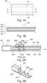
- Figure 1A shows a schematic top view on a flat band cable 100 that contains two conductors 101.
- the number of conductors is limited to two only for the purpose to simplify the illustration.
- a flat band cable normally contains more than two conductors.
- Figure 1B displays a cross-section through the flat band cable 100 along the line A-A' shown in Figure 1A .
- the conductor 101 is embedded between a lower and an upper insulating foil 102, 103.
- the lower and upper insulating foil 102, 103 are bonded onto the conductor 101 and to each other by a lower glue layer 105 and an upper glue layer 106, respectively.
- the combination of a glue layer and a foil will be named in the following as insulating layer.
- the thickness of an insulating layer ranges from 0,03 to 1 mm.
- the small thickness of the conductors in flat band cable requires a special contact technology for connecting a terminal or connector to the flat band cable and its conductors, respectively.
- the conductors of the flat band cable are contacted by a piercing contact that penetrates the conductor in the flat band cable.
- a single conductor may be penetrated by several piercing contacts to increase the stability of the mechanical connection between the flat band cable and the connector.
- the piercing contact penetrates through all layers shown in Figure 1B .
- the piercing contact may drag along particles of the lower foil and the lower glue layer that may have a negative impact on the electric properties of the contact between the conductor and the connector. In the worst case, there is no electrical contact between the connector and the conductor.
- a portion of the piercing contact is swaged on the flat band cable and scratches the upper foil 103 and the upper glue layer 106 and provides in this way for an additional contact area.
- the present disclosure suggests a flat band cable set comprising a flat band cable and a connector.
- the flat band cable comprises at least one conductor embedded between two insulating layers.
- the connector comprises a terminal and a contact portion with at least one piercing contact penetrating through the at least one conductor.
- a tip of the piercing contact is swaged.
- a swaged portion of the piercing contact enhances a mechanical and/or electrical connection between the flat band cable and the connector.
- One insulating layer adjacent to the at least one conductor is removed for offering an enlarged contact area on the at least one conductor for the swaged tip portion of the piercing contact.
- the suggested flat band cable set offers enhanced electrical properties over flat band cable sets with conventional crimp contacts without compromising mechanical stability of the contacts because the conductor of the flat band cable remains essentially intact.
- both insulating layers are removed from the flat band cable such the swaged portion of the piercing contact contacts one side of the conductor, and the contact portion of the connector contacts the other side of the conductor.
- the connector has been found useful in some embodiments to provide the connector with a plurality of piercing contacts.
- the number of piercing contacts can be adapted according to the required mechanical stability or electric properties of the contact.
- the insulating layer(s) is/are removed only below one swaged portion of one piercing contact. In this way, the mechanical stability of the connection between the connector and the flat band cable is impacted only to a very small extent by the removal of the insulating layer(s).
- the present disclosure suggests a method for manufacturing a flat band cable set.
- the method comprises
- the step of exposing the at least one conductor is implemented as stripping off one or both insulation layers of the flat band cable.
- the step of exposing the at least one conductor is implemented as providing windows in one or both insulation layers of the flat band cable during the manufacturing process of the flat band cable.
- This alternative implementation may have advantages in the manufacturing process in terms of costs.
- FIG. 2A illustrates a cross-section of a flat band cable set 200 comprising the flat band cable 100 and a connector 201.
- the connector 201 is a female single connector that is shown as an example. However, in other embodiments of the present disclosure other types of connectors are used. Integral parts of the connector 201 are a terminal 202 and a contact portion 203 that extends in Figure 2A below the flat band cable 100. From the contact portion 203 two piercing contacts 204a, 204b protrude and penetrate the flat band cable 100. A tip portion 205a, 205b of each piercing contact 204a, 204b is swaged onto the upper foil 103 such that a front end 206 of the tip portion 205 scratches away the upper foil 103.
- Figure 2B displays a perspective view of the connector 201.
- the terminal 202, the contact portion 203 and the piercing contacts 204a, 204b are shown in greater detail.
- the shown connector 201 is only an example.
- Other embodiments of the connector 201 have different forms of terminals 202 and only one or more than two piercing contacts.
- the piercing contacts can be arranged in a parallel or staggered manner or in any other way on the contact portion 203 of the connector 201. These possible variants of the connector are not essential for the implementation of the present disclosure.
- FIG 3 illustrates a flat band cable set 300 according to the present disclosure.
- the main difference of the cable set 300 shown in Figure 3 and the cable set 200 shown in Figure 2A is that on a free end of the flat band cable 100 the upper foil 102 and the upper glue layer 106 are stripped away along a distance d.
- the so exposed surface of the conductor 101 is in direct contact of the swaged tip portion 205a, 205b of the piercing contact 204a.
- the contact area between the swaged tip portion 205a and the conductor 101 is larger than the contact area between the piercing contact 204a and the conductor 101 in the flat band cable set 200 shown in Figure 2A . Consequently, the electrical properties of the electric contact between the terminal 201 and the conductor 101 in the flat band cable set 300 are improved compared to the flat band cable set 200 shown in Figure 2A .
- the tip portion 205b of the piercing contact 204b makes a U-turn and repenetrates both insulation layers and the conductor 101 of the flat band cable 100. This alternative embodiment is not shown in the drawing.
- FIG 4 a flat band cable set 400 according to the present disclosure is shown as an alternative embodiment.
- the flat band cable set 400 both insulating layers are stripped off along a distance d.
- a consequence of this difference is that when the piercing contact 204a is swaged, then the conductor 101 is bent down and comes in contact with the contact portion 203. Therefore, the contact area between the conductor 101 and the connector 201, specifically the contact area between the conductor and the piercing contact 204a, in flat band cable set 400 is even larger than in flat band cable set 300.
- piercing contact 204a is in contact with the surface(s) of conductor 101.
- more than one piercing contact may be in touch with the exposed surface(s) of conductor 101.
- the method for manufacturing a flat band cable set 300 or 400 includes as a first step S1 exposing at least one conductor 101 of the flat band cable 100.
- the step S1 of exposing the conductor 101 is realized in practice by stripping off one or both insulating layers of the flat band cable or by providing windows in one or both insulation layers of the flat band cable during the manufacturing process of the flat band cable, for instance. The selection of one of the alternatives may depend on properties of the flat band cable or requirements of the final product.
- the terminal 201 is pressed on the flat band cable 100 such that one or several piercing contacts 204a, 204b penetrate the conductor 101 of the flat band cable 100. Then, piercing contacts 204a, 204b are swaged such that at least one piercing contact 204a is in direct contact with an exposed surface of the conductor 101.
- a single unit or device may perform the functions of multiple elements recited in the claims.
- the fact that individual functions and elements are recited in different dependent claims does not mean that a combination of those functions and elements could not advantageously be used.
Landscapes
- Engineering & Computer Science (AREA)
- Manufacturing & Machinery (AREA)
- Coupling Device And Connection With Printed Circuit (AREA)
- Multi-Conductor Connections (AREA)
Abstract
A flat band cable set (300) comprising a flat band cable (100) and a connector (201) is suggested. The flat band cable comprises at least one conductor (101) embedded between two insulating layers (102-106). The connector (201) comprises a terminal (202) and a contact portion (203) with at least one piercing contact (204a,b) penetrating through the at least one conductor. A tip (205a,b) of the piercing contact is swaged. A swaged portion of the piercing contact enhances a mechanical and/or electrical connection between the flat band cable and the connector. One insulating layer (102-106) adjacent to the at least one conductor is removed over a predefined distance (d) for offering an enlarged contact area on the at least one conductor for the swaged tip portion of the piercing contact.
Description
- The present disclosure relates to a flat band cable set and a method for manufacturing a flat band cable set.
- Flat band cables such as flexible flat band cables (FFC) and flexible printed circuit boards (FPC) are frequently used to provide for a flexible and reliable connection between printed circuit boards. One area of application is in the automotive industry. Flat band cables are cost efficient and require only a limited installation space. All flat band cables have in common that they contain a multitude of conductors which are arranged in parallel in a flat configuration. The number of conductors may range from a few to above 20 conductors. The conductors are typically realized as a copper foil with a thickness ranging for instance from 35 to 100 µm. The conductors are embedded between two insulating layers.
-
Figure 1A shows a schematic top view on aflat band cable 100 that contains twoconductors 101. The number of conductors is limited to two only for the purpose to simplify the illustration. In reality, a flat band cable normally contains more than two conductors. -
Figure 1B displays a cross-section through theflat band cable 100 along the line A-A' shown inFigure 1A . as illustrated inFigure 1B theconductor 101 is embedded between a lower and an upperinsulating foil insulating foil conductor 101 and to each other by alower glue layer 105 and anupper glue layer 106, respectively. The combination of a glue layer and a foil will be named in the following as insulating layer. In practical embodiments the thickness of an insulating layer ranges from 0,03 to 1 mm. - The small thickness of the conductors in flat band cable requires a special contact technology for connecting a terminal or connector to the flat band cable and its conductors, respectively.
- According to a common approach the conductors of the flat band cable are contacted by a piercing contact that penetrates the conductor in the flat band cable. A single conductor may be penetrated by several piercing contacts to increase the stability of the mechanical connection between the flat band cable and the connector. In practice, the piercing contact penetrates through all layers shown in
Figure 1B . When penetrating through thelower foil 102 and thelower glue layer 105 the piercing contact may drag along particles of the lower foil and the lower glue layer that may have a negative impact on the electric properties of the contact between the conductor and the connector. In the worst case, there is no electrical contact between the connector and the conductor. In some types of crimp terminals for flat band cables, a portion of the piercing contact is swaged on the flat band cable and scratches theupper foil 103 and theupper glue layer 106 and provides in this way for an additional contact area. However, for some applications it is preferred to have a bigger contact area between the connector and the conductor of the flat band cable, for instance to increase reliability of the contact or its current carrying capability. - In view of the limitations of existing contact technologies for flat band cables there remains a desire for a modified contact technology to overcome or at least improve one or more of the problems mentioned at the outset.
- According to a first aspect the present disclosure suggests a flat band cable set comprising a flat band cable and a connector. The flat band cable comprises at least one conductor embedded between two insulating layers. The connector comprises a terminal and a contact portion with at least one piercing contact penetrating through the at least one conductor. A tip of the piercing contact is swaged. A swaged portion of the piercing contact enhances a mechanical and/or electrical connection between the flat band cable and the connector. One insulating layer adjacent to the at least one conductor is removed for offering an enlarged contact area on the at least one conductor for the swaged tip portion of the piercing contact.
- The suggested flat band cable set offers enhanced electrical properties over flat band cable sets with conventional crimp contacts without compromising mechanical stability of the contacts because the conductor of the flat band cable remains essentially intact.
- In an advantageous embodiment both insulating layers are removed from the flat band cable such the swaged portion of the piercing contact contacts one side of the conductor, and the contact portion of the connector contacts the other side of the conductor. By virtue of stripping off both insulating layers, the contact area between the conductor and the connector is further increased.
- It has been found useful in some embodiments to provide the connector with a plurality of piercing contacts. The number of piercing contacts can be adapted according to the required mechanical stability or electric properties of the contact.
- Advantageously, the insulating layer(s) is/are removed only below one swaged portion of one piercing contact. In this way, the mechanical stability of the connection between the connector and the flat band cable is impacted only to a very small extent by the removal of the insulating layer(s).
- According to a second aspect, the present disclosure suggests a method for manufacturing a flat band cable set. The method comprises
- exposing at least one conductor of a flat band cable;
- pressing a
connector 1 or several piercing contacts penetrate through the at least one conductor of the flat band cable; - swaging the piercing contacts such that at least one piercing contact is in direct contact with an exposed surface of the conductor.
- In one advantageous implementation of the method the step of exposing the at least one conductor is implemented as stripping off one or both insulation layers of the flat band cable.
- In an alternative implementation of the method the step of exposing the at least one conductor is implemented as providing windows in one or both insulation layers of the flat band cable during the manufacturing process of the flat band cable. This alternative implementation may have advantages in the manufacturing process in terms of costs.
- Exemplary embodiments of the present disclosure are illustrated in the drawings and are explained in more detail in the following description. In the figures, the same or similar elements are referenced with the same or similar reference signs. It shows:
- Fig. 1A
- a top view of a flat band cable;
- Fig. 1B
- a cross-section of the flat band cable shown in
Fig. 1A ; - Fig. 2A
- a conventional flat band cable set;
- Fig. 2B
- a connector of the flat band cable set shown in
figure 2A ; - Fig. 3
- a first embodiment of a flat band cable set according to the present disclosure;
- Fig. 4
- a second embodiment of the flat band cable set according to the present disclosure; and
- Fig. 5
- a flow diagram of a method for manufacturing a flat band cable set.
- In the figures the same or similar components are labelled with the same or similar reference signs. It is also noted that the dimensions, in particular the thickness of layers are exaggerated for the sake of clarity.
-
Figure 2A illustrates a cross-section of a flat band cable set 200 comprising theflat band cable 100 and aconnector 201. Theconnector 201 is a female single connector that is shown as an example. However, in other embodiments of the present disclosure other types of connectors are used. Integral parts of theconnector 201 are a terminal 202 and acontact portion 203 that extends inFigure 2A below theflat band cable 100. From thecontact portion 203 two piercingcontacts flat band cable 100. Atip portion contact upper foil 103 such that a front end 206 of the tip portion 205 scratches away theupper foil 103. -
Figure 2B displays a perspective view of theconnector 201. InFigure 2B the terminal 202, thecontact portion 203 and the piercingcontacts connector 201 is only an example. Other embodiments of theconnector 201 have different forms ofterminals 202 and only one or more than two piercing contacts. The piercing contacts can be arranged in a parallel or staggered manner or in any other way on thecontact portion 203 of theconnector 201. These possible variants of the connector are not essential for the implementation of the present disclosure. -
Figure 3 illustrates a flat band cable set 300 according to the present disclosure. The main difference of the cable set 300 shown inFigure 3 and the cable set 200 shown inFigure 2A is that on a free end of theflat band cable 100 theupper foil 102 and theupper glue layer 106 are stripped away along a distance d. The so exposed surface of theconductor 101 is in direct contact of the swagedtip portion contact 204a. Thus, the contact area between the swagedtip portion 205a and theconductor 101 is larger than the contact area between the piercingcontact 204a and theconductor 101 in the flat band cable set 200 shown inFigure 2A . Consequently, the electrical properties of the electric contact between the terminal 201 and theconductor 101 in the flat band cable set 300 are improved compared to the flat band cable set 200 shown inFigure 2A . - In an alternative embodiment of the flat band cable set 300 the
tip portion 205b of the piercingcontact 204b makes a U-turn and repenetrates both insulation layers and theconductor 101 of theflat band cable 100. This alternative embodiment is not shown in the drawing. - In
Figure 4 a flat band cable set 400 according to the present disclosure is shown as an alternative embodiment. In the flat band cable set 400 both insulating layers are stripped off along a distance d. A consequence of this difference is that when the piercingcontact 204a is swaged, then theconductor 101 is bent down and comes in contact with thecontact portion 203. Therefore, the contact area between theconductor 101 and theconnector 201, specifically the contact area between the conductor and the piercingcontact 204a, in flat band cable set 400 is even larger than in flatband cable set 300. - In the
Figures 3 and 4 only one piercing contact, namely piercingcontact 204a, is in contact with the surface(s) ofconductor 101. However, in other embodiments more than one piercing contact may be in touch with the exposed surface(s) ofconductor 101. - The method for manufacturing a flat band cable set 300 or 400 includes as a first step S1 exposing at least one
conductor 101 of theflat band cable 100. The step S1 of exposing theconductor 101 is realized in practice by stripping off one or both insulating layers of the flat band cable or by providing windows in one or both insulation layers of the flat band cable during the manufacturing process of the flat band cable, for instance. The selection of one of the alternatives may depend on properties of the flat band cable or requirements of the final product. In a next step S2, the terminal 201 is pressed on theflat band cable 100 such that one or several piercingcontacts conductor 101 of theflat band cable 100. Then, piercingcontacts contact 204a is in direct contact with an exposed surface of theconductor 101. - In the claims, the word "comprising" does not exclude other elements or steps, and the indefinite article "a" does not exclude a plurality.
- A single unit or device may perform the functions of multiple elements recited in the claims. The fact that individual functions and elements are recited in different dependent claims does not mean that a combination of those functions and elements could not advantageously be used.
-
- 100
- flat band cable
- 101
- conductor
- 102
- lower foil
- 103
- upper foil
- 105
- lower glue layer
- 106
- upper glue layer
- 200
- flat band cable set
- 201
- connector
- 202
- terminal
- 203
- contact portion
- 204a,b
- piercing contacts
- 205a,b
- tip portion of piercing contact
- 206
- front end of tip portion
- 300
- flat band cable set
- 301
- front end
- 400
- flat band cable set
Claims (7)
- Flat band cable set (300,400) comprising a flat band cable (100) and a connector (201), wherein the flat band cable (100) comprises at least one conductor (101) embedded between two insulating layers(102-106), wherein the connector (201) comprises a terminal (202) and a contact portion (203) with at least one piercing contact (204a,b) penetrating through the at least one conductor (101), wherein a tip (205a,b) of the piercing contact is swaged, wherein a swaged portion of the piercing contact enhances a mechanical and/or electrical connection between the flat band cable (300,400) and the connector characterized in that one insulating layer (102-106) adjacent to the at least one conductor (101) is removed for offering an enlarged contact area on the at least one conductor for the swaged tip portion of the piercing contact.
- Flat band cable set according to claim 1, wherein both insulating layers (102-106) are removed such the swaged portion (205a,205b) of the piercing contact (204a,204b) contacts one side of the conductor (101) and the contact portion (203) of the connector contacts the other side of the conductor.
- Flat band cable set according to claim 1, wherein the connector comprises a plurality of piercing contacts (204a,b).
- Flat band cable set according to one of the preceding claims, wherein the insulating layer (120-106) is removed only below one swaged portion (205a,205b) of one piercing contact.
- Method for manufacturing a flat band cable set, wherein the method comprises- exposing (S1) at least one conductor (101) of a flat band cable (100);- pressing (S2) a connector (201) onto the flat band cable (100) such that one or several piercing contacts (204a,b) penetrate through the at least one conductor (101) of the flat band cable;- swaging the piercing contacts (204a,b) such that at least one piercing contact is in direct contact with an exposed surface of the conductor (101).
- Method for manufacturing a flat band cable set according to claim 5, wherein exposing (S1) the at least one conductor is implemented as stripping off one or both insulation layers of the flat band cable.
- Method for manufacturing a flat band cable set according to claim 5, wherein exposing (S1) the at least one conductor is implemented as providing windows in one or both insulation layers of the flat band cable during the manufacturing process of the flat band cable.
Priority Applications (1)
| Application Number | Priority Date | Filing Date | Title |
|---|---|---|---|
| EP22306457.7A EP4346012A1 (en) | 2022-09-30 | 2022-09-30 | Flat band cable set and method for manufacturing a flat band cable set |
Applications Claiming Priority (1)
| Application Number | Priority Date | Filing Date | Title |
|---|---|---|---|
| EP22306457.7A EP4346012A1 (en) | 2022-09-30 | 2022-09-30 | Flat band cable set and method for manufacturing a flat band cable set |
Publications (1)
| Publication Number | Publication Date |
|---|---|
| EP4346012A1 true EP4346012A1 (en) | 2024-04-03 |
Family
ID=83691650
Family Applications (1)
| Application Number | Title | Priority Date | Filing Date |
|---|---|---|---|
| EP22306457.7A Withdrawn EP4346012A1 (en) | 2022-09-30 | 2022-09-30 | Flat band cable set and method for manufacturing a flat band cable set |
Country Status (1)
| Country | Link |
|---|---|
| EP (1) | EP4346012A1 (en) |
Citations (4)
| Publication number | Priority date | Publication date | Assignee | Title |
|---|---|---|---|---|
| JP2003203703A (en) * | 2002-01-09 | 2003-07-18 | Auto Network Gijutsu Kenkyusho:Kk | Connection method and connection structure of terminal and flat wiring material |
| JP2005190719A (en) * | 2003-12-24 | 2005-07-14 | Fujikura Ltd | Connection terminal connection structure |
| EP1691452A2 (en) * | 2002-12-18 | 2006-08-16 | Yazaki Corporation | Connecting member for flat circuit member and method of connecting the connecting member and the flat circuit member |
| JP2006222057A (en) * | 2005-01-13 | 2006-08-24 | Furukawa Electric Co Ltd:The | Connection structure of flexible flat electrical structure |
-
2022
- 2022-09-30 EP EP22306457.7A patent/EP4346012A1/en not_active Withdrawn
Patent Citations (4)
| Publication number | Priority date | Publication date | Assignee | Title |
|---|---|---|---|---|
| JP2003203703A (en) * | 2002-01-09 | 2003-07-18 | Auto Network Gijutsu Kenkyusho:Kk | Connection method and connection structure of terminal and flat wiring material |
| EP1691452A2 (en) * | 2002-12-18 | 2006-08-16 | Yazaki Corporation | Connecting member for flat circuit member and method of connecting the connecting member and the flat circuit member |
| JP2005190719A (en) * | 2003-12-24 | 2005-07-14 | Fujikura Ltd | Connection terminal connection structure |
| JP2006222057A (en) * | 2005-01-13 | 2006-08-24 | Furukawa Electric Co Ltd:The | Connection structure of flexible flat electrical structure |
Similar Documents
| Publication | Publication Date | Title |
|---|---|---|
| US6931727B2 (en) | Method of connecting multi conductor cable connector | |
| US6799990B2 (en) | Crimp connector | |
| CN107683548A (en) | Low Profile Electrical Connector | |
| US4749365A (en) | Insulation displacement terminal | |
| US20050250356A1 (en) | Press-fit terminal and circuit board module using the same | |
| JPS6380492A (en) | Wiring of connector | |
| US3880488A (en) | Electrical connector to connect to flat flexible cable | |
| KR101077361B1 (en) | Pressure connection structure with coaxial cable | |
| US4302065A (en) | Flat cable assembly and methods of terminating and connectorizing the cable of same | |
| US6371805B1 (en) | Cable assembly and method for making the same | |
| KR101521386B1 (en) | Method of connecting a cable with a cable connector | |
| JP2009037748A (en) | Cable connector and cable connection method | |
| KR100604118B1 (en) | Connector assuring more reliable connection of a cable | |
| CN1412895A (en) | Connector for flexible circuit board | |
| JP2006019025A (en) | connector | |
| JPS6244457Y2 (en) | ||
| EP4346013B1 (en) | Connector, connector assembly, and connecting method | |
| JP4807796B2 (en) | Cable connector and cable connection method | |
| JP3275537B2 (en) | Modular plug | |
| KR20050049401A (en) | Piercing terminal for coaxial cable | |
| JPH11232932A (en) | Flat cable assembly and flat cable used therein | |
| JPH0638334Y2 (en) | Flat cable with shield | |
| EP1408586A1 (en) | Crimp connector | |
| CN120049216A (en) | Conductor press-connection structure for connecting terminal | |
| JPS63269465A (en) | Flat cable with crimp terminal |
Legal Events
| Date | Code | Title | Description |
|---|---|---|---|
| PUAI | Public reference made under article 153(3) epc to a published international application that has entered the european phase |
Free format text: ORIGINAL CODE: 0009012 |
|
| STAA | Information on the status of an ep patent application or granted ep patent |
Free format text: STATUS: THE APPLICATION HAS BEEN PUBLISHED |
|
| AK | Designated contracting states |
Kind code of ref document: A1 Designated state(s): AL AT BE BG CH CY CZ DE DK EE ES FI FR GB GR HR HU IE IS IT LI LT LU LV MC MK MT NL NO PL PT RO RS SE SI SK SM TR |
|
| STAA | Information on the status of an ep patent application or granted ep patent |
Free format text: STATUS: THE APPLICATION IS DEEMED TO BE WITHDRAWN |
|
| 18D | Application deemed to be withdrawn |
Effective date: 20241005 |