EP4345892A1 - Semiconductor device with resin bleed control structure and method therefor - Google Patents
Semiconductor device with resin bleed control structure and method therefor Download PDFInfo
- Publication number
- EP4345892A1 EP4345892A1 EP23199798.2A EP23199798A EP4345892A1 EP 4345892 A1 EP4345892 A1 EP 4345892A1 EP 23199798 A EP23199798 A EP 23199798A EP 4345892 A1 EP4345892 A1 EP 4345892A1
- Authority
- EP
- European Patent Office
- Prior art keywords
- die pad
- die
- ridges
- ridge
- pad
- Prior art date
- Legal status (The legal status is an assumption and is not a legal conclusion. Google has not performed a legal analysis and makes no representation as to the accuracy of the status listed.)
- Withdrawn
Links
Images




Classifications
-
- H—ELECTRICITY
- H10—SEMICONDUCTOR DEVICES; ELECTRIC SOLID-STATE DEVICES NOT OTHERWISE PROVIDED FOR
- H10W—GENERIC PACKAGES, INTERCONNECTIONS, CONNECTORS OR OTHER CONSTRUCTIONAL DETAILS OF DEVICES COVERED BY CLASS H10
- H10W70/00—Package substrates; Interposers; Redistribution layers [RDL]
- H10W70/40—Leadframes
- H10W70/421—Shapes or dispositions
- H10W70/424—Cross-sectional shapes
- H10W70/427—Bent parts
-
- H—ELECTRICITY
- H10—SEMICONDUCTOR DEVICES; ELECTRIC SOLID-STATE DEVICES NOT OTHERWISE PROVIDED FOR
- H10W—GENERIC PACKAGES, INTERCONNECTIONS, CONNECTORS OR OTHER CONSTRUCTIONAL DETAILS OF DEVICES COVERED BY CLASS H10
- H10W70/00—Package substrates; Interposers; Redistribution layers [RDL]
- H10W70/01—Manufacture or treatment
- H10W70/04—Manufacture or treatment of leadframes
-
- H—ELECTRICITY
- H10—SEMICONDUCTOR DEVICES; ELECTRIC SOLID-STATE DEVICES NOT OTHERWISE PROVIDED FOR
- H10W—GENERIC PACKAGES, INTERCONNECTIONS, CONNECTORS OR OTHER CONSTRUCTIONAL DETAILS OF DEVICES COVERED BY CLASS H10
- H10W70/00—Package substrates; Interposers; Redistribution layers [RDL]
- H10W70/01—Manufacture or treatment
- H10W70/04—Manufacture or treatment of leadframes
- H10W70/048—Mechanical treatments, e.g. punching, cutting, deforming or cold welding
-
- H—ELECTRICITY
- H10—SEMICONDUCTOR DEVICES; ELECTRIC SOLID-STATE DEVICES NOT OTHERWISE PROVIDED FOR
- H10W—GENERIC PACKAGES, INTERCONNECTIONS, CONNECTORS OR OTHER CONSTRUCTIONAL DETAILS OF DEVICES COVERED BY CLASS H10
- H10W70/00—Package substrates; Interposers; Redistribution layers [RDL]
- H10W70/40—Leadframes
- H10W70/411—Chip-supporting parts, e.g. die pads
- H10W70/417—Bonding materials between chips and die pads
-
- H—ELECTRICITY
- H10—SEMICONDUCTOR DEVICES; ELECTRIC SOLID-STATE DEVICES NOT OTHERWISE PROVIDED FOR
- H10W—GENERIC PACKAGES, INTERCONNECTIONS, CONNECTORS OR OTHER CONSTRUCTIONAL DETAILS OF DEVICES COVERED BY CLASS H10
- H10W70/00—Package substrates; Interposers; Redistribution layers [RDL]
- H10W70/40—Leadframes
- H10W70/421—Shapes or dispositions
- H10W70/424—Cross-sectional shapes
-
- H—ELECTRICITY
- H10—SEMICONDUCTOR DEVICES; ELECTRIC SOLID-STATE DEVICES NOT OTHERWISE PROVIDED FOR
- H10W—GENERIC PACKAGES, INTERCONNECTIONS, CONNECTORS OR OTHER CONSTRUCTIONAL DETAILS OF DEVICES COVERED BY CLASS H10
- H10W70/00—Package substrates; Interposers; Redistribution layers [RDL]
- H10W70/40—Leadframes
- H10W70/421—Shapes or dispositions
- H10W70/438—Shapes or dispositions of side rails, e.g. having holes
-
- H—ELECTRICITY
- H10—SEMICONDUCTOR DEVICES; ELECTRIC SOLID-STATE DEVICES NOT OTHERWISE PROVIDED FOR
- H10W—GENERIC PACKAGES, INTERCONNECTIONS, CONNECTORS OR OTHER CONSTRUCTIONAL DETAILS OF DEVICES COVERED BY CLASS H10
- H10W70/00—Package substrates; Interposers; Redistribution layers [RDL]
- H10W70/40—Leadframes
- H10W70/464—Additional interconnections in combination with leadframes
- H10W70/465—Bumps or wires
-
- H—ELECTRICITY
- H10—SEMICONDUCTOR DEVICES; ELECTRIC SOLID-STATE DEVICES NOT OTHERWISE PROVIDED FOR
- H10W—GENERIC PACKAGES, INTERCONNECTIONS, CONNECTORS OR OTHER CONSTRUCTIONAL DETAILS OF DEVICES COVERED BY CLASS H10
- H10W72/00—Interconnections or connectors in packages
- H10W72/071—Connecting or disconnecting
-
- H—ELECTRICITY
- H10—SEMICONDUCTOR DEVICES; ELECTRIC SOLID-STATE DEVICES NOT OTHERWISE PROVIDED FOR
- H10W—GENERIC PACKAGES, INTERCONNECTIONS, CONNECTORS OR OTHER CONSTRUCTIONAL DETAILS OF DEVICES COVERED BY CLASS H10
- H10W72/00—Interconnections or connectors in packages
- H10W72/30—Die-attach connectors
-
- H—ELECTRICITY
- H10—SEMICONDUCTOR DEVICES; ELECTRIC SOLID-STATE DEVICES NOT OTHERWISE PROVIDED FOR
- H10W—GENERIC PACKAGES, INTERCONNECTIONS, CONNECTORS OR OTHER CONSTRUCTIONAL DETAILS OF DEVICES COVERED BY CLASS H10
- H10W72/00—Interconnections or connectors in packages
- H10W72/50—Bond wires
-
- H—ELECTRICITY
- H10—SEMICONDUCTOR DEVICES; ELECTRIC SOLID-STATE DEVICES NOT OTHERWISE PROVIDED FOR
- H10W—GENERIC PACKAGES, INTERCONNECTIONS, CONNECTORS OR OTHER CONSTRUCTIONAL DETAILS OF DEVICES COVERED BY CLASS H10
- H10W72/00—Interconnections or connectors in packages
- H10W72/851—Dispositions of multiple connectors or interconnections
-
- H—ELECTRICITY
- H10—SEMICONDUCTOR DEVICES; ELECTRIC SOLID-STATE DEVICES NOT OTHERWISE PROVIDED FOR
- H10W—GENERIC PACKAGES, INTERCONNECTIONS, CONNECTORS OR OTHER CONSTRUCTIONAL DETAILS OF DEVICES COVERED BY CLASS H10
- H10W74/00—Encapsulations, e.g. protective coatings
- H10W74/10—Encapsulations, e.g. protective coatings characterised by their shape or disposition
- H10W74/111—Encapsulations, e.g. protective coatings characterised by their shape or disposition the semiconductor body being completely enclosed
- H10W74/129—Encapsulations, e.g. protective coatings characterised by their shape or disposition the semiconductor body being completely enclosed forming a chip-scale package [CSP]
-
- H—ELECTRICITY
- H10—SEMICONDUCTOR DEVICES; ELECTRIC SOLID-STATE DEVICES NOT OTHERWISE PROVIDED FOR
- H10W—GENERIC PACKAGES, INTERCONNECTIONS, CONNECTORS OR OTHER CONSTRUCTIONAL DETAILS OF DEVICES COVERED BY CLASS H10
- H10W90/00—Package configurations
- H10W90/811—Multiple chips on leadframes
-
- H—ELECTRICITY
- H10—SEMICONDUCTOR DEVICES; ELECTRIC SOLID-STATE DEVICES NOT OTHERWISE PROVIDED FOR
- H10W—GENERIC PACKAGES, INTERCONNECTIONS, CONNECTORS OR OTHER CONSTRUCTIONAL DETAILS OF DEVICES COVERED BY CLASS H10
- H10W99/00—Subject matter not provided for in other groups of this subclass
-
- H—ELECTRICITY
- H10—SEMICONDUCTOR DEVICES; ELECTRIC SOLID-STATE DEVICES NOT OTHERWISE PROVIDED FOR
- H10W—GENERIC PACKAGES, INTERCONNECTIONS, CONNECTORS OR OTHER CONSTRUCTIONAL DETAILS OF DEVICES COVERED BY CLASS H10
- H10W72/00—Interconnections or connectors in packages
- H10W72/071—Connecting or disconnecting
- H10W72/073—Connecting or disconnecting of die-attach connectors
-
- H—ELECTRICITY
- H10—SEMICONDUCTOR DEVICES; ELECTRIC SOLID-STATE DEVICES NOT OTHERWISE PROVIDED FOR
- H10W—GENERIC PACKAGES, INTERCONNECTIONS, CONNECTORS OR OTHER CONSTRUCTIONAL DETAILS OF DEVICES COVERED BY CLASS H10
- H10W72/00—Interconnections or connectors in packages
- H10W72/071—Connecting or disconnecting
- H10W72/075—Connecting or disconnecting of bond wires
-
- H—ELECTRICITY
- H10—SEMICONDUCTOR DEVICES; ELECTRIC SOLID-STATE DEVICES NOT OTHERWISE PROVIDED FOR
- H10W—GENERIC PACKAGES, INTERCONNECTIONS, CONNECTORS OR OTHER CONSTRUCTIONAL DETAILS OF DEVICES COVERED BY CLASS H10
- H10W72/00—Interconnections or connectors in packages
- H10W72/071—Connecting or disconnecting
- H10W72/075—Connecting or disconnecting of bond wires
- H10W72/07551—Connecting or disconnecting of bond wires characterised by changes in properties of the bond wires during the connecting
- H10W72/07554—Connecting or disconnecting of bond wires characterised by changes in properties of the bond wires during the connecting changes in dispositions
-
- H—ELECTRICITY
- H10—SEMICONDUCTOR DEVICES; ELECTRIC SOLID-STATE DEVICES NOT OTHERWISE PROVIDED FOR
- H10W—GENERIC PACKAGES, INTERCONNECTIONS, CONNECTORS OR OTHER CONSTRUCTIONAL DETAILS OF DEVICES COVERED BY CLASS H10
- H10W72/00—Interconnections or connectors in packages
- H10W72/30—Die-attach connectors
- H10W72/351—Materials of die-attach connectors
- H10W72/353—Materials of die-attach connectors not comprising solid metals or solid metalloids, e.g. ceramics
- H10W72/354—Materials of die-attach connectors not comprising solid metals or solid metalloids, e.g. ceramics comprising polymers
-
- H—ELECTRICITY
- H10—SEMICONDUCTOR DEVICES; ELECTRIC SOLID-STATE DEVICES NOT OTHERWISE PROVIDED FOR
- H10W—GENERIC PACKAGES, INTERCONNECTIONS, CONNECTORS OR OTHER CONSTRUCTIONAL DETAILS OF DEVICES COVERED BY CLASS H10
- H10W72/00—Interconnections or connectors in packages
- H10W72/50—Bond wires
- H10W72/531—Shapes of wire connectors
- H10W72/536—Shapes of wire connectors the connected ends being ball-shaped
-
- H—ELECTRICITY
- H10—SEMICONDUCTOR DEVICES; ELECTRIC SOLID-STATE DEVICES NOT OTHERWISE PROVIDED FOR
- H10W—GENERIC PACKAGES, INTERCONNECTIONS, CONNECTORS OR OTHER CONSTRUCTIONAL DETAILS OF DEVICES COVERED BY CLASS H10
- H10W72/00—Interconnections or connectors in packages
- H10W72/50—Bond wires
- H10W72/531—Shapes of wire connectors
- H10W72/5363—Shapes of wire connectors the connected ends being wedge-shaped
-
- H—ELECTRICITY
- H10—SEMICONDUCTOR DEVICES; ELECTRIC SOLID-STATE DEVICES NOT OTHERWISE PROVIDED FOR
- H10W—GENERIC PACKAGES, INTERCONNECTIONS, CONNECTORS OR OTHER CONSTRUCTIONAL DETAILS OF DEVICES COVERED BY CLASS H10
- H10W72/00—Interconnections or connectors in packages
- H10W72/50—Bond wires
- H10W72/551—Materials of bond wires
- H10W72/552—Materials of bond wires comprising metals or metalloids, e.g. silver
-
- H—ELECTRICITY
- H10—SEMICONDUCTOR DEVICES; ELECTRIC SOLID-STATE DEVICES NOT OTHERWISE PROVIDED FOR
- H10W—GENERIC PACKAGES, INTERCONNECTIONS, CONNECTORS OR OTHER CONSTRUCTIONAL DETAILS OF DEVICES COVERED BY CLASS H10
- H10W72/00—Interconnections or connectors in packages
- H10W72/50—Bond wires
- H10W72/551—Materials of bond wires
- H10W72/552—Materials of bond wires comprising metals or metalloids, e.g. silver
- H10W72/5522—Materials of bond wires comprising metals or metalloids, e.g. silver comprising gold [Au]
-
- H—ELECTRICITY
- H10—SEMICONDUCTOR DEVICES; ELECTRIC SOLID-STATE DEVICES NOT OTHERWISE PROVIDED FOR
- H10W—GENERIC PACKAGES, INTERCONNECTIONS, CONNECTORS OR OTHER CONSTRUCTIONAL DETAILS OF DEVICES COVERED BY CLASS H10
- H10W72/00—Interconnections or connectors in packages
- H10W72/50—Bond wires
- H10W72/551—Materials of bond wires
- H10W72/552—Materials of bond wires comprising metals or metalloids, e.g. silver
- H10W72/5525—Materials of bond wires comprising metals or metalloids, e.g. silver comprising copper [Cu]
-
- H—ELECTRICITY
- H10—SEMICONDUCTOR DEVICES; ELECTRIC SOLID-STATE DEVICES NOT OTHERWISE PROVIDED FOR
- H10W—GENERIC PACKAGES, INTERCONNECTIONS, CONNECTORS OR OTHER CONSTRUCTIONAL DETAILS OF DEVICES COVERED BY CLASS H10
- H10W72/00—Interconnections or connectors in packages
- H10W72/851—Dispositions of multiple connectors or interconnections
- H10W72/874—On different surfaces
- H10W72/884—Die-attach connectors and bond wires
-
- H—ELECTRICITY
- H10—SEMICONDUCTOR DEVICES; ELECTRIC SOLID-STATE DEVICES NOT OTHERWISE PROVIDED FOR
- H10W—GENERIC PACKAGES, INTERCONNECTIONS, CONNECTORS OR OTHER CONSTRUCTIONAL DETAILS OF DEVICES COVERED BY CLASS H10
- H10W74/00—Encapsulations, e.g. protective coatings
- H10W74/01—Manufacture or treatment
-
- H—ELECTRICITY
- H10—SEMICONDUCTOR DEVICES; ELECTRIC SOLID-STATE DEVICES NOT OTHERWISE PROVIDED FOR
- H10W—GENERIC PACKAGES, INTERCONNECTIONS, CONNECTORS OR OTHER CONSTRUCTIONAL DETAILS OF DEVICES COVERED BY CLASS H10
- H10W74/00—Encapsulations, e.g. protective coatings
- H10W74/10—Encapsulations, e.g. protective coatings characterised by their shape or disposition
- H10W74/111—Encapsulations, e.g. protective coatings characterised by their shape or disposition the semiconductor body being completely enclosed
-
- H—ELECTRICITY
- H10—SEMICONDUCTOR DEVICES; ELECTRIC SOLID-STATE DEVICES NOT OTHERWISE PROVIDED FOR
- H10W—GENERIC PACKAGES, INTERCONNECTIONS, CONNECTORS OR OTHER CONSTRUCTIONAL DETAILS OF DEVICES COVERED BY CLASS H10
- H10W90/00—Package configurations
- H10W90/701—Package configurations characterised by the relative positions of pads or connectors relative to package parts
- H10W90/731—Package configurations characterised by the relative positions of pads or connectors relative to package parts of die-attach connectors
- H10W90/736—Package configurations characterised by the relative positions of pads or connectors relative to package parts of die-attach connectors between a chip and a stacked lead frame, conducting package substrate or heat sink
-
- H—ELECTRICITY
- H10—SEMICONDUCTOR DEVICES; ELECTRIC SOLID-STATE DEVICES NOT OTHERWISE PROVIDED FOR
- H10W—GENERIC PACKAGES, INTERCONNECTIONS, CONNECTORS OR OTHER CONSTRUCTIONAL DETAILS OF DEVICES COVERED BY CLASS H10
- H10W90/00—Package configurations
- H10W90/701—Package configurations characterised by the relative positions of pads or connectors relative to package parts
- H10W90/751—Package configurations characterised by the relative positions of pads or connectors relative to package parts of bond wires
- H10W90/756—Package configurations characterised by the relative positions of pads or connectors relative to package parts of bond wires between a chip and a stacked lead frame, conducting package substrate or heat sink
Definitions
- This disclosure relates generally to semiconductor devices, and more specifically, to semiconductor device with resin bleed control structure and method of forming the same.
- a semiconductor device having a resin bleed control structure includes a semiconductor die mounted on a package leadframe having a plurality of conductive leads.
- the package leadframe includes a die pad surrounded by the plurality of conductive leads.
- the die pad of the leadframe is configured with a plurality of ridges formed at outer edges of the die pad.
- Each ridge is a structure (e.g., vertical wall) formed at each outer edge of the die pad during the stamping process of the leadframe, for example.
- Each ridge is configured to control resin bleed from a die attach material by preventing the resin bleed from reaching a backside of the die pad.
- FIG. 1 illustrates, in a simplified plan view, an example semiconductor device package leadframe 100 having resin bleed control structures at a stage of manufacture in accordance with an embodiment.
- the package leadframe 100 includes a die pad 102, a plurality of resin bleed control structures formed as ridges 104 at the outer edges of the die pad, a plurality of conductive leads 106 surrounding the die pad, tie bars 108, through openings 110 adjacent to outer edges of the plurality of ridges, and mold lock rails 112 connected to the tie bars and the die pad.
- the plurality of ridges 104 is configured to arrest or impede resin bleed from a die attach material employed to attach a semiconductor die to the die pad 102.
- the die pad may be susceptible to resin bleed (e.g., from a die attach adhesive) contamination at the backside of the die pad.
- the die attach material may "bleed" a resin material in a direction away from an attached die region toward the outer edges of the die pad.
- the resin bleed may eventually reach the backside of the die pad allowing the resin to contaminate handling equipment and subsequently contaminate other leadframes in a manufacturing flow.
- contamination may lead to reduced product quality and lower production yields.
- Design rules have been incorporated to mitigate contamination by keeping the attached die region further away from the die pad edges. With such design rules, however, leadframes with larger die pads are likely required. In turn, larger device packages may be needed to accommodate leadframes with larger die pads.
- the plurality of ridges 104 of the package leadframe 100 serve as resin bleed control structures by impeding resin bleed flow and thus, preventing resin bleed from reaching the backside of the die pad 102.
- the package leadframe 100 incorporates resin bleed control features (e.g., ridges 104) of the die pad 102 configured to prevent resin bleed contamination without significant impact to the size of the die pad 102 or overall size of the package leadframe 100.
- the package leadframe 100 may be formed from suitable electrically conductive materials, such as copper, silver, nickel, aluminum, or iron, or alloys thereof, for example.
- the conductive metal may be bare, partially plated, or plated with another metal or an alloy such as iron/nickel alloy, silver, gold, copper, or the like.
- the term "conductive,” as used herein, generally refers to electrical conductivity unless otherwise specified.
- Cross-sectional views of semiconductor device package leadframe 100 taken along line A-A are shown in example stages of manufacture depicted in FIG. 2 and FIG. 3 .
- the die pad 102 may be formed having any suitable shape or size.
- each ridge 104 is formed at an outer edge of the die pad 102.
- a die attach region of the die pad 102 is essentially defined as a perimeter formed by the inner sidewalls of the ridges 104. Accordingly, the die attach region of the die pad is configured for an attachment of a semiconductor die such that the semiconductor die is substantially surrounded by the plurality of ridges 104.
- the plurality of leads 106 are configured and arranged to couple electrical signals between external (e.g., printed circuit board) locations of a mounted semiconductor device and internal locations such as bond pads on a semiconductor die attached to the die pad 102, for example.
- through openings 110 are formed immediately adjacent to outer edges of the plurality of ridges.
- the openings 110 allow improved flow of a molding compound through the leadframe during a molding operation, for example.
- the mold lock rails 112 are formed at an outer perimeter of the openings 112 allowing the molding compound to further lock onto the leadframe as it cures.
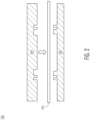
- FIG. 2 illustrates, in a simplified cross-sectional view, the example semiconductor device package leadframe 100 taken along line A-A at a stage of manufacture in accordance with an embodiment.
- a leadframe blank 202 is positioned in a leadframe stamping apparatus.
- the leadframe blank 202 may be in the form of a metal sheet or metal strip which is fed into the stamping apparatus.
- the stamping apparatus may include a punch fixture 204 and a die fixture 206, for example, configured to punch out portions (e.g., openings 110, spaces between leads 106) of the metal and bend portions (e.g., ridges 104) of the metal to form features of the package leadframe 100 during a leadframe stamping operation.
- FIG. 3 illustrates, in a simplified cross-sectional view, the example semiconductor device package leadframe 100 taken along line A-A at a subsequent stage of manufacture in accordance with an embodiment.
- the resulting package leadframe 100 from the stamping operation includes the die pad 102 and the ridges 104 formed at the outer edges, through openings 110 formed adjacent to outer edges of the ridges 104, mold lock rails 112 formed between the openings 110 and the conductive leads 106 surrounding the die pad.
- the package leadframe 100 may be bare, partially plated, or plated with another metal or alloy at this stage.
- the plurality of ridges 104 are formed by bending the die pad metal at the outer edges of the die pad 102 as a product of the leadframe stamping operation.
- a ridge 104 is formed at each of the four major outer edges of the die pad 102 as a series of four separate ridge segments located around an outer edge perimeter of the die pad 102.
- no ridge structure is formed in corners of the die pad 102.
- each ridge 104 is formed as a vertical wall substantially perpendicular to the plane of the die pad 102.
- each ridge 104 may be formed at an angle greater than 90 degrees relative to the plane of the die pad 102.
- Each ridge 104 has a predetermined height dimension 302 measured from the plane at the top surface of the die pad 102 and a predetermined thickness dimension 304 based on the thickness 306 of the die pad 102.
- the height dimension 302 may be in a range of 5-100 microns or higher, and the thickness dimension 304 may be in a range of 10-100% of the die pad thickness 306.
- the height and thickness dimensions (302 and 304) are chosen for a ridge configuration to substantially arrest resin bleed which may occur from a die attach material used in a manufacture of a semiconductor device.
- FIG. 4 through FIG. 6 illustrate, in simplified cross-sectional views, an example semiconductor device 400 at stages of manufacture in accordance with an embodiment.
- the stages of manufacture of the semiconductor device 400 depicted in FIG. 4 through FIG. 6 include the example package leadframe 100 taken along line A-A shown in FIG. 1 .
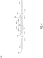
- FIG. 4 illustrates, in a simplified cross-sectional view, the example semiconductor device 400 taken along line A-A at a stage of manufacture in accordance with an embodiment.
- a semiconductor die 402 is attached to the die pad 102 of the package leadframe 100.
- the semiconductor die 402 is attached to the die pad 102 by way of a die attach material 406.
- the die attach material 406 may be an epoxy resin based adhesive material, for example.
- the ridges 104 are configured to substantially surround the attached semiconductor die 402 and block resin bleed from reaching the backside of the die pad 102. Accordingly, the formed ridges 104 at outer edges of the die pad 102 may be characterized as a resin bleed control structures.
- the semiconductor die 402 has an active side (e.g., major side having circuitry, bond pads) and a backside (e.g., major side opposite of the active side).
- the semiconductor die 402 includes bond pads 404 located at the active side of the semiconductor die.
- the bond pads 404 may be configured for connection to respective leadframe leads 106 by way of bond wires (attached at a subsequent stage), for example.
- semiconductor die 402 is configured in an active-side-up orientation.
- the semiconductor die 402 may be formed from any suitable semiconductor material, such as silicon, germanium, gallium arsenide, gallium nitride, and the like.
- the semiconductor die 402 may further include any digital circuits, analog circuits, RF circuits, memory, processor, the like, and combinations thereof at the active side.
- FIG. 5 illustrates, in a simplified cross-sectional view, the example semiconductor device 400 taken along line A-A at a subsequent stage of manufacture in accordance with an embodiment.
- the semiconductor device 400 includes bond wires 502 interconnecting the semiconductor die 402 with respective conductive leads 106 of the leadframe 100.
- a ball bond is formed at respective bond pads 404 with a first end of the bond wire 502 and a wedge bond is formed on the corresponding conductive lead 106 with a second end of the bond wire 502.
- the bond wires 502 may be formed from a suitable metal material such as copper, silver, gold, or alloys thereof, for example.
- FIG. 6 illustrates, in a simplified cross-sectional view, the example semiconductor device 400 taken along line A-A at a subsequent stage of manufacture in accordance with an embodiment.
- the semiconductor device 400 includes an encapsulant 602 encapsulating the semiconductor die 402, the die pad 108 and ridges 104, and portions of the leads 106.
- the encapsulant 602 may be an epoxy molding compound dispensed during an injection molding encapsulation operation, for example. Portions of the leads 106 outside of the encapsulated region of the semiconductor device 400 are not shown for illustration purposes.
- the semiconductor device 400 may be singulated into individual devices with leads 106 trimmed and formed into a configuration suitable for attachment to a printed circuit board, for example.
- a method including forming a package leadframe, the package leadframe including a die pad including a first ridge formed at a first outer edge of the die pad; a second ridge formed at a second outer edge of the die pad opposite of the first outer edge, each of the first and second ridges separate from one another; a plurality of leads surrounding the die pad; attaching a semiconductor die to the die pad by way of a die attach material, the semiconductor die located between the first ridge and the second ridge; and encapsulating with an encapsulant the semiconductor die and at least a portion of the package leadframe.
- the method may further include before encapsulating with the encapsulant, attaching a first end of a bond wire to a bond pad of the semiconductor die and a second end of the bond wire to a lead of the plurality of leads.
- the first and second ridges may be formed from a same metal material as the die pad.
- the first and second ridges may be formed by bending the respective outer edges of the die pad such that the first and second ridges are substantially perpendicular to a plane of the die pad.
- the first and second ridges may be configured to arrest resin bleed from the die attach material.
- the package leadframe may further include an opening through the package leadframe immediately adjacent to an outer edge of each of the first and second ridges.
- the die pad may further include a third ridge formed at a third outer edge of the die pad, the third out edge different from the first and second outer edges; and a fourth ridge formed at a fourth outer edge of the die pad opposite of the third outer edge, each of the first, second, third, and fourth ridges separate from one another.
- the first and second ridges may be formed such that a top edge of the first and second ridges extends above the plane of the die pad by 5 microns or greater.
- the first and second ridges may be formed such that a thickness of each of the first and second ridges is in a range of 10% to 100% of the thickness of the die pad.
- a semiconductor device including a package leadframe including a die pad and a plurality of leads, a plurality of ridges formed at outer edges of the die pad and configured to arrest resin bleed from a die attach material; a semiconductor die attached to the die pad of the package leadframe by way of the die attach material; a bond wire having a first end connected to a bond pad of the semiconductor die and a second end connected to a lead of the plurality of leads; and an encapsulant encapsulating the semiconductor die and at least a portion of the package leadframe.
- Each ridge of the plurality of ridges may be formed from a same metal material as the die pad.
- Each ridge of the plurality of ridges may be bent portion of the respective outer edges of the die pad such each ridge is substantially perpendicular to a plane of the die pad.
- the package leadframe may further include an opening through the package leadframe immediately adjacent to an outer edge of each ridge of the plurality of ridges.
- Each ridge of the plurality of ridges may be formed such that a top edge of each ridge extends above the plane of the die pad by 5 microns or greater.
- Each ridge of the plurality of ridges may be formed such that a thickness of each ridge is in a range of 10% to 100% of the thickness of the die pad.
- a method including forming a package leadframe, the package leadframe including a die pad having a plurality of ridges formed at outer edges of the die pad, an opening through the package leadframe is adjacent to an outer edge of each ridge of the plurality of ridges; a plurality of leads surrounding the die pad; attaching a semiconductor die to the die pad by way of a die attach material, the semiconductor die substantially surrounded by the plurality of ridges; and encapsulating with an encapsulant the semiconductor die and at least a portion of the package leadframe.
- the method may further include before encapsulating with the encapsulant, attaching a first end of a bond wire to a bond pad of the semiconductor die and a second end of the bond wire to a lead of the plurality of leads.
- the plurality of ridges may be formed from a same metal material as the die pad.
- the plurality of ridges may be formed by bending respective outer edges of the die pad such that each ridge of the plurality of ridges is substantially perpendicular to a plane of the die pad.
- the plurality of ridges may be configured to arrest resin bleed from the die attach material.
- the semiconductor device includes a semiconductor die mounted on a package leadframe having a plurality of conductive leads.
- the package leadframe includes a die pad surrounded by the plurality of conductive leads.
- the die pad of the leadframe is configured with a plurality of ridges formed at outer edges of the die pad.
- Each ridge is a structure (e.g., vertical wall) formed at each outer edge of the die pad during the stamping process of the leadframe, for example.
- Each ridge is configured to control resin bleed from a die attach material by preventing the resin bleed from reaching a backside of the die pad.
- a method of manufacturing a semiconductor device includes forming a package leadframe including a die pad, a first ridge formed at a first outer edge of the die pad, a second ridge formed at a second outer edge of the die pad opposite of the first outer edge and separate from the first ridge, and a plurality of leads surrounding the die pad.
- a semiconductor die is attached to the die pad by way of a die attach material.
- the semiconductor die is located on the die pad between the first ridge and the second ridge.
- An encapsulant encapsulates the semiconductor die and at least a portion of the package leadframe.
Landscapes
- Lead Frames For Integrated Circuits (AREA)
- Structures Or Materials For Encapsulating Or Coating Semiconductor Devices Or Solid State Devices (AREA)
Abstract
A method of manufacturing a semiconductor device is provided. The method includes forming a package leadframe including a die pad, a first ridge formed at a first outer edge of the die pad, a second ridge formed at a second outer edge of the die pad opposite of the first outer edge and separate from the first ridge, and a plurality of leads surrounding the die pad. A semiconductor die is attached to the die pad by way of a die attach material. The semiconductor die is located on the die pad between the first ridge and the second ridge. An encapsulant encapsulates the semiconductor die and at least a portion of the package leadframe.
Description
- This disclosure relates generally to semiconductor devices, and more specifically, to semiconductor device with resin bleed control structure and method of forming the same.
- Today, there is an increasing trend to include sophisticated semiconductor devices in products and systems that are used every day. These sophisticated semiconductor devices may include features for specific applications which may impact the configuration of the semiconductor device packages, for example. For some features and applications, the configuration of the semiconductor device packages may be susceptible to lower reliability, lower performance, and higher product or system costs. Accordingly, significant challenges exist in accommodating these features and applications while minimizing the impact on semiconductor devices' reliability, performance, and costs.
- The present invention is illustrated by way of example and is not limited by the accompanying figures, in which like references indicate similar elements. Elements in the figures are illustrated for simplicity and clarity and have not necessarily been drawn to scale.
-
FIG. 1 illustrates, in a simplified plan view, an example semiconductor device package leadframe having resin bleed control structures at a stage of manufacture in accordance with an embodiment. -
FIG. 2 andFIG. 3 illustrate, in simplified cross-sectional views, the example semiconductor device package leadframe at stages of manufacture in accordance with an embodiment. -
FIG. 4 through FIG. 6 illustrate, in simplified cross-sectional views, an example semiconductor device with the package leadframe having resin bleed control structures at stages of manufacture in accordance with an embodiment. - Generally, there is provided, a semiconductor device having a resin bleed control structure. The semiconductor device includes a semiconductor die mounted on a package leadframe having a plurality of conductive leads. The package leadframe includes a die pad surrounded by the plurality of conductive leads. The die pad of the leadframe is configured with a plurality of ridges formed at outer edges of the die pad. Each ridge is a structure (e.g., vertical wall) formed at each outer edge of the die pad during the stamping process of the leadframe, for example. Each ridge is configured to control resin bleed from a die attach material by preventing the resin bleed from reaching a backside of the die pad. By preventing the resin bleed from reaching the backside of the die pad in this manner, potential resin bleed contamination of manufacturing equipment is virtually eliminated. With the elimination of resin bleed contamination, superior product quality, higher production yields, and lower manufacturing costs can be realized.
-
FIG. 1 illustrates, in a simplified plan view, an example semiconductordevice package leadframe 100 having resin bleed control structures at a stage of manufacture in accordance with an embodiment. At this stage, thepackage leadframe 100 includes adie pad 102, a plurality of resin bleed control structures formed asridges 104 at the outer edges of the die pad, a plurality ofconductive leads 106 surrounding the die pad,tie bars 108, throughopenings 110 adjacent to outer edges of the plurality of ridges, andmold lock rails 112 connected to the tie bars and the die pad. In this embodiment, the plurality ofridges 104 is configured to arrest or impede resin bleed from a die attach material employed to attach a semiconductor die to the diepad 102. - In a conventional leadframe design, the die pad may be susceptible to resin bleed (e.g., from a die attach adhesive) contamination at the backside of the die pad. For example, the die attach material may "bleed" a resin material in a direction away from an attached die region toward the outer edges of the die pad. The resin bleed may eventually reach the backside of the die pad allowing the resin to contaminate handling equipment and subsequently contaminate other leadframes in a manufacturing flow. Such contamination may lead to reduced product quality and lower production yields. Design rules have been incorporated to mitigate contamination by keeping the attached die region further away from the die pad edges. With such design rules, however, leadframes with larger die pads are likely required. In turn, larger device packages may be needed to accommodate leadframes with larger die pads.
- In the embodiment depicted in
FIG.1 , the plurality ofridges 104 of thepackage leadframe 100 serve as resin bleed control structures by impeding resin bleed flow and thus, preventing resin bleed from reaching the backside of thedie pad 102. By controlling the resin bleed by way of the diepad ridges 104, resin bleed contamination is eliminated without increasing die attach region to die edge design rules as may be required with conventional die pad designs. Accordingly, in this embodiment, thepackage leadframe 100 incorporates resin bleed control features (e.g., ridges 104) of the diepad 102 configured to prevent resin bleed contamination without significant impact to the size of thedie pad 102 or overall size of thepackage leadframe 100. - The
package leadframe 100 may be formed from suitable electrically conductive materials, such as copper, silver, nickel, aluminum, or iron, or alloys thereof, for example. The conductive metal may be bare, partially plated, or plated with another metal or an alloy such as iron/nickel alloy, silver, gold, copper, or the like. The term "conductive," as used herein, generally refers to electrical conductivity unless otherwise specified. Cross-sectional views of semiconductordevice package leadframe 100 taken along line A-A are shown in example stages of manufacture depicted inFIG. 2 andFIG. 3 . - The die
pad 102 may be formed having any suitable shape or size. In this embodiment, eachridge 104 is formed at an outer edge of thedie pad 102. A die attach region of thedie pad 102 is essentially defined as a perimeter formed by the inner sidewalls of theridges 104. Accordingly, the die attach region of the die pad is configured for an attachment of a semiconductor die such that the semiconductor die is substantially surrounded by the plurality ofridges 104. The plurality ofleads 106 are configured and arranged to couple electrical signals between external (e.g., printed circuit board) locations of a mounted semiconductor device and internal locations such as bond pads on a semiconductor die attached to thedie pad 102, for example. In this embodiment, throughopenings 110 are formed immediately adjacent to outer edges of the plurality of ridges. Theopenings 110 allow improved flow of a molding compound through the leadframe during a molding operation, for example. Themold lock rails 112 are formed at an outer perimeter of theopenings 112 allowing the molding compound to further lock onto the leadframe as it cures. -
FIG. 2 illustrates, in a simplified cross-sectional view, the example semiconductordevice package leadframe 100 taken along line A-A at a stage of manufacture in accordance with an embodiment. At this stage, a leadframe blank 202 is positioned in a leadframe stamping apparatus. The leadframe blank 202 may be in the form of a metal sheet or metal strip which is fed into the stamping apparatus. The stamping apparatus may include apunch fixture 204 and adie fixture 206, for example, configured to punch out portions (e.g.,openings 110, spaces between leads 106) of the metal and bend portions (e.g., ridges 104) of the metal to form features of thepackage leadframe 100 during a leadframe stamping operation. -
FIG. 3 illustrates, in a simplified cross-sectional view, the example semiconductordevice package leadframe 100 taken along line A-A at a subsequent stage of manufacture in accordance with an embodiment. At this stage, the resultingpackage leadframe 100 from the stamping operation includes thedie pad 102 and theridges 104 formed at the outer edges, throughopenings 110 formed adjacent to outer edges of theridges 104,mold lock rails 112 formed between theopenings 110 and theconductive leads 106 surrounding the die pad. Thepackage leadframe 100 may be bare, partially plated, or plated with another metal or alloy at this stage. - In this embodiment, the plurality of
ridges 104 are formed by bending the die pad metal at the outer edges of thedie pad 102 as a product of the leadframe stamping operation. For example, aridge 104 is formed at each of the four major outer edges of thedie pad 102 as a series of four separate ridge segments located around an outer edge perimeter of thedie pad 102. In this embodiment, no ridge structure is formed in corners of thedie pad 102. In this embodiment, eachridge 104 is formed as a vertical wall substantially perpendicular to the plane of thedie pad 102. In some embodiment, eachridge 104 may be formed at an angle greater than 90 degrees relative to the plane of thedie pad 102. - Each
ridge 104 has apredetermined height dimension 302 measured from the plane at the top surface of thedie pad 102 and apredetermined thickness dimension 304 based on thethickness 306 of thedie pad 102. For example, theheight dimension 302 may be in a range of 5-100 microns or higher, and thethickness dimension 304 may be in a range of 10-100% of thedie pad thickness 306. In this embodiment, the height and thickness dimensions (302 and 304) are chosen for a ridge configuration to substantially arrest resin bleed which may occur from a die attach material used in a manufacture of a semiconductor device. -
FIG. 4 through FIG. 6 illustrate, in simplified cross-sectional views, anexample semiconductor device 400 at stages of manufacture in accordance with an embodiment. The stages of manufacture of thesemiconductor device 400 depicted inFIG. 4 through FIG. 6 include theexample package leadframe 100 taken along line A-A shown inFIG. 1 . -
FIG. 4 illustrates, in a simplified cross-sectional view, theexample semiconductor device 400 taken along line A-A at a stage of manufacture in accordance with an embodiment. At this stage, asemiconductor die 402 is attached to thedie pad 102 of thepackage leadframe 100. In this embodiment, the semiconductor die 402 is attached to thedie pad 102 by way of a die attachmaterial 406. The die attachmaterial 406 may be an epoxy resin based adhesive material, for example. Theridges 104 are configured to substantially surround the attached semiconductor die 402 and block resin bleed from reaching the backside of thedie pad 102. Accordingly, the formedridges 104 at outer edges of thedie pad 102 may be characterized as a resin bleed control structures. - The semiconductor die 402 has an active side (e.g., major side having circuitry, bond pads) and a backside (e.g., major side opposite of the active side). The semiconductor die 402 includes
bond pads 404 located at the active side of the semiconductor die. Thebond pads 404 may be configured for connection to respective leadframe leads 106 by way of bond wires (attached at a subsequent stage), for example. In this embodiment, semiconductor die 402 is configured in an active-side-up orientation. The semiconductor die 402 may be formed from any suitable semiconductor material, such as silicon, germanium, gallium arsenide, gallium nitride, and the like. The semiconductor die 402 may further include any digital circuits, analog circuits, RF circuits, memory, processor, the like, and combinations thereof at the active side. -
FIG. 5 illustrates, in a simplified cross-sectional view, theexample semiconductor device 400 taken along line A-A at a subsequent stage of manufacture in accordance with an embodiment. At this stage, thesemiconductor device 400 includesbond wires 502 interconnecting the semiconductor die 402 with respective conductive leads 106 of theleadframe 100. In this embodiment, a ball bond is formed atrespective bond pads 404 with a first end of thebond wire 502 and a wedge bond is formed on the correspondingconductive lead 106 with a second end of thebond wire 502. Thebond wires 502 may be formed from a suitable metal material such as copper, silver, gold, or alloys thereof, for example. -
FIG. 6 illustrates, in a simplified cross-sectional view, theexample semiconductor device 400 taken along line A-A at a subsequent stage of manufacture in accordance with an embodiment. At this stage, thesemiconductor device 400 includes an encapsulant 602 encapsulating the semiconductor die 402, thedie pad 108 andridges 104, and portions of theleads 106. The encapsulant 602 may be an epoxy molding compound dispensed during an injection molding encapsulation operation, for example. Portions of theleads 106 outside of the encapsulated region of thesemiconductor device 400 are not shown for illustration purposes. At a subsequent stage of manufacture, thesemiconductor device 400 may be singulated into individual devices withleads 106 trimmed and formed into a configuration suitable for attachment to a printed circuit board, for example. - Generally, there is provided, a method including forming a package leadframe, the package leadframe including a die pad including a first ridge formed at a first outer edge of the die pad; a second ridge formed at a second outer edge of the die pad opposite of the first outer edge, each of the first and second ridges separate from one another; a plurality of leads surrounding the die pad; attaching a semiconductor die to the die pad by way of a die attach material, the semiconductor die located between the first ridge and the second ridge; and encapsulating with an encapsulant the semiconductor die and at least a portion of the package leadframe. The method may further include before encapsulating with the encapsulant, attaching a first end of a bond wire to a bond pad of the semiconductor die and a second end of the bond wire to a lead of the plurality of leads. The first and second ridges may be formed from a same metal material as the die pad. The first and second ridges may be formed by bending the respective outer edges of the die pad such that the first and second ridges are substantially perpendicular to a plane of the die pad. The first and second ridges may be configured to arrest resin bleed from the die attach material. The package leadframe may further include an opening through the package leadframe immediately adjacent to an outer edge of each of the first and second ridges. The die pad may further include a third ridge formed at a third outer edge of the die pad, the third out edge different from the first and second outer edges; and a fourth ridge formed at a fourth outer edge of the die pad opposite of the third outer edge, each of the first, second, third, and fourth ridges separate from one another. The first and second ridges may be formed such that a top edge of the first and second ridges extends above the plane of the die pad by 5 microns or greater. The first and second ridges may be formed such that a thickness of each of the first and second ridges is in a range of 10% to 100% of the thickness of the die pad.
- In another embodiment, there is provided, a semiconductor device including a package leadframe including a die pad and a plurality of leads, a plurality of ridges formed at outer edges of the die pad and configured to arrest resin bleed from a die attach material; a semiconductor die attached to the die pad of the package leadframe by way of the die attach material; a bond wire having a first end connected to a bond pad of the semiconductor die and a second end connected to a lead of the plurality of leads; and an encapsulant encapsulating the semiconductor die and at least a portion of the package leadframe. Each ridge of the plurality of ridges may be formed from a same metal material as the die pad. Each ridge of the plurality of ridges may be bent portion of the respective outer edges of the die pad such each ridge is substantially perpendicular to a plane of the die pad. The package leadframe may further include an opening through the package leadframe immediately adjacent to an outer edge of each ridge of the plurality of ridges. Each ridge of the plurality of ridges may be formed such that a top edge of each ridge extends above the plane of the die pad by 5 microns or greater. Each ridge of the plurality of ridges may be formed such that a thickness of each ridge is in a range of 10% to 100% of the thickness of the die pad.
- In yet another embodiment, there is provided, a method including forming a package leadframe, the package leadframe including a die pad having a plurality of ridges formed at outer edges of the die pad, an opening through the package leadframe is adjacent to an outer edge of each ridge of the plurality of ridges; a plurality of leads surrounding the die pad; attaching a semiconductor die to the die pad by way of a die attach material, the semiconductor die substantially surrounded by the plurality of ridges; and encapsulating with an encapsulant the semiconductor die and at least a portion of the package leadframe. The method may further include before encapsulating with the encapsulant, attaching a first end of a bond wire to a bond pad of the semiconductor die and a second end of the bond wire to a lead of the plurality of leads. The plurality of ridges may be formed from a same metal material as the die pad. The plurality of ridges may be formed by bending respective outer edges of the die pad such that each ridge of the plurality of ridges is substantially perpendicular to a plane of the die pad. The plurality of ridges may be configured to arrest resin bleed from the die attach material.
- By now it should be appreciated that there has been provided, a semiconductor device having a resin bleed control structure. The semiconductor device includes a semiconductor die mounted on a package leadframe having a plurality of conductive leads. The package leadframe includes a die pad surrounded by the plurality of conductive leads. The die pad of the leadframe is configured with a plurality of ridges formed at outer edges of the die pad. Each ridge is a structure (e.g., vertical wall) formed at each outer edge of the die pad during the stamping process of the leadframe, for example. Each ridge is configured to control resin bleed from a die attach material by preventing the resin bleed from reaching a backside of the die pad. By preventing the resin bleed from reaching the backside of the die pad in this manner, potential resin bleed contamination of manufacturing equipment is virtually eliminated. With the elimination of resin bleed contamination, superior product quality, higher production yields, and lower manufacturing costs can be realized.
- A method of manufacturing a semiconductor device is provided. The method includes forming a package leadframe including a die pad, a first ridge formed at a first outer edge of the die pad, a second ridge formed at a second outer edge of the die pad opposite of the first outer edge and separate from the first ridge, and a plurality of leads surrounding the die pad. A semiconductor die is attached to the die pad by way of a die attach material. The semiconductor die is located on the die pad between the first ridge and the second ridge. An encapsulant encapsulates the semiconductor die and at least a portion of the package leadframe.
- Although the invention is described herein with reference to specific embodiments, various modifications and changes can be made without departing from the scope of the present invention as set forth in the claims below. Accordingly, the specification and figures are to be regarded in an illustrative rather than a restrictive sense, and all such modifications are intended to be included within the scope of the present invention. Any benefits, advantages, or solutions to problems that are described herein with regard to specific embodiments are not intended to be construed as a critical, required, or essential feature or element of any or all the claims.
- Furthermore, the terms "a" or "an," as used herein, are defined as one or more than one. Also, the use of introductory phrases such as "at least one" and "one or more" in the claims should not be construed to imply that the introduction of another claim element by the indefinite articles "a" or "an" limits any particular claim containing such introduced claim element to inventions containing only one such element, even when the same claim includes the introductory phrases "one or more" or "at least one" and indefinite articles such as "a" or "an." The same holds true for the use of definite articles.
- Unless stated otherwise, terms such as "first" and "second" are used to arbitrarily distinguish between the elements such terms describe. Thus, these terms are not necessarily intended to indicate temporal or other prioritization of such elements.
Claims (15)
- A method comprising:forming a package leadframe, the package leadframe including:a die pad including:a first ridge formed at a first outer edge of the die pad;a second ridge formed at a second outer edge of the die pad opposite of the first outer edge, each of the first and second ridges separate from one another;a plurality of leads surrounding the die pad;attaching a semiconductor die to the die pad by way of a die attach material, the semiconductor die located between the first ridge and the second ridge; andencapsulating with an encapsulant the semiconductor die and at least a portion of the package leadframe.
- The method of claim 1, further comprising before encapsulating with the encapsulant, attaching a first end of a bond wire to a bond pad of the semiconductor die and a second end of the bond wire to a lead of the plurality of leads.
- The method of any preceding claim, wherein the first and second ridges are formed from a same metal material as the die pad.
- The method of any preceding claim, wherein the first and second ridges are formed by bending the respective outer edges of the die pad such that the first and second ridges are substantially perpendicular to a plane of the die pad.
- The method of any preceding claim, wherein the first and second ridges are configured to arrest resin bleed from the die attach material.
- The method of any preceding claim, wherein the package leadframe further includes an opening through the package leadframe immediately adjacent to an outer edge of each of the first and second ridges.
- The method of any preceding claim, wherein the die pad further includes:a third ridge formed at a third outer edge of the die pad, the third out edge different from the first and second outer edges; anda fourth ridge formed at a fourth outer edge of the die pad opposite of the third outer edge, each of the first, second, third, and fourth ridges separate from one another.
- The method of any preceding claim, wherein the first and second ridges are formed such that a top edge of the first and second ridges extends above the plane of the die pad by 5 microns or greater.
- The method of any preceding claim , wherein the first and second ridges are formed such that a thickness of each of the first and second ridges is in a range of 10% to 100% of the thickness of the die pad.
- A semiconductor device comprising:a package leadframe including a die pad and a plurality of leads, a plurality of ridges formed at outer edges of the die pad and configured to arrest resin bleed from a die attach material;a semiconductor die attached to the die pad of the package leadframe by way of the die attach material;a bond wire having a first end connected to a bond pad of the semiconductor die and a second end connected to a lead of the plurality of leads; andan encapsulant encapsulating the semiconductor die and at least a portion of the package leadframe.
- The device of claim 10, wherein each ridge of the plurality of ridges is formed from a same metal material as the die pad.
- The device of claim 10 or 11, wherein each ridge of the plurality of ridges is bent portion of the respective outer edges of the die pad such each ridge is substantially perpendicular to a plane of the die pad.
- The device of any of claims 10 to 12, wherein the package leadframe further includes an opening through the package leadframe immediately adjacent to an outer edge of each ridge of the plurality of ridges.
- The device of any of claims 10 to 13, wherein each ridge of the plurality of ridges is formed such that a top edge of each ridge extends above the plane of the die pad by 5 microns or greater.
- The device of any of claims 10 to 14, wherein each ridge of the plurality of ridges is formed such that a thickness of each ridge is in a range of 10% to 100% of the thickness of the die pad.
Applications Claiming Priority (1)
| Application Number | Priority Date | Filing Date | Title |
|---|---|---|---|
| CN202211205210.5A CN117832096A (en) | 2022-09-29 | 2022-09-29 | Semiconductor device with resin bleed control structure and method thereof |
Publications (1)
| Publication Number | Publication Date |
|---|---|
| EP4345892A1 true EP4345892A1 (en) | 2024-04-03 |
Family
ID=88204298
Family Applications (1)
| Application Number | Title | Priority Date | Filing Date |
|---|---|---|---|
| EP23199798.2A Withdrawn EP4345892A1 (en) | 2022-09-29 | 2023-09-26 | Semiconductor device with resin bleed control structure and method therefor |
Country Status (3)
| Country | Link |
|---|---|
| US (1) | US12525511B2 (en) |
| EP (1) | EP4345892A1 (en) |
| CN (1) | CN117832096A (en) |
Citations (3)
| Publication number | Priority date | Publication date | Assignee | Title |
|---|---|---|---|---|
| US20020163015A1 (en) * | 2001-02-27 | 2002-11-07 | Chippac, Inc. | Plastic semiconductor package |
| US20060006510A1 (en) * | 2004-07-06 | 2006-01-12 | Koduri Sreenivasan K | Plastic encapsulated semiconductor device with reliable down bonds |
| US20220189856A1 (en) * | 2020-12-11 | 2022-06-16 | Nxp B.V. | Die attachment for semiconductor device packaging and method therefor |
Family Cites Families (7)
| Publication number | Priority date | Publication date | Assignee | Title |
|---|---|---|---|---|
| EP0582084A3 (en) | 1992-08-06 | 1994-07-27 | Motorola Inc | Semiconductor leadframe and package |
| US5964030A (en) | 1994-06-10 | 1999-10-12 | Vlsi Technology, Inc. | Mold flow regulating dam ring |
| JP3895570B2 (en) * | 2000-12-28 | 2007-03-22 | 株式会社ルネサステクノロジ | Semiconductor device |
| DE10124970B4 (en) * | 2001-05-21 | 2007-02-22 | Infineon Technologies Ag | Electronic component with a semiconductor chip on a semiconductor chip connection plate, system carrier and method for the production thereof |
| US6762509B2 (en) | 2001-12-11 | 2004-07-13 | Celerity Research Pte. Ltd. | Flip-chip packaging method that treats an interconnect substrate to control stress created at edges of fill material |
| US6818973B1 (en) * | 2002-09-09 | 2004-11-16 | Amkor Technology, Inc. | Exposed lead QFP package fabricated through the use of a partial saw process |
| US7808089B2 (en) * | 2007-12-18 | 2010-10-05 | National Semiconductor Corporation | Leadframe having die attach pad with delamination and crack-arresting features |
-
2022
- 2022-09-29 CN CN202211205210.5A patent/CN117832096A/en active Pending
- 2022-12-05 US US18/061,722 patent/US12525511B2/en active Active
-
2023
- 2023-09-26 EP EP23199798.2A patent/EP4345892A1/en not_active Withdrawn
Patent Citations (3)
| Publication number | Priority date | Publication date | Assignee | Title |
|---|---|---|---|---|
| US20020163015A1 (en) * | 2001-02-27 | 2002-11-07 | Chippac, Inc. | Plastic semiconductor package |
| US20060006510A1 (en) * | 2004-07-06 | 2006-01-12 | Koduri Sreenivasan K | Plastic encapsulated semiconductor device with reliable down bonds |
| US20220189856A1 (en) * | 2020-12-11 | 2022-06-16 | Nxp B.V. | Die attachment for semiconductor device packaging and method therefor |
Also Published As
| Publication number | Publication date |
|---|---|
| US12525511B2 (en) | 2026-01-13 |
| US20240112989A1 (en) | 2024-04-04 |
| CN117832096A (en) | 2024-04-05 |
Similar Documents
| Publication | Publication Date | Title |
|---|---|---|
| US6229200B1 (en) | Saw-singulated leadless plastic chip carrier | |
| US8836101B2 (en) | Multi-chip semiconductor packages and assembly thereof | |
| US6977431B1 (en) | Stackable semiconductor package and manufacturing method thereof | |
| US6838751B2 (en) | Multi-row leadframe | |
| US6917097B2 (en) | Dual gauge leadframe | |
| CN100576524C (en) | Lead frame, semiconductor package and manufacturing method thereof | |
| US8067821B1 (en) | Flat semiconductor package with half package molding | |
| US20080029860A1 (en) | Semiconductor device with internal heat sink | |
| US20080290487A1 (en) | Lead frame for semiconductor device | |
| TWI597789B (en) | Integrated circuit package system with pad connection and manufacturing method thereof | |
| US20180122731A1 (en) | Plated ditch pre-mold lead frame, semiconductor package, and method of making same | |
| US11462467B2 (en) | Lead frame, package structure comprising the same and method for manufacturing the package structure | |
| US10290593B2 (en) | Method of assembling QFP type semiconductor device | |
| US9704785B2 (en) | Semiconductor package with die paddle | |
| US6867071B1 (en) | Leadframe including corner leads and semiconductor package using same | |
| EP4086952A1 (en) | Semiconductor device packaging leadframe assembly and method therefor | |
| EP4593080A1 (en) | Semiconductor device with dual downset leadframe and method therefor | |
| US12525511B2 (en) | Semiconductor device with resin bleed control structure and method therefor | |
| EP3761360B1 (en) | Power die package | |
| US12125780B2 (en) | Extendable inner lead for leaded package | |
| US6921967B2 (en) | Reinforced die pad support structure | |
| EP4481808A1 (en) | Dual leadframe semiconductor device and method therefor | |
| US8304921B2 (en) | Integrated circuit packaging system with interconnect and method of manufacture thereof | |
| US20100283135A1 (en) | Lead frame for semiconductor device | |
| EP4485529A1 (en) | Semiconductor device with leadframe spacer and method therefor |
Legal Events
| Date | Code | Title | Description |
|---|---|---|---|
| PUAI | Public reference made under article 153(3) epc to a published international application that has entered the european phase |
Free format text: ORIGINAL CODE: 0009012 |
|
| STAA | Information on the status of an ep patent application or granted ep patent |
Free format text: STATUS: THE APPLICATION HAS BEEN PUBLISHED |
|
| AK | Designated contracting states |
Kind code of ref document: A1 Designated state(s): AL AT BE BG CH CY CZ DE DK EE ES FI FR GB GR HR HU IE IS IT LI LT LU LV MC ME MK MT NL NO PL PT RO RS SE SI SK SM TR |
|
| STAA | Information on the status of an ep patent application or granted ep patent |
Free format text: STATUS: THE APPLICATION IS DEEMED TO BE WITHDRAWN |
|
| 18D | Application deemed to be withdrawn |
Effective date: 20241005 |