EP4345464A1 - A method for sensing a current flowing in a transistor driving a load, and a corresponding circuit arrangement for sensing - Google Patents
A method for sensing a current flowing in a transistor driving a load, and a corresponding circuit arrangement for sensing Download PDFInfo
- Publication number
- EP4345464A1 EP4345464A1 EP23196500.5A EP23196500A EP4345464A1 EP 4345464 A1 EP4345464 A1 EP 4345464A1 EP 23196500 A EP23196500 A EP 23196500A EP 4345464 A1 EP4345464 A1 EP 4345464A1
- Authority
- EP
- European Patent Office
- Prior art keywords
- field effect
- effect transistor
- mhx
- mlx
- drain
- Prior art date
- Legal status (The legal status is an assumption and is not a legal conclusion. Google has not performed a legal analysis and makes no representation as to the accuracy of the status listed.)
- Pending
Links
Images

Classifications
-
- G—PHYSICS
- G01—MEASURING; TESTING
- G01R—MEASURING ELECTRIC VARIABLES; MEASURING MAGNETIC VARIABLES
- G01R17/00—Measuring arrangements involving comparison with a reference value, e.g. bridge
- G01R17/10—AC or DC measuring bridges
- G01R17/16—AC or DC measuring bridges with discharge tubes or semiconductor devices in one or more arms of the bridge, e.g. voltmeter using a difference amplifier
-
- G—PHYSICS
- G01—MEASURING; TESTING
- G01R—MEASURING ELECTRIC VARIABLES; MEASURING MAGNETIC VARIABLES
- G01R1/00—Details of instruments or arrangements of the types included in groups G01R5/00 - G01R13/00 and G01R31/00
- G01R1/20—Modifications of basic electric elements for use in electric measuring instruments; Structural combinations of such elements with such instruments
- G01R1/203—Resistors used for electric measuring, e.g. decade resistors standards, resistors for comparators, series resistors, shunts
-
- G—PHYSICS
- G01—MEASURING; TESTING
- G01R—MEASURING ELECTRIC VARIABLES; MEASURING MAGNETIC VARIABLES
- G01R1/00—Details of instruments or arrangements of the types included in groups G01R5/00 - G01R13/00 and G01R31/00
- G01R1/44—Modifications of instruments for temperature compensation
-
- G—PHYSICS
- G01—MEASURING; TESTING
- G01R—MEASURING ELECTRIC VARIABLES; MEASURING MAGNETIC VARIABLES
- G01R17/00—Measuring arrangements involving comparison with a reference value, e.g. bridge
- G01R17/02—Arrangements in which the value to be measured is automatically compared with a reference value
- G01R17/04—Arrangements in which the value to be measured is automatically compared with a reference value in which the reference value is continuously or periodically swept over the range of values to be measured
-
- G—PHYSICS
- G01—MEASURING; TESTING
- G01R—MEASURING ELECTRIC VARIABLES; MEASURING MAGNETIC VARIABLES
- G01R19/00—Arrangements for measuring currents or voltages or for indicating presence or sign thereof
- G01R19/0023—Measuring currents or voltages from sources with high internal resistance by means of measuring circuits with high input impedance, e.g. OP-amplifiers
-
- G—PHYSICS
- G01—MEASURING; TESTING
- G01R—MEASURING ELECTRIC VARIABLES; MEASURING MAGNETIC VARIABLES
- G01R19/00—Arrangements for measuring currents or voltages or for indicating presence or sign thereof
- G01R19/0092—Measuring current only
-
- G—PHYSICS
- G01—MEASURING; TESTING
- G01R—MEASURING ELECTRIC VARIABLES; MEASURING MAGNETIC VARIABLES
- G01R19/00—Arrangements for measuring currents or voltages or for indicating presence or sign thereof
- G01R19/165—Indicating that current or voltage is either above or below a predetermined value or within or outside a predetermined range of values
- G01R19/16504—Indicating that current or voltage is either above or below a predetermined value or within or outside a predetermined range of values characterised by the components employed
- G01R19/16523—Indicating that current or voltage is either above or below a predetermined value or within or outside a predetermined range of values characterised by the components employed using diodes, e.g. Zener diodes
-
- G—PHYSICS
- G01—MEASURING; TESTING
- G01R—MEASURING ELECTRIC VARIABLES; MEASURING MAGNETIC VARIABLES
- G01R19/00—Arrangements for measuring currents or voltages or for indicating presence or sign thereof
- G01R19/25—Arrangements for measuring currents or voltages or for indicating presence or sign thereof using digital measurement techniques
- G01R19/257—Arrangements for measuring currents or voltages or for indicating presence or sign thereof using digital measurement techniques using analogue/digital converters of the type with comparison of different reference values with the value of voltage or current, e.g. using step-by-step method
-
- G—PHYSICS
- G05—CONTROLLING; REGULATING
- G05F—SYSTEMS FOR REGULATING ELECTRIC OR MAGNETIC VARIABLES
- G05F1/00—Automatic systems in which deviations of an electric quantity from one or more predetermined values are detected at the output of the system and fed back to a device within the system to restore the detected quantity to its predetermined value or values, i.e. retroactive systems
- G05F1/10—Regulating voltage or current
- G05F1/46—Regulating voltage or current wherein the variable actually regulated by the final control device is DC
- G05F1/461—Regulating voltage or current wherein the variable actually regulated by the final control device is DC using an operational amplifier as final control device
Definitions
- the embodiments of the present disclosure relate to a method for sensing a current flowing in a transistor driving a load, and a corresponding circuit arrangement for sensing.
- the solutions here described are directed to sense the current flowing in the Field Effect Transistor, in particular MOSFET, at a predriving stage, the MOSFET being external with respect to the predriving stage, in the MOSFET of a H bridge driving a load, in particular a motor.
- MOSFETs In the state of art are known several applications which involve a pre-diver stage which controls the operation of one or more external transistors, specifically MOSFETs, which in their turn drive a load, e.g. the motor of an actuator.
- MOSFETs in configuration of H bridges or half bridges to drive a load, their control signals, in particulate to their control electrode, usually the gate electrode, being supplied by a pre-driving stage.
- Pre driver or predriving stage is intended an integrated circuit controlling and driving a power stage, comprising such one or more external MOSFETS, in particular in H bridge configuration, not embedded in the same integrated circuit, i.e., in the same chip. Therefore, with external MOSFET is intended a MOSFET belonging to a circuit arrangement differently packaged with respect to the pre-driving stage, i.e., on another integrated circuit or chip.
- This type of arrangement with a predriver and the power stage, i.e., the external MOSFET on different chips may occur for instance where are several actuators, using DC electric motors, for instance in the automotive field.
- an operational amplifier which reads the current that flows in a series shunt resistor .
- a series shunt increases the power dissipation of the system, adding a voltage drop in series with the load, which is crucial when high currents are involved.
- an object of various embodiments of the present disclosure is to provide solutions that are able to overcome one or more of the limits of the prior art.
- one or more of the previous objects are achieved by a method for sensing a current and a circuit arrangement for performing the method having the distinctive elements specified in the ensuing claims.
- the embodiments moreover concern a corresponding method for operating such electronic architecture.
- various embodiments of the present disclosure regards a method for sensing, at an electronic circuit in an integrated circuit comprising a pre-driving stage driving one or more Field Effect Transistor, in particular MOSFET, comprised in a power stage driving one or more loads, a current flowing in said one or more Field Effect Transistor, in particular MOSFET, said one or more Field Effect Transistor being arranged external with respect to said integrated circuit in which said pre-driving stage is arranged,
- said method further comprises calculating the respective on drain to source resistance at the operating temperature as a function of said measured operating temperature calibrated by a calibration value obtained at a given reference temperature, in particular room temperature, in particular a calibration step to obtain said calibration value being performed prior said measuring a drain to source voltage of the one or more MOSFET.
- said method comprises a calibration step to obtain said calibration value comprising
- said measuring a drain to source voltage of said one or more Field Effect Transistor comprises comparing an output of of said one or more Field Effect Transistor to a respective reference voltage, in particular performing a sample and hold operation on the output of said comparison, and, in particular, selecting among the output values of the comparison of the outputs of said one or more Field Effect Transistor to a respective reference voltage the values to pass to said step of measuring a current flowing in said one or more Field Effect Transistor.
- said measuring an operating temperature of said one or more Field Effect Transistor comprises measuring the forward voltage of diodes (in which is injected a determined diode current and are arranged adjacent to the one or more Field Effect Transistor so to be subject to the same operating temperature, calculating said operating temperature as a function of a known value of the forward voltage at room temperature and of the diode forward voltage temperature coefficient, in particular the difference of the measured forward voltage to the forward voltage at room temperature over the temperature coefficient.
- said measuring an operating temperature of said one or more Field Effect Transistor further comprise one or both of the following steps:
- said one or more Field Effect Transistor are arranged in bridge configuration or in half bridge configuration.
- the solution described herein also refers to a circuit arrangement comprising an electronic circuit in an integrated circuit comprising a pre-driving stage driving one or more Field Effect Transistor, in particular MOSFET, comprised in a power stage driving one or more loads, a current flowing in said one or more Field Effect Transistor, in particular MOSFET, said one or more Field Effect Transistor MHx, MLx) being arranged external with respect to said integrated circuit in which said pre-driving stage is arranged, characterized in that is configured to perform the method according to any of the previous embodiments.
- a circuit arrangement comprising an electronic circuit in an integrated circuit comprising a pre-driving stage driving one or more Field Effect Transistor, in particular MOSFET, comprised in a power stage driving one or more loads, a current flowing in said one or more Field Effect Transistor, in particular MOSFET, said one or more Field Effect Transistor MHx, MLx) being arranged external with respect to said integrated circuit in which said pre-driving stage is
- said electronic circuit comprises a control module comprising a microprocessor
- said circuit arrangement comprises one or more diodes arranged in said power stage adjacent said one or more Field Effect Transistor so that they are subject substantially to the same temperature
- said electronic circuit comprises one or more current generators controlled by said control module injecting a respective controlled current in each of said one or more diodes
- said one or more external Field Effect Transistor are arranged in one or more H-bridge configurations comprising a first pair of high side Field Effect Transistor and low side Field Effect Transistor and a second pair of high side and low side Field Effect Transistors,
- said one or more bridge configurations drive respective DC electric motors.
- various embodiments of the present disclosure regard an electronic circuit arrangement comprising a predriving stage and a driving power stage comprising Field Effect transistors, in particular MOSFETs, and a method for sensing the current in such transistors.
- FIG 1 it is shown a circuit arrangement 10, comprising a predriving stage 12 and power stage 13, configured to sense the current flowing in one or more, in the example a plurality, of external MOSFETS, MH1, ML1...MH8, ML8.
- the circuit arrangement 10 comprises thus an integrated circuit predriver 12, on a respective chip, which is configured to supply driving signals IPH1, IPL1...IPH8, IPL8 to such power stage 13 comprising a set of one more MOSFETs, i.e., to supply them to the gate electrodes of such plurality, of external MOSFETS, MH1, ML1...MH8, ML8.
- the power stage 13 is arranged on a different or on different chips with respect to the integrated circuit predriver 12.
- MH1, ML1...MH8, ML8 is arranged in a plurality of half bridges, HB1...HB8, which drive corresponding motors DC1...DC7 .
- a H-bridge comprises two legs each including two MOSFETS in series arranged between the voltage supply VDH and the ground GND.
- a generic high side MOSFET here indicate with MHx, of the x-th leg has its drain coupled to the voltage supply VDH, while the low side MOSFET, MHx, has its source coupled to ground GND.
- the source of the high side MOSFET MHx and the drain of the low side MOSFET MLx, which are their output electrodes, are coupled together in a common output node SHx which is the output of the leg and in the example shown it is coupled to one of the terminals of the respective motor.
- a common output node SHx which is the output of the leg and in the example shown it is coupled to one of the terminals of the respective motor.
- Such legs MH1, ML1 and MH2, ML2 form the first half bridge HB1.
- the second leg MH2, ML2 of the first bridge HB1 is also coupled to a terminal of the second motor DC2, by its output node SH2, then a third leg MH3, ML3, is coupled to the other terminal of the second motor DC2 by its output node SH3. Proceeding accordingly seven motors DC1...DC7 can be driven using eight half bridges HB1...HB8.
- the gate electrodes of the MOSFETS MHx, MLx of a generic leg of one of the half bridges HB1...HB8 are driven by driving signals, high side driving signal IPHx and low side driving signal IPLx, that command their open and close state according to configurations which are known per se in the art of driving half bridges and full H-bridges and determine for instance the corresponding motor to move right or left, or coast, or brake, or go in short circuit state.
- figure 1 are also indicated on their source electrodes the currents IHx, ILx flowing in said of each external MOSFET MHx, MLx, which are to be sensed in order to obtain a control quantity which can be used by the control module 11 to control the driving of the MOSFET MHx, MLx by the pre-driver stage 12.
- each output node SHx is coupled to the input of operational amplifiers 121 in the predriver 12. As shown, each output node SHx is coupled to the inverting input terminal of a high side operational amplifier 121 x,H , which other input terminal is coupled also high side, i.e. to the voltage supply VDH, while the output node SHx is also coupled to the positive input of another operational amplifier 121 x, L , which other input terminal is coupled low side, to the ground GND.
- the high side operational amplifier 121 x,H amplifies the difference of the source voltage of the high side MOSFET to the voltage supply VDH, which corresponds to the drain voltage of the high side MOSFET, MHx, i.e., outputs a high side drain to source voltage VDS_HSX, while the other low side operational amplifier 121 x,L correspondingly obtains the low side drain to source voltage VDS_LSX, this time amplifying the difference of the drain voltage of the low side MOSFET MLx to the ground voltage GND.
- the operational amplifiers 121 may have one as amplifying ratio, although other value of gain can be of course managed, e.g., by the control module.
- a multiplexer 122 receives the high side and low side drain to source voltages outputted by the operational differential amplifiers 121, which preferably are in sample and hold configuration, and under the control a selection signal issued for instance by the control module can select on outputs CSO1, CSO2 which are supplied to the control module (i.e., to the microprocessor or microcontroller 111).
- Diodes DIODE1, ...DIODE4 are arranged in proximity with the MOSFETS of each pair of bridges HB1...HB8, so that they are subject to the same operating temperature or working temperature.
- same operating temperature of course is here is meant a temperature very close, ideally the same, or with a small difference, the operating temperature, same or with a small difference, of the diode varying substantially as the temperature of the MOSFETs or JFET to which are adjacent.
- respective polarization currents I DIODE1, I DIODE4 are injected respective polarization currents I DIODE1, I DIODE4 by respective current generators 123 1 ...123 4 , which are shown as comprised in the predriver 12.
- diode DIODE1 since there are four diodes DIODE1, ...DIODE4, and eight legs HB1...HB8, it is chosen to place the diode near the high side MOSFET which while driving a motor, e.g. DC1, is conducting the most of time.
- a motor e.g. DC1
- two half bridges such as HB1 and HB2 coupled to the terminals of the motor DC1
- each high side MOSFET may have a diode place nearby, and in general different number of diodes and placements may be use depending on the circuit parameters and requirements.
- the predriver stage 12 includes an analog to digital converter 123 which inputs are coupled to the anodes of diodes DIODE1,..., DIODE4, and which digital output is coupled through a SPI Interface 112 to the microprocessor or microcontroller 11 of the control module 11.
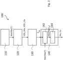
- figure 2 is then shown a flow diagram which represents an embodiment of a current sense method according to the solution here described, indicated as a whole with 100.
- Step 110 a step of performing a calibration of the ON drain to source resistance RdsONx of each external MOSFET MHx, MLx, to obtain the value of the respective drain to source resistance RdsONx as a function of temperature T, i.e., RdsONx(T).
- This step 110 may be performed preliminarily, and not all the times the method 100 is performed.
- With 140 is indicate the step of calculating the currents IHx, ILx flowing in said of each external MOSFET MHx, MLx by obtaining the respective on drain to source resistance RdsONx at the measured operating temperature T W and by obtaining said current as the ratio of the respective drain to source voltage VDS_HSx, VDS_LSx over said calculated drain to source resistance RdsONx at the operating temperature.
- the method here described in embodiments may comprises steps 120 to 140, while the calibration step 110, besides, as mentioned, being executed at a different time, e.g., at the factory, prior to the normal operation time of the circuit 10, can be possibly performed only once, e.g., at the factory, or in any case not all the times that the circuit 10 is used, i.e. the calibration 110 is performed less frequently.
- the calibration step 110 comprises in embodiments, to perform a power on, i.e., switch on, of each MOSFET MHx, MLx at an operating temperature T W corresponding to room temperature.
- a fixed calibration current Ical for example of 10A, is sent in the drain electrode of each external MOSFET MHx, MLx (and the drain to source voltage VDS_HSX, VDS_LSX must be measured by the pre-driver 12 through the amplifiers 121.
- Such fixed calibration current Ical is sent through an external current generator, not shown in the figures, in order to obtain a good accuracy.
- a curve RdsONx(T) of the variation of the on drain to source resistance RdsON as a function of the temperature is also stored in the microcontroller 111 memory, so that, as explained in the following with reference to step 140, then for each measured the drain to source voltage VDS_HSX, VDS_LSX and knowing the operating temperature T W at which the measurement is performed, the microcontroller 111 of the control module 11 is then able to calculate the current of the MOSFETs MHx, MLx.
- the step 120 of measuring the drain to source voltage of each MOSFET MHx, MLx, obtaining voltages VDS_HSx, VDS_LSx makes uses of a specific circuit arrangement in the pre-drivers stage 12 or on the same chip to measure the drain to source voltage VDS_HSx, VDS_LSx of each high and low side MOSFET MHx, MLx.
- the common node SHx signal (source of high sides MOSFETs MHx and drain of low sides MOSFETs MLx) is coupled to the multiplexer 122, through the operational amplifiers 121.
- the two amplifiers 121 x,H , 121 x,L are in amplifier operational configuration to make the read value available to the microcontroller 111 of the control logic module 11 by the two multiplexer output pins CSO1 and CSO2, one for the high side, the other for the low side, outputs of the multiplexer 122.
- Such multiplexer output pins CSO1/CSO2 are coupled to the input of an ADC, not shown, in the microcontroller 111 which reads the drain to source voltage VDS_HSx, VDS_LSx values at said pins CSO1/CSO2.
- the step 130 of measuring the operating temperature T W of said each external MOSFET MHx, MLx uses the diodes DIODE1, ..., DIODE4 controlled by the control module 11, where each diode is placed as close as possible to each respective H-bridge HB1...HB4.
- the forward voltage, Vf, of the diodes varies with temperature, therefore the temperature coefficient of the diode component embodying DIODE1, ..., DIODE4 is needed to get an accurate representation of its junction temperature.
- the control structure of the diodes DIODE1, ..., DIODE4 includes current generators 123 supplying the respective polarization currents I DIODE1 ...I DIODE4 , injecting a small polarization current (programmable from 250uA to 1mA) in the anode of the respective diode DIODE1...DIODE4, while the cathode is coupled to the ground pin GND of the pre-driver stage 12.
- each diode DIODE1, ..., DIODE4 is then measured by the analog to digital converter 123 which inputs are coupled to nodes DIODE1, ..., DIODE 4, and which digital output is coupled through a SPI Interface 112 to the microprocessor or microcontroller 111 of the control module 111.
- the forward voltage at room temperature, Vf(25°C), varies slightly from component to component: to overcome this behavior, a calibration data during the manufacturing process can be applied: in this case the forward voltage at room temperature, Vf(25°C) can be measured during the manufacturing process at the factory and the value can be stored in the microcontroller 111 memory.
- step 130 if a more precise temperature measurement is required, two methods of mapping the heat can be further adopted:
- Such measuring 130 an operating temperature T W of said one or more Field Effect Transistor MHX, MLx further comprise one or both of the following steps:
- thermal sensor or sensors represented by the diodes can also be used in the normal operation mode for controlling the maximum PCB temperature.
- the microcontroller 111 calculates the operation or working current by the following steps:
- MOSFETS arranged in H bridges, but the method here described can be applied to half bridges, and also to single external Field Effect Transistors, in particular MOSFET, representing the power driver of a load, coupled for instance to its drain.
- the solution here described refers to a method for sensing, in particular indirectly, at an electronic circuit in an integrated circuit comprising a pre-driving stage 12 driving one or more Field Effect Transistor, e.g. generically MHx, MLx, in particular MOSFET, comprised in a power stage 13 driving one or more loads, e.g. DC1...DC4, a current flowing in said one or more Field Effect Transistor, e.g. MHx, MLx, in particular MOSFET, such one or more Field Effect Transistor (MHx, MLx) being arranged external with respect to said integrated circuit in which said pre-driving stage 12 is arranged.
- MHx Field Effect Transistor
- Such one or more Field Effect Transistors can be one or more, if they are a plurality, they can be arranged in bridge configuration, e.g.,HB1...HB4, with two legs of high side and low side MOSFETS, or also in half bridges, i.e., one leg with high side and low side MOSFETs driving a load,
- half bridges such one or more external Field Effect Transistor MHx, MLx are arranged in one or more half bridge configurations each comprising a pair of high side Field Effect Transistor, e.g. MH1, MH3, MH5, MH7, and low side Field Effect Transistor, e.g. ML1, ML3, ML5, ML7,
- single amplifiers 121 coupled to their outputs, e.g. drain, may be used, which in any case perform a sampling on their output to be selected by the multiplexer 122 in order to read the drain to source voltage on the microprocessor 111.
- the solution described here is a new and innovative approach to measuring the current flowing in the external MOSFETs driven by a pre-driver on another chip.
- the proposed solution presents the advantage of not using external resistors, with the consequence of a lower cost of the application and no voltage drop in series to the load.
Landscapes
- Physics & Mathematics (AREA)
- General Physics & Mathematics (AREA)
- Engineering & Computer Science (AREA)
- Computer Hardware Design (AREA)
- Microelectronics & Electronic Packaging (AREA)
- Power Conversion In General (AREA)
- Measurement Of Current Or Voltage (AREA)
- Electronic Switches (AREA)
Abstract
said method comprising
measuring (120) a drain to source voltage (VDS_HSx, VDS_LSx), of said one or more Field Effect Transistor (MHX, MLx),
measuring (130) an operating temperature (TW) of said one or more Field Effect Transistor (MHX, MLx),
measuring (140) a current (IHX, ILx) flowing in said one or more Field Effect Transistor (MHX, MLx) by
calculating (142) the respective on drain to source resistance at the operating temperature (RdsONx(TW)) as a function (RdsONx(TW)) of said measured operating temperature (TW) and by obtaining (144) said current (IHX, ILx) as the ratio of the respective measured drain to source voltage (VDS_HSx, VDS_LSx) over said calculated drain to source resistance at the operating temperature (RdsONx(TW)).
Description
- The embodiments of the present disclosure relate to a method for sensing a current flowing in a transistor driving a load, and a corresponding circuit arrangement for sensing.
- In particular, the solutions here described are directed to sense the current flowing in the Field Effect Transistor, in particular MOSFET, at a predriving stage, the MOSFET being external with respect to the predriving stage, in the MOSFET of a H bridge driving a load, in particular a motor.
- In the state of art are known several applications which involve a pre-diver stage which controls the operation of one or more external transistors, specifically MOSFETs, which in their turn drive a load, e.g. the motor of an actuator. In particular is well to known to have MOSFETs in configuration of H bridges or half bridges to drive a load, their control signals, in particulate to their control electrode, usually the gate electrode, being supplied by a pre-driving stage.
- Here as Pre driver or predriving stage is intended an integrated circuit controlling and driving a power stage, comprising such one or more external MOSFETS, in particular in H bridge configuration, not embedded in the same integrated circuit, i.e., in the same chip. Therefore, with external MOSFET is intended a MOSFET belonging to a circuit arrangement differently packaged with respect to the pre-driving stage, i.e., on another integrated circuit or chip.
- This type of arrangement with a predriver and the power stage, i.e., the external MOSFET on different chips may occur for instance where are several actuators, using DC electric motors, for instance in the automotive field.
- In such a context, to sense and control current of the load, it is provided an operational amplifier which reads the current that flows in a series shunt resistor . Such an approach with an additional external shunt resistor, able to directly read out the current, adds however a significant cost. Moreover, in some applications, a series shunt increases the power dissipation of the system, adding a voltage drop in series with the load, which is crucial when high currents are involved.
- Considering the foregoing, an object of various embodiments of the present disclosure is to provide solutions that are able to overcome one or more of the limits of the prior art.
- According to one or more embodiments, one or more of the previous objects are achieved by a method for sensing a current and a circuit arrangement for performing the method having the distinctive elements specified in the ensuing claims. The embodiments moreover concern a corresponding method for operating such electronic architecture.
- The claims form an integral part of the technical teaching of the disclosure provided herein.
- As mentioned previously, various embodiments of the present disclosure regards a method for sensing, at an electronic circuit in an integrated circuit comprising a pre-driving stage driving one or more Field Effect Transistor, in particular MOSFET, comprised in a power stage driving one or more loads, a current flowing in said one or more Field Effect Transistor, in particular MOSFET, said one or more Field Effect Transistor being arranged external with respect to said integrated circuit in which said pre-driving stage is arranged,
- said method comprising
- measuring a drain to source voltage, of said one or more Field Effect Transistor,
- measuring an operating temperature of said one or more Field Effect Transistor,
- measuring a current flowing in said one or more Field Effect Transistor by
calculating the respective on drain to source resistance at the operating temperature as a function of said measured operating temperature and by obtaining said current as the ratio of the respective measured drain to source voltage over said calculated drain to source resistance at the operating temperature. - In various embodiments, said method further comprises calculating the respective on drain to source resistance at the operating temperature as a function of said measured operating temperature calibrated by a calibration value obtained at a given reference temperature, in particular room temperature, in particular a calibration step to obtain said calibration value being performed prior said measuring a drain to source voltage of the one or more MOSFET.
- In various embodiments, said method comprises a calibration step to obtain said calibration value comprising
- performing a power on of each Field Effect Transistor at a determined operating temperature, in particular corresponding to room temperature,
- then injecting a fixed calibration current in the drain electrode of each external Field Effect Transistor,
- measuring the corresponding drain to source voltage must be measured by the pre-driver,
- calculating the on drain to source resistance at the determined operating temperature, in particular room temperature, e.g. 25 °C, as calibration value, calculated as the ratio of the measured drain to source voltage to the fixed calibration current, storing said calibration value.
- In various embodiments, said measuring a drain to source voltage of said one or more Field Effect Transistor comprises comparing an output of of said one or more Field Effect Transistor to a respective reference voltage, in particular performing a sample and hold operation on the output of said comparison, and, in particular, selecting among the output values of the comparison of the outputs of said one or more Field Effect Transistor to a respective reference voltage the values to pass to said step of measuring a current flowing in said one or more Field Effect Transistor.
- In various embodiments, said measuring an operating temperature of said one or more Field Effect Transistor comprises measuring the forward voltage of diodes (in which is injected a determined diode current and are arranged adjacent to the one or more Field Effect Transistor so to be subject to the same operating temperature,
calculating said operating temperature as a function of a known value of the forward voltage at room temperature and of the diode forward voltage temperature coefficient, in particular the difference of the measured forward voltage to the forward voltage at room temperature over the temperature coefficient. - In various embodiments, said measuring an operating temperature of said one or more Field Effect Transistor further comprise one or both of the following steps:
- a) measuring the temperature difference between the Field Effect Transistors and the position where the corresponding diode among said diodes is soldered through a thermal map of a board on which the power stage is arranged, storing said temperature difference between the two points as a correction factor,
applying said correction factor each time said measuring an operating temperature of said one or more Field Effect Transistor is performed - b) prior performing said measuring step providing positions in said board on which the power stage is arranged where the diodes can be soldered by obtaining a heat map of said board, soldering the diodes in the points matching a difference temperature criterion, in particular showing the minimum temperature difference.
- In various embodiments, said one or more Field Effect Transistor are arranged in bridge configuration or in half bridge configuration.
- The solution described herein also refers to a circuit arrangement comprising an electronic circuit in an integrated circuit comprising a pre-driving stage driving one or more Field Effect Transistor, in particular MOSFET, comprised in a power stage driving one or more loads, a current flowing in said one or more Field Effect Transistor, in particular MOSFET, said one or more Field Effect Transistor MHx, MLx) being arranged external with respect to said integrated circuit in which said pre-driving stage is arranged, characterized in that is configured to perform the method according to any of the previous embodiments.
- In various embodiments, said electronic circuit comprises a control module comprising a microprocessor,
- said electronic circuit further comprising one or more operational differential amplifiers which inputs are coupled to the output electrode of respective among said one or more external Field Effect Transistor and the other input is coupled to the supply voltage or to ground depending if the Field Effect Transistor is coupled to the supply voltage or to ground, to output the respective drain to source voltage,
- a multiplexer receiving as input said drain to source voltages outputs of said one or more operational amplifiers and configured to select one or more of said drain to source voltages outputs as one or more of the multiplexer outputs,
- said operational differential amplifiers being configured to compare an output of of said one or more Field Effect Transistor to a respective reference voltage, in particular performing a sample and hold operation on the output of said comparison, and, in particular, selecting by said multiplexer among the output values of the comparison of the outputs of said one or more Field Effect Transistor to a respective reference voltage the values to pass to said step of measuring a current flowing in said one or more Field Effect Transistor.
- said control module then being configured, in particular by an internal analog to digital converter, to convert said one or more of said drain to source voltages in digital values supplied to said control module.
- In various embodiments, said circuit arrangement comprises one or more diodes arranged in said power stage adjacent said one or more Field Effect Transistor so that they are subject substantially to the same temperature, and said electronic circuit comprises one or more current generators controlled by said control module injecting a respective controlled current in each of said one or more diodes ,
- an analog to digital converter coupled to measure the forward voltage drop on each of said diodes and supplying its digital value to said control module.
- said circuit arrangement being configured for measuring an operating temperature of said one or more Field Effect Transistor by measuring the forward voltage of said diodes by said analog to digital converter, injecting said determined diode current by said one or more current generators,
- said control module being configured for calculating said operating temperature as a function of a known value of the forward voltage at room temperature and of the diode forward voltage temperature coefficient in particular the difference of the measured forward voltage to the forward voltage at room temperature over the temperature coefficient.
- In various embodiments, said one or more external Field Effect Transistor are arranged in one or more H-bridge configurations comprising a first pair of high side Field Effect Transistor and low side Field Effect Transistor and a second pair of high side and low side Field Effect Transistors,
- said output electrode corresponding to a node where the source of the high side Field Effect Transistor and the drain of the low side Field Effect Transistor of a pair of Field Effect Transistors are coupled,
- said one or more operational amplifiers comprising for each pair of Field Effect Transistors an amplifier coupled to said common node which other input is coupled to the source of the high side Field Effect Transistor to output the high side drain to source voltage and an amplifier coupled to said common node which other input is coupled to the drain of the low side Field Effect Transistor to output the low side drain to source voltage.
- In various embodiments, said one or more bridge configurations drive respective DC electric motors.
- The embodiments of the present disclosure will now be described with reference to the annexed drawings, which are provided purely by way of non-limiting example, and in which:
-
Figure 1 shows a schematic circuit diagram of an embodiment of a circuit arrangement according to the solution described herein; -
Figure 2 shows a flow diagram representing an embodiment of the method according to the solution described herein. - In the ensuing description, various specific details are illustrated, aimed at providing an in-depth understanding of the embodiments. The embodiments may be provided without one or more of the specific details, or with other methods, components, materials, etc. In other cases, known structures, materials, or operations are not illustrated or described in detail so that various aspects of the embodiments will not be obscured.
- Reference to "an embodiment" or "one embodiment" in the framework of the present disclosure is intended to indicate that a particular configuration, structure, or characteristic described in relation to the embodiment is comprised in at least one embodiment. Hence, phrases such as "in an embodiment" or "in one embodiment" that may be present in various points of this description do not necessarily refer to one and the same embodiment. Moreover, particular conformations, structures, or characteristics may be combined in any adequate way in one or more embodiments.
- The references used herein are provided only for convenience and hence do not define the sphere of protection or the scope of the embodiments.
- As explained previously, various embodiments of the present disclosure regard an electronic circuit arrangement comprising a predriving stage and a driving power stage comprising Field Effect transistors, in particular MOSFETs, and a method for sensing the current in such transistors.
- To this regard, in
figure 1 it is shown acircuit arrangement 10, comprising apredriving stage 12 andpower stage 13, configured to sense the current flowing in one or more, in the example a plurality, of external MOSFETS, MH1, ML1...MH8, ML8. - The
circuit arrangement 10 comprises thus anintegrated circuit predriver 12, on a respective chip, which is configured to supply driving signals IPH1, IPL1...IPH8, IPL8 tosuch power stage 13 comprising a set of one more MOSFETs, i.e., to supply them to the gate electrodes of such plurality, of external MOSFETS, MH1, ML1...MH8, ML8. Thepower stage 13 is arranged on a different or on different chips with respect to theintegrated circuit predriver 12. - A
control module 11, comprising a microprocessor or amicrocontroller 111, is shown, which is on the same chip and comprises thepredriver 12, although in variant embodiments it may be an external module with respect to thepredriver 12. - In the example of said plurality of external MOSFETS, MH1, ML1...MH8, ML8 is arranged in a plurality of half bridges, HB1...HB8, which drive corresponding motors DC1...DC7 .
- With x=1, 2,..., 8 is here indicated the index of a generic leg of the half bridge HBx, comprising MOSFET MHx, MLx. In general, a H-bridge comprises two legs each including two MOSFETS in series arranged between the voltage supply VDH and the ground GND. In example of
Figure 1 , half bridges using each a single leg are used. The generic high side MOSFET, here indicate with MHx, of the x-th leg has its drain coupled to the voltage supply VDH, while the low side MOSFET, MHx, has its source coupled to ground GND. The source of the high side MOSFET MHx and the drain of the low side MOSFET MLx, which are their output electrodes, are coupled together in a common output node SHx which is the output of the leg and in the example shown it is coupled to one of the terminals of the respective motor. In the example shown, there is a first leg, MH1, ML1 with an output node SH1 coupled to a terminal of a first motor DC1, then a second leg MH2, ML2, coupled to the other terminal of the first motor DC1 by its output node SH2. Such legs MH1, ML1 and MH2, ML2 form the first half bridge HB1. The second leg MH2, ML2 of the first bridge HB1 is also coupled to a terminal of the second motor DC2, by its output node SH2, then a third leg MH3, ML3, is coupled to the other terminal of the second motor DC2 by its output node SH3. Proceeding accordingly seven motors DC1...DC7 can be driven using eight half bridges HB1...HB8. - The gate electrodes of the MOSFETS MHx, MLx of a generic leg of one of the half bridges HB1...HB8 are driven by driving signals, high side driving signal IPHx and low side driving signal IPLx, that command their open and close state according to configurations which are known per se in the art of driving half bridges and full H-bridges and determine for instance the corresponding motor to move right or left, or coast, or brake, or go in short circuit state.
- In
figure 1 are also indicated on their source electrodes the currents IHx, ILx flowing in said of each external MOSFET MHx, MLx, which are to be sensed in order to obtain a control quantity which can be used by thecontrol module 11 to control the driving of the MOSFET MHx, MLx by thepre-driver stage 12. - In the
circuit arrangement 10 the output nodes SHx are coupled to the input of operational amplifiers 121 in thepredriver 12. As shown, each output node SHx is coupled to the inverting input terminal of a high side operational amplifier 121x,H, which other input terminal is coupled also high side, i.e. to the voltage supply VDH, while the output node SHx is also coupled to the positive input of another operational amplifier 121x, L, which other input terminal is coupled low side, to the ground GND. - Therefore the high side operational amplifier 121x,H amplifies the difference of the source voltage of the high side MOSFET to the voltage supply VDH, which corresponds to the drain voltage of the high side MOSFET, MHx, i.e., outputs a high side drain to source voltage VDS_HSX, while the other low side operational amplifier 121x,L correspondingly obtains the low side drain to source voltage VDS_LSX, this time amplifying the difference of the drain voltage of the low side MOSFET MLx to the ground voltage GND. Of course, the operational amplifiers 121 may have one as amplifying ratio, although other value of gain can be of course managed, e.g., by the control module.
- A
multiplexer 122 receives the high side and low side drain to source voltages outputted by the operational differential amplifiers 121, which preferably are in sample and hold configuration, and under the control a selection signal issued for instance by the control module can select on outputs CSO1, CSO2 which are supplied to the control module (i.e., to the microprocessor or microcontroller 111). - Diodes DIODE1, ...DIODE4 are arranged in proximity with the MOSFETS of each pair of bridges HB1...HB8, so that they are subject to the same operating temperature or working temperature. With same operating temperature of course is here is meant a temperature very close, ideally the same, or with a small difference, the operating temperature, same or with a small difference, of the diode varying substantially as the temperature of the MOSFETs or JFET to which are adjacent. In their anodes are injected respective polarization currents IDIODE1, IDIODE4 by respective
current generators 1231...1234, which are shown as comprised in thepredriver 12. - In particular, in the embodiment shown, since there are four diodes DIODE1, ...DIODE4, and eight legs HB1...HB8, it is chosen to place the diode near the high side MOSFET which while driving a motor, e.g. DC1, is conducting the most of time. With two half bridges, such as HB1 and HB2, coupled to the terminals of the motor DC1, they are usually driven, in order in order to have the motor rotate in the forward direction, by maintaining the high side MOSFET MH1 of the first leg HB1 switched on and by using the state of switch on and switch off of the low side MOSFET ML2 of the other leg HB2 to control the motor. Therefore, diode DIODE1 is placed closed to the high side MOSFET MH1. The other diodes are placed with the same criterion. This allows to use only four diodes and a corresponding number of
current generators 1231,..., 1234, in order to limit the size of the whole circuit and of the chip, as well as the costs. Clearly, if the size or the costs of the circuit and chip allow, in variant embodiment each high side MOSFET may have a diode place nearby, and in general different number of diodes and placements may be use depending on the circuit parameters and requirements. - The
predriver stage 12 includes an analog todigital converter 123 which inputs are coupled to the anodes of diodes DIODE1,..., DIODE4, and which digital output is coupled through aSPI Interface 112 to the microprocessor ormicrocontroller 11 of thecontrol module 11. - In
figure 2 is then shown a flow diagram which represents an embodiment of a current sense method according to the solution here described, indicated as a whole with 100. - With 110 is indicated a step of performing a calibration of the ON drain to source resistance RdsONx of each external MOSFET MHx, MLx, to obtain the value of the respective drain to source resistance RdsONx as a function of temperature T, i.e., RdsONx(T). This
step 110 may be performed preliminarily, and not all the times themethod 100 is performed. - With 120 is indicated a step of measuring the drain to source voltage of each external MOSFET MHx, MLx, obtaining respective voltages VDS_HSX VDS_LSX.
- With 130 is indicated a subsequent step of measuring the operating temperature TW of said of each external MOSFET MHx, MLx.
- With 140 is indicate the step of calculating the currents IHx, ILx flowing in said of each external MOSFET MHx, MLx by obtaining the respective on drain to source resistance RdsONx at the measured operating temperature TW and by obtaining said current as the ratio of the respective drain to source voltage VDS_HSx, VDS_LSx over said calculated drain to source resistance RdsONx at the operating temperature.
- The method here described in embodiments may comprises
steps 120 to 140, while thecalibration step 110, besides, as mentioned, being executed at a different time, e.g., at the factory, prior to the normal operation time of thecircuit 10, can be possibly performed only once, e.g., at the factory, or in any case not all the times that thecircuit 10 is used, i.e. thecalibration 110 is performed less frequently. - The
calibration step 110 comprises in embodiments, to perform a power on, i.e., switch on, of each MOSFET MHx, MLx at an operating temperature TW corresponding to room temperature. - Then a fixed calibration current Ical, for example of 10A, is sent in the drain electrode of each external MOSFET MHx, MLx (and the drain to source voltage VDS_HSX, VDS_LSX must be measured by the pre-driver 12 through the amplifiers 121. Such fixed calibration current Ical is sent through an external current generator, not shown in the figures, in order to obtain a good accuracy.
- The
logic module 11, e.g., themicrocontroller 111, then calculates the on drain to source resistance RdsON at room temperature, e.g., 25 °C, as the ratio of the drain to source voltage to the fixed current, i.e., e.g., VDS_HSX/10A for the high side. This value is stored in thelogic module 11, e.g., in themicrocontroller 11 memory. - A curve RdsONx(T) of the variation of the on drain to source resistance RdsON as a function of the temperature is also stored in the
microcontroller 111 memory, so that, as explained in the following with reference to step 140, then for each measured the drain to source voltage VDS_HSX, VDS_LSX and knowing the operating temperature TW at which the measurement is performed, themicrocontroller 111 of thecontrol module 11 is then able to calculate the current of the MOSFETs MHx, MLx. - The
step 120 of measuring the drain to source voltage of each MOSFET MHx, MLx, obtaining voltages VDS_HSx, VDS_LSx makes uses of a specific circuit arrangement in thepre-drivers stage 12 or on the same chip to measure the drain to source voltage VDS_HSx, VDS_LSx of each high and low side MOSFET MHx, MLx. - Such circuit arrangement does not require external pins, i.e., external with respect to the chip of the pre-driver 12: the common node SHx signal (source of high sides MOSFETs MHx and drain of low sides MOSFETs MLx) is coupled to the
multiplexer 122, through the operational amplifiers 121. - When the drain to source voltage VDS_HSx of the generic high side MOSFET MHx is required, the voltage on the respective output common mode SHx is brought to the common input of the two dedicated amplifiers 121x,H, 121x,L.
- The two amplifiers 121x,H, 121x,L are in amplifier operational configuration to make the read value available to the
microcontroller 111 of thecontrol logic module 11 by the two multiplexer output pins CSO1 and CSO2, one for the high side, the other for the low side, outputs of themultiplexer 122. Such multiplexer output pins CSO1/CSO2 are coupled to the input of an ADC, not shown, in themicrocontroller 111 which reads the drain to source voltage VDS_HSx, VDS_LSx values at said pins CSO1/CSO2. - The
step 130 of measuring the operating temperature TW of said each external MOSFET MHx, MLx uses the diodes DIODE1, ..., DIODE4 controlled by thecontrol module 11, where each diode is placed as close as possible to each respective H-bridge HB1...HB4. The forward voltage, Vf, of the diodes varies with temperature, therefore the temperature coefficient of the diode component embodying DIODE1, ..., DIODE4 is needed to get an accurate representation of its junction temperature. The control structure of the diodes DIODE1, ..., DIODE4 includescurrent generators 123 supplying the respective polarization currents IDIODE1...IDIODE4, injecting a small polarization current (programmable from 250uA to 1mA) in the anode of the respective diode DIODE1...DIODE4, while the cathode is coupled to the ground pin GND of thepre-driver stage 12. - The voltage drop across each diode DIODE1, ..., DIODE4 is then measured by the analog to
digital converter 123 which inputs are coupled to nodes DIODE1, ..., DIODE 4, and which digital output is coupled through aSPI Interface 112 to the microprocessor ormicrocontroller 111 of thecontrol module 111. - By reading the forward voltage at an unknown temperature Y, Vf(Y°C), knowing the forward voltage at room temperature, Vf(25°C), in particular at 25°C and knowing the temperature coefficient TC of the forward voltage Vf, the
microcontroller 111 calculates the operating or working temperature TW[°C] by applying the following formula:
- The forward voltage at room temperature, Vf(25°C), varies slightly from component to component: to overcome this behavior, a calibration data during the manufacturing process can be applied: in this case the forward voltage at room temperature, Vf(25°C) can be measured during the manufacturing process at the factory and the value can be stored in the
microcontroller 111 memory. - Regarding
step 130, if a more precise temperature measurement is required, two methods of mapping the heat can be further adopted: - a) the first method provides measuring the temperature difference between the H-bridge MOSFETs MHx, MLx and the point where the corresponding diode among diodes DIODE1...DIODE4 is soldered through the thermal map of the application board. The temperature difference between the two points is then saved in the memory of the
microcontroller 111 as a correction factor: each time themicrocontroller 111 carries out the temperature measurement in thestep 130 through the corresponding diode among diodes DIODE1...DIODE4, themicrocontroller 111 applies such previously stored correction factor to obtain a temperature measurement of the MOSFET MHx, MLx which is closer to reality. - b) the second method provides places in the PCB (Printed Circuit Board) where the diodes DIODE1, ..., DIODE4 can be soldered in order to find the best spot to sense the temperature. By obtaining a heat map of the application board the user is able to discover the most suitable place where to put the thermal sensor. In this way the measurement made by the selected diode among diodes DIODE1...DIODE4 is closer to the real MOSFET temperature. In any case, a corrective factor, as provided by the solution a) can be taken into consideration.
- Thus, such measuring 130 an operating temperature TW of said one or more Field Effect Transistor MHX, MLx further comprise one or both of the following steps:
- a) measuring the temperature difference between the Field Effect Transistors MHx, MLx and the position where the corresponding diode among said diodes DIODE1...DIODE4 is soldered through a thermal map of a board on which the
power stage 13 is arranged, storing said temperature difference between the two points as a correction factor,
applying said correction factor each time said measuring 130 an operating temperature TW of said one or more Field Effect Transistor MHX, MLx is performed - b) prior performing said measuring
step 130 providing positions in said board on which thepower stage 13 is arranged where the diodes DIODE1, ..., DIODE4 can be soldered by obtaining a heat map of said board, soldering the diodes DIODE1, ..., DIODE4 in the points matching a difference temperature criterion, in particular showing the minimum temperature difference. - It is underlined the thermal sensor or sensors represented by the diodes can also be used in the normal operation mode for controlling the maximum PCB temperature.
- Then, regarding the
step 140 of measuring the current flowing in said of each external MOSFET MHx, MLx, after having known the temperature at which the corresponding H-bridge is working fromstep 130 and having measured the drain to source voltage VDS_HSx, VDS_LSx, themicrocontroller 111 calculates the operation or working current by the following steps: - calculating 142 the RdsON at working temperature, RdsONx(TW). The
microcontroller 111 has in its memory the trend of the variation curve RdsON(T) in temperature: knowing the temperature, themicrocontroller 11 can estimate the value of the on drain to source resistance RdsONx(TW) at the operating temperature TW at which the H bridge corresponding to MOSFET MHx, MLx is working; - then calculating 144 the current IHx, ILx, flowing through the external MOSFETS MOSFET MHx, MLx. At this point, for instance for the high side MOSFET MHx (for the low side MOSFET the calculation is dual) the
microcontroller 111 has calculated the value of the on drain to source resistance RdsONx(TW) at the operating temperature TW and has acquired the measured value of the drain to source voltage VDS_HSx of the higher side MOSFET MHx: the current IHx flowing in the H-bridge is calculated as the ratio between the drain to source voltage VDS_HSx VDS_HSx and the drain to source resistance RdsONx(TW) at the operating temperature TW. - By way of example:
- in step 110 a calibration current Ical = 10 A ± 1% is applied which gives a calibration drain to source voltage Vds_cal = 0.7 V ± 0.002V. Thus, their ratio is Rds ON_cal = 70 mS2 ± 1% @25C = RDsONx (25°C) ;
- then the
step 130 of measurement of the temperature measures or reads the room temperature forward voltage of the diode Vf(25°C) = 0.6 V ± 0.005 V, while during operation of thecircuit 10 is measured Vf (TW) = 0.4 V ± 0.005 V. The operating temperature TW is thus obtained as 125 °C ± 5% from the Vf(T) curve stored in themicrocontroller 111; - subsequently, using the temperature curve of the on drain source resistance RdsON stored in the
microcontroller 111, instep 142 is RdsONx(T) = RDsONx(25°C)*[1+(Tw-25)/150] = 116 mΩ ± 6%. 1*[1+(Tw-Ta(=25°C)/150] is the formula of the curve of the RdsONx(T), with Ta room temperature; - then, as for
step 130, VDS = 1V ± 0.002V => 1V ± ≈ 0%, VDS can be VDS_HSx or VDS_LSx; - in the
step 144 it is calculated I = Vds/Rds(on) (T) = 8.6 A ± 6%, I can be IHx or ILx. - It is underlined that the description is referred to MOSFETS arranged in H bridges, but the method here described can be applied to half bridges, and also to single external Field Effect Transistors, in particular MOSFET, representing the power driver of a load, coupled for instance to its drain.
- Thus in general the solution here described refers to a method for sensing, in particular indirectly, at an electronic circuit in an integrated circuit comprising a
pre-driving stage 12 driving one or more Field Effect Transistor, e.g. generically MHx, MLx, in particular MOSFET, comprised in apower stage 13 driving one or more loads, e.g. DC1...DC4, a current flowing in said one or more Field Effect Transistor, e.g. MHx, MLx, in particular MOSFET, such one or more Field Effect Transistor (MHx, MLx) being arranged external with respect to said integrated circuit in which saidpre-driving stage 12 is arranged. Such one or more Field Effect Transistors, specifically MOSFETS can be one or more, if they are a plurality, they can be arranged in bridge configuration, e.g.,HB1...HB4, with two legs of high side and low side MOSFETS, or also in half bridges, i.e., one leg with high side and low side MOSFETs driving a load, - the
method 100 comprising - measuring, step 120 a drain to source voltage VDS_HSx, VDS_LSx, of said one or more Field Effect Transistor MHX, MLx,
- measuring,
step 130, an operating temperature, TW of said one or more Field Effect Transistor, MHX, MLx, - measuring, step 140 a current IHX, ILx flowing in said one or more Field Effect Transistor (MHX, MLx), i.e. the current flowing from drain to source, by
calculating,step 142, the respective on drain to source resistance at the operating temperature, e.g. RdsONx(TW)) as a function, e.g. the stored curve (RdsONx(T)) or a stored equation describing the variation of the RdsON with the temperature T, of said measured operating temperature, e.g. TW, and by obtaining,step 144, said current, IHX, ILx, as the ratio of the respective measured drain to source voltage VDS_HSx, VDS_LSx over such calculated drain to source resistance at the operating temperature, e.g. RdsONx(TW). - If half bridges are used, such one or more external Field Effect Transistor MHx, MLx are arranged in one or more half bridge configurations each comprising a pair of high side Field Effect Transistor, e.g. MH1, MH3, MH5, MH7, and low side Field Effect Transistor, e.g. ML1, ML3, ML5, ML7,
- the output electrode corresponding to a node, e.g. generically SHx, where the source of the high side Field Effect Transistor, e.g. MH1, MH3, MH5, MH7, and the drain of the low side Field Effect Transistor (e.g. ML1, ML3, ML5, ML7 of a pair of Field Effect Transistors, in this case the first pair, are coupled,
- the one or more operational amplifiers 121 comprising for each pair of Field Effect Transistors, generically MHx, MLx an amplifier 121H,x coupled to such common node SHx, which other input is coupled to the source of the high side Field Effect Transistor MH1, MH3, MH5, MH7, to output the high side drain to source voltage, VDS_HSx, and an amplifier, 121L,x, coupled to said common node SHx, which other input is coupled to the drain of the low side Field Effect Transistor, ML1, ML3, ML5, ML7, to output the low side drain to source voltage, VDS_LSx.
- In case, full H-bridges, with two legs each, are used to drive the load, at each common node of a leg, i.e. pair of high side and low side Field Effect Transistor, a respective pair of amplifiers 121x,H, 121x,L is coupled.
- In case single FET or MOSFETs are used, not bridges, to drive a load, single amplifiers 121 coupled to their outputs, e.g. drain, may be used, which in any case perform a sampling on their output to be selected by the
multiplexer 122 in order to read the drain to source voltage on themicroprocessor 111. - Thus, based on the above, the advantages of the described solution are clear.
- The solution described here is a new and innovative approach to measuring the current flowing in the external MOSFETs driven by a pre-driver on another chip. The proposed solution presents the advantage of not using external resistors, with the consequence of a lower cost of the application and no voltage drop in series to the load.
- The removal from an application board of the sensing resistors is possible, which have a significant cost in the total budget of the full application.
- Of course, without prejudice to the principle of the invention, the details of construction and the embodiments may vary widely with respect to what has been described and illustrated herein purely by way of example, without thereby departing from the scope of the present invention, as defined by the ensuing claims.
- The description above is referred to Field Effect Transistors which are embodied by MOSFETs, although the solution may encompass other types of Field Effect Transistors, such as JFET.
Claims (13)
- A method for sensing, at an electronic circuit in an integrated circuit comprising a pre-driving stage (12) driving one or more Field Effect Transistor (MHx, MLx), in particular MOSFET, comprised in a power stage (13) driving one or more loads (DC1...DC4), a current flowing in said one or more Field Effect Transistor (MHx, MLx), in particular MOSFET, said one or more Field Effect Transistor (MHx, MLx) being arranged external with respect to said integrated circuit in which said pre-driving stage (12) is arranged,said method (100) comprisingmeasuring (120) a drain to source voltage (VDS_HSx, VDS_LSx), of said one or more Field Effect Transistor (MHX, MLx),measuring (130) an operating temperature (TW) of said one or more Field Effect Transistor (MHX, MLx),measuring (140) a current (IHX, ILx) flowing in said one or more Field Effect Transistor (MHX, MLx) by
calculating (142) the respective on drain to source resistance at the operating temperature (RdsONx(TW)) as a function (RdsONx(TW)) of said measured operating temperature (TW) and by obtaining (144) said current (IHX, ILx) as the ratio of the respective measured drain to source voltage (VDS_HSx, VDS_LSx) over said calculated drain to source resistance at the operating temperature (RdsONx(TW)) . - A method according to claim 1, wherein said method further comprises calculating (142) the respective on drain to source resistance at the operating temperature (RdsONx(TW)) as a function of said measured operating temperature (TW) calibrated by a calibration value (RdsONx(25°C)) obtained at a given reference temperature (Ta, 25°C), in particular room temperature, in particular a calibration step (110) to obtain said calibration value (RdsONx(25°C)) being performed prior said measuring (120) a drain to source voltage (VDS_HSx, VDS_LSx) of the one or more MOSFET (MHx, MLx).
- A method according to claim 1 or 2, wherein said method comprises a calibration step (110) to obtain said calibration value (RdsONx(25°C)) comprisingperforming a power on of each Field Effect Transistor (MHx, MLx) at a determined operating temperature (TW), in particular corresponding to room temperature,then injecting a fixed calibration current (Ical) in the drain electrode of each external Field Effect Transistor (MHx, MLx),measuring the corresponding drain to source voltage (VDS_HSX, VDS_LSX) must be measured by the pre-driver 12,calculating the on drain to source resistance at the determined operating temperature (TW), in particular room temperature, e.g. 25 °C, as calibration value, calculated as the ratio of the measured drain to source voltage (VDS_HSX, VDS_LSX) to the fixed calibration current (Ical), storing said calibration value (RdsONx(25°C) .
- A method according to any of claims 1 to 3, wherein said measuring (120) a drain to source voltage (VDS_HSx, VDS_LSx) of said one or more Field Effect Transistor (MHX, MLx) comprises comparing an output (SHx) of of said one or more Field Effect Transistor (MHX, MLx) to a respective reference voltage (VDH, GND), in particular performing a sample and hold operation on the output of said comparison, and, in particular, selecting (122) among the output values of the comparison of the outputs (SHx) of said one or more Field Effect Transistor (MHX, MLx) to a respective reference voltage (VDH, GND) the values to pass to said step of measuring (140) a current (IHX, ILx) flowing in said one or more Field Effect Transistor (MHX, MLx).
- A method according to any of claims 1 to 4, wherein said measuring (130) an operating temperature (TW) of said one or more Field Effect Transistor (MHX, MLx) comprises measuring the forward voltage (Vf) of diodes (DIODE1, ..., DIODE4) in which is injected a determined diode current (IDIODE1,... ,IDIODE4) and are arranged adjacent to the one or more Field Effect Transistor (MHX, MLx) so to be subject to a same operating temperature (TW),
calculating said operating temperature (TW) as a function of a known value of the forward voltage at room temperature (Vf(25°C)) and of the diode forward voltage temperature coefficient TC, in particular the difference of the measured forward voltage to the forward voltage at room temperature (Vf(25°C)) over the temperature coefficient (TC). - A method according to claim 5, wherein said measuring (130) an operating temperature (TW) of said one or more Field Effect Transistor (MHX, MLx) further comprise one or both of the following steps:a) measuring the temperature difference between the Field Effect Transistors (MHx, MLx) and the position where the corresponding diode among said diodes (DIODE1...DIODE4) is soldered through a thermal map of a board on which the power stage (13) is arranged, storing said temperature difference between the two points as a correction factor,
applying said correction factor each time said measuring (130) an operating temperature (TW) of said one or more Field Effect Transistor (MHX, MLx) is performedb) prior performing said measuring step (130) providing positions in said board on which the power stage (13) is arranged where the diodes (DIODE1, ..., DIODE4) can be soldered by obtaining a heat map of said board, soldering the diodes (DIODE1, ..., DIODE4) in the points matching a difference temperature criterion, in particular showing the minimum temperature difference. - A method according to any of claims 1 to 6, wherein said one or more Field Effect Transistor (MHX, MLx) are arranged in a full H-bridge configuration or in a half bridge configuration (HB1...HB8).
- A circuit arrangement (10) comprising an electronic circuit (11) in an integrated circuit comprising a pre-driving stage (12) driving one or more Field Effect Transistor (MHx, MLx), in particular MOSFET, comprised in a power stage (13) driving one or more loads (DC1...DC4), a current flowing in said one or more Field Effect Transistor (MHx, MLx), in particular MOSFET, said one or more Field Effect Transistor MHx, MLx) being arranged external with respect to said integrated circuit in which said pre-driving stage (12) is arranged, characterized in that is configured to perform the method according to any of claims 1 to 7.
- A circuit according to claim 8, whereinsaid electronic circuit comprises a control module (11) comprising a microprocessor (111),said electronic circuit further comprising one or more operational differential amplifiers (121) which inputs are coupled to the output electrode (SHx) of respective among said one or more external Field Effect Transistor (MHx, MLx) and the other input is coupled to the supply voltage (VDD) or to ground (GDD) depending if the Field Effect Transistor is coupled to the supply voltage (VDD) or to ground (GND), to output the respective drain to source voltage,a multiplexer (122) receiving as input said drain to source voltages outputs (VDS_HSx, VDS_LSx) of said one or more operational amplifiers (121) and configured to select one or more of said drain to source voltages outputs (VDS_HSx, VDS_LSx) as one or more of the multiplexer outputs,said operational differential amplifiers (121) being configured to compare an output (SHx) of of said one or more Field Effect Transistor (MHX, MLx) to a respective reference voltage (VDH, GND), in particular performing a sample and hold operation on the output of said comparison, and, in particular, selecting (122) by said multiplexer among the output values of the comparison of the outputs (SHx) of said one or more Field Effect Transistor (MHX, MLx) to a respective reference voltage (VDH, GND) the values to pass to said step of measuring (140) a current (IHX, ILx) flowing in said one or more Field Effect Transistor (MHX, MLx).said control module (11) then being configured, in particular by an internal analog to digital converter, to convert said one or more of said drain to source voltages (VDS_HSx, VDS_LSx) in digital values supplied to said control module (11).
- A circuit according to claim 8 or 9, wherein said circuit arrangement comprises one or more diodes (DIODE1...DIODE4) arranged in said power stage (13) adjacent said one or more Field Effect Transistor (MHx, MLx) so that they are subject substantially to the same temperature, and said electronic circuit comprises one or more current generators (124) controlled by said control module (11) injecting a respective controlled current (IDIODE1,..., IDIODE4) in each of said one or more diodes (DIODE1...DIODE4),
an analog to digital converter (123) coupled to measure the forward voltage (Vf) drop on each of said diodes (DIODE1...DIODE4) and supplying its digital value to said control module (11). - A circuit according to any of claims 8 to 10, wherein said circuit arrangement being configured for measuring (130) an operating temperature (TW) of said one or more Field Effect Transistor (MHX, MLx) by measuring the forward voltage (Vf) of said diodes (DIODE1, ..., DIODE4) by said analog to digital converter (123), injecting said determined diode current (IDIODE1,... ,IDIODE4) by said one or more current generators (124),
said control module (11) being configured for calculating said operating temperature (TW) as a function of a known value of the forward voltage at room temperature (Vf(25°C)) and of the diode forward voltage temperature coefficient TC, in particular the difference of the measured forward voltage to the forward voltage at room temperature (Vf(25°C)) over the temperature coefficient (TC). - A circuit according to any of claims 8 to 11, wherein said one or more external Field Effect Transistor (MHx, MLx) are arranged in one or more half bridge configurations (HB1,..., HB8) comprising each a pair of high side Field Effect Transistor (MH1, MH3, MH5, MH7) and low side Field Effect Transistor (ML1, ML3, ML5, ML7),said output electrode corresponding to a node (SHx) where the source of the high side Field Effect Transistor (MH1, MH3, MH5, MH7) and the drain of the low side Field Effect Transistor (ML1, ML3, ML5, ML7) of a pair of Field Effect Transistors are coupled,said one or more operational amplifiers (121) comprising for each pair of Field Effect Transistors (MHx, MLx) an amplifier (121H,x) coupled to said common node (SHx) which other input is coupled to the source of the high side Field Effect Transistor (MH1, MH3, MH5, MH7) to output the high side drain to source voltage (VDS_HSx) and an amplifier (121L,x) coupled to said common node (SHx) which other input is coupled to the drain of the low side Field Effect Transistor (ML1, ML3, ML5, ML7) to output the low side drain to source voltage (VDS_LSx).
- A circuit according to any of claims 8 to 11, wherein said one or more bridge configurations drive respective DC electric motors (DC1...DC7).
Applications Claiming Priority (1)
| Application Number | Priority Date | Filing Date | Title |
|---|---|---|---|
| IT102022000019947A IT202200019947A1 (en) | 2022-09-28 | 2022-09-28 | PROCEDURE FOR DETECTING A CURRENT FLOWING IN A TRANSISTOR DRIVING A LOAD, AND CORRESPONDING CIRCUIT ARRANGEMENT FOR THE DETECTION |
Publications (1)
| Publication Number | Publication Date |
|---|---|
| EP4345464A1 true EP4345464A1 (en) | 2024-04-03 |
Family
ID=84369590
Family Applications (1)
| Application Number | Title | Priority Date | Filing Date |
|---|---|---|---|
| EP23196500.5A Pending EP4345464A1 (en) | 2022-09-28 | 2023-09-11 | A method for sensing a current flowing in a transistor driving a load, and a corresponding circuit arrangement for sensing |
Country Status (4)
| Country | Link |
|---|---|
| US (1) | US12523681B2 (en) |
| EP (1) | EP4345464A1 (en) |
| CN (1) | CN117792375A (en) |
| IT (1) | IT202200019947A1 (en) |
Citations (3)
| Publication number | Priority date | Publication date | Assignee | Title |
|---|---|---|---|---|
| US5959464A (en) * | 1996-09-03 | 1999-09-28 | Motorola Inc. | Loss-less load current sensing driver and method therefor |
| US9831773B2 (en) * | 2015-12-18 | 2017-11-28 | Infineon Technologies Americas Corp. | Current sensing in a power supply |
| CN113030683A (en) * | 2021-03-15 | 2021-06-25 | 五羊—本田摩托(广州)有限公司 | Method, medium and computer equipment for measuring temperature of power switch device |
Family Cites Families (4)
| Publication number | Priority date | Publication date | Assignee | Title |
|---|---|---|---|---|
| EP2846464B1 (en) * | 2012-05-01 | 2019-01-09 | Shunzou Ohshima | Overcurrent protection power supply apparatus |
| WO2016077970A1 (en) * | 2014-11-17 | 2016-05-26 | Micron Technology, Inc. | Apparatuses and methods for compensating for process, voltage, and temperature variation in a memory |
| JP6953512B2 (en) * | 2016-08-08 | 2021-10-27 | パワー・インテグレーションズ・インコーポレーテッド | Integrated circuits for high-speed temperature detection of semiconductor switching devices |
| US10707767B2 (en) * | 2018-12-04 | 2020-07-07 | Infineon Technologies Austria Ag | Two-level switch driver for preventing avalanche breakdown for a synchronous rectification switch in a power converter operating in a low-power burst mode |
-
2022
- 2022-09-28 IT IT102022000019947A patent/IT202200019947A1/en unknown
-
2023
- 2023-09-11 EP EP23196500.5A patent/EP4345464A1/en active Pending
- 2023-09-21 US US18/371,313 patent/US12523681B2/en active Active
- 2023-09-27 CN CN202311260729.8A patent/CN117792375A/en active Pending
Patent Citations (3)
| Publication number | Priority date | Publication date | Assignee | Title |
|---|---|---|---|---|
| US5959464A (en) * | 1996-09-03 | 1999-09-28 | Motorola Inc. | Loss-less load current sensing driver and method therefor |
| US9831773B2 (en) * | 2015-12-18 | 2017-11-28 | Infineon Technologies Americas Corp. | Current sensing in a power supply |
| CN113030683A (en) * | 2021-03-15 | 2021-06-25 | 五羊—本田摩托(广州)有限公司 | Method, medium and computer equipment for measuring temperature of power switch device |
Also Published As
| Publication number | Publication date |
|---|---|
| US12523681B2 (en) | 2026-01-13 |
| US20240103046A1 (en) | 2024-03-28 |
| CN117792375A (en) | 2024-03-29 |
| IT202200019947A1 (en) | 2024-03-28 |
Similar Documents
| Publication | Publication Date | Title |
|---|---|---|
| US10381913B2 (en) | Power supply control device and control characteristic correction data generation method for power supply control device | |
| US20110234189A1 (en) | Current control device for electric load | |
| US10018658B2 (en) | Class D audio amplifier and method for reading a current supplied by the amplifier | |
| WO2021240891A1 (en) | Power conversion device | |
| JP2016200570A (en) | Semiconductor device current detection method and semiconductor device | |
| CN103852706B (en) | Consider determine the barrier layer temperature of power semiconductor method and its realization device with degenerating | |
| US7202711B2 (en) | Technique for determining a load current | |
| CN103477234A (en) | Current sensor | |
| US20040159489A1 (en) | Control unit for electric power steering | |
| US20130049779A1 (en) | Integrated circuit | |
| CN101189796A (en) | Circuit and method for determining load current | |
| CN116260335A (en) | Power modules and DC-DC converters | |
| US20150346312A1 (en) | Method for setting up a current sensor | |
| JPH06281693A (en) | Method for measuring thermal resistance of semiconductor device | |
| US7363186B1 (en) | Apparatus and method for self calibration of current feedback | |
| US12523681B2 (en) | Transistor driving a load, and corresponding circuit arrangement for sensing | |
| JP2012109659A (en) | Load drive circuit | |
| JP2012054804A (en) | Protection device for load driving circuit | |
| US20200236823A1 (en) | Multi-die temperature control device and method for controlling temperature of multi-die power module | |
| JP2013513119A (en) | Method and apparatus for calibrating voltage measurements in a driver circuit | |
| US6856147B2 (en) | Resistive load measurement system | |
| JP4654765B2 (en) | Load driving device and output adjusting method of load driving device | |
| CN117220560A (en) | Inverter for thermal protection and method for measuring junction temperature | |
| JP3084857B2 (en) | Method for measuring thermal resistance of power semiconductor device | |
| JP3649082B2 (en) | Operational amplifier measuring circuit and measuring method thereof |
Legal Events
| Date | Code | Title | Description |
|---|---|---|---|
| PUAI | Public reference made under article 153(3) epc to a published international application that has entered the european phase |
Free format text: ORIGINAL CODE: 0009012 |
|
| STAA | Information on the status of an ep patent application or granted ep patent |
Free format text: STATUS: THE APPLICATION HAS BEEN PUBLISHED |
|
| AK | Designated contracting states |
Kind code of ref document: A1 Designated state(s): AL AT BE BG CH CY CZ DE DK EE ES FI FR GB GR HR HU IE IS IT LI LT LU LV MC ME MK MT NL NO PL PT RO RS SE SI SK SM TR |
|
| STAA | Information on the status of an ep patent application or granted ep patent |
Free format text: STATUS: REQUEST FOR EXAMINATION WAS MADE |
|
| 17P | Request for examination filed |
Effective date: 20241001 |
|
| RBV | Designated contracting states (corrected) |
Designated state(s): AL AT BE BG CH CY CZ DE DK EE ES FI FR GB GR HR HU IE IS IT LI LT LU LV MC ME MK MT NL NO PL PT RO RS SE SI SK SM TR |
|
| STAA | Information on the status of an ep patent application or granted ep patent |
Free format text: STATUS: EXAMINATION IS IN PROGRESS |
|
| 17Q | First examination report despatched |
Effective date: 20260121 |