EP4344038A1 - Llc converter with synchronous rectification - Google Patents
Llc converter with synchronous rectification Download PDFInfo
- Publication number
- EP4344038A1 EP4344038A1 EP22197056.9A EP22197056A EP4344038A1 EP 4344038 A1 EP4344038 A1 EP 4344038A1 EP 22197056 A EP22197056 A EP 22197056A EP 4344038 A1 EP4344038 A1 EP 4344038A1
- Authority
- EP
- European Patent Office
- Prior art keywords
- switches
- llc converter
- control unit
- bridge
- primary side
- Prior art date
- Legal status (The legal status is an assumption and is not a legal conclusion. Google has not performed a legal analysis and makes no representation as to the accuracy of the status listed.)
- Pending
Links
Images


Classifications
-
- H—ELECTRICITY
- H02—GENERATION; CONVERSION OR DISTRIBUTION OF ELECTRIC POWER
- H02M—APPARATUS FOR CONVERSION BETWEEN AC AND AC, BETWEEN AC AND DC, OR BETWEEN DC AND DC, AND FOR USE WITH MAINS OR SIMILAR POWER SUPPLY SYSTEMS; CONVERSION OF DC OR AC INPUT POWER INTO SURGE OUTPUT POWER; CONTROL OR REGULATION THEREOF
- H02M3/00—Conversion of DC power input into DC power output
- H02M3/01—Resonant DC/DC converters
-
- H—ELECTRICITY
- H02—GENERATION; CONVERSION OR DISTRIBUTION OF ELECTRIC POWER
- H02M—APPARATUS FOR CONVERSION BETWEEN AC AND AC, BETWEEN AC AND DC, OR BETWEEN DC AND DC, AND FOR USE WITH MAINS OR SIMILAR POWER SUPPLY SYSTEMS; CONVERSION OF DC OR AC INPUT POWER INTO SURGE OUTPUT POWER; CONTROL OR REGULATION THEREOF
- H02M3/00—Conversion of DC power input into DC power output
- H02M3/22—Conversion of DC power input into DC power output with intermediate conversion into AC
- H02M3/24—Conversion of DC power input into DC power output with intermediate conversion into AC by static converters
- H02M3/28—Conversion of DC power input into DC power output with intermediate conversion into AC by static converters using discharge tubes with control electrode or semiconductor devices with control electrode to produce the intermediate AC
- H02M3/325—Conversion of DC power input into DC power output with intermediate conversion into AC by static converters using discharge tubes with control electrode or semiconductor devices with control electrode to produce the intermediate AC using devices of a triode or a transistor type requiring continuous application of a control signal
- H02M3/335—Conversion of DC power input into DC power output with intermediate conversion into AC by static converters using discharge tubes with control electrode or semiconductor devices with control electrode to produce the intermediate AC using devices of a triode or a transistor type requiring continuous application of a control signal using semiconductor devices only
- H02M3/33569—Conversion of DC power input into DC power output with intermediate conversion into AC by static converters using discharge tubes with control electrode or semiconductor devices with control electrode to produce the intermediate AC using devices of a triode or a transistor type requiring continuous application of a control signal using semiconductor devices only having several active switching elements
- H02M3/33571—Half-bridge at primary side of an isolation transformer
-
- H—ELECTRICITY
- H02—GENERATION; CONVERSION OR DISTRIBUTION OF ELECTRIC POWER
- H02M—APPARATUS FOR CONVERSION BETWEEN AC AND AC, BETWEEN AC AND DC, OR BETWEEN DC AND DC, AND FOR USE WITH MAINS OR SIMILAR POWER SUPPLY SYSTEMS; CONVERSION OF DC OR AC INPUT POWER INTO SURGE OUTPUT POWER; CONTROL OR REGULATION THEREOF
- H02M3/00—Conversion of DC power input into DC power output
- H02M3/22—Conversion of DC power input into DC power output with intermediate conversion into AC
- H02M3/24—Conversion of DC power input into DC power output with intermediate conversion into AC by static converters
- H02M3/28—Conversion of DC power input into DC power output with intermediate conversion into AC by static converters using discharge tubes with control electrode or semiconductor devices with control electrode to produce the intermediate AC
- H02M3/325—Conversion of DC power input into DC power output with intermediate conversion into AC by static converters using discharge tubes with control electrode or semiconductor devices with control electrode to produce the intermediate AC using devices of a triode or a transistor type requiring continuous application of a control signal
- H02M3/335—Conversion of DC power input into DC power output with intermediate conversion into AC by static converters using discharge tubes with control electrode or semiconductor devices with control electrode to produce the intermediate AC using devices of a triode or a transistor type requiring continuous application of a control signal using semiconductor devices only
- H02M3/33569—Conversion of DC power input into DC power output with intermediate conversion into AC by static converters using discharge tubes with control electrode or semiconductor devices with control electrode to produce the intermediate AC using devices of a triode or a transistor type requiring continuous application of a control signal using semiconductor devices only having several active switching elements
- H02M3/33576—Conversion of DC power input into DC power output with intermediate conversion into AC by static converters using discharge tubes with control electrode or semiconductor devices with control electrode to produce the intermediate AC using devices of a triode or a transistor type requiring continuous application of a control signal using semiconductor devices only having several active switching elements having at least one active switching element at the secondary side of an isolation transformer
- H02M3/33592—Conversion of DC power input into DC power output with intermediate conversion into AC by static converters using discharge tubes with control electrode or semiconductor devices with control electrode to produce the intermediate AC using devices of a triode or a transistor type requiring continuous application of a control signal using semiconductor devices only having several active switching elements having at least one active switching element at the secondary side of an isolation transformer having a synchronous rectifier circuit or a synchronous freewheeling circuit at the secondary side of an isolation transformer
-
- H—ELECTRICITY
- H05—ELECTRIC TECHNIQUES NOT OTHERWISE PROVIDED FOR
- H05B—ELECTRIC HEATING; ELECTRIC LIGHT SOURCES NOT OTHERWISE PROVIDED FOR; CIRCUIT ARRANGEMENTS FOR ELECTRIC LIGHT SOURCES, IN GENERAL
- H05B45/00—Circuit arrangements for operating light-emitting diodes [LED]
- H05B45/30—Driver circuits
- H05B45/37—Converter circuits
- H05B45/3725—Switched mode power supply [SMPS]
- H05B45/382—Switched mode power supply [SMPS] with galvanic isolation between input and output
-
- H—ELECTRICITY
- H05—ELECTRIC TECHNIQUES NOT OTHERWISE PROVIDED FOR
- H05B—ELECTRIC HEATING; ELECTRIC LIGHT SOURCES NOT OTHERWISE PROVIDED FOR; CIRCUIT ARRANGEMENTS FOR ELECTRIC LIGHT SOURCES, IN GENERAL
- H05B45/00—Circuit arrangements for operating light-emitting diodes [LED]
- H05B45/30—Driver circuits
- H05B45/37—Converter circuits
- H05B45/3725—Switched mode power supply [SMPS]
- H05B45/39—Circuits containing inverter bridges
Definitions
- the invention relates to an LLC converter with synchronous rectification.
- an LLC converter with synchronous rectification for LED lighting means comprises a half-bridge, a resonant tank comprising a transformer with a primary side and a secondary side, a rectification stage, and control means.
- the half-bridge is configured to supply said primary side.
- the secondary side is configured to supply said rectification stage.
- the control means are configured to control the operation of switches of the half-bridge and to be supplied with at least one feedback signal indicating the respective switching on-time periods of switches of the rectification stage.
- this allows for reducing an asymmetry in the sense of an asymmetric duty cycle distribution between the switches of the rectification stage, thereby ensuring a particularly efficient and reliable supply.
- the switch which due to the asymmetry, which carries a much smaller current, can encounter an erroneous switching behavior such small current is difficult to be discriminated from current pulses from noise or the like, such that, for example, an erroneous double switching within one period may occur, which leads to undesired effects even in the light output of connected lighting means.
- an erroneous switching behavior is efficiently and reliably prevented. Further advantageously, a correct synchronous rectification can even be guaranteed at low power levels.
- the switches of the half-bridge comprise a high-side switch, preferably a first transistor, more preferably a first field-effect transistor, and a low-side switch, preferably a second transistor, more preferably a second field-effect transistor.
- a high-side switch preferably a first transistor, more preferably a first field-effect transistor
- a low-side switch preferably a second transistor, more preferably a second field-effect transistor.
- the switches of the rectification stage comprise a first switch, preferably a third transistor, more preferably a third field-effect transistor, and a second switch, preferably a fourth transistor, more preferably a fourth field-effect transistor.
- a first switch preferably a third transistor, more preferably a third field-effect transistor
- a second switch preferably a fourth transistor, more preferably a fourth field-effect transistor.
- the switches of the rectification stage are switched in dependence from the respective voltage provided at the secondary side.
- the switches can be implemented as field-effect transistors, wherein the respective gate terminal and the respective drain terminals are connected to a control unit and/or to the control means.
- control means comprise a primary side control unit and a secondary side control unit being coupled to said primary side control unit preferably via a galvanic decoupling element.
- the primary side and the secondary side can galvanically be separated in a full manner.
- the galvanic decoupling element comprises or is a photocoupler.
- galvanic separation can be achieved in a cost-efficient manner.
- the primary side control unit comprises or is a primary side application-specific integrated circuit.
- the secondary side control unit comprises or is a secondary side application-specific integrated circuit.
- efficiency and reliability can further be increased.
- control means are configured to detect an asymmetric duty cycle distribution between the switches of the rectification stage on the basis of the at least one feedback signal.
- an asymmetry detection can be achieved in a simple and efficient manner.
- the switches can be implemented as field-effect transistors, wherein the respective gate voltages are measured especially by the control means.
- control means are configured to control the operation of the switches of the half-bridge in the sense of an adaption of the respective duty cycles of the switches of the half-bridge.
- a dynamic duty cycle adaption especially to balance unsymmetrical current shapes can be achieved in an efficient and reliable manner.
- the switches can be implemented as field-effect transistors, wherein the respective gate voltages are controlled especially by the control means.
- control means are configured to reduce an asymmetry with respect to the asymmetric duty cycle distribution with the aid of the adaption of the respective duty cycles of the switches of the half-bridge.
- unsymmetrical current shapes can easily be balanced.
- the secondary side control unit is configured to compare the respective switching on-time periods of the switches of the rectification stage.
- a different gate timing can efficiently be detected especially in the case that the switches are implemented as field-effect transistors comprising respective gate terminals.
- the secondary side control unit is configured to send a trigger signal to the primary side control unit preferably via the galvanic decoupling element if the respective switching on-time periods of the switches of the rectification stage are different with respect to each other.
- the primary side control unit can efficiently and reliably be triggered especially to calculate and/or set a duty correction.
- the primary side control unit is configured to calculate at least one duty cycle correction with respect to the respective duty cycles of the switches of the half-bridge.
- a duty cycle correction efficiently allows for a dynamic duty cycle adaption.
- the primary side control unit is configured to apply the at least one duty cycle correction to the respective duty cycles of the switches of the half-bridge.
- the respective gate voltages can efficiently be set in accordance with the at least one duty cycle correction especially in the case that the switches are implemented as field-effect transistors comprising respective gate terminals.
- a system comprising an LLC converter according to the first aspect of the invention or any of its preferred implementation forms thereof, respectively, and LED lighting means being supplied by said LLC converter.
- this allows for reducing an asymmetry in the sense of an asymmetric duty cycle distribution between the switches of the rectification stage, thereby ensuring a particularly efficient and reliable supply. Further advantageously, a correct synchronous rectification can even be guaranteed at low power levels.
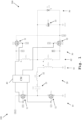
- Fig. 1 illustrates an exemplary embodiment of an LLC converter 100 with synchronous rectification for LED lighting means 50.
- FIG. 1 also depicts an exemplary embodiment of the inventive system 200 comprising the above-mentioned LLC converter 100 and the above-mentioned LED lighting means 50 being supplied by said LLC converter 100.
- the LLC converter 100 comprises a half-bridge 10, a resonant tank 20 comprising a transformer with a primary side 61 and a secondary side 62, a rectification stage 30, and control means 40.
- the half-bridge 10 is configured to supply said primary side 61. Additionally, the secondary side 62 is configured to supply said rectification stage 30.
- the control means 40 are configured to control the operation of switches 11, 12 of the half-bridge 10 and to be supplied with at least one feedback signal indicating the respective switching on-time periods of switches 31, 32 of the rectification stage 30.
- the switches 11, 12 comprise a high-side switch, exemplarily a first field-effect transistor 11, and a low-side switch, exemplarily a second field-effect transistor 12.
- said field-effect transistors 11, 12 are of an n-channel enhancement type.
- switches 31, 32 of the rectification stage 30 comprise a first switch, exemplarily a third field-effect transistor 31, and a second switch, exemplarily a fourth field-effect transistor 32.
- said field-effect transistors 31, 32 are of an n-channel enhancement type.
- switches 31, 32 of the rectification stage 30 are switched in dependence from the respective voltage provided at the secondary side.
- the LLC converter 100 may further comprise an additional control unit, wherein a first terminal, exemplarily a drain terminal, of the third transistor 31, a second terminal, exemplarily a gate terminal, of said third transistor 31, a first terminal, exemplarily a drain terminal, of the fourth transistor 32, and a second terminal, exemplarily a gate terminal, of said fourth transistor 32 are connected to said additional control unit. Additionally or alternatively, the each of the foregoing terminals can be connected to the control means 40.
- the third transistor 31 may especially be turned on if a voltage at the first terminal, exemplarily a drain voltage, of said third transistor 31 falls below a specific turn-on threshold, for instance, -265 mV, and turned off if said voltage at the first terminal, exemplarily said drain voltage, of the third transistor 31 rises above a specific turn-off threshold, for example, 10.5 mV.
- a specific turn-on threshold for instance, -265 mV
- a specific turn-off threshold for example, 10.5 mV.
- control means 40 are configured to detect an asymmetric duty cycle distribution between the switches 31, 32 of the rectification stage 30 on the basis of the at least one feedback signal, exemplarily two feedback signals.
- each of the above-mentioned two feedback signals is a respective gate voltage signal with respect to the field-effect transistors 31, 32 of the rectification stage 30.
- control means 40 are configured to control the operation of the switches 11, 12 of the half-bridge 10 in the sense of an adaption of the respective duty cycles of the switches 11, 12 of the half-bridge.
- a second terminal, exemplarily a gate terminal, of the first transistor 11, and a second terminal, exemplarily a gate terminal, of the second transistor 12 are connected to the control means 40.
- control means 40 may preferably be configured to reduce an asymmetry with respect to the asymmetric duty cycle distribution with the aid of the adaption of the respective duty cycles of the switches of the half-bridge.
- a first terminal, exemplarily a drain terminal, of said first transistor 11 is connected to a voltage potential, exemplarily a supply voltage
- a third terminal, exemplarily a source terminal, of the first transistor 11 is connected to a first terminal, exemplarily a drain terminal, of the second transistor 12.
- a third terminal, exemplarily a source terminal, of said second transistor 12 is connected to another voltage potential, exemplarily ground.
- first terminal exemplarily the drain terminal
- second transistor 12 is connected to a first terminal of capacitance 21
- a second terminal of said capacitance 21 is connected to a first terminal of an inductance 22.
- a second terminal of said inductance 22 is connected to a first terminal of a corresponding inductance of the primary side 61, whereas a second terminal of said corresponding inductance of the primary side 61 is connected to a voltage potential, exemplarily ground.
- the first terminal, exemplarily the drain terminal, of the third transistor 31 is connected to a first terminal of a corresponding inductance of the secondary side 62
- the first terminal, exemplarily the drain terminal, of the fourth transistor 32 is connected to a second terminal of said corresponding inductance of the secondary side 62.
- an intermediate tap, especially a center tap, of the corresponding inductance of the secondary side 62 is connected to a first terminal of a capacitance, exemplarily an electrolytic capacitor 33, and a first terminal of the LED lighting means 50, whereas a second terminal of said capacitance, exemplarily said electrolytic capacitor 33, and a second terminal of the LED lighting means 50 are connected to a third terminal, exemplarily a source terminal, of the third transistors 31, a third terminal, exemplarily a source terminal, of the fourth transistor 32, and a voltage potential, exemplarily ground or another ground.
- FIG. 2 different time diagrams regarding voltage or current, respectively, are depicted with respect to the respective gate terminals of the transistors of the half-bridge, such as the transistors 11, 12, the half-bridge, such as the half-bridge 10, the respective drain and source terminals of the transistors of the rectification stage, such as the transistors 31, 32, and the respective gate terminals of said transistors of said rectification stage in the context of an exemplary 50/50-duty cycle on the left hand of Fig. 2 and an exemplary 40/60-duty cycle on the right hand with regard to the switches of the half-bridge, such as the switches 11, 12 of the half-bridge 10.
- the inventive dynamic duty cycle adaption especially allows for balancing unsymmetrical current shapes.
- the exemplary duty cycle, especially an initial duty cycle, of 50/50 leads to unilateral secondary currents, whereas on the right side of Fig. 2 , the duty cycle is exemplarily adapted to 40/60 which leads to a similar current distribution.
- FIG. 3 shows a further exemplary embodiment 300 of the inventive LLC converter with synchronous rectification.
- Said embodiment 300 exemplarily a primary side thereof, comprises an electromagnetic interference (EMI) filter 70, a rectifier 71, a power factor correction (PFC) unit 72, a low voltage power supply (LVPS) 73, an application-specific integrated circuit (ASIC) 74, an intermediate frequency (IF) unit 75, and a primary side control unit 41, exemplarily a primary side microcontroller.
- EMI electromagnetic interference
- PFC power factor correction
- LVPS low voltage power supply
- ASIC application-specific integrated circuit
- IF intermediate frequency
- the embodiment 300 exemplarily a secondary side thereof, comprises a synchronous rectifier 39, a pulse-width modulation (PWM) unit 76, a low voltage power supply (LVPS) 77, especially a further LVPS, and a secondary side control unit 42, exemplarily a secondary side microcontroller.
- PWM pulse-width modulation
- LVPS low voltage power supply
- secondary side control unit 42 exemplarily a secondary side microcontroller.
- the primary side control unit 41 is coupled to the secondary side control unit 42 via a galvanic decoupling element, exemplarily an opto-coupler 43 or photocoupler, respectively.
- control means 40 of Fig. 1 may comprise such a primary side control unit 41 and such a secondary side control unit 42 being coupled to said primary side control unit 41 preferably via a galvanic decoupling element, such as the photocoupler 43.
- the secondary side control unit 42 can be configured to compare the respective switching on-time periods of the switches of the rectification stage, such as the switches 31, 32 of the rectification stage 30 of Fig. 1 .
- the secondary side control unit 42 is configured to send a trigger signal to the primary side control unit 41 preferably via the galvanic decoupling element 43 if the respective switching on-time periods of the switches of the rectification stage are different with respect to each other.
- the primary side control unit 41 can be configured to calculate at least one duty cycle correction with respect to the respective duty cycles of the switches of the half-bridge, such as the switches 11, 12 of the half-bridge 10 of Fig. 1 .
- the primary side control unit 41 is configured to apply the at least one duty cycle correction to the respective duty cycles of the switches of the half-bridge.
- the primary side is exemplarily coupled to the secondary side via an LLC safety extra-low voltage (SELV) unit 29.
- SELV LLC safety extra-low voltage
- the PFC unit 72 and the ASIC 74 being connected to said PFC unit 72 are connected to the LLC SELV unit 29, whereas the synchronous rectifier 39 being connected to the LVPS 77 and said LVPS 77 are also connected to the LLC SELV unit 29.
- said ASIC 74 is further connected to the LVPS 73 and the primary side control unit 41. Additionally, said primary side control unit 41 is further connected to the IF unit 75, the LVPS 73, and the EMI filter 70. Said EMI filter 70 is further connected to the rectifier 71 being connected to the PFC unit 72.
- said secondary side control unit 42 is further connected to the PWM unit 76 to which LED lighting means, such as the LED lighting means 50 of Fig. 1 , can be connected.
- said PWM unit 76 is further connected to the synchronous rectifier 39 and the LVPS 77.
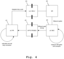
- Fig. 4 depicts a part of the embodiment 300 of Fig. 3 especially to illustrate an exemplary functionality of the inventive duty cycle adaption.
- the secondary side control unit 42 is configured to measure the respective gates, especially gate voltages, of the field-effect transistors of the synchronous rectifier 39, such as the transistors 31, 32 of the rectification stage 30 according to Fig. 1 . Said measurement is preferably performed in a repetitive manner.
- the secondary side control unit 42 is further configured to pass a different gate timing, especially if present, to the primary side control unit 41 through the galvanic decoupling element 43.
- the primary side control unit 41 is configured to calculate and/or set a corresponding duty correction or duty cycle correction, respectively, preferably in a repetitive manner, and to provide an adapted duty cycle for the LLC SELV unit 29 or in the exemplary case of Fig. 1 , for the switches 11, 12 of the half-bridge 10.
Landscapes
- Engineering & Computer Science (AREA)
- Power Engineering (AREA)
- Dc-Dc Converters (AREA)
Abstract
Description
- The invention relates to an LLC converter with synchronous rectification.
- Generally, in times of an increasing use of LED (lightemitting diode) lighting means in many different areas of life, there is a growing need of an LLC converter with synchronous rectification for LED lighting means, and a system comprising such an LLC converter with synchronous rectification and LED lighting means in order to ensure an efficient and reliable supply of said LED lighting means.
- However, there are no LLC converters with synchronous rectification allowing for reducing an asymmetry in the sense of an asymmetric duty cycle distribution between switches of the corresponding rectification stage especially in order to ensure a particularly efficient and reliable supply.
- Accordingly, there is the object to provide an LLC converter with synchronous rectification for LED lighting means, and a system comprising such an LLC converter with synchronous rectification and LED lighting means, thereby ensuring a high efficiency and reliability.
- This object is solved by the features of
claim 1 for an LLC converter with synchronous rectification for LED lighting means and the features of claim 15 for a system comprising such an LLC converter with synchronous rectification and LED lighting means. The dependent claims contain further developments. - According to a first aspect of the invention, an LLC converter with synchronous rectification for LED lighting means is provided. Said LLC converter comprises a half-bridge, a resonant tank comprising a transformer with a primary side and a secondary side, a rectification stage, and control means. In this context, the half-bridge is configured to supply said primary side. Additionally, the secondary side is configured to supply said rectification stage. In further addition to this, the control means are configured to control the operation of switches of the half-bridge and to be supplied with at least one feedback signal indicating the respective switching on-time periods of switches of the rectification stage. Advantageously, this allows for reducing an asymmetry in the sense of an asymmetric duty cycle distribution between the switches of the rectification stage, thereby ensuring a particularly efficient and reliable supply.
- It is noted that the switch, which due to the asymmetry, which carries a much smaller current, can encounter an erroneous switching behavior such small current is difficult to be discriminated from current pulses from noise or the like, such that, for example, an erroneous double switching within one period may occur, which leads to undesired effects even in the light output of connected lighting means. Inventively, as a further advantage, such an erroneous switching behavior is efficiently and reliably prevented. Further advantageously, a correct synchronous rectification can even be guaranteed at low power levels.
- According to a first preferred implementation form of the first aspect of the invention, the switches of the half-bridge comprise a high-side switch, preferably a first transistor, more preferably a first field-effect transistor, and a low-side switch, preferably a second transistor, more preferably a second field-effect transistor. Advantageously, for instance, complexity can be reduced, thereby increasing efficiency.
- According to a second preferred implementation form of the first aspect of the invention, the switches of the rectification stage comprise a first switch, preferably a third transistor, more preferably a third field-effect transistor, and a second switch, preferably a fourth transistor, more preferably a fourth field-effect transistor. Advantageously, for example, simplicity, and thus also cost-efficiency, can be increased.
- According to a further preferred implementation form of the first aspect of the invention, the switches of the rectification stage are switched in dependence from the respective voltage provided at the secondary side. Advantageously, for instance, this allows for a costefficient implementation. In this context, further advantageously, the switches can be implemented as field-effect transistors, wherein the respective gate terminal and the respective drain terminals are connected to a control unit and/or to the control means.
- According to a further preferred implementation form of the first aspect of the invention, the control means comprise a primary side control unit and a secondary side control unit being coupled to said primary side control unit preferably via a galvanic decoupling element. Advantageously, for example, the primary side and the secondary side can galvanically be separated in a full manner.
- According to a further preferred implementation form of the first aspect of the invention, the galvanic decoupling element comprises or is a photocoupler. Advantageously, for instance, galvanic separation can be achieved in a cost-efficient manner.
- According to a further preferred implementation form of the first aspect of the invention, the primary side control unit comprises or is a primary side application-specific integrated circuit. In addition to this or as an alternative, the secondary side control unit comprises or is a secondary side application-specific integrated circuit. Advantageously, for example, efficiency and reliability can further be increased.
- According to a further preferred implementation form of the first aspect of the invention, the control means are configured to detect an asymmetric duty cycle distribution between the switches of the rectification stage on the basis of the at least one feedback signal. Advantageously, for instance, an asymmetry detection can be achieved in a simple and efficient manner. In this context, further advantageously, the switches can be implemented as field-effect transistors, wherein the respective gate voltages are measured especially by the control means.
- According to a further preferred implementation form of the first aspect of the invention, the control means are configured to control the operation of the switches of the half-bridge in the sense of an adaption of the respective duty cycles of the switches of the half-bridge. Advantageously, for example, a dynamic duty cycle adaption especially to balance unsymmetrical current shapes can be achieved in an efficient and reliable manner. In this context, further advantageously, the switches can be implemented as field-effect transistors, wherein the respective gate voltages are controlled especially by the control means.
- According to a further preferred implementation form of the first aspect of the invention, the control means are configured to reduce an asymmetry with respect to the asymmetric duty cycle distribution with the aid of the adaption of the respective duty cycles of the switches of the half-bridge. Advantageously, for instance, unsymmetrical current shapes can easily be balanced.
- According to a further preferred implementation form of the first aspect of the invention, the secondary side control unit is configured to compare the respective switching on-time periods of the switches of the rectification stage. Advantageously, for example, a different gate timing can efficiently be detected especially in the case that the switches are implemented as field-effect transistors comprising respective gate terminals.
- According to a further preferred implementation form of the first aspect of the invention, the secondary side control unit is configured to send a trigger signal to the primary side control unit preferably via the galvanic decoupling element if the respective switching on-time periods of the switches of the rectification stage are different with respect to each other. Advantageously, for instance, the primary side control unit can efficiently and reliably be triggered especially to calculate and/or set a duty correction.
- According to a further preferred implementation form of the first aspect of the invention, the primary side control unit is configured to calculate at least one duty cycle correction with respect to the respective duty cycles of the switches of the half-bridge. Advantageously, for example, such a duty cycle correction efficiently allows for a dynamic duty cycle adaption.
- According to a further preferred implementation form of the first aspect of the invention, the primary side control unit is configured to apply the at least one duty cycle correction to the respective duty cycles of the switches of the half-bridge. Advantageously, for instance, the respective gate voltages can efficiently be set in accordance with the at least one duty cycle correction especially in the case that the switches are implemented as field-effect transistors comprising respective gate terminals.
- According to a second aspect of the invention, a system is provided. Said system comprises an LLC converter according to the first aspect of the invention or any of its preferred implementation forms thereof, respectively, and LED lighting means being supplied by said LLC converter. Advantageously, this allows for reducing an asymmetry in the sense of an asymmetric duty cycle distribution between the switches of the rectification stage, thereby ensuring a particularly efficient and reliable supply. Further advantageously, a correct synchronous rectification can even be guaranteed at low power levels.
- Exemplary embodiments of the invention are now further explained with respect to the drawings by way of example only, and not for limitation. In the drawings:
- Fig. 1
- shows an exemplary embodiment of the first aspect of the invention in combination with the second aspect of the invention;
- Fig. 2
- illustrates inventive dynamic duty cycle adaption with the aid of different time diagrams;
- Fig. 3
- shows a further exemplary embodiment of the first aspect of the invention; and
- Fig. 4
- shows a part of
Fig. 3 in greater detail. - Firstly,
Fig. 1 illustrates an exemplary embodiment of anLLC converter 100 with synchronous rectification for LED lighting means 50. - In addition to this, it is noted that said
Fig. 1 also depicts an exemplary embodiment of theinventive system 200 comprising the above-mentionedLLC converter 100 and the above-mentioned LED lighting means 50 being supplied by saidLLC converter 100. - In accordance with
Fig. 1 , theLLC converter 100 comprises a half-bridge 10, aresonant tank 20 comprising a transformer with aprimary side 61 and asecondary side 62, arectification stage 30, and control means 40. - In this context, the half-
bridge 10 is configured to supply saidprimary side 61. Additionally, thesecondary side 62 is configured to supply saidrectification stage 30. In further addition to this, the control means 40 are configured to control the operation ofswitches bridge 10 and to be supplied with at least one feedback signal indicating the respective switching on-time periods ofswitches rectification stage 30. - With respect to said
switches bridge 10, it is noted that theswitches effect transistor 11, and a low-side switch, exemplarily a second field-effect transistor 12. - In this exemplary case, said field-
effect transistors - With respect of the above-mentioned
switches rectification stage 30, it is noted that said switches 31, 32 comprise a first switch, exemplarily a third field-effect transistor 31, and a second switch, exemplarily a fourth field-effect transistor 32. - In this exemplary case, said field-
effect transistors - With respect to the switches or the
transistors switches rectification stage 30 are switched in dependence from the respective voltage provided at the secondary side. - In this context, the
LLC converter 100 may further comprise an additional control unit, wherein a first terminal, exemplarily a drain terminal, of thethird transistor 31, a second terminal, exemplarily a gate terminal, of saidthird transistor 31, a first terminal, exemplarily a drain terminal, of thefourth transistor 32, and a second terminal, exemplarily a gate terminal, of saidfourth transistor 32 are connected to said additional control unit. Additionally or alternatively, the each of the foregoing terminals can be connected to the control means 40. - In this respect, it is further noted that the
third transistor 31 may especially be turned on if a voltage at the first terminal, exemplarily a drain voltage, of saidthird transistor 31 falls below a specific turn-on threshold, for instance, -265 mV, and turned off if said voltage at the first terminal, exemplarily said drain voltage, of thethird transistor 31 rises above a specific turn-off threshold, for example, 10.5 mV. Such a switching behavior may analogously apply tofourth transistor 32. Said switching regarding thethird transistor 31 or thefourth transistors 32, respectively, can be controlled by the above-mentioned additional control unit and/or the control means 40. - Furthermore, the control means 40 are configured to detect an asymmetric duty cycle distribution between the
switches rectification stage 30 on the basis of the at least one feedback signal, exemplarily two feedback signals. - Accordingly, as it can further be seen from
Fig. 1 , the second terminal, exemplarily the gate terminal, of thethird transistor 31, and the second terminal, exemplarily the gate terminal, of thefourth transistor 32 are connected to the control means 40. In other words, each of the above-mentioned two feedback signals is a respective gate voltage signal with respect to the field-effect transistors rectification stage 30. - Moreover, the control means 40 are configured to control the operation of the
switches bridge 10 in the sense of an adaption of the respective duty cycles of theswitches - Accordingly, a second terminal, exemplarily a gate terminal, of the
first transistor 11, and a second terminal, exemplarily a gate terminal, of thesecond transistor 12 are connected to the control means 40. - In this context, the control means 40 may preferably be configured to reduce an asymmetry with respect to the asymmetric duty cycle distribution with the aid of the adaption of the respective duty cycles of the switches of the half-bridge.
- With respect to the first field-
effect transistor 11, it is noted that a first terminal, exemplarily a drain terminal, of saidfirst transistor 11 is connected to a voltage potential, exemplarily a supply voltage, whereas a third terminal, exemplarily a source terminal, of thefirst transistor 11 is connected to a first terminal, exemplarily a drain terminal, of thesecond transistor 12. Additionally, a third terminal, exemplarily a source terminal, of saidsecond transistor 12 is connected to another voltage potential, exemplarily ground. - Furthermore, the above-mentioned first terminal, exemplarily the drain terminal, of the
second transistor 12 is connected to a first terminal ofcapacitance 21, whereas a second terminal of saidcapacitance 21 is connected to a first terminal of aninductance 22. - In addition to this, a second terminal of said
inductance 22 is connected to a first terminal of a corresponding inductance of theprimary side 61, whereas a second terminal of said corresponding inductance of theprimary side 61 is connected to a voltage potential, exemplarily ground. - Moreover, the first terminal, exemplarily the drain terminal, of the
third transistor 31 is connected to a first terminal of a corresponding inductance of thesecondary side 62, whereas the first terminal, exemplarily the drain terminal, of thefourth transistor 32 is connected to a second terminal of said corresponding inductance of thesecondary side 62. - As it can further be seen from
Fig. 1 , an intermediate tap, especially a center tap, of the corresponding inductance of thesecondary side 62 is connected to a first terminal of a capacitance, exemplarily anelectrolytic capacitor 33, and a first terminal of the LED lighting means 50, whereas a second terminal of said capacitance, exemplarily saidelectrolytic capacitor 33, and a second terminal of the LED lighting means 50 are connected to a third terminal, exemplarily a source terminal, of thethird transistors 31, a third terminal, exemplarily a source terminal, of thefourth transistor 32, and a voltage potential, exemplarily ground or another ground. - Now, in accordance with
Fig. 2 , different time diagrams regarding voltage or current, respectively, are depicted with respect to the respective gate terminals of the transistors of the half-bridge, such as thetransistors bridge 10, the respective drain and source terminals of the transistors of the rectification stage, such as thetransistors Fig. 2 and an exemplary 40/60-duty cycle on the right hand with regard to the switches of the half-bridge, such as theswitches bridge 10. - With the aid of said different time diagrams according to
Fig. 2 , the inventive dynamic duty cycle adaption is illustrated. Said dynamic duty cycle adaption especially allows for balancing unsymmetrical current shapes. In the context ofFig. 2 , it is noted that it can be seen that the exemplary duty cycle, especially an initial duty cycle, of 50/50 leads to unilateral secondary currents, whereas on the right side ofFig. 2 , the duty cycle is exemplarily adapted to 40/60 which leads to a similar current distribution. - Furthermore,
Fig. 3 shows a furtherexemplary embodiment 300 of the inventive LLC converter with synchronous rectification. - Said
embodiment 300, exemplarily a primary side thereof, comprises an electromagnetic interference (EMI)filter 70, arectifier 71, a power factor correction (PFC)unit 72, a low voltage power supply (LVPS) 73, an application-specific integrated circuit (ASIC) 74, an intermediate frequency (IF)unit 75, and a primaryside control unit 41, exemplarily a primary side microcontroller. - In addition to this, the
embodiment 300, exemplarily a secondary side thereof, comprises asynchronous rectifier 39, a pulse-width modulation (PWM)unit 76, a low voltage power supply (LVPS) 77, especially a further LVPS, and a secondaryside control unit 42, exemplarily a secondary side microcontroller. - As it can further be seen from
Fig. 3 , the primaryside control unit 41 is coupled to the secondaryside control unit 42 via a galvanic decoupling element, exemplarily an opto-coupler 43 or photocoupler, respectively. - It is noted that the above-mentioned control means 40 of
Fig. 1 may comprise such a primaryside control unit 41 and such a secondaryside control unit 42 being coupled to said primaryside control unit 41 preferably via a galvanic decoupling element, such as thephotocoupler 43. - Furthermore, the secondary
side control unit 42 can be configured to compare the respective switching on-time periods of the switches of the rectification stage, such as theswitches rectification stage 30 ofFig. 1 . - Moreover, it might be particularly advantageous if the secondary
side control unit 42 is configured to send a trigger signal to the primaryside control unit 41 preferably via thegalvanic decoupling element 43 if the respective switching on-time periods of the switches of the rectification stage are different with respect to each other. - It is further noted that the primary
side control unit 41 can be configured to calculate at least one duty cycle correction with respect to the respective duty cycles of the switches of the half-bridge, such as theswitches bridge 10 ofFig. 1 . - In this context, it might be particularly advantageous if the primary
side control unit 41 is configured to apply the at least one duty cycle correction to the respective duty cycles of the switches of the half-bridge. - As it can further be seen from
Fig. 3 , the primary side is exemplarily coupled to the secondary side via an LLC safety extra-low voltage (SELV)unit 29. - In this context, the
PFC unit 72 and theASIC 74 being connected to saidPFC unit 72 are connected to theLLC SELV unit 29, whereas thesynchronous rectifier 39 being connected to theLVPS 77 and saidLVPS 77 are also connected to theLLC SELV unit 29. - With respect to the
ASIC 74, it is noted that saidASIC 74 is further connected to theLVPS 73 and the primaryside control unit 41. Additionally, said primaryside control unit 41 is further connected to theIF unit 75, theLVPS 73, and theEMI filter 70. SaidEMI filter 70 is further connected to therectifier 71 being connected to thePFC unit 72. - Furthermore, with respect to the secondary
side control unit 42, it is noted that said secondaryside control unit 42 is further connected to thePWM unit 76 to which LED lighting means, such as the LED lighting means 50 ofFig. 1 , can be connected. In addition to this, saidPWM unit 76 is further connected to thesynchronous rectifier 39 and theLVPS 77. - Finally,
Fig. 4 depicts a part of theembodiment 300 ofFig. 3 especially to illustrate an exemplary functionality of the inventive duty cycle adaption. - In accordance with
Fig. 4 , the secondaryside control unit 42 is configured to measure the respective gates, especially gate voltages, of the field-effect transistors of thesynchronous rectifier 39, such as thetransistors rectification stage 30 according toFig. 1 . Said measurement is preferably performed in a repetitive manner. - Moreover, the secondary
side control unit 42 is further configured to pass a different gate timing, especially if present, to the primaryside control unit 41 through thegalvanic decoupling element 43. - Furthermore, the primary
side control unit 41 is configured to calculate and/or set a corresponding duty correction or duty cycle correction, respectively, preferably in a repetitive manner, and to provide an adapted duty cycle for theLLC SELV unit 29 or in the exemplary case ofFig. 1 , for theswitches bridge 10. - While various embodiments of the present invention have been described above, it should be understood that they have been presented by way of example only, and not limitation.
- Numerous changes to the disclosed embodiments can be made in accordance with the disclosure herein without departing from the spirit or scope of the invention. Thus, the breadth and scope of the present invention should not be limited by any of the above described embodiments. Rather, the scope of the invention should be defined in accordance with the following claims and their equivalents.
- Although the invention has been illustrated and described with respect to one or more implementations, equivalent alterations and modifications will occur to others skilled in the art upon the reading and understanding of this specification and the annexed drawings. In addition, while a particular feature of the invention may have been disclosed with respect to only one of several implementations, such feature may be combined with one or more other features of the other implementations as may be desired and advantageous for any given or particular application.
Claims (15)
- An LLC converter (100, 300) with synchronous rectification for LED lighting means (50), the LLC converter (100) comprising:a half-bridge (10),a resonant tank (20) comprising a transformer with a primary side (61) and a secondary side (62),a rectification stage (30) having at least two switches (31, 32) , andcontrol means (40),wherein the half-bridge (10) is configured to supply said primary side (61),wherein the secondary side (62) is configured to supply said rectification stage (30), andwherein the control means (40) are configured to control the operation of switches (11, 12) of the half-bridge (10) and is supplied with at least one feedback signal indicating operation parameters, preferably the respective switching on-time periods of each of said switches (31, 32) of the rectification stage (30).
- The LLC converter (100, 300) according to claim 1, wherein the switches (11, 12) of the half-bridge (10) comprise a high-side switch (11), preferably a first transistor, more preferably a first field-effect transistor, and a low-side switch (12), preferably a second transistor, more preferably a second field-effect transistor.
- The LLC converter (100, 300) according to claim 1 or 2, wherein the switches (31, 32) of the rectification stage (30) comprise a first switch (31), preferably a third transistor, more preferably a third field-effect transistor, and a second switch (32), preferably a fourth transistor, more preferably a fourth field-effect transistor.
- The LLC converter (100, 300) according to any of the claims 1 to 3,
wherein the switches (31, 32) of the rectification stage (30) are switched in dependence from the respective voltage provided at the secondary side (62). - The LLC converter (100, 300) according to any of the claims 1 to 4,
wherein the control means (40) comprise a primary side control unit (41) and a secondary side control unit (42) being coupled to said primary side control unit (41) preferably via a galvanic decoupling element (43). - The LLC converter (100, 300) according to claim 5, wherein the galvanic decoupling element (43) comprises or is a photocoupler.
- The LLC converter (100, 300) according to claim 5 or 6, wherein the primary side control unit (41) comprises or is a primary side application-specific integrated circuit, and/or
wherein the secondary side control unit (42) comprises or is a secondary side application-specific integrated circuit. - The LLC converter (100, 300) according to any of the claims 1 to 7,
wherein the control means (40) are configured to detect an asymmetric duty cycle distribution between the switches (31, 32) of the rectification stage (30) on the basis of the at least one feedback signal. - The LLC converter (100, 300) according to any of the claims 1 to 8,
wherein the control means (40) are configured to control the operation of the switches (11, 12) of the half-bridge (10) in the sense of an adaption of the respective duty cycles of the switches (11, 12) of the half-bridge (10). - The LLC converter (100, 300) according to claim 8 and 9,
wherein the control means (40) are configured to reduce an asymmetry with respect to the asymmetric duty cycle distribution with the aid of the adaption of the respective duty cycles of the switches (11, 12) of the half-bridge (10) . - The LLC converter (100, 300) according to any of the claims 5 to 10,
wherein the secondary side control unit (42) is configured to compare the respective switching on-time periods of the switches (31, 32) of the rectification stage (30). - The LLC converter (100, 300) according to claim 11, wherein the secondary side control unit (42) is configured to send a trigger signal to the primary side control unit (41) preferably via the galvanic decoupling element (43) if the respective switching on-time periods of the switches (31, 32) of the rectification stage (30) are different with respect to each other.
- The LLC converter (100, 300) according to claim 12, wherein the primary side control unit (41) is configured to calculate at least one duty cycle correction with respect to the respective duty cycles of the switches (11, 12) of the half-bridge (10).
- The LLC converter (100, 300) according to claim 13, wherein the primary side control unit (41) is configured to apply the at least one duty cycle correction to the respective duty cycles of the switches (11, 12) of the half-bridge (10).
- A system (200) comprising:an LLC converter (100, 300) according to any of the claims 1 to 14, andLED lighting means (50) being supplied by said LLC converter (100, 300).
Priority Applications (2)
| Application Number | Priority Date | Filing Date | Title |
|---|---|---|---|
| EP22197056.9A EP4344038A1 (en) | 2022-09-22 | 2022-09-22 | Llc converter with synchronous rectification |
| PCT/EP2023/075527 WO2024061777A1 (en) | 2022-09-22 | 2023-09-15 | Llc converter with synchronous rectification |
Applications Claiming Priority (1)
| Application Number | Priority Date | Filing Date | Title |
|---|---|---|---|
| EP22197056.9A EP4344038A1 (en) | 2022-09-22 | 2022-09-22 | Llc converter with synchronous rectification |
Publications (1)
| Publication Number | Publication Date |
|---|---|
| EP4344038A1 true EP4344038A1 (en) | 2024-03-27 |
Family
ID=83438473
Family Applications (1)
| Application Number | Title | Priority Date | Filing Date |
|---|---|---|---|
| EP22197056.9A Pending EP4344038A1 (en) | 2022-09-22 | 2022-09-22 | Llc converter with synchronous rectification |
Country Status (2)
| Country | Link |
|---|---|
| EP (1) | EP4344038A1 (en) |
| WO (1) | WO2024061777A1 (en) |
Citations (3)
| Publication number | Priority date | Publication date | Assignee | Title |
|---|---|---|---|---|
| CN106712529A (en) * | 2017-01-17 | 2017-05-24 | 浙江大学 | High-efficiency and high-power density isolation DC-DC (Direct Current-Direct Current) conversion circuit based on GaN |
| WO2019113784A1 (en) * | 2017-12-12 | 2019-06-20 | Astec International Limited | Resonant converters power supplies and control methods for reducing unbalanced currents in resonant converter power supplies |
| EP3754829A1 (en) * | 2019-06-18 | 2020-12-23 | Tridonic GmbH & Co. KG | Llc circuit |
-
2022
- 2022-09-22 EP EP22197056.9A patent/EP4344038A1/en active Pending
-
2023
- 2023-09-15 WO PCT/EP2023/075527 patent/WO2024061777A1/en not_active Ceased
Patent Citations (3)
| Publication number | Priority date | Publication date | Assignee | Title |
|---|---|---|---|---|
| CN106712529A (en) * | 2017-01-17 | 2017-05-24 | 浙江大学 | High-efficiency and high-power density isolation DC-DC (Direct Current-Direct Current) conversion circuit based on GaN |
| WO2019113784A1 (en) * | 2017-12-12 | 2019-06-20 | Astec International Limited | Resonant converters power supplies and control methods for reducing unbalanced currents in resonant converter power supplies |
| EP3754829A1 (en) * | 2019-06-18 | 2020-12-23 | Tridonic GmbH & Co. KG | Llc circuit |
Non-Patent Citations (1)
| Title |
|---|
| YEON CHEOL-O ET AL: "Digital implementation of optimal SR ON-time control and asymmetric duty control in LLC resonant converter", 2015 9TH INTERNATIONAL CONFERENCE ON POWER ELECTRONICS AND ECCE ASIA (ICPE-ECCE ASIA), KOREAN INSTITUTE OF POWER ELECTRONICS, 1 June 2015 (2015-06-01), pages 2031 - 2037, XP033184399, [retrieved on 20150727], DOI: 10.1109/ICPE.2015.7168057 * |
Also Published As
| Publication number | Publication date |
|---|---|
| WO2024061777A1 (en) | 2024-03-28 |
Similar Documents
| Publication | Publication Date | Title |
|---|---|---|
| US9685876B2 (en) | Resonant converter with capacitive mode detection and associated detection method | |
| US11159090B2 (en) | Synchronous rectification of LLC converters based on homopolarity | |
| KR101086737B1 (en) | Current Balancer and Power Supply | |
| US20110188269A1 (en) | Switching power-supply apparatus | |
| US9257901B2 (en) | DC power supply circuit | |
| WO2010117410A1 (en) | Buck converter with iii-nitride switch for substantially increased input-to-output voltage ratio | |
| TW201717530A (en) | Automatic enhanced self-driven synchronous rectification for power converters | |
| JP2009284667A (en) | Power supply device, its control method, and semiconductor device | |
| KR101985385B1 (en) | Switching power supply device and light illuminating apparatus having the same | |
| US9716427B2 (en) | Power factor correction circuit having bottom skip controller | |
| US8541957B2 (en) | Power converter having a feedback circuit for constant loads | |
| US20060013020A1 (en) | Dc converter | |
| CN110100501A (en) | circuit arrangement for operating loads | |
| US11411383B2 (en) | Leakage protection circuit, leakage protection method and load driving circuit | |
| WO2024061777A1 (en) | Llc converter with synchronous rectification | |
| KR20070110997A (en) | Switch drive device, half bridge converter using the same and driving method thereof | |
| US20140184102A1 (en) | Light emitting diode driving device | |
| US9426854B1 (en) | Electronic driver for controlling an illumination device | |
| KR20160011497A (en) | High-efficiency single-stage ac/dc converter for power factor correction | |
| US11342857B2 (en) | Synchronous rectification controller and isolated synchronous rectification type dc/dc converter | |
| US11705814B2 (en) | Switching control circuit and LLC converter | |
| CN102577064B (en) | Operating device for luminous elements | |
| EP4462665B1 (en) | Isolated, primary side switched resonant conversion for supplying a led load | |
| JP2012244757A (en) | Switching power supply | |
| US11448669B2 (en) | Current sensor and measuring method for the switched sensing of an alternating current |
Legal Events
| Date | Code | Title | Description |
|---|---|---|---|
| PUAI | Public reference made under article 153(3) epc to a published international application that has entered the european phase |
Free format text: ORIGINAL CODE: 0009012 |
|
| STAA | Information on the status of an ep patent application or granted ep patent |
Free format text: STATUS: THE APPLICATION HAS BEEN PUBLISHED |
|
| AK | Designated contracting states |
Kind code of ref document: A1 Designated state(s): AL AT BE BG CH CY CZ DE DK EE ES FI FR GB GR HR HU IE IS IT LI LT LU LV MC MK MT NL NO PL PT RO RS SE SI SK SM TR |
|
| STAA | Information on the status of an ep patent application or granted ep patent |
Free format text: STATUS: REQUEST FOR EXAMINATION WAS MADE |
|
| 17P | Request for examination filed |
Effective date: 20240701 |
|
| RBV | Designated contracting states (corrected) |
Designated state(s): AL AT BE BG CH CY CZ DE DK EE ES FI FR GB GR HR HU IE IS IT LI LT LU LV MC MK MT NL NO PL PT RO RS SE SI SK SM TR |
|
| GRAP | Despatch of communication of intention to grant a patent |
Free format text: ORIGINAL CODE: EPIDOSNIGR1 |
|
| STAA | Information on the status of an ep patent application or granted ep patent |
Free format text: STATUS: GRANT OF PATENT IS INTENDED |